EP4404718A1 - Organische leuchtdiode und organische lichtemittierende vorrichtung - Google Patents
Organische leuchtdiode und organische lichtemittierende vorrichtung Download PDFInfo
- Publication number
- EP4404718A1 EP4404718A1 EP23195036.1A EP23195036A EP4404718A1 EP 4404718 A1 EP4404718 A1 EP 4404718A1 EP 23195036 A EP23195036 A EP 23195036A EP 4404718 A1 EP4404718 A1 EP 4404718A1
- Authority
- EP
- European Patent Office
- Prior art keywords
- unsubstituted
- substituted
- host
- layer
- electrode
- Prior art date
- Legal status (The legal status is an assumption and is not a legal conclusion. Google has not performed a legal analysis and makes no representation as to the accuracy of the status listed.)
- Granted
Links
Images


Classifications
-
- H—ELECTRICITY
- H10—SEMICONDUCTOR DEVICES; ELECTRIC SOLID-STATE DEVICES NOT OTHERWISE PROVIDED FOR
- H10K—ORGANIC ELECTRIC SOLID-STATE DEVICES
- H10K50/00—Organic light-emitting devices
- H10K50/10—OLEDs or polymer light-emitting diodes [PLED]
- H10K50/11—OLEDs or polymer light-emitting diodes [PLED] characterised by the electroluminescent [EL] layers
- H10K50/12—OLEDs or polymer light-emitting diodes [PLED] characterised by the electroluminescent [EL] layers comprising dopants
-
- H—ELECTRICITY
- H10—SEMICONDUCTOR DEVICES; ELECTRIC SOLID-STATE DEVICES NOT OTHERWISE PROVIDED FOR
- H10K—ORGANIC ELECTRIC SOLID-STATE DEVICES
- H10K50/00—Organic light-emitting devices
- H10K50/10—OLEDs or polymer light-emitting diodes [PLED]
- H10K50/11—OLEDs or polymer light-emitting diodes [PLED] characterised by the electroluminescent [EL] layers
- H10K50/125—OLEDs or polymer light-emitting diodes [PLED] characterised by the electroluminescent [EL] layers specially adapted for multicolour light emission, e.g. for emitting white light
- H10K50/13—OLEDs or polymer light-emitting diodes [PLED] characterised by the electroluminescent [EL] layers specially adapted for multicolour light emission, e.g. for emitting white light comprising stacked EL layers within one EL unit
- H10K50/131—OLEDs or polymer light-emitting diodes [PLED] characterised by the electroluminescent [EL] layers specially adapted for multicolour light emission, e.g. for emitting white light comprising stacked EL layers within one EL unit with spacer layers between the electroluminescent layers
-
- C—CHEMISTRY; METALLURGY
- C09—DYES; PAINTS; POLISHES; NATURAL RESINS; ADHESIVES; COMPOSITIONS NOT OTHERWISE PROVIDED FOR; APPLICATIONS OF MATERIALS NOT OTHERWISE PROVIDED FOR
- C09K—MATERIALS FOR MISCELLANEOUS APPLICATIONS, NOT PROVIDED FOR ELSEWHERE
- C09K11/00—Luminescent materials, e.g. electroluminescent or chemiluminescent
- C09K11/06—Luminescent materials, e.g. electroluminescent or chemiluminescent containing organic luminescent materials
-
- H—ELECTRICITY
- H10—SEMICONDUCTOR DEVICES; ELECTRIC SOLID-STATE DEVICES NOT OTHERWISE PROVIDED FOR
- H10K—ORGANIC ELECTRIC SOLID-STATE DEVICES
- H10K50/00—Organic light-emitting devices
- H10K50/10—OLEDs or polymer light-emitting diodes [PLED]
- H10K50/11—OLEDs or polymer light-emitting diodes [PLED] characterised by the electroluminescent [EL] layers
-
- H—ELECTRICITY
- H10—SEMICONDUCTOR DEVICES; ELECTRIC SOLID-STATE DEVICES NOT OTHERWISE PROVIDED FOR
- H10K—ORGANIC ELECTRIC SOLID-STATE DEVICES
- H10K50/00—Organic light-emitting devices
- H10K50/10—OLEDs or polymer light-emitting diodes [PLED]
- H10K50/11—OLEDs or polymer light-emitting diodes [PLED] characterised by the electroluminescent [EL] layers
- H10K50/125—OLEDs or polymer light-emitting diodes [PLED] characterised by the electroluminescent [EL] layers specially adapted for multicolour light emission, e.g. for emitting white light
- H10K50/13—OLEDs or polymer light-emitting diodes [PLED] characterised by the electroluminescent [EL] layers specially adapted for multicolour light emission, e.g. for emitting white light comprising stacked EL layers within one EL unit
-
- H—ELECTRICITY
- H10—SEMICONDUCTOR DEVICES; ELECTRIC SOLID-STATE DEVICES NOT OTHERWISE PROVIDED FOR
- H10K—ORGANIC ELECTRIC SOLID-STATE DEVICES
- H10K50/00—Organic light-emitting devices
- H10K50/10—OLEDs or polymer light-emitting diodes [PLED]
- H10K50/14—Carrier transporting layers
- H10K50/15—Hole transporting layers
-
- H—ELECTRICITY
- H10—SEMICONDUCTOR DEVICES; ELECTRIC SOLID-STATE DEVICES NOT OTHERWISE PROVIDED FOR
- H10K—ORGANIC ELECTRIC SOLID-STATE DEVICES
- H10K50/00—Organic light-emitting devices
- H10K50/10—OLEDs or polymer light-emitting diodes [PLED]
- H10K50/18—Carrier blocking layers
- H10K50/181—Electron blocking layers
-
- H—ELECTRICITY
- H10—SEMICONDUCTOR DEVICES; ELECTRIC SOLID-STATE DEVICES NOT OTHERWISE PROVIDED FOR
- H10K—ORGANIC ELECTRIC SOLID-STATE DEVICES
- H10K59/00—Integrated devices, or assemblies of multiple devices, comprising at least one organic light-emitting element covered by group H10K50/00
- H10K59/10—OLED displays
-
- H—ELECTRICITY
- H10—SEMICONDUCTOR DEVICES; ELECTRIC SOLID-STATE DEVICES NOT OTHERWISE PROVIDED FOR
- H10K—ORGANIC ELECTRIC SOLID-STATE DEVICES
- H10K59/00—Integrated devices, or assemblies of multiple devices, comprising at least one organic light-emitting element covered by group H10K50/00
- H10K59/10—OLED displays
- H10K59/12—Active-matrix OLED [AMOLED] displays
-
- H—ELECTRICITY
- H10—SEMICONDUCTOR DEVICES; ELECTRIC SOLID-STATE DEVICES NOT OTHERWISE PROVIDED FOR
- H10K—ORGANIC ELECTRIC SOLID-STATE DEVICES
- H10K85/00—Organic materials used in the body or electrodes of devices covered by this subclass
- H10K85/60—Organic compounds having low molecular weight
- H10K85/615—Polycyclic condensed aromatic hydrocarbons, e.g. anthracene
-
- H—ELECTRICITY
- H10—SEMICONDUCTOR DEVICES; ELECTRIC SOLID-STATE DEVICES NOT OTHERWISE PROVIDED FOR
- H10K—ORGANIC ELECTRIC SOLID-STATE DEVICES
- H10K85/00—Organic materials used in the body or electrodes of devices covered by this subclass
- H10K85/60—Organic compounds having low molecular weight
- H10K85/615—Polycyclic condensed aromatic hydrocarbons, e.g. anthracene
- H10K85/626—Polycyclic condensed aromatic hydrocarbons, e.g. anthracene containing more than one polycyclic condensed aromatic rings, e.g. bis-anthracene
-
- H—ELECTRICITY
- H10—SEMICONDUCTOR DEVICES; ELECTRIC SOLID-STATE DEVICES NOT OTHERWISE PROVIDED FOR
- H10K—ORGANIC ELECTRIC SOLID-STATE DEVICES
- H10K85/00—Organic materials used in the body or electrodes of devices covered by this subclass
- H10K85/60—Organic compounds having low molecular weight
- H10K85/649—Aromatic compounds comprising a hetero atom
- H10K85/657—Polycyclic condensed heteroaromatic hydrocarbons
- H10K85/6574—Polycyclic condensed heteroaromatic hydrocarbons comprising only oxygen in the heteroaromatic polycondensed ring system, e.g. cumarine dyes
-
- H—ELECTRICITY
- H10—SEMICONDUCTOR DEVICES; ELECTRIC SOLID-STATE DEVICES NOT OTHERWISE PROVIDED FOR
- H10K—ORGANIC ELECTRIC SOLID-STATE DEVICES
- H10K2101/00—Properties of the organic materials covered by group H10K85/00
- H10K2101/30—Highest occupied molecular orbital [HOMO], lowest unoccupied molecular orbital [LUMO] or Fermi energy values
-
- H—ELECTRICITY
- H10—SEMICONDUCTOR DEVICES; ELECTRIC SOLID-STATE DEVICES NOT OTHERWISE PROVIDED FOR
- H10K—ORGANIC ELECTRIC SOLID-STATE DEVICES
- H10K2101/00—Properties of the organic materials covered by group H10K85/00
- H10K2101/40—Interrelation of parameters between multiple constituent active layers or sublayers, e.g. HOMO values in adjacent layers
-
- H—ELECTRICITY
- H10—SEMICONDUCTOR DEVICES; ELECTRIC SOLID-STATE DEVICES NOT OTHERWISE PROVIDED FOR
- H10K—ORGANIC ELECTRIC SOLID-STATE DEVICES
- H10K2101/00—Properties of the organic materials covered by group H10K85/00
- H10K2101/90—Multiple hosts in the emissive layer
-
- H—ELECTRICITY
- H10—SEMICONDUCTOR DEVICES; ELECTRIC SOLID-STATE DEVICES NOT OTHERWISE PROVIDED FOR
- H10K—ORGANIC ELECTRIC SOLID-STATE DEVICES
- H10K50/00—Organic light-emitting devices
- H10K50/10—OLEDs or polymer light-emitting diodes [PLED]
- H10K50/19—Tandem OLEDs
Definitions
- the present invention relates to an organic light emitting diode, and more particularly to, an organic light emitting diode (OLED) that has low power consumption, improved luminous efficiency and/or luminous lifespan, as well as to an organic light emitting device including the OLED (e.g. , a display device or a lighting device).
- OLED organic light emitting diode
- OLED organic light emitting diode
- LCD liquid crystal display device
- the OLED can be formed as a thin organic film less than 2000 ⁇ and the electrode configurations can implement unidirectional or bidirectional images.
- the OLED can be formed even on a flexible transparent substrate such as a plastic substrate so that a flexible or a foldable display device can be realized with ease using the OLED.
- the OLED can be driven at a lower voltage and the OLED has advantageous high color purity compared to the LCD.
- embodiments of the present invention are directed to an organic light emitting diode and an organic light emitting device that substantially obviate one or more of the problems due to the limitations and disadvantages of the related art.
- An aspect of the present invention is to provide an organic light emitting diode that can implement low power consumption and has beneficial luminous efficiency and luminous lifespan, as well as an organic light emitting device including the diode.
- the present invention provides an organic light emitting diode that includes a first electrode; a second electrode facing the first electrode; and an emissive layer disposed between the first and second electrode, and including at least one blue emitting material layer, wherein the at least one blue emitting material layer includes a first host having the following structure of Chemical Formula 1 and a second host having the following structure of Chemical Formula 3: wherein, in the Chemical Formula 1,
- R 1 is an unsubstituted or substituted naphthalene, or phenanthrene group
- R 2 is an unsubstituted or substituted naphthalene group
- each of R 3 and R 4 is independently hydrogen, deuterium, methyl, ethyl or propyl
- each of L 1 and L 2 is independently a single bond or an unsubstituted or substituted phenyl group
- R 11 is an unsubstituted or substituted naphthalene, or phenanthrene group
- R 12 is independently an unsubstituted or substituted dibenzofuran, or carbazole group
- each of R 13 and R 14 is independently hydrogen, deuterium, methyl, ethyl or propyl
- each of L 11 and L 12 is independently a single bond or an unsubstituted or substituted phenyl group.
- each of R 1 and R 2 is independently an unsubstituted or substituted dibenzofuran, carbazole, naphthalene, or phenanthrene group; each of R 3 and R 4 is independently hydrogen, deuterium, methyl, ethyl or propyl; and each of L 1 and L 2 is independently a single bond or an unsubstituted or substituted phenyl group, and wherein in the Chemical Formula 3, each of R 11 and R 12 is independently an unsubstituted or substituted dibenzofuran, carbazole, naphthalene, or phenanthrene group; each of R 13 and R 14 is independently hydrogen, deuterium, methyl, ethyl or propyl; and each of L 11 and L 12 is independently a single bond, an unsubstituted or substituted C 6 -C 30 arylene group or an unsubstituted or a phenyl group.
- the first host is at least one of the following organic compounds:
- the first host and the second host in the at least one blue emitting material layers can be admixed with a weight ratio of about 9:1 to about 7:3. In other aspects, the first host and the second host in the at least one blue emitting material layers can be admixed with a weight ratio of about 8:2 or about 6:4.
- the first host can have a highest occupied molecular orbital (HOMO) energy level lower than a HOMO energy level of the second host.
- HOMO highest occupied molecular orbital
- the first host has a HOMO energy level between about -5.9 eV and about -6.1 eV and/or the second host has a HOMO energy level between about -5.8 eV and about -5.9 eV.
- the emissive layer can further include at least one hole transport layer or at least one electron blocking layer disposed between the first electrode and the at least one blue emitting material layer, wherein an energy bandgap between a HOMO energy level of hole transporting material in the at least one hole transport layer or electron blocking material in the at least one electron blocking layer, and a HOMO energy level of at least one of the first host and the second host in the at least one blue emitting material layer can be about 0.15 eV or less.
- the emissive layer can further include a first emitting part disposed between the first electrode and the second electrode, and including a first blue emitting material layer; a second emitting part disposed between the first emitting part and the second electrode; a third emitting part disposed between the second emitting part and the second electrode, and including a second blue emitting material layer; a first charge generation layer disposed between the first emitting part and the second emitting part; and a second charge generation layer disposed between the second emitting part and the third emitting part, wherein at least one of the first blue emitting material layer and the second blue emitting material layer can include the first host and the second host.
- the present invention provides an organic light emitting diode that includes a first electrode; a second electrode facing the first electrode; and an emissive layer disposed between the first electrode and the second electrode, wherein the emissive layer includes: a first emitting part disposed between the first electrode and the second electrode, and including a first blue emitting material layer; a second emitting part disposed between the first emitting part and the second electrode; a third emitting part disposed between the second emitting part and the second electrode, and including a second blue emitting material layer; a first charge generation layer disposed between the first emitting part and the second emitting part; and a second charge generation layer disposed between the second emitting part and the third emitting part, and wherein the second blue emitting material layer includes a first host having the structure of Chemical Formula 1 and a second host having the structure of Chemical Formula 3.
- each organic light emitting diode (OLED) and each organic light emitting device (e.g., display device, illumination device, etc.) using the OLED are operatively coupled and configured.
- the organic light emitting display device 100 includes a substrate 102, a thin-film transistor Tr on the substrate 102, and an organic light emitting diode D connected to the thin film transistor Tr.
- the substrate 102 can include a red pixel region, a green pixel region and a blue pixel region and an organic light emitting diode D can be located in each pixel region.
- Each of the organic light emitting diodes D emitting red, green and blue light, respectively, is located correspondingly in the red pixel region, the green pixel region and the blue pixel region.
- the organic light emitting diode D can be disposed in the blue pixel region.
- a semiconductor layer 110 is disposed on the buffer layer 106.
- the semiconductor layer 110 can include, but is not limited to, oxide semiconductor materials.
- a light-shield pattern can be disposed under the semiconductor layer 110, and the light-shield pattern can prevent light from being incident toward the semiconductor layer 110, thereby, preventing or reducing the semiconductor layer 110 from being degraded by the light.
- the semiconductor layer 110 can include polycrystalline silicon. In this case, opposite edges of the semiconductor layer 110 can be doped with impurities.
- a source electrode 152 and a drain electrode 154 which are made of conductive material such as a metal, are disposed on the interlayer insulating layer 140.
- the source electrode 152 and the drain electrode 154 are spaced apart from each other on opposing sides of the gate electrode 130, and contact both sides of the semiconductor layer 110 through the first and second semiconductor layer contact holes 142 and 144, respectively.
- a passivation layer 160 is disposed on the source and drain electrodes 152 and 154.
- the passivation layer 160 covers the thin film transistor Tr on the entire substrate 102.
- the passivation layer 160 has a flat top surface and a drain contact hole (or a contact hole) 162 that exposes or does not cover the drain electrode 154 of the thin film transistor Tr. While the drain contact hole 162 is disposed on the second semiconductor layer contact hole 144, it can be spaced apart from the second semiconductor layer contact hole 144.
- the second electrode 220 is disposed on the substrate 102 above which the emissive layer 230 is disposed.
- the second electrode 220 can be disposed on the entire display area.
- the second electrode 220 can include a conductive material with a relatively low work function value compared to the first electrode 210.
- the second electrode 220 can be a cathode providing electrons.
- an encapsulation film 170 can be disposed on the second electrode 220 in order to prevent or reduce outer moisture from penetrating into the OLED D.
- the encapsulation film 170 can have, but is not limited to, a laminated structure of a first inorganic insulating film 172, an organic insulating film 174 and a second inorganic insulating film 176. In certain embodiments, the encapsulation film 170 can be omitted.
- a polarizing plate can be attached onto the encapsulation film 170 to reduce reflection of external light.
- the polarizing plate can be a circular polarizing plate.
- the polarizing plate can be disposed under the substrate 102.
- the polarizing plate can be disposed on the encapsulation film 170.
- a cover window can be attached to the encapsulation film 170 or the polarizing plate.
- the substrate 102 and the cover window can have a flexible property, thus the organic light emitting display device 100 can be a flexible display device.
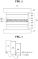
- FIG. 3 illustrates a schematic cross-sectional view of an organic light emitting diode having a single emitting part in accordance with an embodiment of the present invention.
- FIG. 3 shows an example (OLED D1) of the OLED D in FIGS. 1 and 2 .
- the first electrode 210 can be an anode that provides a hole into the EML 340.
- the first electrode 210 can include a conductive material having a relatively high work function value, for example, a transparent conductive oxide (TCO).
- TCO transparent conductive oxide
- the first electrode 210 can include, but is not limited to, indium tin oxide (ITO), indium zinc oxide (IZO), indium tin zinc oxide (ITZO), tin oxide (SnO), zinc oxide (ZnO), indium cerium oxide (ICO), aluminum doped zinc oxide (AZO), and/or combinations thereof.
- the second electrode 220 can be a cathode that provides an electron into the EML 340.
- the second electrode 220 can include a conductive material having a relatively low work function value.
- the second electrode 220 can include highly reflective material such as aluminum (Al), magnesium (Mg), calcium (Ca), silver (Ag), alloy thereof and/or combinations thereof such as aluminum-magnesium alloy (Al-Mg).
- Al-Mg aluminum-magnesium alloy
- the EML 340 includes a host including a first host 342 and a second host 344 and a blue emitter (blue dopant) 346 where the substantial light emission is occurred.
- Haldrogen as used herein, can refer to protium, deuterium and tritium.
- substituted means that the hydrogen is replaced with a substituent.
- the substituent can comprise, but is not limited to, an unsubstituted or halogen-substituted C 1 -C 20 alkyl group, an unsubstituted or halogen-substituted C 1 -C 20 alkoxy, halogen, a cyano group, a hydroxyl group, a carboxylic group, a carbonyl group, an amino group, a C 1 -C 10 alkyl amino group, a C 6 -C 30 aryl amino group, a C 3 -C 30 hetero aryl amino group, a nitro group, a hydrazyl group, a sulfonate group, a C 1 -C 10 alkyl silyl group, a C 1 -C 10 alkoxy silyl group, a C 3 -C 20 cyclo alkyl silyl group, a C 6 -C 30
- the aryl group can independently include, but is not limited to, an unfused or fused aryl group such as phenyl, biphenyl, terphenyl, naphthyl, anthracenyl, pentalenyl, indenyl, indeno-indenyl, heptalenyl, biphenylenyl, indacenyl, phenalenyl, phenanthrenyl, benzo-phenanthrenyl, dibenzo-phenanthrenyl, azulenyl, pyrenyl, fluoranthenyl, triphenylenyl, chrysenyl, tetraphenylenyl, tetracenyl, pleiadenyl, picenyl, pentaphenylenyl, pentacenyl, fluorenyl, indeno-fluorenyl or spiro-fluorenyl.
- aryl group such as
- each of the aryl group or the hetero aryl group can consist of one to four aromatic and/or hetero aromatic rings.
- the number of the aromatic and/or hetero aromatic rings of R 1 to R 4 becomes more than four, conjugated structure within the whole molecule becomes too long, thus, the organometallic compound can have too narrow energy bandgap.
- each of R 1 and R 2 in Chemical Formula 1 can be independently a C 6 -C 20 aryl group such as naphthyl (e.g., 1-napthyl or 2-naphthyl) and phenanthrenyl
- each of R 3 and R 4 can be independently hydrogen or a C 1 -C 10 alkyl group ( e.g ., methyl or tert-butyl)
- each of L 1 and L 2 can be independently a single bond or a C 6 -C 20 arylene group (e.g ., phenylene), but is not limited thereto.
- the first host 342 having the structure of Chemical Formula 1 can include, but is not limited to, 9,10-di(naphthalen-2-yl)anthracene (ADN), 2-methyl-9,10-bis(naphthalen-2-yl)anthracene (MADN), 2-tert-Butyl-9,10-di(naphthen-2-yl)anthracene (TBADN), 9,10-di(naphthalen-2-yl)-2-phenylanthracene (PADN), 9,10-di(1-naphthyl)anthracene, 9-(naphthalene-1-yl)-10-(naphthalene-2-yl)anthracene, 9-(2-napthyl)-10-[4-(1-naphthyl)phenyl]anthracene, 9-(1-napthyl)-10-[4-(2-naphthyl)phenyl
- the first host 342 can be, but is not limited to, at least one of the organic compounds BH1-1 to BH1-8 as disclosed above.
- the first host 342 can have HOMO energy level between about -5.9 eV and about -6.1 eV, for example, less than about -5.9 eV and about -6.1 eV, and can have an excited triplet energy level between about 1.7 eV and 1.9 eV, but is not limited thereto.
- the second host 344 can be an organic compound where at least one hetero aryl group is linked to an anthracene core directly or via a linking group.
- the second host 344 can be an anthracene-based organic compound having the following structure of Chemical Formula 3: wherein, in the Chemical Formula 3,
- Each of the C 6 -C 30 aryl group and/or the C 3 -C 30 hetero aryl group of R 11 to R 14 in Chemical Formula 3 can be independently unsubstituted or substituted with at least one group selected from a C 1 -C 10 alkyl group, a C 6 -C 20 aryl group and a C 3 -C 20 hetero aryl group.
- the holes accumulated in the interface between the blue emitting material layer EML, and the HTL 320 and/or the EBL 330 cannot be recombined with electrons and quenched as non-emission.
- the luminous efficiency of an organic light emitting diode can be lowered as sufficient excitons are not generated in the conventional blue emitting material layer EML.
- the driving voltage of the organic light emitting diode can be raised as holes not injected into the conventional blue emitting material layer EML are quenched as non-emission.
- FIG. 5 illustrates a schematic diagram showing energy levels among a common layer and a blue emitting material layer in an organic light emitting diode with a single emitting unit in accordance with an embodiment of the present invention.
- the blue emitting material layer 340 (EML) in the OLED D1 can include the first host 342 and the second host 344.
- the first host 342 has a HOMO energy level between about -5.9 eV and about -6.1 eV and the second host 344 has a HOMO energy level between about -5.8 eV and about -5.9 eV.
- the energy bandgap ⁇ HOMO2 between the HOMO energy level of the host in the blue EML 340 including the first and second hosts 342 and 344, and the HOMO energy level of the hole transporting material in the HTL and/or the electron blocking material in the EBL 330 can be reduced significantly compared to the energy bandgap ⁇ HOMO1 between the HOMO energy level of the host in the conventional blue emitting material layer using the single host, and the HOMO energy level of the hole transporting material and/or the electron blocking material.
- the energy bandgap ⁇ HOMO2 between the HOMO energy level of the host in the blue EML 340 including both the first and second hosts 342 and 344, and the HOMO energy level of the hole transporting material and/or the electron blocking material can be about 0.15 eV or less, for example, about 0.1 eV or less.
- the holes generated at the first electrode 210 can be injected rapidly into the blue EML 340 via the HTL 320 and the EBL 330. Since the holes injected efficiently into the blue EML 340 can be recombined with electrons to generate effective excitons, the luminous efficiency of the OLED D1 can be improved.
- the HIL 310 is disposed between the first electrode 210 and the HTL 320 and can improve an interface property between the inorganic first electrode 210 and the organic HTL 320.
- the HIL 310 can include, but is not limited to, 4,4',4"-Tris(3-methylphenylamino)triphenylamine (MTDATA), 4,4',4"-Tris(N,N-diphenyl-amino)triphenylamine (NATA), 4,4',4"-Tris(N-(naphthalene-1-yl)-N-phenyl-amino)triphenylamine (1T-NATA), 4,4',4"-Tris(N-(naphthalene-2-yl)-N-phenyl-amino)triphenylamine (2T-NATA), Copper phthalocyanine (CuPc), Tris(4-carbazoyl-9-yl-phenyl)amine (TCTA), N,N'-
- the HIL 310 can include the hole transporting material described below doped with the above hole injecting material (e.g ., organic material such as HAT-CN, F4-TCNA and/or F6-TCNNQ and/or inorganic material such as MgF 2 and/or CaF 2 ).
- the contents of the hole injecting material in the HIL 310 can be, but is not limited to, about 1 wt% to about 50 wt%, for example, about 5 wt% to about 50 wt%.
- the HIL 310 can be omitted in compliance of the OLED D1 property.
- the ETL 360 and the EII, 370 can be laminated sequentially between the EML 340 and the second electrode 220.
- An electron transporting material included in the ETL 360 has high electron moibity so as to provide electrons stably with the EML 340 by fast electron transportation.
- the ETL 360 can include, but is not limited to, tris-(8-hydroxyquinoline) aluminum (Alq 3 ), 2-biphenyl-4-yl-5-(4-t-butylphenyl)-1,3,4-oxadiazole (PBD), spiro-PBD, lithium quinolate (Liq), 2,2', 2"-(1,3,5-benzenetriyl)-tris(1-phenyl-1-H-benzimidazole) (TPBi), Bis(2-methyl-8-quinolinolato-N1,O8)-(1,1'-biphenyl-4-olato)aluminum (BAlq), 4,7-diphenyl-1,10-phenanthroline (Bphen), 2,9-Bis(naphthalene-2-yl)4,7-diphenyl-1,10-phenanthroline (NBphen), 2,9-Dimethyl-4,7-diphenyl-1,10-phenathroline (BCP),
- the EII, 370 is disposed between the second electrode 220 and the ETL 360, and can improve physical properties of the second electrode 220 and therefore, can enhance the lifespan of the OLED D1.
- the EIL 370 can include, but is not limited to, an alkali metal halide and/or an alkaline earth metal halide such as LiF, CsF, NaF, BaF 2 and the like, and/or an organometallic compound such as Liq, lithium benzoate, sodium stearate, and the like.
- the ETL 360 and the EIL 370 can have a single layered structure.
- the above electron transporting material and/or the electron injecting material can be admixed with each other.
- the ETL/EIL can include two or more different electron transporting materials.
- two electron transporting materials in the ETL/EIL are admixed with, but is not limited to, a weight ratio of about 3:7 to about 7:3.
- the EBL 330 can include, but is not limited to, TCTA, N-(biphenyl-4-yl)-9,9-dimethyl-N-(4-(9-phenyl-9H-carbazol-3-yl)phenyl)-9H-fluoren-2-amine, TAPC, MTDATA, 1,3-Bis(carbazol-9-yl)benzene (mCP), 3,3-Di(9H-carbazol-9-yl)biphenyl (mCBP), CuPc, DNTPD, TDABP, DCDPA, 2,8-bis(9-phenyl-9H-carbazol-3-yl)dibenzo[b,d]thiophene and/or combinations thereof.
- TCTA N-(biphenyl-4-yl)-9,9-dimethyl-N-(4-(9-phenyl-9H-carbazol-3-yl)phenyl)-9H-fluoren-2-amine
- TAPC
- the OLED D1 in accordance with this aspect of the present invention can further include the HBL 350 between the EML 340 and the ETL 360 so that holes cannot be transferred from the EML 340 to the ETL 360.
- the HBL 350 can include, but is not limited to, at least one of an oxadiazole-based compound, a triazole-based compound, a phenanthroline-based compound, a benzoxazole-based compound, a benzothiazole-based compound, a benzimidazole-based compound, and a triazine-based compound.
- the HBL 350 can include material having a relatively low HOMO energy level compared to the luminescent materials in EML 340.
- the HBL 350 can include, but is not limited to, BCP, BAlq, Alq 3 , PBD, spiro-PBD, Liq, Bis-4,5-(3,5-di-3-pyridylphenyl)-2-methylpyrimidine (B3PYMPM), DPEPO, 9-(6-(9H-carbazol-9-yl)pyridine-3-yl)-9H-3,9'-bicarbazole, TSPO1 and/or combinations thereof.
- each of the EBL 330 and/or the HBL 350 can be omitted.
- FIG. 6 illustrates a schematic cross-sectional view of an organic light emitting display device in accordance with another embodiment of the present invention.
- an organic light emitting display device 400 comprises a first substrate 402 that defines each of a red pixel region RP, a green pixel region GP and a blue pixel region BP, a second substrate 404 facing the first substrate 402, a thin film transistor Tr on the first substrate 402, an organic light emitting diode (OLED) D disposed between the first and second substrates 402 and 404 and emitting white (W) light and a color filter layer 480 disposed between the OLED D and the first substrate 402.
- the organic light emitting display device 400 can include a plurality of such pixel regions arranged in a matrix configuration or other suitable configurations.
- Each of the first and second substrates 402 and 404 can include, but is not limited to, glass, flexible material and/or polymer plastics.
- each of the first and second substrates 402 and 404 can be made of PI, PES, PEN, PET, PC and/or combinations thereof.
- a buffer layer 406 can be disposed on the first substrate 402.
- the thin film transistor Tr is disposed on the buffer layer 406 correspondingly to each of the red pixel region RP, the green pixel region GP and the blue pixel region BP.
- the buffer layer 406 can be omitted.
- a gate electrode 430 made of a conductive material such as a metal is disposed over the gate insulating layer 420 so as to correspond to a center or middle area of the semiconductor layer 410.
- the interlayer insulating layer 440 has first and second semiconductor layer contact holes 442 and 444 that expose or do not cover a portion of the surface nearer to the opposing ends than to a center of the semiconductor layer 410.
- the first and second semiconductor layer contact holes 442 and 444 are disposed on opposite sides of the gate electrode 430 with spacing apart from the gate electrode 430.
- the source electrode 452 and the drain electrode 454 are spaced apart from each other with respect to the gate electrode 430.
- the source electrode 452 and the drain electrode 454 contact both sides of the semiconductor layer 410 through the first and second semiconductor layer contact holes 442 and 444, respectively.
- the source and drain electrodes 452 and 454 can be switched with each other depending on the types of transistors and display structure used.
- the semiconductor layer 410, the gate electrode 430, the source electrode 452 and the drain electrode 454 constitute the thin film transistor Tr, which acts as a driving element.
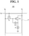
- the gate line GL and the data line DL which cross each other to define the pixel region P, and a switching element Ts, which is connected to the gate line GL and the data line DL, can be further formed in the pixel region P.
- the switching element Ts is connected to the thin film transistor Tr, which is a driving element.
- the power line PL is spaced apart in parallel from the gate line GL or the data line DL, and the thin film transistor Tr can further include the storage capacitor Cst configured to constantly keep a voltage of the gate electrode 430 for one frame.
- a passivation layer 460 is disposed on the source electrode 452 and the drain electrode 454 and covers the thin film transistor Tr over the whole first substrate 402.
- the passivation layer 460 has a drain contact hole 462 that exposes or does not cover the drain electrode 454 of the thin film transistor Tr.
- the OLED D is located on the passivation layer 460.
- the OLED D includes a first electrode 510 that is connected to the drain electrode 454 of the thin film transistor Tr, a second electrode 520 facing the first electrode 510 and an emissive layer 530 disposed between the first and second electrodes 510 and 520.
- a bank layer 464 is disposed on the passivation layer 460 in order to cover edges of the first electrode 510.
- the bank layer 464 exposes or does not cover a center of the first electrode 510 corresponding to each of the red pixel region RP, the green pixel region GP and the blue pixel region BP.
- the bank layer 464 can be omitted.
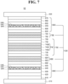
- An emissive layer 530 that can include multiple emitting parts is disposed on the first electrode 510. As illustrated in FIG. 7 as one example, the emissive layer 530 can include multiple emitting parts 600, 700 and 800, and at least one charge generation layer 680 and 780. Each of the emitting parts 600, 700 and 800 includes at least one emitting material layer and can further include an HIL, an HTL, an EBL, an HBL, an ETL and/or an EIL. FIG. 7 will be discussed in more detail later.
- the second electrode 520 can be disposed on the first substrate 402 above which the emissive layer 530 can be disposed.
- the second electrode 520 can be disposed over a whole display area, can include a conductive material with a relatively low work function value compared to the first electrode 510, and can be a cathode.
- the second electrode 520 can include, but is not limited to, highly reflective material such as Al, Mg, Ca, Ag, alloy thereof, and/or combinations thereof such as Al-Mg.
- a color conversion layer can be formed or disposed between the OLED D and the color filter layer 480.
- the color conversion layer can include a red color conversion layer, a green color conversion layer and a blue color conversion layer each of which is disposed correspondingly to each pixel region (RP, GP and BP), respectively, so as to convert the white (W) color light to each of a red, green and blue color lights, respectively.
- the color conversion layer can include quantum dots so that the color purity of the organic light emitting display device 400 can be further improved.
- the organic light emitting display device 400 can comprise the color conversion layer instead of the color filter layer 480.
- the white (W) color light emitted from the OLED D is transmitted through the red color filter pattern 482, the green color filter pattern 484 and the blue color filter pattern 486 each of which is disposed correspondingly to the red pixel region RP, the green pixel region GP and the blue pixel region BP, respectively, so that red, green and blue color lights are displayed in the red pixel region RP, the green pixel region GP and the blue pixel region BP.
- the OLED D2 in accordance with the embodiment of the present invention includes first and second electrodes 510 and 520 and an emissive layer 530 disposed between the first and second electrodes 510 and 520.
- the emissive layer 530 includes a first emitting part 600 disposed between the first and second electrodes 510 and 520, a second emitting part 700 disposed between the first emitting part 600 and the second electrode 520, a third emitting part 800 disposed between the second emitting part 700 and the second electrode 520, a first charge generation layer (CGL1) 680 disposed between the first and second emitting parts 600 and 700, and a second charge generation layer (CGL2) 780 disposed between the second and third emitting parts 700 and 800.
- CGL1 charge generation layer
- CGL2 second charge generation layer
- the first electrode 510 can be an anode and can include a conductive material having relatively high work function value such as TCO.
- the second electrode 520 can be a cathode and can include a conductive material with a relatively low work function value, for example, highly reflective material.
- the second emitting part 700 includes a second emitting material layer (EML2) 740.
- the second emitting part 700 can include at least one of a second hole transport layer (HTL2) 720 disposed between the CGL1 680 and the EMI,2 740 and a second electron transport layer (ETL2) 760 disposed between the EMI,2 740 and the CGL2 780.
- the second emitting part 700 can further include at least one of a second electron blocking layer 730 (EBL2) disposed between the HTL2 720 and the EMI,2 740 and a second hole blocking layer (HBL2) 750 disposed between the EMI,2 740 and the ETL2 760.
- EBL2 second electron blocking layer
- the third emitting part 800 includes a third emitting material layer (EML3) 840.
- the third emitting part 800 can include at least one of a third hole transport layer (HTL3) 820 disposed between the CGL2 780 and the EML3 840, a third electron transport layer (ETL3) 860 disposed between the EML3 840 and the second electrode 520, and an electron injection layer (EIL) 870 disposed between the ETL3 860 and the second electrode 520.
- the third emitting part 800 can further include at least one of a third electron blocking layer (EBL3) 830 disposed between the HTL3 820 and the EML3 840 and a third hole blocking layer (HBL3) 850 disposed between the EML3 840 and the ETL3 860.
- EBL3 electron blocking layer
- the HIL 610 is disposed between the first electrode 510 and the HTL1 620 and improves an interface property between the inorganic first electrode 510 and the organic HTL1 620.
- the HIL 610 can include, but is not limited to, MTDATA, NATA, 1T-NATA, 2T-NATA, CuPc, TCTA, NPB (NPD), DNTPD, HAT-CN, F4-TCNA, F6-TCNNQ, TDAPB, PEDOT/PSS, N-(biphenyl-4-yl)-9,9-dimethyl-N-(4-(9-phenyl-9H-carbazol-3-yl)phenyl)-9H-fluoren-2-amine, NPNPB, TAPC, BPBPA, MgF 2 , CaF 2 and/or combinations thereof.
- the HIL 610 can include the hole transporting material doped with the hole injecting material.
- the HIL 610 can be omitted in compliance of the
- each of the HTL1 620, the HTL2 720 and the HTL3 820 can include, but is not limited to, TPD, NPB (NPD), CBP, DNTPD, BPBPA, NPNPB, Poly-TPD, TFB, TAPC, DCDPA, N-(biphenyl-4-yl)-9,9-dimethyl-N-(4-(9-phenyl-9H-carbazol-3-yl)phenyl)-9H-fluoren-2-amine, N-(biphenyl-4-yl)-N-(4-(9-phenyl-9H-carbazol-3-yl)phenyl)biphenyl-4-amine, N-([1,1'-Biphenyl]-4-yl)-9,9-di
- the ETL1 660, the ETL2 760 and the ETL3 860 can facilitate electron transportation in the first emitting part 600, the second emitting part 700 and the third emitting part 800, respectively.
- each of the ETL1 660, the ETL2 760 and the ETL3 860 can include at least one of an oxadiazole-based compound, a triazole-based compound, a phenanthroline-based compound, a benzoxazole-based compound, a benzothiazole-based compound, a benzimidazole-based compound and a triazine-based compound.
- each of the ETL1 660, the ETL2 760 and the ETL3 860 can include, but is not limited to, Alq 3 , PBD, spiro-PBD, Liq, TPBi, BAlq, Bphen, NBphen, BCP, TAZ, NTAZ, TpPyPB, TmPPPyTz, PFNBr, TPQ, TSPO1, ZADN and/or combinations thereof.
- the EII, 870 is disposed between the second electrode 520 and the ETL3 860, and can improve physical properties of the second electrode 520 and therefore, can enhance the lifespan of the OLED D2.
- the EIL 870 can include, but is not limited to, an alkali metal halide or an alkaline earth metal halide such as LiF, CsF, NaF, BaF 2 and the like, and/or an organometallic Compound such as Liq, lithium benzoate, sodium stearate, and the like.
- Each of the EBL1 630, the EBL2 730 and the EBL3 830 can independently include, but is not limited to, TCTA, Tris[4-(diethylamino)phenyl]amine, N-(biphenyl-4-yl)-9,9-dimethyl-N-(4-(9-phenyl-9H-carbazol-3-yl)phenyl)-9H-fluorene-2-amine, TAPC, MTDATA, mCP, mCBP, CuPc, DNTPD, TDAPB, DCDPA, 2,8-bis(9-phenyl-9H-carbazol-3-yl)dibenzo[b,d]thiophene and/or combinations thereof, respectively.
- TCTA Tris[4-(diethylamino)phenyl]amine
- Each of the HBL1 650, the HBL2 750 and the HBL3 850 can include, but is not limited to, at least one of an oxadiazole-based compound, a triazole-based compound, a phenanthroline-based compound, a benzoxazole-based compound, a benzothiazole-based compound, a benzimidazole-based compound, and a triazine-based compound.
- the CGL1 680 is disposed between the first emitting part 600 and the second emitting part 700.
- the CGL1 680 includes a first N-type CGL (N-CGL1) 682 disposed between the ETL1 660 and the HTL2 720 and a first P-type CGL (P-CGL1) 684 disposed between the N-CGL1 682 and the HTL 720.
- the CGL2 780 is disposed between the second emitting part 700 and the third emitting part 800.
- the CGL2 780 includes a second N-type CGL (N-CGL2) 782 disposed between the ETL2 760 and the HTL3 820 and a second P-type CGL (P-CGL2) 784 disposed between the N-CGL2 782 and the HTL3 820.
- N-CGL2 N-type CGL
- P-CGL2 P-type CGL
- Each of the N-CGL1 682 and the N-CGL2 782 can be an organic layer with electron transporting material doped with an alkali metal such as Li, Na, K and Cs and/or an alkaline earth metal such as Mg, Sr, Ba and Ra.
- an alkali metal such as Li, Na, K and Cs
- an alkaline earth metal such as Mg, Sr, Ba and Ra.
- the contents of the alkali metal and/or the alkaline earth metal in each of the N-CGL1 682 and the N-CGL2 782 can be, but is not limited to, between about 0.1 wt% and about 30 wt%, for example, about 1 wt% and about 10 wt%.
- each of the P-CGL1 684 and the P-CGL2 784 can include, but is not limited to, inorganic material selected from the group consisting of WO x , MoO x , Be 2 O 3 , V 2 O 5 and/or combinations thereof.
- each of the P-CGL1 684 and the P-CGL2 784 can include organic material of the hole transporting material doped with the hole injecting material (e.g., organic material such as HAT-CN, F4-TCNQ and/or F6-TCNNQ and/or inorganic material such as MgF 2 and/or CaF 2 ).
- the contents of the hole injecting material in the P-CGL1 684 and the P-CGL2 784 can be, but is not limited to, between about 2 wt% and about 15 wt%.
- the EML1 (first blue EML) 640 can include a first host 642, a second host 644 and a blue emitter 646.
- the EML3 (second blue EML) 840 can include a first host 842, a second host 844 and a blue emitter 846.
- Each of the first hosts 642 and 842 can be independently the anthracene-based organic compound having the structure of Chemical Formulae 1 to 2
- each of the second hosts 644 and 844 can be independently the anthracene-based organic compound having the structure of Chemical Formulae 3 to 4.
- the HOMO energy level, excited triplet energy level of the first hosts 642 and 842 and the second hosts 644 and 844, and the contents of those hosts in each of the EMI,1 640 and the EML3 840 can be correspondingly identical to those with referring to FIGS. 3 and 5 .
- the hosts 642 and 644 in the EML1 640 can be identical to or different form the hosts 842 and 844 in the EML3 840.
- the blue emitter 646 in the EMI,1 640 can be identical to or different from the blue emitter 846 in the EML3 840.
- the P-type blue host can include, but is not limited to, an aryl/hetero aryl amine-based organic compound substituted with at least one aromatic group and/or hetero aromatic group, a carbazole-based organic compound and/or a spirofluorene-based organic compound.
- the N-type blue host can include an azine-based organic compound and/or a benzimidazole-based organic compound.
- the blue host in the EMI,1 640 can include, but is not limited to, 1,3-Bis(carbazol-9-yl)benzene (mCP), 9-(3-(9H-carbazol-9-yl)phenyl)-9H-carbazole-3-carbonitrile (mCP-CN), mCBP, CBP-CN, 9-(3-(9H-Carbazol-9-yl)phenyl)-3-(diphenylphosphoryl)-9H-carbazole (mCPPO1) 3,5-Di(9H-carbazol-9-yl)biphenyl (Ph-mCP), TSPO1, 9-(3'-(9H-carbazol-9-yl)-[1,1'-biphenyl]-3-yl)-9H-pyrido[2,3-b]indole (CzBPCb), Bis(2-methylphenyl)diphenylsilane (UGH-1), 1,4-Bis(triphenyl
- the contents of the blue host in the EMI,1 640 can be between about 50 wt% and about 99 wt%, for example, about 80 wt% and about 95 wt%. Further, the contents of the blue emitter in the EMI,1 640 can be between about 1 wt% and about 50 wt%, for example, about 5 wt% and about 20 wt%, but is not limited thereto.
- the EMI,1 640 includes both the P-type blue host and the N-type blue host, the P-type blue host and the N-type blue host can be admixed with, but is not limited to, a weight ratio of about 4:1 to about 1:4, for example, about 3:1 to about 1:3.
- At least one of the EMI,1 640 and the EML3 840 can include the first hosts 642 and 842 and the second hosts 644 and 844 with controlled energy level so that the OLED D2 with improved luminous properties can be realized.
- the OLED D2 where the EML3 840 includes two hosts will be described in more detail.
- the P-CGL2 784 can include hole transporting material and a P-type dopant PD.
- the P-type dopant PD takes electrons from the HOMO energy level state of the hole transporting material and induce hole generations in the organic material. Accordingly, the P-type dopant PD has a lowest unoccupied molecular orbital (LUMO) energy level similar to the HOMO energy level of the hole transporting material in the HTL3 820.
- LUMO unoccupied molecular orbital
- the P-type dopant PD in the P-CGL2 784 has a LUMO energy level between about -5.6 eV and -5.7 eV and the hole transporting material in the P-CGL2 784 and the HTL3 820 has a HOMO energy level between about -5.6 eV and about -5.7 eV.
- the electron blocking material in the EBL3 830 has a HOMO energy level between about -5.8 eV in order to transport holes efficiently.
- the host in the conventional EML3 840 has a HOMO energy level around -6.0 eV.
- the holes accumulated in the interface between the conventional EML3 840, and the HTL3 820 and/or the EBL3 830 disposed adjacently to the conventional EML3 840 can cause the hole transporting material and/or the electron blocking material to be deteriorated, and thus, the luminous lifespan of the organic light emitting diode can be reduced.
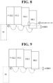
- FIG. 9 illustrates a schematic diagram showing energy levels among a common layer and a blue emitting material layer of the emitting unit adjacently to the cathode in an organic light emitting diode with a tandem structure in accordance with an embodiment of the present invention.
- the energy bandgap ⁇ HOMO4 between the HOMO energy level of the host in the EML3 840 including both the first and second hosts 842 and 844, and the HOMO energy level of the hole transporting material and/or the electron blocking material can be about 0.15 eV or less, for example, about 0.1 eV or less.
- the holes generated at the P-CGL2 784 can be injected rapidly into the blue EML3 840 via the HTL3 820 and the EBL3 830. Since the holes injected efficiently into the blue EML3 840 can be recombined with electrons to generate effective excitons, the luminous efficiency of the OLED D2 can be improved.
- the EMI,2 740 includes a first layer 740A disposed between the EBL2 730 and the HBL2 750, a second layer 740B disposed between the first layer 740A and the HBL2 750, and optionally, a third layer 740C disposed between the first layer 740A and the second layer 740B.
- One of the first layer 740A and the second layer 740B can emit red color light and the other of the first layer 740A and the second layer 740B can emit green color light.
- the OLED D2 where the first layer 740A emits red color light and the second layer 740B emits green color light will be described in more detail.
- the first layer 740A can include a red host and a red emitter (red dopant)
- the second layer 740B can include a green host and a green emitter (green dopant)
- the third layer 740C can include a yellow-green host and a yellow-green emitter (yellow-green dopant).
- the red host can include at least one of a P-type red host and an N-type red host
- the green host can include at least one of a P-type green host and an N-type green host
- the yellow-green host can include at least one of a P-type yellow-green host and an N-type yellow-green host.
- the yellow-green emitter in the third layer 740C can include at least one of yellow-green phosphorescent material, yellow-green fluorescent material and yellow-green delayed fluorescent material.
- the yellow-green emitter can include, but is not limited to, 5,6,11,12-Tetraphenylnaphthalene (Rubrene), 2,8-Di-tert-butyl-5,11-bis(4-tert-butylphenyl)-6,12-diphenyltetracene (TBRb), Bis(2-phenylbenzothiazolato)(acetylacetonate)irdium(III) (Ir(BT) 2 (acac)), Bis(2-(9,9-diethyl-fluoren-2-yl)-1-phenyl-1H-benzo[d]imdiazolato)(acetylacetonate)iridium(III) (Ir(fbi) 2 (acac)), Bis(2-phenylpyridine)(3
- At least one of the EMI,1 640 and the EML3 840 includes the first host 642 or 842 and the seocnd host 644 or 844 so that the OLED D2 with beneficial luminous property can be realized.
- the OLED D2 has a tandem structure so that the color purity and luminous property of the OLED D2 can be further improved.
- Example 1 (Ex. 1): Fabrication of OLED
- Hole injection layer HIL, DNTPD (50 wt%), MgF 2 (50 wt%), 70 ⁇ ); first hole transport layer (HTL1, DNTPD (HOMO: -5.58 eV, LUMO: -2.52 eV), 1000 ⁇ ); first electron blocking layer (EBL1, TCTA (HOMO: -5.8 eV, LUMO: -2.61 eV), 150 ⁇ ); first blue emitting material layer (B-EML1, Host (first host MADN (HOMO: -6.0 eV, LUMO: -3.0 eV) and second host Compound BH2-1 of Chemical Formula 4 (HOMO: -5.8 eV, LUMO: -2.8 eV) by weight ratio of 9:1, 95 wt%), DABNA-1 (5 wt%), 200 ⁇ ); first electron transport layer (ETL1, ZADN, 110 ⁇ ); first N-type charge generation layer (N-CGL1, Bphen (98 wt%), Li
- the fabricated OLED was encapsulated with glass and then transferred from the deposition chamber to a dry box in order to form a film. And then, the OLED was encapsulated with UV-cured epoxy resin and water getter.
- the structures of materials of hole injecting material, hole transporting material, blue emitter, red host, red emitter, yellow-green emitter, green emitter and electron transporting material are illustrated in the following:
- An OLED was fabricated using the same procedure and the same material as Example 1, except that the first host MADN and the second host Compound BH2-1 in the first blue emitting material layer was admixed with a weight ratio of 7:3.
- An OLED where the second blue emitting material layer of the third emitting unit disposed adjacently to the cathode includes a first host and a second host was fabricated.
- the OLED was fabricated using the same procedure and the same material as Example 1, except that the first blue emitting material layer included only the first host MADN (95 wt%) and blue emitter DABNA-1 (5 wt%), and the second emitting material layer included host (first host MADN and the second host Compound BH2-1 by weight ratio 9: 1, 95 wt%) and the blue emitter DABNA-1 (5 wt%).
- Example 5 (Ex. 5): Fabrication of OLEDs
- An OLED was fabricated using the same procedure and the same material as Example 4, except that the first host MADN and the second host Compound BH2-1 in the second blue emitting material layer was admixed with a weight ratio of 8:2.
- Example 6 (Ex. 6): Fabrication of OLEDs
- An OLED was fabricated using the same procedure and the same material as Example 1, except that the first host MADN and the second host Compound BH2-1 in the second blue emitting material layer was admixed with a weight ratio of 7:3.
- An OLED was fabricated using the same procedure and the same material as Example 1, except that both the first blue emitting material layer and the second blue emitting material layer included only the first host MADN (95 wt%) and the blue emitter DABNA-1 ( 5 wt%).
- Each of the OLEDs were connected to an external power source and then luminous properties for all the OLEDs were evaluated using a constant current source (KEITHLEY) and a photometer PR650 at room temperature.
- driving voltage V, relative value
- External quantum efficiency EQE, relative value
- time period LT 95 , relative value
- luminance of the red color light was reduced to 95% from initial luminance was measured at a current density 40 mA/cm 2 and at 40°C.
- the measurement results are indicated in the following Table 1.
- the second blue emitting material layer in the third emitting part which receives holes from the second P-type charge generation layer, disposed adjacently to the cathode, includes the first host and the second host
- luminous lifespan of the OLED was improved significantly.
- the contents of the second host in the blue emitting material layer was designed to be between 10 wt% and 20 wt%, the luminous lifespan can be maximized with maintaining EQE.
- Example 7 Fabrication of OLED
- organic light emitting diode where a blue emitting material layer in a single emitting unit includes a first host and a second host was fabricated.
- organic layer was deposited as the following order:
- Hole injection layer (HIL, DNTPD (80 wt%), P-type dopant (20 wt%), 100 ⁇ ); hole transport layer (HTL, DNTPD, 1000 ⁇ ); electron blocking layer (EBL, TCTA, 50 ⁇ ); blue emitting material layer (B-EML, Host (first host MADN and second host Compound BH2-1 of Chemical Formula 4 by weight ratio of 8:2, 95 wt%), DABNA-1 (5 wt%), 300 ⁇ ); electron transport layer (ETL, ZADN, 200 ⁇ ); electron injection layer (EIL, LIF, 15 ⁇ ); and cathode (Al, 100 ⁇ ).
- An OLED was fabricated using the same procedure and the same material as Example 7, except that Compound BH2-2 (Ex. 8), Compound BH2-3 (Ex. 9), Compound BH2-4 (Ex. 10), Compound BH2-5 (Ex. 11), Compound BH2-6 (Ex. 12) and Compound BH2-7 (Ex. 13) of Chemical Formula 4 instead of Compound BH2-1 as the second host in the blue emitting material was used, respectively.
- An OLED was fabricated using the same procedure and the same material as Example 7, except that both the first blue emitting material layer and the second blue emitting material layer included only the first host MADN (95 wt%) and the blue emitter DABNA-1 ( 5 wt%).
- Example 13 As indicated in Table 2, compared to the OLED fabricated in Comparative Example 2, in the OLEDs fabricated in Examples 7-13, the driving voltage was lowered, and EQE and luminous lifespan was improved significantly. In particular, as in Example 13, when the second host substituted with deuterium was used together with the first host, the luminous lifespan was greatly improved.
Landscapes
- Physics & Mathematics (AREA)
- Optics & Photonics (AREA)
- Chemical & Material Sciences (AREA)
- Engineering & Computer Science (AREA)
- Materials Engineering (AREA)
- Spectroscopy & Molecular Physics (AREA)
- Organic Chemistry (AREA)
- Microelectronics & Electronic Packaging (AREA)
- Electroluminescent Light Sources (AREA)
Applications Claiming Priority (1)
| Application Number | Priority Date | Filing Date | Title |
|---|---|---|---|
| KR1020230006705A KR20240114819A (ko) | 2023-01-17 | 2023-01-17 | 유기발광다이오드 및 유기발광장치 |
Publications (2)
| Publication Number | Publication Date |
|---|---|
| EP4404718A1 true EP4404718A1 (de) | 2024-07-24 |
| EP4404718B1 EP4404718B1 (de) | 2025-12-24 |
Family
ID=87930179
Family Applications (1)
| Application Number | Title | Priority Date | Filing Date |
|---|---|---|---|
| EP23195036.1A Active EP4404718B1 (de) | 2023-01-17 | 2023-09-04 | Organische leuchtdiode und organische lichtemittierende vorrichtung |
Country Status (4)
| Country | Link |
|---|---|
| US (1) | US20240260293A1 (de) |
| EP (1) | EP4404718B1 (de) |
| KR (1) | KR20240114819A (de) |
| CN (1) | CN118368916A (de) |
Families Citing this family (1)
| Publication number | Priority date | Publication date | Assignee | Title |
|---|---|---|---|---|
| CN120152516B (zh) * | 2025-02-19 | 2026-03-13 | 京东方科技集团股份有限公司 | 有机电致发光器件、显示基板和显示装置 |
Citations (5)
| Publication number | Priority date | Publication date | Assignee | Title |
|---|---|---|---|---|
| KR20190139792A (ko) * | 2018-06-08 | 2019-12-18 | 주식회사 엘지화학 | 유기발광소자 |
| US20210184152A1 (en) * | 2019-12-16 | 2021-06-17 | Samsung Display Co., Ltd. | Organic light-emitting device and apparatus including the same |
| US20210320273A1 (en) * | 2020-04-02 | 2021-10-14 | Samsung Display Co., Ltd. | Organic light-emitting device and apparatus including the same |
| US20210384436A1 (en) * | 2018-12-28 | 2021-12-09 | Lg Display Co., Ltd. | Organic light emitting diode and organic light emitting device having thereof |
| US20220393113A1 (en) * | 2020-02-14 | 2022-12-08 | Idemitsu Kosan Co.,Ltd. | Organic electroluminescent element and electronic device |
-
2023
- 2023-01-17 KR KR1020230006705A patent/KR20240114819A/ko active Pending
- 2023-07-11 US US18/220,709 patent/US20240260293A1/en active Pending
- 2023-08-02 CN CN202310965142.0A patent/CN118368916A/zh active Pending
- 2023-09-04 EP EP23195036.1A patent/EP4404718B1/de active Active
Patent Citations (5)
| Publication number | Priority date | Publication date | Assignee | Title |
|---|---|---|---|---|
| KR20190139792A (ko) * | 2018-06-08 | 2019-12-18 | 주식회사 엘지화학 | 유기발광소자 |
| US20210384436A1 (en) * | 2018-12-28 | 2021-12-09 | Lg Display Co., Ltd. | Organic light emitting diode and organic light emitting device having thereof |
| US20210184152A1 (en) * | 2019-12-16 | 2021-06-17 | Samsung Display Co., Ltd. | Organic light-emitting device and apparatus including the same |
| US20220393113A1 (en) * | 2020-02-14 | 2022-12-08 | Idemitsu Kosan Co.,Ltd. | Organic electroluminescent element and electronic device |
| US20210320273A1 (en) * | 2020-04-02 | 2021-10-14 | Samsung Display Co., Ltd. | Organic light-emitting device and apparatus including the same |
Non-Patent Citations (1)
| Title |
|---|
| HYOUNGCHEOL LIM: "Breaking the Efficiency Limit of Deep-Blue Fluorescent OLEDs Based on Anthracene Derivatives", vol. 34, no. 1, 23 October 2021 (2021-10-23), DE, XP093160905, ISSN: 0935-9648, Retrieved from the Internet <URL:https://onlinelibrary.wiley.com/doi/full-xml/10.1002/adma.202100161> DOI: 10.1002/adma.202100161 * |
Also Published As
| Publication number | Publication date |
|---|---|
| EP4404718B1 (de) | 2025-12-24 |
| KR20240114819A (ko) | 2024-07-25 |
| US20240260293A1 (en) | 2024-08-01 |
| CN118368916A (zh) | 2024-07-19 |
Similar Documents
| Publication | Publication Date | Title |
|---|---|---|
| EP4404718B1 (de) | Organische leuchtdiode und organische lichtemittierende vorrichtung | |
| US12581792B2 (en) | Organic light emitting diode and organic light emitting device having thereof | |
| US20240237524A1 (en) | Organic light emitting diode | |
| US20240215288A1 (en) | Organic light emitting diode and organic light emitting device | |
| CN118139441A (zh) | 有机发光二极管 | |
| KR20240070100A (ko) | 유기발광다이오드 및 이를 포함하는 유기발광장치 | |
| EP4408146A1 (de) | Organische leuchtdiode und organische lichtemittierende vorrichtung | |
| EP4391767A1 (de) | Organische leuchtdiode und organische lichtemittierende vorrichtung | |
| US20240268141A1 (en) | Organic light emitting diode and organic light emitting device | |
| US20240224570A1 (en) | Organic light emitting diodes and organic light emitting devices | |
| US20240237517A1 (en) | Organic light emitting diode and organic light emitting device | |
| JP7749633B2 (ja) | 有機発光ダイオード | |
| US20240206330A1 (en) | Organic Light Emitting Diode | |
| US20240215442A1 (en) | Organic light emitting diode and organic light emitting device | |
| KR102861355B1 (ko) | 유기발광다이오드 및 유기발광장치 | |
| US20240081146A1 (en) | Organic light emitting diode and organic light emitting device having thereof | |
| KR20250094757A (ko) | 유기 화합물, 이를 포함하는 유기발광다이오드 및 유기발광장치 | |
| KR20250093837A (ko) | 유기발광다이오드 및 유기발광장치 | |
| KR20250093834A (ko) | 유기발광다이오드 및 유기발광장치 | |
| KR20250093835A (ko) | 유기발광다이오드 및 유기발광장치 | |
| KR20250093836A (ko) | 유기발광다이오드 및 유기발광장치 |
Legal Events
| Date | Code | Title | Description |
|---|---|---|---|
| PUAI | Public reference made under article 153(3) epc to a published international application that has entered the european phase |
Free format text: ORIGINAL CODE: 0009012 |
|
| STAA | Information on the status of an ep patent application or granted ep patent |
Free format text: STATUS: REQUEST FOR EXAMINATION WAS MADE |
|
| 17P | Request for examination filed |
Effective date: 20230904 |
|
| AK | Designated contracting states |
Kind code of ref document: A1 Designated state(s): AL AT BE BG CH CY CZ DE DK EE ES FI FR GB GR HR HU IE IS IT LI LT LU LV MC ME MK MT NL NO PL PT RO RS SE SI SK SM TR |
|
| RBV | Designated contracting states (corrected) |
Designated state(s): AL AT BE BG CH CY CZ DE DK EE ES FI FR GB GR HR HU IE IS IT LI LT LU LV MC ME MK MT NL NO PL PT RO RS SE SI SK SM TR |
|
| RIC1 | Information provided on ipc code assigned before grant |
Ipc: H10K 50/11 20230101ALN20250516BHEP Ipc: H10K 50/19 20230101ALN20250516BHEP Ipc: H10K 85/60 20230101AFI20250516BHEP |
|
| RIC1 | Information provided on ipc code assigned before grant |
Ipc: H10K 85/60 20230101AFI20250612BHEP Ipc: H10K 50/19 20230101ALN20250612BHEP Ipc: H10K 50/11 20230101ALN20250612BHEP |
|
| GRAP | Despatch of communication of intention to grant a patent |
Free format text: ORIGINAL CODE: EPIDOSNIGR1 |
|
| STAA | Information on the status of an ep patent application or granted ep patent |
Free format text: STATUS: GRANT OF PATENT IS INTENDED |
|
| INTG | Intention to grant announced |
Effective date: 20250717 |
|
| GRAS | Grant fee paid |
Free format text: ORIGINAL CODE: EPIDOSNIGR3 |
|
| GRAA | (expected) grant |
Free format text: ORIGINAL CODE: 0009210 |
|
| STAA | Information on the status of an ep patent application or granted ep patent |
Free format text: STATUS: THE PATENT HAS BEEN GRANTED |
|
| AK | Designated contracting states |
Kind code of ref document: B1 Designated state(s): AL AT BE BG CH CY CZ DE DK EE ES FI FR GB GR HR HU IE IS IT LI LT LU LV MC ME MK MT NL NO PL PT RO RS SE SI SK SM TR |
|
| REG | Reference to a national code |
Ref country code: CH Ref legal event code: F10 Free format text: ST27 STATUS EVENT CODE: U-0-0-F10-F00 (AS PROVIDED BY THE NATIONAL OFFICE) Effective date: 20251224 Ref country code: GB Ref legal event code: FG4D |
|
| REG | Reference to a national code |
Ref country code: DE Ref legal event code: R096 Ref document number: 602023010036 Country of ref document: DE |
|
| REG | Reference to a national code |
Ref country code: LT Ref legal event code: MG9D |
|
| PG25 | Lapsed in a contracting state [announced via postgrant information from national office to epo] |
Ref country code: NO Free format text: LAPSE BECAUSE OF FAILURE TO SUBMIT A TRANSLATION OF THE DESCRIPTION OR TO PAY THE FEE WITHIN THE PRESCRIBED TIME-LIMIT Effective date: 20260324 |
|
| PG25 | Lapsed in a contracting state [announced via postgrant information from national office to epo] |
Ref country code: FI Free format text: LAPSE BECAUSE OF FAILURE TO SUBMIT A TRANSLATION OF THE DESCRIPTION OR TO PAY THE FEE WITHIN THE PRESCRIBED TIME-LIMIT Effective date: 20251224 Ref country code: HR Free format text: LAPSE BECAUSE OF FAILURE TO SUBMIT A TRANSLATION OF THE DESCRIPTION OR TO PAY THE FEE WITHIN THE PRESCRIBED TIME-LIMIT Effective date: 20251224 |
|
| PG25 | Lapsed in a contracting state [announced via postgrant information from national office to epo] |
Ref country code: RS Free format text: LAPSE BECAUSE OF FAILURE TO SUBMIT A TRANSLATION OF THE DESCRIPTION OR TO PAY THE FEE WITHIN THE PRESCRIBED TIME-LIMIT Effective date: 20260324 |
|
| PG25 | Lapsed in a contracting state [announced via postgrant information from national office to epo] |
Ref country code: LV Free format text: LAPSE BECAUSE OF FAILURE TO SUBMIT A TRANSLATION OF THE DESCRIPTION OR TO PAY THE FEE WITHIN THE PRESCRIBED TIME-LIMIT Effective date: 20251224 |