EP4404458A1 - Verfahren und techniken zur verbesserung der stabilität von kaskodenverstärkern und zur verbesserung der leitungseffizienz in mehrstufigen leistungsverstärkern - Google Patents
Verfahren und techniken zur verbesserung der stabilität von kaskodenverstärkern und zur verbesserung der leitungseffizienz in mehrstufigen leistungsverstärkern Download PDFInfo
- Publication number
- EP4404458A1 EP4404458A1 EP24151466.0A EP24151466A EP4404458A1 EP 4404458 A1 EP4404458 A1 EP 4404458A1 EP 24151466 A EP24151466 A EP 24151466A EP 4404458 A1 EP4404458 A1 EP 4404458A1
- Authority
- EP
- European Patent Office
- Prior art keywords
- power amplifier
- efficiency
- coupled
- control terminal
- cascode
- Prior art date
- Legal status (The legal status is an assumption and is not a legal conclusion. Google has not performed a legal analysis and makes no representation as to the accuracy of the status listed.)
- Pending
Links
- 238000000034 method Methods 0.000 title claims description 24
- 239000003990 capacitor Substances 0.000 claims abstract description 51
- 230000003071 parasitic effect Effects 0.000 claims abstract description 30
- 238000005516 engineering process Methods 0.000 claims description 10
- 238000004891 communication Methods 0.000 claims description 9
- JMASRVWKEDWRBT-UHFFFAOYSA-N Gallium nitride Chemical compound [Ga]#N JMASRVWKEDWRBT-UHFFFAOYSA-N 0.000 claims description 7
- 229910002601 GaN Inorganic materials 0.000 claims description 6
- 230000008878 coupling Effects 0.000 claims description 2
- 238000010168 coupling process Methods 0.000 claims description 2
- 238000005859 coupling reaction Methods 0.000 claims description 2
- 238000004513 sizing Methods 0.000 claims description 2
- 101000807991 Homo sapiens Testis-specific basic protein Y 1 Proteins 0.000 abstract 2
- 102100038977 Testis-specific basic protein Y 1 Human genes 0.000 abstract 2
- 229910052751 metal Inorganic materials 0.000 description 28
- 239000002184 metal Substances 0.000 description 28
- 101100489713 Saccharomyces cerevisiae (strain ATCC 204508 / S288c) GND1 gene Proteins 0.000 description 14
- 238000010586 diagram Methods 0.000 description 10
- 230000008901 benefit Effects 0.000 description 8
- 230000005669 field effect Effects 0.000 description 5
- 230000006872 improvement Effects 0.000 description 5
- 230000005540 biological transmission Effects 0.000 description 3
- 238000013461 design Methods 0.000 description 3
- 239000000463 material Substances 0.000 description 3
- 238000001465 metallisation Methods 0.000 description 3
- 238000012545 processing Methods 0.000 description 3
- 230000007423 decrease Effects 0.000 description 2
- 230000001419 dependent effect Effects 0.000 description 2
- 238000003780 insertion Methods 0.000 description 2
- 230000037431 insertion Effects 0.000 description 2
- 238000012986 modification Methods 0.000 description 2
- 230000004048 modification Effects 0.000 description 2
- 239000000758 substrate Substances 0.000 description 2
- 101100484930 Saccharomyces cerevisiae (strain ATCC 204508 / S288c) VPS41 gene Proteins 0.000 description 1
- 238000013459 approach Methods 0.000 description 1
- 230000001413 cellular effect Effects 0.000 description 1
- 238000012937 correction Methods 0.000 description 1
- 230000003247 decreasing effect Effects 0.000 description 1
- 230000000694 effects Effects 0.000 description 1
- 230000002708 enhancing effect Effects 0.000 description 1
- 238000002955 isolation Methods 0.000 description 1
- 238000004519 manufacturing process Methods 0.000 description 1
- 238000005259 measurement Methods 0.000 description 1
- 150000002739 metals Chemical class 0.000 description 1
- 238000004806 packaging method and process Methods 0.000 description 1
- 230000008569 process Effects 0.000 description 1
- 230000000087 stabilizing effect Effects 0.000 description 1
Images


Classifications
-
- H—ELECTRICITY
- H03—ELECTRONIC CIRCUITRY
- H03F—AMPLIFIERS
- H03F1/00—Details of amplifiers with only discharge tubes, only semiconductor devices or only unspecified devices as amplifying elements
- H03F1/08—Modifications of amplifiers to reduce detrimental influences of internal impedances of amplifying elements
- H03F1/22—Modifications of amplifiers to reduce detrimental influences of internal impedances of amplifying elements by use of cascode coupling, i.e. earthed cathode or emitter stage followed by earthed grid or base stage respectively
- H03F1/223—Modifications of amplifiers to reduce detrimental influences of internal impedances of amplifying elements by use of cascode coupling, i.e. earthed cathode or emitter stage followed by earthed grid or base stage respectively with MOSFET's
-
- H—ELECTRICITY
- H03—ELECTRONIC CIRCUITRY
- H03F—AMPLIFIERS
- H03F1/00—Details of amplifiers with only discharge tubes, only semiconductor devices or only unspecified devices as amplifying elements
- H03F1/02—Modifications of amplifiers to raise the efficiency, e.g. gliding Class A stages, use of an auxiliary oscillation
- H03F1/0205—Modifications of amplifiers to raise the efficiency, e.g. gliding Class A stages, use of an auxiliary oscillation in transistor amplifiers
- H03F1/0288—Modifications of amplifiers to raise the efficiency, e.g. gliding Class A stages, use of an auxiliary oscillation in transistor amplifiers using a main and one or several auxiliary peaking amplifiers whereby the load is connected to the main amplifier using an impedance inverter, e.g. Doherty amplifiers
-
- H—ELECTRICITY
- H03—ELECTRONIC CIRCUITRY
- H03F—AMPLIFIERS
- H03F1/00—Details of amplifiers with only discharge tubes, only semiconductor devices or only unspecified devices as amplifying elements
- H03F1/08—Modifications of amplifiers to reduce detrimental influences of internal impedances of amplifying elements
- H03F1/22—Modifications of amplifiers to reduce detrimental influences of internal impedances of amplifying elements by use of cascode coupling, i.e. earthed cathode or emitter stage followed by earthed grid or base stage respectively
-
- H—ELECTRICITY
- H03—ELECTRONIC CIRCUITRY
- H03F—AMPLIFIERS
- H03F1/00—Details of amplifiers with only discharge tubes, only semiconductor devices or only unspecified devices as amplifying elements
- H03F1/30—Modifications of amplifiers to reduce influence of variations of temperature or supply voltage or other physical parameters
- H03F1/301—Modifications of amplifiers to reduce influence of variations of temperature or supply voltage or other physical parameters in MOSFET amplifiers
-
- H—ELECTRICITY
- H03—ELECTRONIC CIRCUITRY
- H03F—AMPLIFIERS
- H03F1/00—Details of amplifiers with only discharge tubes, only semiconductor devices or only unspecified devices as amplifying elements
- H03F1/30—Modifications of amplifiers to reduce influence of variations of temperature or supply voltage or other physical parameters
- H03F1/307—Modifications of amplifiers to reduce influence of variations of temperature or supply voltage or other physical parameters in push-pull amplifiers
-
- H—ELECTRICITY
- H03—ELECTRONIC CIRCUITRY
- H03F—AMPLIFIERS
- H03F1/00—Details of amplifiers with only discharge tubes, only semiconductor devices or only unspecified devices as amplifying elements
- H03F1/56—Modifications of input or output impedances, not otherwise provided for
- H03F1/565—Modifications of input or output impedances, not otherwise provided for using inductive elements
-
- H—ELECTRICITY
- H03—ELECTRONIC CIRCUITRY
- H03F—AMPLIFIERS
- H03F3/00—Amplifiers with only discharge tubes or only semiconductor devices as amplifying elements
- H03F3/189—High-frequency amplifiers, e.g. radio frequency amplifiers
- H03F3/19—High-frequency amplifiers, e.g. radio frequency amplifiers with semiconductor devices only
- H03F3/195—High-frequency amplifiers, e.g. radio frequency amplifiers with semiconductor devices only in integrated circuits
-
- H—ELECTRICITY
- H03—ELECTRONIC CIRCUITRY
- H03F—AMPLIFIERS
- H03F3/00—Amplifiers with only discharge tubes or only semiconductor devices as amplifying elements
- H03F3/20—Power amplifiers, e.g. Class B amplifiers, Class C amplifiers
- H03F3/21—Power amplifiers, e.g. Class B amplifiers, Class C amplifiers with semiconductor devices only
- H03F3/211—Power amplifiers, e.g. Class B amplifiers, Class C amplifiers with semiconductor devices only using a combination of several amplifiers
-
- H—ELECTRICITY
- H03—ELECTRONIC CIRCUITRY
- H03F—AMPLIFIERS
- H03F3/00—Amplifiers with only discharge tubes or only semiconductor devices as amplifying elements
- H03F3/20—Power amplifiers, e.g. Class B amplifiers, Class C amplifiers
- H03F3/24—Power amplifiers, e.g. Class B amplifiers, Class C amplifiers of transmitter output stages
- H03F3/245—Power amplifiers, e.g. Class B amplifiers, Class C amplifiers of transmitter output stages with semiconductor devices only
-
- H—ELECTRICITY
- H03—ELECTRONIC CIRCUITRY
- H03F—AMPLIFIERS
- H03F3/00—Amplifiers with only discharge tubes or only semiconductor devices as amplifying elements
- H03F3/30—Single-ended push-pull [SEPP] amplifiers; Phase-splitters therefor
- H03F3/3001—Single-ended push-pull [SEPP] amplifiers; Phase-splitters therefor with field-effect transistors
- H03F3/3022—CMOS common source output SEPP amplifiers
-
- H—ELECTRICITY
- H04—ELECTRIC COMMUNICATION TECHNIQUE
- H04B—TRANSMISSION
- H04B1/00—Details of transmission systems, not covered by a single one of groups H04B3/00 - H04B13/00; Details of transmission systems not characterised by the medium used for transmission
- H04B1/02—Transmitters
- H04B1/04—Circuits
- H04B1/0458—Arrangements for matching and coupling between power amplifier and antenna or between amplifying stages
-
- H—ELECTRICITY
- H03—ELECTRONIC CIRCUITRY
- H03F—AMPLIFIERS
- H03F2200/00—Indexing scheme relating to amplifiers
- H03F2200/451—Indexing scheme relating to amplifiers the amplifier being a radio frequency amplifier
-
- H—ELECTRICITY
- H03—ELECTRONIC CIRCUITRY
- H03F—AMPLIFIERS
- H03F2200/00—Indexing scheme relating to amplifiers
- H03F2200/61—Indexing scheme relating to amplifiers the cascode amplifier has more than one common gate stage
-
- H—ELECTRICITY
- H03—ELECTRONIC CIRCUITRY
- H03F—AMPLIFIERS
- H03F2203/00—Indexing scheme relating to amplifiers with only discharge tubes or only semiconductor devices as amplifying elements covered by H03F3/00
- H03F2203/30—Indexing scheme relating to single-ended push-pull [SEPP]; Phase-splitters therefor
- H03F2203/30084—Indexing scheme relating to single-ended push-pull [SEPP]; Phase-splitters therefor the pull circuit of the SEPP amplifier being a cascode circuit
-
- H—ELECTRICITY
- H03—ELECTRONIC CIRCUITRY
- H03F—AMPLIFIERS
- H03F2203/00—Indexing scheme relating to amplifiers with only discharge tubes or only semiconductor devices as amplifying elements covered by H03F3/00
- H03F2203/30—Indexing scheme relating to single-ended push-pull [SEPP]; Phase-splitters therefor
- H03F2203/30117—Indexing scheme relating to single-ended push-pull [SEPP]; Phase-splitters therefor the push circuit of the SEPP amplifier being a cascode circuit
-
- H—ELECTRICITY
- H04—ELECTRIC COMMUNICATION TECHNIQUE
- H04B—TRANSMISSION
- H04B1/00—Details of transmission systems, not covered by a single one of groups H04B3/00 - H04B13/00; Details of transmission systems not characterised by the medium used for transmission
- H04B1/02—Transmitters
- H04B1/04—Circuits
- H04B2001/0408—Circuits with power amplifiers
- H04B2001/045—Circuits with power amplifiers with means for improving efficiency
Definitions
- the present disclosure relates to multi-stage power amplifiers employed in wireless communications.
- the efficiency of a power amplifier is a key parameter for any communication systems as power amplifiers in a transmitter unit consume a considerable part of the supplied power.
- Thermal conductivity of a package and solid-state material, insertion loss of matching networks, and load impedance are among the main parameters that establish efficiency of a single-stage power amplifier.
- efficiency and gain of each stage determine the overall (lineup) efficiency of a power amplifier. For example, in a two-stage power amplifier, gain and efficiency of the final stage together with efficiency of first stage determine the lineup efficiency. While improving efficiency of each stage has been explored, gain (of last stage, especially) has been overlooked given that there are not too many options available (such as engineering solid-state material).
- the first transistor and the second transistor are field-effect transistors.
- the first current terminal and the third current terminal are source terminals, while the second current terminal and the fourth current terminal are drain terminals.
- the first control terminal and the second control terminal are gate terminals.
- the fixed voltage node is typically ground.
- any of the foregoing aspects individually or together, and/or various separate aspects and features as described herein, may be combined for additional advantage. Any of the various features and elements as disclosed herein may be combined with one or more other disclosed features and elements unless indicated to the contrary herein.
- Embodiments are described herein with reference to schematic illustrations of embodiments of the disclosure. As such, the actual dimensions of the layers and elements can be different, and variations from the shapes of the illustrations as a result, for example, of manufacturing techniques and/or tolerances, are expected. For example, a region illustrated or described as square or rectangular can have rounded or curved features, and regions shown as straight lines may have some irregularity. Thus, the regions illustrated in the figures are schematic and their shapes are not intended to illustrate the precise shape of a region of a device and are not intended to limit the scope of the disclosure. Additionally, sizes of structures or regions may be exaggerated relative to other structures or regions for illustrative purposes and, thus, are provided to illustrate the general structures of the present subject matter and may or may not be drawn to scale. Common elements between figures may be shown herein with common element numbers and may not be subsequently re-described.
- the present disclosure pertains to increasing lineup (overall) efficiency in power amplifiers, including power amplifier modules and integrated circuits, which is commonly perceived as a significant requirement for designing transmitter units for communication and radar applications.
- Methods and techniques disclosed herein result in higher lineup efficiency, at least 4 percentage points in one embodiment, without modifying solid-stage material or sacrificing other key performance parameters such as power and stability.
- the methods and techniques disclosed herein include, but are not limited to, the following considerations:
- FIG. 1 is a schematic of a related-art two-stage power amplifier 10 that has a first stage 12 and a second stage 14 coupled between an RF input terminal 16, labeled RFIN, and an RF output 18, labeled RFOUT.
- the first stage 12 has a first stage gain G1 and a first stage efficiency ⁇ 1
- the second stage 14 has a second stage gain G2 and a second stage efficiency ⁇ 2 .
- CS common source
- CE common emitter
- the cascode transistor formed by the first FET and the second FET, is a gallium nitride (GaN) high electron mobility transistor (HEMT) that has 3 dB to 5 dB higher gain compared with its common source counterpart designed in the same technology and with the same periphery, also known as gate periphery.
- GaN gallium nitride
- HEMT high electron mobility transistor
- the gain of a cascode transistor is determined by class of operation and varies as a function of source and load impedance that are provided to the transistor.
- V G2 of the disclosed cascode power amplifier is configured to achieve maximum gain while output power and drain efficiency are kept close to output power and drain efficiency of a counterpart common source power amplifier with the same solid-state technology.
- the cascode transistor is biased in class AB and load impedances are chosen in such a way as to maximize efficiency of the transistor at maximum power level.
- load impedances are chosen in such a way as to maximize efficiency of the transistor at maximum power level.
- Z OPT the load impedance
- gain that the transistor can deliver is limited to the gain (typically lower than maximum gain) at Z OPT load impedance.
- the cascode FET can still provide 3 dB to 5 dB higher gain compared with a common source FET under the same load and bias conditions.
- the second FET is biased in class C and load impedances are chosen in such a way as to maximize efficiency of transistor at maximum power level.
- load impedances are chosen in such a way as to maximize efficiency of transistor at maximum power level.
- These conditions are identical to a common method used to design auxiliary (peaking) amplifiers for a DPA, and the load impedance is called Z OPT .
- gain that the transistor can deliver is limited to the gain (typically lower than maximum gain) at Z OPT load impedance.
- a cascode FET can still provide 3 dB to 5 dB higher gain compared with a common source FET under the same load and bias conditions.
- the 4B has the first delay circuitry 38 coupled between the first stage 12 and the main cascode amplifier 34, and the second delay circuitry 40 coupled between the auxiliary cascode amplifier 36 and the RF output terminal 18.
- Other common circuitries like splitters, input matching networks, output matching networks, and load modulation networks are not shown for simplicity.
- Second stage or final stage Doherty gain and efficiency at average output power is 18 dB and 55%, respectively, which are optimized by adjusting gate voltage of the common gate FET, in this embodiment VG2, in the cascode structure.
- the first stage 12 implemented using a single-ended common source FET can be replaced by a single-ended cascode FET to achieve higher lineup gain while the same lineup efficiency is maintained.
- the first stage 12 is a single-ended common source FET in FIGS. 4A and 4B and may be replaced by a DPA that uses common source or cascode FETs to achieve even higher lineup efficiency.
- the first stage 12 in the single-ended common source FET may be replaced by a balanced power amplifier that uses common source or cascode FETs to achieve better isolation between the first stage 12 and the second stage 14.
- cascode FETs can be used in the second stage 14 or all stages of a multi-stage power amplifier, such as the two-stage power amplifier 10.
- first stage FET transistors in any examples described above may be replaced by heterojunction bipolar transistors (HBTs).
- cascode power amplifiers with enhanced stability.
- the cascode power amplifiers provide higher gain compared with common source power amplifiers or common emitter power amplifiers.
- higher gain in cascode power amplifiers results in instability issues that make implementing some embodiments relatively more challenging.
- a layout structure at the transistor level to resolve the stability issue of the cascode power amplifiers for a desired frequency band.
- a matching network (not shown in FIG. 3 ) may be needed between the first FET Q1 and the second FET Q2.
- One challenge is that there are parasitic inductances and capacitances between the first FET Q1 and the second FET Q2 and at the second gate GA2 (e.g., L G2 ) which limit available options to improve stability.
- an improved cascode structure for the cascode power amplifier 20 can be realized as unit cells 20-1, 20-2, 20-(N-1), and 20-N, as shown in FIG. 5 , wherein N is a natural counting number.
- each individual unit cell 20-N is a cascode FET.
- Equivalent inductance of L1 through LN and L M1 together with the bypass capacitor C BPY1 form a resonator with resonance frequency in desired operating frequency ranges (e.g., 3.5 GHz to 8 GHz for an 8x325 ⁇ m FET periphery). This typically causes unconditional instability in the same frequency range where the cascode FET oscillates.
- a cascode FET structure and layout to further reduce the parasitic inductance on the second gates, like GA2 of Q 2 , by moving the bypass capacitor C BPY1 substantially closer to the gate of the common gate FET Q2.
- This configuration is repeated in each of the unit cells 20-1 through 20-N, as shown in FIG. 6A .
- Each of capacitors C1 through CN is a bypass capacitor for each of the unit cells 20-1 through 20-N.
- the capacitors C1 through CN each have a capacitance that is less than or equal to the capacitance of the bypass capacitor C BPY1 of FIG. 5 .
- each of the capacitors C1 through CN is configured to keep the capacitance minimal while maintaining proper bypass for the RF signal in the desired frequency range. Therefore, the resonance frequency of the N resonant circuits made up of L1 through LN and C1 through CN at gate of each cascode unit cell FET such as the second gate of common gate FET Q2 is shifted to much higher frequencies, which makes the cascode structure stable in a broader frequency range (e.g., up to 8 GHz for an 8x325 ⁇ m FET periphery).
- the capacitors C1 through CN are placed substantially close to the gates of the common gate transistors such as the FET Q2.
- a bottom plate of the first capacitor C1 is placed substantially on top of source vias or source pads of the common source FET Q1 to minimize inductance between C1 and the fixed voltage node GND1, which in this case is ground.
- GND1 fixed voltage node
- bypass capacitors such as C2 and C3, of adjacent unit cells, such as 20-2 and 20-3, that share same source vias or source pads for common source FETs, Q4 and Q6, can be combined into one capacitor. It is important to minimize inductance between source pads of common source FETs, such as Q1, since it has impact on the stability of the second stage 14. This can be achieved by implementing typical methods such as increasing the number of ground vias, via size, or ground pad size.
- Layouts in FIG. 5 and FIG. 6A are fabricated using GaN technology, and small signal S parameters are measured to compare the stability of two embodiments.
- the output return loss S 22 of both embodiments is shown in Smith charts in FIGS. 7A and 7B .
- the S 22 of the embodiment shown in FIG. 5 is depicted in solid line.
- the S 22 of the embodiment shown in FIG. 6A is depicted in dashed line.
- An indicator for unconditional instability is
- of the disclosed layout remains less than 1 up to 8 GHz, whereas for the embodiment in FIG. 5 ,
- This measurement result shows that the cascode structure using topology in FIG.5 is unconditionally instable from 4 GHz to 8GHz.
- the cascode structure using disclosed topology in FIG. 6A is unconditionally instable at frequencies greater than 8GHz. It clearly shows the improvement in stability of a cascode power amplifier which is achieved by minimizing parasitic components and optimizing bypass capacitance for each unit cell 20-1 to 20-N.
- a cascode FET structure and layout to further improve the stability of the cascode in FIG. 6A by adding a resistor between each of the capacitors C1 through CN and the gate of common gate FETs Q2, Q3, ..., Q i-2 , and Q i-1 .
- This configuration is shown in FIG. 6B .
- a plurality of resistors R 1 , R 2 , R N-1 , and R N improves the stability of cascode amplifiers as it results in an
- FIG. 8A is a simplified schematic of adjacent unit cells 20-1 and 20-2.
- FIG. 8B is a layout diagram of the pair of adjacent unit cells 20-1 and 20-2 that are schematically depicted in FIG. 8A .
- Solid lines in FIG. 8B depict some metallization formed within various layers of the layout.
- FIG. 8B does not show all metallization, such as all gate layers metallization, for simplicity.
- Dashed lines depict capacitor areas, and C1 and C2 are formed by two metal layers on the top and bottom of a dielectric layer with a specific dielectric constant.
- Inductances L1 and L2 are dependent on the length and aspect ratios of the metal that creates the inductances L1 and L2.
- the inductance values for the inductances L1 and L2 are between 2 picohenries (pH) and 10 pH in some embodiments, while in other embodiments the inductance values for L1 and L2 are between 10 pH and 20 pH. In still other embodiments, the inductance values for L1 and L2 are between 20 pH and 40 pH.
- the top metal of capacitor C1 is connected to a metal trace that creates L1 and a metal trace that creates LM1.
- the top metal of capacitor C2 is connected to a metal trace that creates L2 and a metal trace that creates LM1.
- Three source vias S_VIA1 couple the bottom metal of the first capacitor C1 to a metal plane that is the fixed voltage node GND1, and a same via couples the source pad of the common source FET Q1 to a metal plane that is the fixed voltage node GND1.
- one via is used to couple the bottom metal of the first capacitor C1 to a metal plane that is the fixed voltage node GND1.
- two vias are used to couple the bottom metal of the first capacitor C1 to a metal plane that is the fixed voltage node GND1.
- four vias are used to couple the bottom metal of the first capacitor C1 to a metal plane that is the fixed voltage node GND1.
- Another set of three source vias S_VIA2 couples the bottom metal of the second capacitor C2 to the metal plane that is the fixed voltage node GND1, and a same via couples the source pad of the common source FET Q2 to a metal plane that is the fixed voltage node GND1.
- one via is used to couple the bottom metal of the second capacitor C2 to a metal plane that is the fixed voltage node GND1.
- two vias are used to couple the bottom metal of the second capacitor C2 to a metal plane that is the fixed voltage node GND1.
- four vias are used to couple the bottom metal of the second capacitor C2 to a metal plane that is the fixed voltage node GND1.
- Embodiments of the present disclosure place the metals making up the first inductance L1 and the second inductance L2 substantially close to first capacitor C1 and the second capacitor C2, respectively.
- the concepts described above may be implemented in various types of wireless communication devices or user elements 42, such as mobile terminals, smart watches, tablets, computers, navigation devices, access points, and the like that support wireless communications, such as cellular, wireless local area network (WLAN), Bluetooth, and near-field communications.
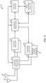
- the user elements 42 will generally include a control system 44, a baseband processor 46, transmit circuitry 48 that includes the cascade power amplifier 20, receive circuitry 50, antenna switching circuitry 52, multiple antennas 54, and user interface circuitry 56.
- the receive circuitry 50 receives radio frequency signals via the antennas 54 and through the antenna switching circuitry 52 from one or more basestations or mobile terminals.
- a low-noise amplifier and a filter cooperate to amplify and remove broadband interference from the received signal for processing.
- Downconversion and digitization circuitry (not shown) then downconvert the filtered, received signal to an intermediate or baseband frequency signal, which is then digitized into one or more digital streams.
- the baseband processor 46 processes the digitized received signal to extract the information or data bits conveyed in the received signal. This processing typically comprises demodulation, decoding, and error correction operations.
- the baseband processor 46 is generally implemented in one or more digital signal processors (DSPs) and application-specific integrated circuits (ASICs).
- DSPs digital signal processors
- ASICs application-specific integrated circuits
- the baseband processor 46 receives digitized data, which may represent voice, data, or control information, from the control system 44, which it encodes for transmission.
- the encoded data are output to the transmit circuitry 48, where they are used by a modulator (not shown) to modulate a carrier signal that is at a desired transmit frequency or frequencies.
- a power amplifier (not shown) amplifies the modulated carrier signal to a level appropriate for transmission and delivers the modulated carrier signal to the antennas 54 through the antenna switching circuitry 52.
- the antennas 54 and the replicated transmit circuitry 48 and receive circuitry 50 may provide spatial diversity. Modulation and processing details will be understood by those skilled in the art.
- a power amplifier cell having a first transistor with a first terminal coupled to ground, a second terminal, and a first control terminal.
- a second transistor has a third terminal coupled to the second terminal, a fourth terminal, and a second control terminal.
- a capacitor having a first plate coupled directly to the second control terminal and a second plate coupled to the ground. As such, there is no intervening inductor component coupled between the first plate and the second control terminal, leaving only parasitic inductance between the first plate and the second control terminal.
- the capacitor has a capacitance sized to resonate with the parasitic inductance at a resonant frequency substantially higher than a desired frequency of operation of the power amplifier cell.
- a power amplifier cell comprising: a first transistor having a first current terminal coupled to a fixed voltage node, a second current terminal, and a first control terminal; a second transistor having a third current terminal coupled to the second current terminal, a fourth current terminal, and a second control terminal; and a capacitor having a first plate coupled directly to the second control terminal and a second plate coupled to the fixed voltage node.
- Clause 5 The power amplifier cell of clause 4 wherein the capacitor has capacitance sized to resonate with the parasitic inductance at a resonant frequency substantially higher than a desired frequency of operation of the power amplifier cell.
- Clause 7 A power amplifier comprising a plurality of the power amplifier cells of any of clauses 1 to 6.
- Clause 12 The power amplifier of clause 11 further comprising a resistor coupled between the parasitic inductance and the first plate.
- Clause 13 The power amplifier of clause 11 or 12 wherein the capacitor has capacitance sized to resonate with the parasitic inductance at a resonant frequency substantially higher than a desired frequency of operation of the power amplifier cell.
- Clause 14 The power amplifier of any of clauses 7 to 13 wherein the fixed voltage node is ground.
- Clause 15 The power amplifier of any of clauses 7 to 14 wherein the first transistor and the second transistor are fabricated of gallium nitride technology.
- a method of realizing enhanced lineup efficiency in an amplifier having a driver stage configured to drive a final stage comprising: implementing a cascode transistor structure within each of a plurality of power amplifier cells comprising the final stage; and minimizing inductance at a gate of each of a common gate transistor comprising the cascode transistor structure by coupling a bypass capacitor directly between each gate and a fixed voltage node.
- Clause 17 The method of realizing enhanced lineup efficiency in an amplifier of clause 16 further comprising sizing capacitance of the bypass capacitor to resonate with a parasitic inductance at a resonant frequency substantially higher than a desired frequency of operation of the amplifier.
- Clause 18 The method of realizing enhanced lineup efficiency in the amplifier of clause 16 or 17 wherein the fixed voltage node is ground.
- a wireless communication device comprising: a baseband processor; transmit circuitry configured to receive encoded data from the baseband processor and to modulate a carrier signal with the encoded data, wherein the transmit circuitry comprises: a first transistor having a first current terminal coupled to a fixed voltage node, a second current terminal, and a first control terminal configured to receive the carrier signal; a second transistor having a third current terminal coupled to the second current terminal, a second control terminal, and a fourth current terminal configured to output an amplified version of the carrier signal; and a capacitor having a first plate coupled directly to the second control terminal and a second plate coupled to the fixed voltage node.
- Clause 21 The wireless device of clause 20 wherein there is no intervening inductor component coupled between the first plate and the second control terminal.
- Clause 22 The wireless device of clause 20 or 21 wherein there is no intervening resistor component coupled between the first plate and the second control terminal.
- Clause 25 The wireless of clause 23 or 24 wherein the capacitor has capacitance sized to resonate with the parasitic inductance at a resonant frequency substantially higher than a desired frequency of operation of the power amplifier cell.
- Clause 26 The wireless device of any of clauses 20 to 25 wherein the fixed voltage node is ground.
Landscapes
- Engineering & Computer Science (AREA)
- Power Engineering (AREA)
- Computer Networks & Wireless Communication (AREA)
- Signal Processing (AREA)
- Microelectronics & Electronic Packaging (AREA)
- Amplifiers (AREA)
Applications Claiming Priority (8)
| Application Number | Priority Date | Filing Date | Title |
|---|---|---|---|
| US202363479788P | 2023-01-13 | 2023-01-13 | |
| US202363479790P | 2023-01-13 | 2023-01-13 | |
| US202363479787P | 2023-01-13 | 2023-01-13 | |
| US202363502268P | 2023-05-15 | 2023-05-15 | |
| US202363511352P | 2023-06-30 | 2023-06-30 | |
| US202363513974P | 2023-07-17 | 2023-07-17 | |
| US202363539384P | 2023-09-20 | 2023-09-20 | |
| US18/400,433 US20240243709A1 (en) | 2023-01-13 | 2023-12-29 | Methods and techniques to improve stability of cascode amplifiers and enhance lineup efficiency in multi-stage power amplifiers |
Publications (1)
| Publication Number | Publication Date |
|---|---|
| EP4404458A1 true EP4404458A1 (de) | 2024-07-24 |
Family
ID=89536021
Family Applications (1)
| Application Number | Title | Priority Date | Filing Date |
|---|---|---|---|
| EP24151466.0A Pending EP4404458A1 (de) | 2023-01-13 | 2024-01-11 | Verfahren und techniken zur verbesserung der stabilität von kaskodenverstärkern und zur verbesserung der leitungseffizienz in mehrstufigen leistungsverstärkern |
Country Status (2)
| Country | Link |
|---|---|
| US (1) | US20240243709A1 (de) |
| EP (1) | EP4404458A1 (de) |
Citations (3)
| Publication number | Priority date | Publication date | Assignee | Title |
|---|---|---|---|---|
| US20030011436A1 (en) * | 2001-07-11 | 2003-01-16 | Fujitsu Limited | Fujitsu limited |
| US20140306761A1 (en) * | 2013-04-16 | 2014-10-16 | Mitsubishi Electric Corporation | Power amplifier |
| US9948252B1 (en) * | 2017-04-06 | 2018-04-17 | Psemi Corporation | Device stack with novel gate capacitor topology |
-
2023
- 2023-12-29 US US18/400,433 patent/US20240243709A1/en active Pending
-
2024
- 2024-01-11 EP EP24151466.0A patent/EP4404458A1/de active Pending
Patent Citations (3)
| Publication number | Priority date | Publication date | Assignee | Title |
|---|---|---|---|---|
| US20030011436A1 (en) * | 2001-07-11 | 2003-01-16 | Fujitsu Limited | Fujitsu limited |
| US20140306761A1 (en) * | 2013-04-16 | 2014-10-16 | Mitsubishi Electric Corporation | Power amplifier |
| US9948252B1 (en) * | 2017-04-06 | 2018-04-17 | Psemi Corporation | Device stack with novel gate capacitor topology |
Also Published As
| Publication number | Publication date |
|---|---|
| US20240243709A1 (en) | 2024-07-18 |
Similar Documents
| Publication | Publication Date | Title |
|---|---|---|
| CN107332517B (zh) | 一种基于增益补偿技术的高线性宽带堆叠低噪声放大器 | |
| CN113114116B (zh) | 一种射频低噪声放大器 | |
| EP3014766B1 (de) | Mmic-leistungsverstärker | |
| US7414478B2 (en) | Integrated parallel power amplifier | |
| CN100413212C (zh) | 高频功率放大器、高频功率放大器模块和便携式电话 | |
| US9698740B2 (en) | Mode linearization switch circuit | |
| JP2012165435A (ja) | 2段のマイクロ波のe級電力増幅器 | |
| CN109245734A (zh) | 一种Ka波段SiGe BiCMOS射频功率放大器 | |
| EP4250559A1 (de) | Leistungsverstärker mit hohem back-off-wirkungsgrad asymmetrisch-gestapelte differentielle quadratur-lastmodulation | |
| CN112087206B (zh) | 一种超低功耗宽带低噪声放大器 | |
| US6614307B1 (en) | Hybrid structure for distributed power amplifiers | |
| US20020125955A1 (en) | Gain and bandwidth enhancement for RF power amplifier package | |
| KR101590605B1 (ko) | 무선 송수신기용 선형 전력증폭기 | |
| WO2023238483A1 (ja) | 増幅回路及び増幅方法 | |
| EP4404458A1 (de) | Verfahren und techniken zur verbesserung der stabilität von kaskodenverstärkern und zur verbesserung der leitungseffizienz in mehrstufigen leistungsverstärkern | |
| Jin et al. | A millimeter-wave power amplifier with 25dB power gain and+ 8dBm saturated output power | |
| CN113131926B (zh) | 一种高线性度幅相控制接收前端电路 | |
| CN118353383A (zh) | 用于提高共源共栅放大器的稳定性并增强多级功率放大器的排列效率的方法和技术 | |
| Singh et al. | CMOS low noise amplifier technologies: trends for enhancing satellite receivers and mobile communications | |
| US10454434B2 (en) | Communication unit | |
| CN113630090A (zh) | 基于无源Balun的宽带高增益高线性度低噪声放大器 | |
| Mehrotra et al. | Design and Analysis of a Broadband Low Noise Amplifier using 0.25 μm GaAs pHEMT Process | |
| Saeeda et al. | Improved Design for the High Gain Wideband Matrix Amplifiers Using Differential Cells and Microwave CMOS Technology | |
| CN117639685A (zh) | 自偏压放大器及mmic放大器芯片 | |
| Agarwal et al. | Design of Ka-Band Power Amplifier and Low-Noise Amplifier for 5G Communication Systems |
Legal Events
| Date | Code | Title | Description |
|---|---|---|---|
| PUAI | Public reference made under article 153(3) epc to a published international application that has entered the european phase |
Free format text: ORIGINAL CODE: 0009012 |
|
| STAA | Information on the status of an ep patent application or granted ep patent |
Free format text: STATUS: THE APPLICATION HAS BEEN PUBLISHED |
|
| AK | Designated contracting states |
Kind code of ref document: A1 Designated state(s): AL AT BE BG CH CY CZ DE DK EE ES FI FR GB GR HR HU IE IS IT LI LT LU LV MC ME MK MT NL NO PL PT RO RS SE SI SK SM TR |
|
| STAA | Information on the status of an ep patent application or granted ep patent |
Free format text: STATUS: REQUEST FOR EXAMINATION WAS MADE |
|
| 17P | Request for examination filed |
Effective date: 20250124 |