EP4404264A1 - Trigger circuit for controlling an esd protection switch - Google Patents
Trigger circuit for controlling an esd protection switch Download PDFInfo
- Publication number
- EP4404264A1 EP4404264A1 EP24152339.8A EP24152339A EP4404264A1 EP 4404264 A1 EP4404264 A1 EP 4404264A1 EP 24152339 A EP24152339 A EP 24152339A EP 4404264 A1 EP4404264 A1 EP 4404264A1
- Authority
- EP
- European Patent Office
- Prior art keywords
- transistor
- terminal
- control terminal
- capacitor
- trigger circuit
- Prior art date
- Legal status (The legal status is an assumption and is not a legal conclusion. Google has not performed a legal analysis and makes no representation as to the accuracy of the status listed.)
- Pending
Links
Images



Classifications
-
- H—ELECTRICITY
- H02—GENERATION; CONVERSION OR DISTRIBUTION OF ELECTRIC POWER
- H02H—EMERGENCY PROTECTIVE CIRCUIT ARRANGEMENTS
- H02H9/00—Emergency protective circuit arrangements for limiting excess current or voltage without disconnection
- H02H9/04—Emergency protective circuit arrangements for limiting excess current or voltage without disconnection responsive to excess voltage
- H02H9/045—Emergency protective circuit arrangements for limiting excess current or voltage without disconnection responsive to excess voltage adapted to a particular application and not provided for elsewhere
- H02H9/046—Emergency protective circuit arrangements for limiting excess current or voltage without disconnection responsive to excess voltage adapted to a particular application and not provided for elsewhere responsive to excess voltage appearing at terminals of integrated circuits
-
- H—ELECTRICITY
- H02—GENERATION; CONVERSION OR DISTRIBUTION OF ELECTRIC POWER
- H02H—EMERGENCY PROTECTIVE CIRCUIT ARRANGEMENTS
- H02H9/00—Emergency protective circuit arrangements for limiting excess current or voltage without disconnection
- H02H9/04—Emergency protective circuit arrangements for limiting excess current or voltage without disconnection responsive to excess voltage
-
- H—ELECTRICITY
- H10—SEMICONDUCTOR DEVICES; ELECTRIC SOLID-STATE DEVICES NOT OTHERWISE PROVIDED FOR
- H10D—INORGANIC ELECTRIC SEMICONDUCTOR DEVICES
- H10D89/00—Aspects of integrated devices not covered by groups H10D84/00 - H10D88/00
- H10D89/60—Integrated devices comprising arrangements for electrical or thermal protection, e.g. protection circuits against electrostatic discharge [ESD]
- H10D89/601—Integrated devices comprising arrangements for electrical or thermal protection, e.g. protection circuits against electrostatic discharge [ESD] for devices having insulated gate electrodes, e.g. for IGFETs or IGBTs
- H10D89/811—Integrated devices comprising arrangements for electrical or thermal protection, e.g. protection circuits against electrostatic discharge [ESD] for devices having insulated gate electrodes, e.g. for IGFETs or IGBTs using FETs as protective elements
- H10D89/819—Bias arrangements for gate electrodes of FETs, e.g. RC networks or voltage partitioning circuits
-
- H—ELECTRICITY
- H02—GENERATION; CONVERSION OR DISTRIBUTION OF ELECTRIC POWER
- H02H—EMERGENCY PROTECTIVE CIRCUIT ARRANGEMENTS
- H02H9/00—Emergency protective circuit arrangements for limiting excess current or voltage without disconnection
- H02H9/04—Emergency protective circuit arrangements for limiting excess current or voltage without disconnection responsive to excess voltage
- H02H9/043—Protection of over-voltage protection device by short-circuiting
-
- H—ELECTRICITY
- H03—ELECTRONIC CIRCUITRY
- H03K—PULSE TECHNIQUE
- H03K17/00—Electronic switching or gating, i.e. not by contact-making and –breaking
- H03K17/51—Electronic switching or gating, i.e. not by contact-making and –breaking characterised by the components used
- H03K17/56—Electronic switching or gating, i.e. not by contact-making and –breaking characterised by the components used by the use, as active elements, of semiconductor devices
-
- H—ELECTRICITY
- H10—SEMICONDUCTOR DEVICES; ELECTRIC SOLID-STATE DEVICES NOT OTHERWISE PROVIDED FOR
- H10D—INORGANIC ELECTRIC SEMICONDUCTOR DEVICES
- H10D89/00—Aspects of integrated devices not covered by groups H10D84/00 - H10D88/00
- H10D89/60—Integrated devices comprising arrangements for electrical or thermal protection, e.g. protection circuits against electrostatic discharge [ESD]
- H10D89/601—Integrated devices comprising arrangements for electrical or thermal protection, e.g. protection circuits against electrostatic discharge [ESD] for devices having insulated gate electrodes, e.g. for IGFETs or IGBTs
- H10D89/811—Integrated devices comprising arrangements for electrical or thermal protection, e.g. protection circuits against electrostatic discharge [ESD] for devices having insulated gate electrodes, e.g. for IGFETs or IGBTs using FETs as protective elements
- H10D89/817—FETs in a Darlington configuration
Definitions
- the present disclosure generally relates to electrostatic discharge, ESD, protection. Particular embodiments relate to a trigger circuit for controlling an ESD protection switch.
- ESD protection scheme must not interfere with the normal operation of the product.
- One method to protect the die is to use active ESD protection. When the voltage of the input terminal rises due to the ESD current, the input of a controlling circuit remains low due to an RC low pass filter. Thus, a PMOS or NMOS turns on allowing an NMOS or PMOS ESD protection switch respectively to turn on. Active ESD protection is advantageous as its operation can be simulated with circuit simulation tools. However, the conventional solution does not leave the gate floating after the ESD event.
- the second diode function is connected in series between the input terminal and one of the two conduction terminals of the first transistor.
- the control terminal of the first transistor is coupled via the first capacitor to the input terminal, such that a rising voltage at the input terminal due to an ESD event triggers the control terminal of the first transistor to activate the conduction path between the two conduction terminals of the first transistor.
- the first capacitor is arranged to be discharged through the first resistor to the output terminal such that, when the first capacitor is discharged below a first threshold of the first transistor, the control terminal of the first transistor deactivates the conduction path between the two conduction terminals of the first transistor.
- a diode function being biased from a first element to a second element may be taken to mean that a diode of the diode function is oriented such that the anode of the diode is directed towards the first element and the cathode of the diode is directed towards the second element. It is noted that this does not necessarily exclude that other, specified or unspecified elements may be present between the anode and the first element or between the cathode and the second element. Moreover, and more generally, if a device is connected in series between a first element and a second element, this does not necessarily exclude that other, specified or unspecified elements may be present between the device and either or both of the first element and the second element. It is up to the skilled person to safeguard that these other, specified or unspecified elements do not disturb the essential function of the described elements.
- a relationship between a charge capacity of the first capacitor and the first threshold of the first transistor and a gate capacitance of the first transistor is configured to keep the first transistor activated for at least a duration of the ESD. In this manner, the first transistor can be activated (i.e. turned on) for the duration of the ESD event, and can thus adequately deal with the ESD.
- the first transistor is a laterally-diffused metal-oxide semiconductor, LDMOS,; or an extended drain field-effect transistor, EDFET.
- the first transistor is a laterally-diffused n-channel metal-oxide semiconductor, LDnMOS; or an n-channel extended drain field-effect transistor, EDFET.
- ESD protection switch comprises a transistor having a maximum drain-to-source voltage rating of substantially 18 V; and/or a maximum gate-to-source voltage rating of substantially 5.5 V.
- substantially may be taken to mean “within at least 20% of”.
- the first capacitor has a charge capacity of at least 18 V.
- the output terminal is configured to float when the conduction path between the two conduction terminals of the first transistor is deactivated.
- the second diode function is implemented using a separate second diode, and the first capacitor is connected to a cathode of the separate second diode.
- the trigger circuit comprises: a second transistor having two conduction terminals and a control terminal; wherein the two conduction terminals of the second transistor are arranged in parallel with the second diode function and wherein the control terminal of the second transistor is configured for controlling a conduction path between the two conduction terminals of the second transistor; and a second timer circuit.
- the second timer circuit comprises: a second resistor connected in series between the control terminal of the second transistor and the input terminal; and a second capacitor connected in series between the control terminal of the second transistor and the input terminal, and connected in parallel with the second resistor.
- the control terminal of the second transistor is connected via the first capacitor to the control terminal of the first transistor.
- the control terminal of the second transistor is coupled via the second capacitor to the input terminal, such that a rising voltage at the input terminal due to an ESD event triggers the control terminal of the second transistor to activate the conduction path between the two conduction terminals of the first transistor.
- the second capacitor is arranged to be discharged through the second resistor to the input terminal such that, when the second capacitor is discharged below a second threshold of the second transistor, the control terminal of the second transistor deactivates the conduction path between the two conduction terminals of the second transistor.
- a relationship between a charge capacity of the second capacitor and the second threshold of the second transistor is configured to keep the first transistor activated for at least a duration of the ESD.
- the second transistor is a laterally-diffused metal-oxide semiconductor, LDMOS; or an extended drain field-effect transistor, EDFET.
- the second transistor is a laterally-diffused n-channel metal-oxide semiconductor, LDnMOS; or an n-channel extended drain field-effect transistor, EDFET.
- the first diode function is implemented using a parasitic diode of the first transistor.
- the second diode function is implemented using a parasitic diode of the second transistor.
- the present disclosure relates to a high-voltage trigger circuit for use in eFuse (electronic fuse), load switch or ideal diode applications, or in any other application with a large n-channel FET between two pins.
- eFuse electronic fuse
- load switch load switch
- ideal diode applications or in any other application with a large n-channel FET between two pins.
- HBM Human Body Model
- MM Machine Model
- the large pass FET Field Effect Transistor
- ESD Electrostatic Discharge
- the gate of the FET should be left floating, allowing it to be driven by other (non-ESD) circuits.
- the ESD protection switch will be turned on using the trigger circuit. Note that for ESD zaps from output to input, the parasitic body-drain diode will conduct the HBM current. When there's an HBM zap between input and output, the ESD protection switch is used to conduct the ESD current. A trigger circuit is needed which will not interfere with the normal operation of the ESD protection device. In regular operation, input can be at 12 V and gate can be pumped to 17 V, so this is a design constraint. When the ESD protection switch is on, the input and output can be at 12 V, the gate will be at 17 V.
- the input can be at 12 V and the output (and gate) can be at any voltage from 0 V to 12 V.
- the trigger circuit In normal mode, the trigger circuit must leave the gate of the ESD protection switch floating so it can be driven by a driver circuit (e.g. attached to terminal 427).
- the gate of the ESD protection switch can be higher or lower than the drain (IN) - the trigger circuit must be able to tolerate this.
- the ESD protection switch is a low-Ohmic device.
- the FET width (and therefore silicon area) is very large.
- FIG 1 schematically illustrates a first embodiment of a trigger circuit 100 according to the present disclosure, which is suitable for controlling an electrostatic discharge, ESD, protection switch (not shown in Figure 1 , but analogous to switch 422 in Figure 4 ).
- the trigger circuit 100 comprises:
- the first diode function 102 and the second diode function 101 may in other words be arranged in a back-to-back configuration, such that they share terminals 115 and 114 of the first transistor and the second transistor.
- first diode function 102 and the second diode function 101 may be implemented using a parasitic diode, i.e. the diode function inherently present in the transistor, or either or both may be implemented using a separate diode arranged in parallel with this parasitic diode. In either case, the arrangement achieves a "diode function".
- the trigger circuit 100 of Figure 1 may additionally comprise the following components, which the skilled person will appreciate to be optional in view of the second and third embodiment as shown in Figures 2 and 3 :
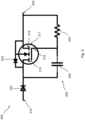
- FIG. 2 schematically illustrates a second embodiment of a trigger circuit 200 according to the present disclosure.
- the trigger circuit of Figure 2 is similar to that of Figure 1 , except in that the function of the second transistor 113 of Figure 1 has been taken over by the second diode function 201 wherein the second diode function 201 is implemented using a separate second diode 201, in such a way that the first capacitor 206 is connected to a cathode of the separate second diode 201.
- the FET may return to the off-state when the ESD event is over.
- FIG 3 schematically illustrates a third embodiment of a trigger circuit 300 according to the present disclosure.
- the trigger circuit of Figure 3 is similar to that of Figure 1 , except in that the function of the second transistor 113 of Figure 1 has been taken over by the second diode function 301 wherein the second diode function 301 is implemented using a separate second diode 301, in such a way that the first capacitor 306 is connected to an anode of the separate second diode 301.
- the FET may return to the off-state when the ESD event is over.
- Figure 4 schematically illustrates an electronic device 419 comprising an ESD protection switch and a fourth embodiment of a trigger circuit 400 according to the present disclosure.
- the trigger circuit 400 may for example be analogous to trigger circuit 100 of Figure 1 , or to trigger circuit 200 of Figure 2 , or to trigger circuit of Figure 3 , or to other, similar trigger circuits within the ambit of the trigger circuit according to the present disclosure.
- Trigger circuit 400 comprises an input terminal 410 arranged to be connected with a first conduction terminal 421 of the ESD protection switch 422; and an output terminal 403 arranged to control a control terminal 423 of the ESD protection switch 422.
- the first conduction terminal 421 of the ESD protection switch 422 and the input terminal 410 of the trigger circuit 400 are electrically connected to the input 420 of the electronic device 419, which is usually denoted as V CC .
- HBM Human Body Model
- ESD Electrostatic Discharge
- the control terminal 423 (gate) of the ESD protection switch 422 is shorted to the Vcc node 420, thus activating the ESD protection switch. Without this feature, the buildup voltage on the first conduction terminal 421 (drain) of the ESD protection switch 422 might rise above the maximum rating of the FET and permanent damage could occur. When V GS of the FET is above the threshold voltage, the FET will turn on and conduct the ESD current. Because Mx is used during the product's normal operation, the trigger circuit must leave the gate floating in 'normal mode'. This will allow the gate 423 to be driven by other (non-ESD) circuits.
- the voltage of the Vcc node 420 will rise quickly, while the second conduction terminal 424 (source) of the ESD protection switch 422 is grounded to ground 425.
- first embodiment 100 of Figure 1 As well as to the fourth embodiment of Figure 4 , where appropriate.
- the voltage at the control terminal 116 of the first transistor 117 and at the control terminal 112 of the optional second transistor 113 will also rise quickly.
- the first transistor 117 will turn on when its gate-to-source voltage rises above a threshold voltage, so V GS,117 > V th,117 .
- the control terminal 112 of the second transistor 113 is coupled high through the second capacitor 108.
- the control terminal 116 of the first transistor 117 is also coupled high through the capacitor 106.
- the first transistor 117 conducts when the control terminal voltage 116 is above a threshold voltage.
- the second transistor 113 conducts when the control terminal voltage 112 is above a threshold voltage.
- the first capacitor 106 is preferably a high voltage capacitor, as the voltage across this capacitor can become very high. In an example implementation, it can be as high as 18 V.
- the Vcc node 420 and the output terminal 403 of the trigger circuit 400 are shorted together, and the control terminal 423 (gate) of the ESD protection switch 422 rises. Because the transconductance gm of the ESD protection switch 422 is very large (as the FET width (and therefore silicon area) is very large), the control terminal 423 (gate) does not need to rise by much for all the HBM current to be shunted.
- a first and second timer circuit 105, 107 are connected to the control terminals 112, 116 of the first 117 and second 113 transistors, and are dimensioned to ensure that the first 117 and second 113 transistors remain on for the duration of the HBM event.
- V GS of the first 117 and second 113 transistors are both 0 (the resistors 104, 109 ensure this). In that case, there is no conduction path between the input terminal 110 and the output terminal 103.
- the control terminal 423 (gate) of the ESD protection switch 422 can now be driven by other non-ESD circuits.
- the first 117 and second 113 transistors may be used to short the gate 423 and drain 421 of the ESD protection switch 422 when an ESD event occurs.
- the gate 423 and drain 421 are fully independent and can have a voltage over the following ranges:
- the large voltage difference between the two nodes means that the first 117 and second 113 transistors are preferably LDMOS devices. Because V(gate 423) can be large or smaller than V(drain 421), back-to-back LDMOS devices are preferred. This is to prevent body-drain diodes from forward biasing since LDMOS devices always have the body and source connected.
- the transistors can also be other types of devices, but the device chosen should be able to withstand high voltage drops across it (e.g. a voltage drop of 18 V). For example an extended drain field-effect transistor (EDFET) can also be used. These have the same voltage limitations as LDMOS devices.
- EFET extended drain field-effect transistor
- the voltage range of drain 421 can be from 0 to 12 V
- the voltage range of gate 423 can be from 0 to V(drain 421) + 5 V.
- the second transistor 113 does not need to be an HV (High Voltage) device. When the eFuse is on, gate 423 is 5 V above drain 421, therefore there won't be more than 5 V across the second transistor 113.
- V(drain 421) 0 to 5 V and V(gate 423) is 0 to V(drain 421) + 5 V
- lower voltage devices can be used (e.g. 5 V devices, as this is the maximum of V gs , V dd , V ds ).
- first and second timer circuits may function as two separate timers: when the voltage at drain 421 (equal to the voltage at node 420) rises, the voltages at the control terminals 116 and 112 of the first 117 and second 113 transistors also rise through the first 106 and second 108 capacitors. After dealing with the ESD event, the voltage at the control terminal 112 of the second transistor 113 will drop to the voltage at the input terminal 110, which is equal to the voltage at drain 421, due to the second resistor 109, and the voltage at the control terminal 116 of the first transistor 117 will also drop to the voltage at the output terminal 103, which is equal to the voltage at gate 423, due to the first resistor 104.
Landscapes
- Engineering & Computer Science (AREA)
- Microelectronics & Electronic Packaging (AREA)
- Semiconductor Integrated Circuits (AREA)
- Metal-Oxide And Bipolar Metal-Oxide Semiconductor Integrated Circuits (AREA)
Abstract
- an input terminal arranged to be connected with a first conduction terminal of the ESD protection switch;
- an output terminal arranged to control a control terminal of the ESD protection switch;
- a first diode function biased from the output terminal to the input terminal ;
- a second diode function biased from the input terminal to the output terminal and connected in series with the first diode function ;
- a first transistor having two conduction terminals and a control terminal; wherein the two conduction terminals of the first transistor are arranged in parallel with the first diode function and wherein the control terminal of the first transistor is configured for controlling a conduction path between the two conduction terminals of the first transistor;
- a first timer circuit comprising:
- a first resistor connected in series between the control terminal of the first transistor and the output terminal ;
- a first capacitor connected in series between the control terminal of the first transistor and the input terminal ;
wherein the second diode function is connected in series between the input terminal and one of the two conduction terminals of the first transistor;
wherein the control terminal of the first transistor is coupled via the first capacitor to the input terminal, such that a rising voltage at the input terminal due to an ESD event triggers the control terminal of the first transistor to activate the conduction path between the two conduction terminals of the first transistor; and
wherein the first capacitor is arranged to be discharged through the first resistor to the output terminal such that, when the first capacitor is discharged below a first threshold of the first transistor, the control terminal of the first transistor deactivates the conduction path between the two conduction terminals of the first transistor.
Description
- The present disclosure generally relates to electrostatic discharge, ESD, protection. Particular embodiments relate to a trigger circuit for controlling an ESD protection switch.
- During an ESD HBM event current must be shunted between pins without overstressing any devices in the path. This can be achieved by placing either dedicated protection devices or by utilizing existing devices to safely shunt the current The ESD protection scheme must not interfere with the normal operation of the product. One method to protect the die is to use active ESD protection. When the voltage of the input terminal rises due to the ESD current, the input of a controlling circuit remains low due to an RC low pass filter. Thus, a PMOS or NMOS turns on allowing an NMOS or PMOS ESD protection switch respectively to turn on. Active ESD protection is advantageous as its operation can be simulated with circuit simulation tools. However, the conventional solution does not leave the gate floating after the ESD event.
- Therefore, it is an aim of at least some embodiments according to the present disclosure to ensure that the ESD protection gate can be left floating after the ESD event.
- Accordingly, there is provided in a first aspect according to the present disclosure a trigger circuit for controlling an electrostatic discharge, ESD, protection switch. The trigger circuit comprises: an input terminal arranged to be connected with a first conduction terminal of the ESD protection switch; an output terminal arranged to control a control terminal of the ESD protection switch; a first diode function biased from the output terminal to the input terminal; a second diode function biased from the input terminal to the output terminal and connected in series with the first diode function; a first transistor having two conduction terminals and a control terminal; wherein the two conduction terminals of the first transistor are arranged in parallel with the first diode function and wherein the control terminal of the first transistor is configured for controlling a conduction path between the two conduction terminals of the first transistor; and a first timer circuit comprising: a first resistor connected in series between the control terminal of the first transistor and the output terminal; a first capacitor connected in series between the control terminal of the first transistor and the input terminal.
- The second diode function is connected in series between the input terminal and one of the two conduction terminals of the first transistor. The control terminal of the first transistor is coupled via the first capacitor to the input terminal, such that a rising voltage at the input terminal due to an ESD event triggers the control terminal of the first transistor to activate the conduction path between the two conduction terminals of the first transistor. The first capacitor is arranged to be discharged through the first resistor to the output terminal such that, when the first capacitor is discharged below a first threshold of the first transistor, the control terminal of the first transistor deactivates the conduction path between the two conduction terminals of the first transistor.
- In this context, a diode function being biased from a first element to a second element may be taken to mean that a diode of the diode function is oriented such that the anode of the diode is directed towards the first element and the cathode of the diode is directed towards the second element. It is noted that this does not necessarily exclude that other, specified or unspecified elements may be present between the anode and the first element or between the cathode and the second element. Moreover, and more generally, if a device is connected in series between a first element and a second element, this does not necessarily exclude that other, specified or unspecified elements may be present between the device and either or both of the first element and the second element. It is up to the skilled person to safeguard that these other, specified or unspecified elements do not disturb the essential function of the described elements.
- In an embodiment, a relationship between a charge capacity of the first capacitor and the first threshold of the first transistor and a gate capacitance of the first transistor is configured to keep the first transistor activated for at least a duration of the ESD. In this manner, the first transistor can be activated (i.e. turned on) for the duration of the ESD event, and can thus adequately deal with the ESD.
- In an embodiment, the first transistor is a laterally-diffused metal-oxide semiconductor, LDMOS,; or an extended drain field-effect transistor, EDFET. In a preferred embodiment, the first transistor is a laterally-diffused n-channel metal-oxide semiconductor, LDnMOS; or an n-channel extended drain field-effect transistor, EDFET.
- In an embodiment, ESD protection switch comprises a transistor having a maximum drain-to-source voltage rating of substantially 18 V; and/or a maximum gate-to-source voltage rating of substantially 5.5 V. In this context, "substantially" may be taken to mean "within at least 20% of".
- In an embodiment, the first capacitor has a charge capacity of at least 18 V.
- In an embodiment, the output terminal is configured to float when the conduction path between the two conduction terminals of the first transistor is deactivated.
- In an embodiment, the second diode function is implemented using a separate second diode, and the first capacitor is connected to a cathode of the separate second diode.
- In another embodiment, the second diode function is implemented using a separate second diode, and the first capacitor is connected to an anode of the separate second diode.
- In yet another embodiment, the trigger circuit comprises: a second transistor having two conduction terminals and a control terminal; wherein the two conduction terminals of the second transistor are arranged in parallel with the second diode function and wherein the control terminal of the second transistor is configured for controlling a conduction path between the two conduction terminals of the second transistor; and a second timer circuit. The second timer circuit comprises: a second resistor connected in series between the control terminal of the second transistor and the input terminal; and a second capacitor connected in series between the control terminal of the second transistor and the input terminal, and connected in parallel with the second resistor. The control terminal of the second transistor is connected via the first capacitor to the control terminal of the first transistor. The control terminal of the second transistor is coupled via the second capacitor to the input terminal, such that a rising voltage at the input terminal due to an ESD event triggers the control terminal of the second transistor to activate the conduction path between the two conduction terminals of the first transistor. The second capacitor is arranged to be discharged through the second resistor to the input terminal such that, when the second capacitor is discharged below a second threshold of the second transistor, the control terminal of the second transistor deactivates the conduction path between the two conduction terminals of the second transistor.
- In an embodiment, a relationship between a charge capacity of the second capacitor and the second threshold of the second transistor is configured to keep the first transistor activated for at least a duration of the ESD.
- In an embodiment, the second transistor is a laterally-diffused metal-oxide semiconductor, LDMOS; or an extended drain field-effect transistor, EDFET. In a preferred embodiment, the second transistor is a laterally-diffused n-channel metal-oxide semiconductor, LDnMOS; or an n-channel extended drain field-effect transistor, EDFET.
- In an embodiment, the first diode function is implemented using a parasitic diode of the first transistor.
- In an embodiment, the second diode function is implemented using a parasitic diode of the second transistor.
- It will be understood that the above-described embodiments are intended merely to illustrate the principles of the present disclosure, and are not intended to be interpreted in a limiting manner. The present disclosure will be more fully understood with the help of the following description and the appended drawings, in which:
-
Figure 1 schematically illustrates a first embodiment of a trigger circuit according to the present disclosure; -
Figure 2 schematically illustrates a second embodiment of a trigger circuit according to the present disclosure; -
Figure 3 schematically illustrates a third embodiment of a trigger circuit according to the present disclosure; and -
Figure 4 schematically illustrates an electronic device comprising an ESD protection switch and a fourth embodiment of a trigger circuit according to the present disclosure. - The present disclosure relates to a high-voltage trigger circuit for use in eFuse (electronic fuse), load switch or ideal diode applications, or in any other application with a large n-channel FET between two pins. When an HBM (Human Body Model) or MM (Machine Model) event occurs between the input and output, the large pass FET (Field Effect Transistor) is turned on thus protecting it. Thus the ESD (Electrostatic Discharge) current is shunted from the input to the output of the device without damage occurring. During 'normal' operation, the gate of the FET should be left floating, allowing it to be driven by other (non-ESD) circuits. To protect against ESD zaps from input to output of the device, the ESD protection switch will be turned on using the trigger circuit. Note that for ESD zaps from output to input, the parasitic body-drain diode will conduct the HBM current. When there's an HBM zap between input and output, the ESD protection switch is used to conduct the ESD current. A trigger circuit is needed which will not interfere with the normal operation of the ESD protection device. In regular operation, input can be at 12 V and gate can be pumped to 17 V, so this is a design constraint. When the ESD protection switch is on, the input and output can be at 12 V, the gate will be at 17 V. When the ESD protection switch is off, the input can be at 12 V and the output (and gate) can be at any voltage from 0 V to 12 V. In normal mode, the trigger circuit must leave the gate of the ESD protection switch floating so it can be driven by a driver circuit (e.g. attached to terminal 427). The gate of the ESD protection switch can be higher or lower than the drain (IN) - the trigger circuit must be able to tolerate this.
- In some embodiments, there is provided an ESD high-voltage trigger circuit for self-protecting FETs. The trigger circuit will turn on the FET when there's an HBM event but will leave the gate floating during normal mode. This will allow the gate to be driven by other non-ESD circuits (e.g. gate driver or charge-pump). The duration that the transistor or transistors will be kept on is easily adjustable by changing the resistor and capacitor values in the circuit. The trigger circuit may in particular be used when the FET's gate can be high or lower than the drain for normal mode. The trigger circuit is applicable for high-voltage or low-voltage applications. The trigger circuit can be simulated with circuit simulation tools (e.g., HSPICE, Spectre) and can be easily implemented in different technologies.
- The ESD protection switch is a low-Ohmic device. The FET width (and therefore silicon area) is very large.
-
Figure 1 schematically illustrates a first embodiment of atrigger circuit 100 according to the present disclosure, which is suitable for controlling an electrostatic discharge, ESD, protection switch (not shown inFigure 1 , but analogous to switch 422 inFigure 4 ). Thetrigger circuit 100 comprises: - an
input terminal 110 arranged to be connected with a first conduction terminal of the ESD protection switch; - an
output terminal 103 arranged to control a control terminal of the ESD protection switch; - a
first diode function 102 biased from theoutput terminal 103 to theinput terminal 110; - a
second diode function 101 biased from theinput terminal 110 to theoutput terminal 103 and connected in series with thefirst diode function 102; - a
first transistor 117 having twoconduction terminals control terminal 116; wherein the twoconduction terminals first transistor 117 are arranged in parallel with thefirst diode function 102 and wherein thecontrol terminal 116 of thefirst transistor 117 is configured for controlling a conduction path between the twoconduction terminals first transistor 117; - a
first timer circuit 105 comprising: - a
first resistor 104 connected in series between thecontrol terminal 116 of thefirst transistor 117 and theoutput terminal 103; - a
first capacitor 106 connected in series between thecontrol terminal 116 of thefirst transistor 117 and theinput terminal 110; - wherein the
second diode function 101 is connected in series between theinput terminal 110 and one of the twoconduction terminals 115 of thefirst transistor 117; - wherein the
control terminal 116 of thefirst transistor 117 is coupled via thefirst capacitor 106 to the input terminal 110 (of course there may be other elements in between thefirst capacitor 106 and the input terminal 110), such that a rising voltage at theinput terminal 110 due to an ESD event triggers thecontrol terminal 116 of thefirst transistor 117 to activate the conduction path between the twoconduction terminals first transistor 117; and - wherein the
first capacitor 106 is arranged to be discharged through thefirst resistor 104 to theoutput terminal 103 such that, when thefirst capacitor 106 is discharged below a first threshold of thefirst transistor 117, thecontrol terminal 116 of thefirst transistor 117 deactivates the conduction path between the twoconduction terminals first transistor 117. - The
first diode function 102 and thesecond diode function 101 may in other words be arranged in a back-to-back configuration, such that they shareterminals - It is noted that either or both of the
first diode function 102 and thesecond diode function 101 may be implemented using a parasitic diode, i.e. the diode function inherently present in the transistor, or either or both may be implemented using a separate diode arranged in parallel with this parasitic diode. In either case, the arrangement achieves a "diode function". - The
trigger circuit 100 ofFigure 1 may additionally comprise the following components, which the skilled person will appreciate to be optional in view of the second and third embodiment as shown inFigures 2 and3 : - a
second transistor 113 having twoconduction terminals control terminal 112; wherein the twoconduction terminals second transistor 113 are arranged in parallel with thesecond diode function 101 and wherein thecontrol terminal 112 of thesecond transistor 113 is configured for controlling a conduction path between the twoconduction terminals second transistor 113; and - a
second timer circuit 107; - a
second resistor 109 connected in series between thecontrol terminal 112 of thesecond transistor 113 and theinput terminal 110; and - a
second capacitor 108 connected in series between thecontrol terminal 112 of thesecond transistor 113 and theinput terminal 110, and connected in parallel with thesecond resistor 109; - wherein the
control terminal 112 of thesecond transistor 113 is connected via thefirst capacitor 106 to thecontrol terminal 116 of thefirst transistor 117; - wherein the
control terminal 112 of thesecond transistor 113 is coupled via thesecond capacitor 108 to theinput terminal 110, such that a rising voltage at theinput terminal 110 due to an ESD event triggers thecontrol terminal 112 of thesecond transistor 113 to activate the conduction path between the twoconduction terminals first transistor 113; and - wherein the
second capacitor 108 is arranged to be discharged through thesecond resistor 109 to theinput terminal 110 such that, when thesecond capacitor 108 is discharged below a second threshold of thesecond transistor 113, thecontrol terminal 112 of thesecond transistor 113 deactivates the conduction path between the twoconduction terminals second transistor 113. -
Figure 2 schematically illustrates a second embodiment of atrigger circuit 200 according to the present disclosure. The trigger circuit ofFigure 2 is similar to that ofFigure 1 , except in that the function of thesecond transistor 113 ofFigure 1 has been taken over by thesecond diode function 201 wherein thesecond diode function 201 is implemented using a separatesecond diode 201, in such a way that thefirst capacitor 206 is connected to a cathode of the separatesecond diode 201. Here too, the FET may return to the off-state when the ESD event is over. -
Figure 3 schematically illustrates a third embodiment of atrigger circuit 300 according to the present disclosure. The trigger circuit ofFigure 3 is similar to that ofFigure 1 , except in that the function of thesecond transistor 113 ofFigure 1 has been taken over by thesecond diode function 301 wherein thesecond diode function 301 is implemented using a separatesecond diode 301, in such a way that thefirst capacitor 306 is connected to an anode of the separatesecond diode 301. Here too, the FET may return to the off-state when the ESD event is over. -
Figure 4 schematically illustrates anelectronic device 419 comprising an ESD protection switch and a fourth embodiment of atrigger circuit 400 according to the present disclosure. Thetrigger circuit 400 may for example be analogous to triggercircuit 100 ofFigure 1 , or to triggercircuit 200 ofFigure 2 , or to trigger circuit ofFigure 3 , or to other, similar trigger circuits within the ambit of the trigger circuit according to the present disclosure. -
Trigger circuit 400 comprises aninput terminal 410 arranged to be connected with afirst conduction terminal 421 of theESD protection switch 422; and anoutput terminal 403 arranged to control acontrol terminal 423 of theESD protection switch 422. - The
first conduction terminal 421 of theESD protection switch 422 and theinput terminal 410 of thetrigger circuit 400 are electrically connected to theinput 420 of theelectronic device 419, which is usually denoted as VCC. - An HBM (Human Body Model) ESD (Electrostatic Discharge) 426 is modelled via a 100 pF capacitor connected to ground, connected in series to a switch, connected in series to a 1.5 kΩ resistor. Of course, the details of this
model 426 are not intended to limit the embodiments according to the present disclosure. - During an HBM event between
Vcc 420 and thesecond conduction terminal 424 of theESD protection switch 422, the control terminal 423 (gate) of theESD protection switch 422 is shorted to theVcc node 420, thus activating the ESD protection switch. Without this feature, the buildup voltage on the first conduction terminal 421 (drain) of theESD protection switch 422 might rise above the maximum rating of the FET and permanent damage could occur. When VGS of the FET is above the threshold voltage, the FET will turn on and conduct the ESD current. Because Mx is used during the product's normal operation, the trigger circuit must leave the gate floating in 'normal mode'. This will allow thegate 423 to be driven by other (non-ESD) circuits. - During an HBM event between the
Vcc node 420 and theoutput node 425 of theelectronic device 419, the voltage of theVcc node 420 will rise quickly, while the second conduction terminal 424 (source) of theESD protection switch 422 is grounded toground 425. - For the following operation of an embodiment according to the present disclosure, reference will be made to the
first embodiment 100 ofFigure 1 as well as to the fourth embodiment ofFigure 4 , where appropriate. Through capacitor coupling of thefirst capacitor 106 and the optionalsecond capacitor 108, the voltage at thecontrol terminal 116 of thefirst transistor 117 and at thecontrol terminal 112 of the optionalsecond transistor 113 will also rise quickly. Thefirst transistor 117 will turn on when its gate-to-source voltage rises above a threshold voltage, so VGS,117 > Vth,117. - During an ESD event the
input terminal 110 rises quickly. Thecontrol terminal 112 of thesecond transistor 113 is coupled high through thesecond capacitor 108. In addition, thecontrol terminal 116 of thefirst transistor 117 is also coupled high through thecapacitor 106. Thefirst transistor 117 conducts when thecontrol terminal voltage 116 is above a threshold voltage. Thesecond transistor 113 conducts when thecontrol terminal voltage 112 is above a threshold voltage. In addition there will be current conduction through thesecond diode function 101. When the ESD event is over, thefirst capacitor 106 is discharged through thefirst resistor 104 to theoutput terminal 103. In parallel thesecond capacitor 108 is discharged through thesecond resistor 109 to theinput terminal 110. Thus Vgs113=0 & VGS117 = 0 and there is no conduction path between theinput terminal 110 and theoutput terminal 103 of the trigger circuit. Thefirst capacitor 106 is preferably a high voltage capacitor, as the voltage across this capacitor can become very high. In an example implementation, it can be as high as 18 V. TheVcc node 420 and theoutput terminal 403 of thetrigger circuit 400 are shorted together, and the control terminal 423 (gate) of theESD protection switch 422 rises. Because the transconductance gm of theESD protection switch 422 is very large (as the FET width (and therefore silicon area) is very large), the control terminal 423 (gate) does not need to rise by much for all the HBM current to be shunted. - A first and
second timer circuit control terminals - The
input terminal 110 and thecontrol terminal 112 of thesecond transistor 113 are shorted when the HBM event has finished (VGS,113 = 0). The output terminal 103 (connectable to thecontrol terminal 423 of theESD protection switch 422, as shown inFigure 4 ) and thecontrol terminal 116 of thefirst transistor 117 are shorted when the HBM event has finished (VGS,117 = 0). - During normal mode, VGS of the first 117 and second 113 transistors are both 0 (the
resistors input terminal 110 and theoutput terminal 103. The control terminal 423 (gate) of theESD protection switch 422 can now be driven by other non-ESD circuits. - The first 117 and second 113 transistors may be used to short the
gate 423 and drain 421 of theESD protection switch 422 when an ESD event occurs. Thegate 423 and drain 421 are fully independent and can have a voltage over the following ranges: - Drain 421: 0 V → 18 V.
- Gate 423: 0 V A V(drain 421) + 5 V.
- The large voltage difference between the two nodes (
gate 423 and drain 421) means that the first 117 and second 113 transistors are preferably LDMOS devices. Because V(gate 423) can be large or smaller than V(drain 421), back-to-back LDMOS devices are preferred. This is to prevent body-drain diodes from forward biasing since LDMOS devices always have the body and source connected. However, the transistors can also be other types of devices, but the device chosen should be able to withstand high voltage drops across it (e.g. a voltage drop of 18 V). For example an extended drain field-effect transistor (EDFET) can also be used. These have the same voltage limitations as LDMOS devices. - In a first specific context, the voltage range of
drain 421 can be from 0 to 12 V, and the voltage range ofgate 423 can be from 0 to V(drain 421) + 5 V. Thefirst transistor 117 is therefore required to be high voltage - when the eFuse is off, V(drain 421) = 12 V and V(gate 423) = 0 V, there will be approximately 12 V across this FET. Thesecond transistor 113 does not need to be an HV (High Voltage) device. When the eFuse is on,gate 423 is 5 V abovedrain 421, therefore there won't be more than 5 V across thesecond transistor 113. In general, for low voltage applications where V(drain 421) = 0 to 5 V and V(gate 423) is 0 to V(drain 421) + 5 V, lower voltage devices can be used (e.g. 5 V devices, as this is the maximum of Vgs, Vdd, Vds). - If these diodes were forward biased, there would be a connection between
drain 421 andgate 423, and they would not be independent. It is desirable to drivegate 423 higher than thesource 424 of theESD protection switch 422. If the diodes are betweengate 423 and drain 421 (that is, diodes facing left in the orientation ofFigure 4 ), the internal driver trying to pull thegate 423 high would be fighting against external supply fromdrain 421. It will not be able to pull up more than two diode drops above the voltage ofdrain 421. In addition, ifdrain 421 is high and theESD protection switch 422 needs to be turned off,gate 423 should be pulled low (so Vgs of theESD protection switch 422 is 0 V). This would be impossible if the diodes are betweendrain 421 and gate 423 (that is, diodes facing right in the orientation ofFigure 4 ) because the internal pull-down ongate 423 would be fighting against external supply fromdrain 421, and drain 421 would win. - It is noted that the first and second timer circuits may function as two separate timers: when the voltage at drain 421 (equal to the voltage at node 420) rises, the voltages at the
control terminals control terminal 112 of thesecond transistor 113 will drop to the voltage at theinput terminal 110, which is equal to the voltage atdrain 421, due to thesecond resistor 109, and the voltage at thecontrol terminal 116 of thefirst transistor 117 will also drop to the voltage at theoutput terminal 103, which is equal to the voltage atgate 423, due to thefirst resistor 104. -
- 100
- trigger circuit
- 101
- second diode function
- 102
- first diode function
- 103
- output terminal
- 104
- first resistor
- 105
- first timer circuit
- 106
- first capacitor
- 107
- second timer circuit
- 108
- second capacitor
- 109
- second resistor
- 110
- input terminal
- 111
- first conduction terminal of second transistor
- 112
- control terminal of second transistor
- 113
- second transistor
- 114
- second conduction terminal of second transistor
- 115
- first conduction terminal of first transistor
- 116
- control terminal of first transistor
- 117
- first transistor
- 118
- second conduction terminal of first transistor
- 200
- trigger circuit
- 201
- second diode function
- 202
- first diode function
- 203
- output terminal
- 204
- first resistor
- 205
- first timer circuit
- 206
- first capacitor
- 210
- input terminal
- 215
- first conduction terminal of first transistor
- 216
- control terminal of first transistor
- 217
- first transistor
- 218
- second conduction terminal of first transistor
- 300
- trigger circuit
- 301
- second diode function
- 302
- first diode function
- 303
- output terminal
- 304
- first resistor
- 305
- first timer circuit
- 306
- first capacitor
- 310
- input terminal
- 315
- first conduction terminal of first transistor
- 316
- control terminal of first transistor
- 317
- first transistor
- 318
- second conduction terminal of first transistor
- 400
- trigger circuit
- 403
- output terminal
- 410
- input terminal
- 419
- electronic device
- 420
- Vcc node
- 421
- first conduction terminal of the ESD protection switch
- 422
- ESD protection switch
- 423
- control terminal of the ESD protection switch
- 424
- second conduction terminal of the ESD protection switch
- 425
- output node of the electronic device (connected to ground)
- 426
- Human Body Model (HBM) Electrostatic Discharge (ESD) model
- 427
- terminal for attaching a driver circuit of the electronic device
Claims (13)
- A trigger circuit for controlling an electrostatic discharge, ESD, protection switch; the trigger circuit comprising:- an input terminal arranged to be connected with a first conduction terminal of the ESD protection switch;- an output terminal arranged to control a control terminal of the ESD protection switch;- a first diode function biased from the output terminal to the input terminal;- a second diode function biased from the input terminal to the output terminal and connected in series with the first diode function;- a first transistor having two conduction terminals and a control terminal; wherein the two conduction terminals of the first transistor are arranged in parallel with the first diode function and wherein the control terminal of the first transistor is configured for controlling a conduction path between the two conduction terminals of the first transistor;- a first timer circuit comprising:- a first resistor connected in series between the control terminal of the first transistor and the output terminal;- a first capacitor connected in series between the control terminal of the first transistor and the input terminal;wherein the second diode function is connected in series between the input terminal and one of the two conduction terminals of the first transistor;wherein the control terminal of the first transistor is coupled via the first capacitor to the input terminal, such that a rising voltage at the input terminal due to an ESD event triggers the control terminal of the first transistor to activate the conduction path between the two conduction terminals of the first transistor; andwherein the first capacitor is arranged to be discharged through the first resistor to the output terminal such that, when the first capacitor is discharged below a first threshold of the first transistor, the control terminal of the first transistor deactivates the conduction path between the two conduction terminals of the first transistor.
- The trigger circuit of claim 1, wherein a relationship between a charge capacity of the first capacitor and the first threshold of the first transistor and a gate capacitance of the first transistor is configured to keep the first transistor activated for at least a duration of the ESD.
- The trigger circuit of any one preceding claim, wherein the first transistor is a laterally-diffused metal-oxide semiconductor, LDMOS, preferably a laterally-diffused n-channel metal-oxide semiconductor, LDnMOS; or an extended drain field-effect transistor, EDFET.
- The trigger circuit of any one preceding claim, wherein ESD protection switch comprises a transistor having a maximum drain-to-source voltage rating of substantially 18 V; and/or a maximum gate-to-source voltage rating of substantially 5.5 V.
- The trigger circuit of any one preceding claim, wherein the first capacitor has a charge capacity of at least 18 V.
- The trigger circuit of any one preceding claim, wherein the output terminal is configured to float when the conduction path between the two conduction terminals of the first transistor is deactivated.
- The trigger circuit of any one preceding claim, wherein the second diode function is implemented using a separate second diode, and wherein the first capacitor is connected to a cathode of the separate second diode.
- The trigger circuit of any one of the claims 1-6, wherein the second diode function is implemented using a separate second diode, and wherein the first capacitor is connected to an anode of the separate second diode.
- The trigger circuit of any one of the claims 1-6, wherein the trigger circuit comprises:- a second transistor having two conduction terminals and a control terminal; wherein the two conduction terminals of the second transistor are arranged in parallel with the second diode function and wherein the control terminal of the second transistor is configured for controlling a conduction path between the two conduction terminals of the second transistor; and- a second timer circuit;wherein the second timer circuit comprises:- a second resistor connected in series between the control terminal of the second transistor and the input terminal; and- a second capacitor connected in series between the control terminal of the second transistor and the input terminal, and connected in parallel with the second resistor; wherein the control terminal of the second transistor is connected via the first capacitor to the control terminal of the first transistor;wherein the control terminal of the second transistor is coupled via the second capacitor to the input terminal, such that a rising voltage at the input terminal due to an ESD event triggers the control terminal of the second transistor to activate the conduction path between the two conduction terminals of the first transistor; andwherein the second capacitor is arranged to be discharged through the second resistor to the input terminal such that, when the second capacitor is discharged below a second threshold of the second transistor, the control terminal of the second transistor deactivates the conduction path between the two conduction terminals of the second transistor.
- The trigger circuit of any one preceding claim, wherein a relationship between a charge capacity of the second capacitor and the second threshold of the second transistor is configured to keep the first transistor activated for at least a duration of the ESD.
- The trigger circuit of any one preceding claim, wherein the second transistor is a laterally-diffused metal-oxide semiconductor, LDMOS, preferably a laterally-diffused n-channel metal-oxide semiconductor, LDnMOS; or an extended drain field-effect transistor, EDFET.
- The trigger circuit of any one preceding claim, wherein the first diode function is implemented using a parasitic diode of the first transistor.
- The trigger circuit of any one preceding claim when dependent on claim 9, wherein the second diode function is implemented using a parasitic diode of the second transistor.
Applications Claiming Priority (1)
| Application Number | Priority Date | Filing Date | Title |
|---|---|---|---|
| US202363480125P | 2023-01-17 | 2023-01-17 |
Publications (1)
| Publication Number | Publication Date |
|---|---|
| EP4404264A1 true EP4404264A1 (en) | 2024-07-24 |
Family
ID=89620666
Family Applications (1)
| Application Number | Title | Priority Date | Filing Date |
|---|---|---|---|
| EP24152339.8A Pending EP4404264A1 (en) | 2023-01-17 | 2024-01-17 | Trigger circuit for controlling an esd protection switch |
Country Status (3)
| Country | Link |
|---|---|
| US (1) | US20240243569A1 (en) |
| EP (1) | EP4404264A1 (en) |
| CN (1) | CN118367524A (en) |
Citations (2)
| Publication number | Priority date | Publication date | Assignee | Title |
|---|---|---|---|---|
| US20070230073A1 (en) * | 2006-04-04 | 2007-10-04 | Ming-Dou Ker | High-voltage tolerant power-rail esd clamp circuit |
| US20130234199A1 (en) * | 2010-12-28 | 2013-09-12 | Industrial Technology Research Institute | ESD Protection Circuit |
Family Cites Families (1)
| Publication number | Priority date | Publication date | Assignee | Title |
|---|---|---|---|---|
| CN109193601B (en) * | 2018-09-25 | 2020-04-21 | 华为技术有限公司 | An ESD protection circuit |
-
2024
- 2024-01-16 CN CN202410059951.XA patent/CN118367524A/en active Pending
- 2024-01-17 US US18/414,888 patent/US20240243569A1/en active Pending
- 2024-01-17 EP EP24152339.8A patent/EP4404264A1/en active Pending
Patent Citations (2)
| Publication number | Priority date | Publication date | Assignee | Title |
|---|---|---|---|---|
| US20070230073A1 (en) * | 2006-04-04 | 2007-10-04 | Ming-Dou Ker | High-voltage tolerant power-rail esd clamp circuit |
| US20130234199A1 (en) * | 2010-12-28 | 2013-09-12 | Industrial Technology Research Institute | ESD Protection Circuit |
Non-Patent Citations (1)
| Title |
|---|
| YIQUN CAO ET AL: "Statically triggered active ESD clamps for high-voltage applications", ELECTRICAL OVERSTRESS/ELECTROSTATIC DISCHARGE SYMPOSIUM (EOS/ESD), 2012 34TH, IEEE, 9 September 2012 (2012-09-09), pages 1 - 10, XP032254972, ISBN: 978-1-4673-1467-1 * |
Also Published As
| Publication number | Publication date |
|---|---|
| CN118367524A (en) | 2024-07-19 |
| US20240243569A1 (en) | 2024-07-18 |
Similar Documents
| Publication | Publication Date | Title |
|---|---|---|
| US7706113B1 (en) | Electrical overstress (EOS) and electrostatic discharge (ESD) protection circuit and method of use | |
| US10468870B2 (en) | Electrostatic protection circuit | |
| US6529359B1 (en) | Circuits for dynamic turn off of NMOS output drivers during EOS/ESD stress | |
| US9130562B2 (en) | Active ESD protection circuit | |
| US6970336B2 (en) | Electrostatic discharge protection circuit and method of operation | |
| US7626790B2 (en) | Electrostatic discharge protection for a circuit capable of handling high input voltage | |
| US7203045B2 (en) | High voltage ESD power clamp | |
| US20140368957A1 (en) | Electrostatic protection circuit | |
| EP3520191B1 (en) | Esd protection charge pump active clamp for low-leakage applications | |
| US20150214732A1 (en) | Semiconductor circuit | |
| JP6708989B2 (en) | Electrostatic discharge protection device and circuit device | |
| US20080106834A1 (en) | electrostatic discharge protection circuit | |
| US8345396B2 (en) | Electrostatic discharge protectors having increased RC delays | |
| US10069297B2 (en) | Electrostatic protection circuit | |
| US20200243512A1 (en) | Nmos transistor with bulk dynamically coupled to drain | |
| US8059376B2 (en) | ESD clamp for high voltage operation | |
| US20240243569A1 (en) | Trigger Circuit for Controlling an ESD Protection Switch | |
| JP5613488B2 (en) | Overvoltage protection circuit | |
| US7518845B2 (en) | RC-triggered power clamp suppressing negative mode electrostatic discharge stress | |
| US20230154919A1 (en) | Protection of a domain of an integrated circuit against overvoltages | |
| US20250380514A1 (en) | Clamping arrangements and clamping circuits | |
| US20160064920A1 (en) | Auxiliary self-protecting transistor structure | |
| US20250169194A1 (en) | Electrostatic discharge protection circuit |
Legal Events
| Date | Code | Title | Description |
|---|---|---|---|
| PUAI | Public reference made under article 153(3) epc to a published international application that has entered the european phase |
Free format text: ORIGINAL CODE: 0009012 |
|
| STAA | Information on the status of an ep patent application or granted ep patent |
Free format text: STATUS: THE APPLICATION HAS BEEN PUBLISHED |
|
| AK | Designated contracting states |
Kind code of ref document: A1 Designated state(s): AL AT BE BG CH CY CZ DE DK EE ES FI FR GB GR HR HU IE IS IT LI LT LU LV MC ME MK MT NL NO PL PT RO RS SE SI SK SM TR |
|
| STAA | Information on the status of an ep patent application or granted ep patent |
Free format text: STATUS: REQUEST FOR EXAMINATION WAS MADE |
|
| 17P | Request for examination filed |
Effective date: 20250124 |
|
| REG | Reference to a national code |
Ref country code: DE Ref legal event code: R079 Free format text: PREVIOUS MAIN CLASS: H01L0027020000 Ipc: H10D0089600000 |
|
| GRAP | Despatch of communication of intention to grant a patent |
Free format text: ORIGINAL CODE: EPIDOSNIGR1 |
|
| STAA | Information on the status of an ep patent application or granted ep patent |
Free format text: STATUS: GRANT OF PATENT IS INTENDED |
|
| RIC1 | Information provided on ipc code assigned before grant |
Ipc: H10D 89/60 20250101AFI20260216BHEP Ipc: H02H 9/04 20060101ALI20260216BHEP |
|
| INTG | Intention to grant announced |
Effective date: 20260302 |