EP4404222A2 - Mehrschichtiges keramisches elektronisches bauelement, das in seinem mittleren teil ein molverhältnis von in/(ni+in) von 0,002 oder mehr aufweist, das 70 % oder mehr beträgt - Google Patents
Mehrschichtiges keramisches elektronisches bauelement, das in seinem mittleren teil ein molverhältnis von in/(ni+in) von 0,002 oder mehr aufweist, das 70 % oder mehr beträgt Download PDFInfo
- Publication number
- EP4404222A2 EP4404222A2 EP24151136.9A EP24151136A EP4404222A2 EP 4404222 A2 EP4404222 A2 EP 4404222A2 EP 24151136 A EP24151136 A EP 24151136A EP 4404222 A2 EP4404222 A2 EP 4404222A2
- Authority
- EP
- European Patent Office
- Prior art keywords
- internal electrodes
- points
- electronic component
- multilayer electronic
- dielectric
- Prior art date
- Legal status (The legal status is an assumption and is not a legal conclusion. Google has not performed a legal analysis and makes no representation as to the accuracy of the status listed.)
- Pending
Links
Images


Classifications
-
- H—ELECTRICITY
- H01—ELECTRIC ELEMENTS
- H01G—CAPACITORS; CAPACITORS, RECTIFIERS, DETECTORS, SWITCHING DEVICES, LIGHT-SENSITIVE OR TEMPERATURE-SENSITIVE DEVICES OF THE ELECTROLYTIC TYPE
- H01G4/00—Fixed capacitors; Processes of their manufacture
- H01G4/30—Stacked capacitors
-
- H—ELECTRICITY
- H01—ELECTRIC ELEMENTS
- H01G—CAPACITORS; CAPACITORS, RECTIFIERS, DETECTORS, SWITCHING DEVICES, LIGHT-SENSITIVE OR TEMPERATURE-SENSITIVE DEVICES OF THE ELECTROLYTIC TYPE
- H01G4/00—Fixed capacitors; Processes of their manufacture
- H01G4/002—Details
- H01G4/005—Electrodes
- H01G4/008—Selection of materials
- H01G4/0085—Fried electrodes
-
- H—ELECTRICITY
- H01—ELECTRIC ELEMENTS
- H01G—CAPACITORS; CAPACITORS, RECTIFIERS, DETECTORS, SWITCHING DEVICES, LIGHT-SENSITIVE OR TEMPERATURE-SENSITIVE DEVICES OF THE ELECTROLYTIC TYPE
- H01G4/00—Fixed capacitors; Processes of their manufacture
- H01G4/002—Details
- H01G4/005—Electrodes
- H01G4/012—Form of non-self-supporting electrodes
-
- H—ELECTRICITY
- H01—ELECTRIC ELEMENTS
- H01G—CAPACITORS; CAPACITORS, RECTIFIERS, DETECTORS, SWITCHING DEVICES, LIGHT-SENSITIVE OR TEMPERATURE-SENSITIVE DEVICES OF THE ELECTROLYTIC TYPE
- H01G4/00—Fixed capacitors; Processes of their manufacture
- H01G4/002—Details
- H01G4/018—Dielectrics
- H01G4/06—Solid dielectrics
- H01G4/08—Inorganic dielectrics
- H01G4/12—Ceramic dielectrics
- H01G4/1209—Ceramic dielectrics characterised by the ceramic dielectric material
- H01G4/1218—Ceramic dielectrics characterised by the ceramic dielectric material based on titanium oxides or titanates
- H01G4/1227—Ceramic dielectrics characterised by the ceramic dielectric material based on titanium oxides or titanates based on alkaline earth titanates
Definitions
- the present disclosure relates to a multilayer electronic component.
- a Multilayer Ceramic Capacitor a multilayer electronic component, is a chip-type condenser mounted on printed circuit boards of various electronic products, for example, video devices such as liquid crystal displays (LCDs), plasma display panels (PDPs) and the like, computers, smartphones, and mobile phones, serving to charge or discharge electricity therein.
- video devices such as liquid crystal displays (LCDs), plasma display panels (PDPs) and the like, computers, smartphones, and mobile phones, serving to charge or discharge electricity therein.
- LCDs liquid crystal displays
- PDPs plasma display panels
- Multilayer ceramic capacitors may be used as components in various electronic devices due to having a small size, high capacitance, and ease of installation. As various electronic devices such as computers and mobile devices are miniaturized and have higher output, demand for miniaturization and higher capacitance for multilayer ceramic capacitors is increasing.
- An aspect of the present disclosure is to provide a multilayer electronic component having relatively high reliability.
- An aspect of the present disclosure is to provide a multilayer electronic component having improved capacitance.
- An aspect of the present disclosure is to provide a multilayer electronic component having excellent high temperature load lifespan.
- An aspect of the present disclosure is to suppress a phenomenon of internal electrode agglomeration and internal electrode disconnection.
- An aspect of the present disclosure is to improve a distribution of capacitance and grain size.
- An aspect of the present disclosure is to improve a distribution of insulation resistance.
- a multilayer electronic component includes a body including a plurality of dielectric layers and a plurality of internal electrodes alternately disposed with the plurality of dielectric layers in a first direction; and an external electrode disposed on the body.
- One of the plurality of internal electrodes includes Ni and In.
- a ratio of points at which a molar ratio of In/(Ni+In) is 0.002 or more is 70% or more, and among central points in the first direction, a ratio of points at which the molar ratio of In/(Ni+In) is 0.002 or more is 35% or less.
- a multilayer electronic component includes a body including a plurality of dielectric layers and a plurality of internal electrodes alternately disposed with the plurality of dielectric layers in a first direction; and an external electrode disposed on the body.
- One of the plurality of internal electrodes includes Ni and In.
- an average value of a molar ratio of In/(Ni+In) at points 2 nm away from an interface with one of the plurality of dielectric layers is X
- an average value of a molar ratio of In/(Ni+In) in regions 10 nm apart from the interface with the one of the plurality of dielectric layers is Y
- X-Y is greater than or equal to 0.0041.
- a multilayer electronic component includes a body including a plurality of dielectric layers and a plurality of internal electrodes alternately disposed with the plurality of dielectric layers in a first direction; and an external electrode disposed on the body.
- One of the plurality of internal electrodes includes Ni and In.
- a ratio of points at which a molar ratio of In/(Ni+In) is 0.002 or more among points 10 nm away from an interface with one of the plurality of dielectric layers is 50% or more, as compared to a ratio of points at which the molar ratio of In/(Ni+In) is 0.002 or more among central points in the first direction.
- a multilayer electronic component includes a body including a plurality of dielectric layers and a plurality of internal electrodes alternately disposed with the plurality of dielectric layers in a first direction; and an external electrode disposed on the body.
- One of the plurality of internal electrodes includes Ni and In.
- a content of In with respect to a content of Ni in a first region of the one of the plurality of internal electrodes is greater than a content of In with respect to a content of Ni in a central region of the one of the plurality of internal electrodes in the first direction, the first region being disposed between the central region of the one of the plurality of internal electrodes and an interface between the one of the plurality of internal electrodes and one of the plurality of dielectric layers.
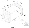
- the body has a first surface and a second surface opposing in the first direction, a third surface and a fourth surface connected to the first and second surfaces and opposing in a second direction, and a fifth surface and a sixth surface connected to the first to fourth surfaces and opposing in a third direction.
- the body includes a capacitance forming portion including the plurality of internal electrodes, and a cover portion disposed on both end surfaces of the capacitance forming portion in the first direction, and margin portions disposed on both end surfaces of the capacitance forming portion in the third direction.
- Gc is an average grain size of dielectric crystal grains included in the cover portion
- Ga is an average grain size of dielectric crystal grains included in the dielectric layer of the capacitance forming portion
- Gm is an average grain size of dielectric crystal grains included in the margin portion.
- the first direction may be defined as the stacking direction or thickness (T) direction
- the second direction may be defined as the length (L) direction
- the third direction may be defined as the width (W) direction.
- FIG. 1 schematically illustrates a perspective view of a multilayer electronic component according to an embodiment.
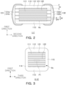
- FIG. 2 schematically illustrates a cross-sectional view taken along line I-I' of FIG. 1 .
- FIG. 3 schematically illustrates a cross-sectional view taken along line II-II' of FIG. 1 .
- FIG. 4 is a cross-sectional view taken along line II-II' of FIG. 1 to illustrate a measurement area of the present disclosure.
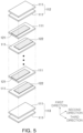
- FIG. 6 is an enlarged view of area P1 in FIG. 3 .
- FIG. 7 is an enlarged view of area P2 in FIG. 6 .
- FIG. 8 is an enlarged view of area P3 in FIG. 6 .
- a multilayer electronic component 100 according to an embodiment will be described in detail with reference to FIGS. 1 to 8 .
- a multilayer ceramic capacitor hereinafter referred to as 'MLCC'
- 'MLCC' multilayer ceramic capacitor
- the present disclosure is not limited thereto, and may also be applied to various multilayer electronic components using ceramic materials, such as inductors, piezoelectric elements, varistors, thermistors, or the like.
- the multilayer electronic component 100 includes a body 110 including a dielectric layer 111 and internal electrodes 121 and 122 alternately disposed with the dielectric layer 111 therebetween; and external electrodes 131 and 132 disposed on the body.
- a ratio of points at which a molar ratio of In/ (Ni+In) is 0.002 or more is 70% or more, and among central points in the first direction, a ratio of points at which a molar ratio of In/ (Ni+In) is 0.002 or more may be 35% or less.
- the ratio of points at which the molar ratio of In/(Ni+In) is 0.002 or more satisfies 70% or more, and the ratio of points with a molar ratio of In/(Ni+In) of 0.002 or more among the central points (•) in the first direction satisfies 35% or less. Therefore, breakage and clumping of internal electrodes may be suppressed and the reliability of multilayer electronic components may be improved.
- the body 110 may have a hexahedral shape or a similar shape. Due to shrinkage of the ceramic powder contained in the body 110 during the firing process, the body 110 may not have a hexahedral shape with completely straight lines, but may have a substantially hexahedral shape.
- the body 110 may have first and second surfaces 1 and 2 opposing in a first direction, third and fourth surfaces 3 and 4 connected to the first and second surfaces 1 and 2 and opposing in a second direction, and fifth and sixth surfaces 5 and 6 connected to the first and second surfaces 1 and 2, connected to the third and fourth surfaces 3 and 4, and opposing in a third direction.
- a corner connecting the first surface and the third to fifth surfaces and/or a corner connecting the second surface and the third to fifth surfaces may have a shape contracted toward the center of the body 110 in the first direction when viewed from the first or second surface.
- a corner connecting the first surface 1 and the third to sixth surfaces 3, 4, 5 and 6 and/or corners connecting the second surface 2 and the third to sixth surfaces 3, 4, 5 and 6 may have a shape contracted toward the center of the body 110 in the first direction when viewed from the first or second surface.
- the edges connecting respective surfaces of the body 110 are rounded by performing a separate process.
- the corner connecting the first surface and the third to sixth surfaces and/or the corner connecting the second surface and the third to sixth surfaces may have a round shape.
- the internal electrodes are cut to be exposed to the fifth and sixth surfaces 5 and 6 of the body, and then, when forming margin portions 114 and 115 by stacking a single dielectric layer or two or more dielectric layers on both sides of the capacitance forming portion Ac in the third direction (width direction), the portion connecting the first surface to the fifth and sixth surfaces and the portion connecting the second surface to the fifth and sixth surfaces may not have a contracted shape.
- the plurality of dielectric layers 111 forming the body 110 are in a sintered state, and the boundaries between adjacent dielectric layers 111 may be integrated to the extent that it is difficult to check without using a scanning electron microscope (SEM).
- SEM scanning electron microscope
- the number of stacked dielectric layers does not need to be particularly limited and may be determined considering the size of the multilayer electronic component.
- the body may be formed by stacking 400 or more dielectric layers.
- ceramic powder may be at least one of BaTiO 3 , (Ba 1-x Ca x )TiO 3 (0 ⁇ x ⁇ 1), Ba(Ti 1-y Ca y )O 3 (0 ⁇ y ⁇ 1), (Ba 1-x Ca x )(Ti 1-y Zr y )O 3 (0 ⁇ x ⁇ 1, 0 ⁇ y ⁇ 1) and Ba(Ti 1-y Zr y )O 3 (0 ⁇ y ⁇ 1).
- the dielectric layer 111 may include Ba(Ti 1-z In z )O 3 (0 ⁇ z ⁇ 1) .
- +3-valent In may be substituted at the Ti site of BaTiO 3 , the main component of the dielectric layer. When substituted at the Ti site, In may act as an acceptor and improve the reliability of multilayer electronic components.
- the main component of the dielectric layer 111 is at least one of BaTiO 3 , (Ba 1-x Ca x )TiO 3 (0 ⁇ x ⁇ 1), Ba(Ti 1-y Ca y )O 3 (0 ⁇ y ⁇ 1), (Ba 1-x Ca x )(Ti 1-y Zr y )O 3 (0 ⁇ x ⁇ 1, 0 ⁇ y ⁇ 1) and Ba(Ti 1-y Zr y )O 3 (0 ⁇ y ⁇ 1), and In diffuses into the dielectric layer 111 and replaces at the Ti site of a portion of the main components.
- Ba(Ti 1-2 In 2 )O 3 (0 ⁇ z ⁇ 1) may not be included as the main component.
- the dielectric layer 111 may include Sn. Additionally, the average content of Sn relative to Ti in the area of the dielectric layer 111 spaced 2 nm from the interface IF with the internal electrodes 121 and 122 may be 0.02 at% or more and 0.42 at% or less. Sn has a low melting point, and thus may play a role in allowing In to easily diffuse to the interface (IF) and may play a role in allowing In to be easily trapped at the interface (IF), thereby easily improving capacitance and high-temperature load lifespan.
- the above-described effect may be insufficient. If exceeding 0.42 at%, there is a risk that In diffusion may be excessive and the In content trapped at the interface may be reduced.
- the dielectric layer 111 may include Dy.
- Dy may play a role in improving high temperature load lifespan and dielectric constant.
- the average content of Dy relative to Ti in a region of the dielectric layer 111 2 nm away from the interface IF with the internal electrodes 121 and 122 may be 3 at% or more and 7 at% or less. Accordingly, the high-temperature load lifespan may be more easily improved and the dielectric constant may be improved.
- the dielectric layer 111 may further include various elements in addition to the elements described above.
- the dielectric layer 111 may further include at least one of Ca, Mn, V, Cr, Fe, Ni, Co, Cu, Zn, Mg, Si, and rare earth elements (RE).
- RE rare earth elements
- reliability may be prevented from being reduced even when the thickness of the plurality of dielectric layers 111 is relatively thin.
- the thickness of the dielectric layer is thick, reliability may be further improved. Therefore, there is no need to specifically limit an average thickness (td) of the dielectric layer 111, and the average thickness (td) of the dielectric layer 111 may be arbitrarily set depending on required characteristics or use.
- the average thickness (td) of the dielectric layer 111 may be 300 nm or more and 10 um or less.
- the average thickness (td) of at least one of the plurality of dielectric layers 111 may be 300 nm or more and 10 um or less.
- the average thickness (td) of the dielectric layer 111 may refer to the average size of the dielectric layer 111 disposed between the internal electrodes 121 and 122 in the first direction.
- the average thickness of the dielectric layer 111 may be measured by scanning cross-sections of the body 110 in the first and second directions with a scanning electron microscope (SEM) at a magnification of 10,000.
- the average value may be measured by measuring the thickness at multiple points of one dielectric layer 111, for example, 30 points at equal intervals in the second direction. The 30 equally spaced points may be designated in the capacitance forming portion Ac, which will be described later. Additionally, if this average value measurement is expanded to 10 dielectric layers 111 and the average value is measured, the average thickness of the dielectric layers 111 may be further generalized.
- the body 110 may include a capacitance forming portion (Ac), which is disposed inside the body 110 and in which capacitance is formed by including a first internal electrode 121 and a second internal electrode 122 disposed to face each other with the dielectric layer 111 interposed therebetween, and cover portions 112 and 113 formed above and below the capacitance forming portion Ac in the first direction.
- Ac capacitance forming portion
- the capacitance forming portion (Ac) is a part that contributes to forming the capacitance of the capacitor, and may be formed by repeatedly stacking a plurality of first and second internal electrodes 121 and 122 with the dielectric layer 111 interposed therebetween.
- the cover portions 112 and 113 may include an upper cover portion 112 disposed above the capacitance forming portion Ac in the first direction and a lower cover portion 113 disposed below the capacitance forming portion Ac in the first direction.
- the upper cover portion 112 and the lower cover portion 113 may be formed by stacking a single dielectric layer or two or more dielectric layers on the upper and lower surfaces of the capacitance forming portion Ac in the thickness direction, respectively, and basically, may play a role in preventing damage to the internal electrodes due to physical or chemical stress.
- the upper cover portion 112 and the lower cover portion 113 do not include internal electrodes and may include the same material as the dielectric layer 111.
- the upper cover portion 112 and the lower cover portion 113 may include a ceramic material, for example, a barium titanate (BaTiO 3 )-based ceramic material.
- a ceramic material for example, a barium titanate (BaTiO 3 )-based ceramic material.
- the thickness of the cover portions 112 and 113 does not need to be particularly limited.
- the thickness (tc) of the cover portions 112 and 113 may be 10 to 300 um.
- the thickness (tc) of the cover portions 112 and 113 may be 15 um or less.
- the average thickness (tc) of the cover portions 112 and 113 may refer to the size in the first direction, and may be an average value of sizes of the cover portions 112 and 113 in the first direction, measured at five points at equal intervals above or below the capacitance forming portion Ac.
- margin portions 114 and 115 may be disposed on the sides of the capacitance forming portion Ac.
- the margin portions 114 and 115 may include a first margin portion 114 disposed on the fifth surface 5 of the body 110 and a second margin portion 115 disposed on the sixth surface 6.
- the margin portions 114 and 115 may be disposed on both end surfaces of the ceramic body 110 in the width direction.
- the margin portions 114 and 115 may refer to the area between both ends of the first and second internal electrodes 121 and 122 and the boundary surface of the body 110 in a cross-section of the body 110 in the width-thickness (W-T) direction.
- the margin portions 114 and 115 may basically serve to prevent damage to the internal electrodes due to physical or chemical stress.
- the internal electrodes are cut to be exposed to the fifth and sixth surfaces 5 and 6 of the body, and then a single dielectric layer or two or more dielectric layers may be stacked on both sides of the capacitance forming portion Ac in the third direction (width direction) to form the margin portions 114 and 115.
- the width of the margin portions 114 and 115 does not need to be particularly limited.
- the width of the margin portions 114 and 115 may be 5 to 300 um.
- the average width of the margin portions 114 and 115 may be 15 um or less.
- the average width of the margin portions 114 and 115 may refer to the average size of the area in which the internal electrode is spaced apart from the fifth surface 5 in the third direction and the average size of the area in which the internal electrode is spaced apart from the sixth surface 6 in the third direction, and may be an average value of sizes of the margin portions 114 and 115 in the third direction, measured at five points at equal intervals on the side of the capacitance forming portion Ac.
- the average size of the areas where the internal electrodes 121 and 122 are spaced apart from the fifth and sixth surfaces 5 and 6 in the third direction may each be 15 um or less.
- the internal electrodes 121 and 122 may include first and second internal electrodes 121 and 122.
- the first and second internal electrodes 121 and 122 are alternately disposed to face each other with the dielectric layer 111 constituting the body 110 interposed therebetween, and may be exposed to the third and fourth surfaces 3 and 4 of the body 110, respectively.
- the ratio (A) of points at which the molar ratio of In/(Ni+In) is 0.002 or more may satisfy 70% or more
- the ratio (B) of points at which the molar ratio of In/(Ni+In) is 0.002 or more among the central points (•) in the first direction may satisfy 35% or less.
- the interfacial bonding force between the dielectric layer and the internal electrode may be improved, and the region with high In content may act as a kind of semiconductor barrier that prevents electron movement from the internal electrode to the dielectric layer or from the dielectric layer to the internal electrode. Therefore, both capacitance and high-temperature load lifespan may be improved.
- the molar ratio of In/ (Ni+In) may be calculated as [mol amount of In/(mol amount of Ni + mol amount of In)].
- the ratio of points at which the molar ratio of In/(Ni+In) is 0.002 or more is referred to as 'A'
- the ratio of points at which the molar ratio of In/(Ni+In) is 0.002 or more is referred to as 'B'.
- 'A' and 'B' may each be measured at at least 20 points.
- 'A' is greater than 0% but less than 70%, the capacitance may be improved compared to the case in which 'A' is 0%, but there is a risk that the high temperature load lifespan may be reduced. Therefore, 'A' may be, in detail, 70% or more, and to further improve capacitance and high temperature load lifespan, 'A' may be more preferably 75% or more. On the other hand, the upper limit of 'A' does not need to be particularly limited, and as a detailed example, 'A' may be 90% or less.
- 'B' exceeds 35%, there is a risk that the capacitance may decrease or the high-temperature load lifespan may decrease, and thus 'B' may be 35% or less.
- 'B' may be 20% or more.
- FIGS. 6 to 8 as an example of a method of measuring 'A' and 'B', after polishing the multilayer electronic component to the center in the second direction to expose the cross section in the first and third directions, in one internal electrode (121, 122), 20 points (A) spaced 10 nm apart from the interface (IF) with the dielectric layer 111 and 20 points (•) in the center in the first direction are selected, and at each of the selected points, the molar ratio of In/(Ni+In) may be measured through quantitative analysis of In and Ni by STEM-EDS, thereby obtaining 'A' and 'B'.
- the 20 points (A) spaced 10 nm apart from the interface (IF) with the dielectric layer 111 may be designated to have equal intervals.
- the 20 points (•) in the center in the first direction may also be designated to have equal intervals.
- the central portion of the internal electrode in the first direction may refer to the area located at the center when the internal electrode is divided into three parts in the first direction.
- the 20 points (•) in the center of the internal electrode in the first direction may be 20 random points selected from the center of the internal electrode of the first direction.
- an internal electrode is selected one by one in each of the central area located at the center of the body 100 in the width and thickness direction, the upper area adjacent to the upper cover portion 112, and the lower area adjacent to the lower cover portion 113, and after obtaining 'A' and 'B' from each internal electrode, an average value thereof may be calculated, and thus, the values of 'A' and 'B' may be more generalized.
- 'A' and 'B' may be controlled by controlling the amount of In compared to Ni added to the conductive paste and controlling the oxygen partial pressure conditions during firing.
- Indium (In) is an element with a stronger tendency to oxidize than nickel (Ni).
- Ni nickel
- a portion of In is oxidized and diffuses to the dielectric layer to replace Ti sites such as BaTiO 3 or the like, and the others are not oxidized and may form an alloy with Ni remaining in the internal electrode.
- a portion of the In that diffuses from the internal electrode toward the dielectric layer may be trapped at the interface between the dielectric layer and the internal electrode, forming a region with a high In content at the interface and the area adjacent to the interface.
- X-Y when the average value of the molar ratio of In/(Ni+In) at points 2 nm apart from the interface (IF) with the dielectric layer is X and the average value of the molar ratio of In/(Ni+In) at points 10 nm away from the interface (IF) with the dielectric layer is Y, X-Y may be 0.0041 or more.
- X-Y is greater than 0 and less than 0.0041, the capacitance decreases compared to when X-Y is 0, or there is a risk that high-temperature load lifespan may be reduced. Thus it may be difficult to improve both capacitance and high-temperature load lifespan. Therefore, in detail, X-Y may be 0.0041 or more, and to further improve capacitance and high temperature load lifespan, it may be more preferable for X-Y to be 0.0057 or more. On the other hand, there is no need to specifically limit the upper limit of X-Y, and as a preferred example, X-Y may be 0.0098 or less.
- the interface (IF) between the dielectric layer 111 and the internal electrodes 121 and 122 is observed by observing lines, for example, Fresnel fringes, which appear on both sides of the interface using a scanning transmission electron microscope (STEM).
- STEM scanning transmission electron microscope
- X may be less than or equal to 0.0139. If X is greater than 0.0139, the capacitance decreases or there is a risk that high-temperature load lifespan may be reduced, and thus it may be difficult to improve both capacitance and high-temperature load lifespan.
- X may be 0.0046 or more and 0.0139 or less, and Y may be 0.0005 or more and 0.0041 or less.
- X may be 0.0067 or more and 0.0139 or less, and Y may be 0.0010 or more and 0.0041 or less.
- the average grain size of the dielectric grains included in the cover portions 112 and 113 is Gc
- the average grain size of the dielectric grains included in the capacitance forming portion (Ac) is Ga
- the average grain size of the dielectric grains included in the margin portions 114 and 115 is Gm; 1 ⁇ Gc/Ga and 1 ⁇ Gm/Ga may be satisfied.
- the average grain size (Ga) of the dielectric grains included in the capacitance forming portion (Ac) may be controlled to be less than the average grain sizes (Gc, Gm) of the dielectric grains included in the cover portions 112 and 113 and the margin portions 114 and 115, thereby improving insulation resistance of the multilayer electronic component 100.
- the grain size of the dielectric grain may be determined by drawing a straight line from one point on the grain boundary of the dielectric grain to another point thereon, by referring the line with the greatest value as to the major axis and the line with the greatest value among the straight lines perpendicular to the major axis as to the minor axis, and by taking the average value of the major axis and the minor axis as the grain size of the dielectric crystal grain. Additionally, the average grain size of at least 100 dielectric crystal grains may be taken as the average grain size of the dielectric grains.
- the multilayer electronic component is polished to the center in the second direction to expose the first and third direction cross sections, and then, Ga, Gc, and Gm may be measured from an image obtained by scanning with a scanning electron microscope (SEM).
- SEM scanning electron microscope
- the magnification may vary depending on the grain size of the dielectric grains, and the magnification may be adjusted such that the grain size of at least 100 dielectric grains may be measured.
- FIG. 1 referring to FIG.
- Ga may be measured from an image scanned to include at least 100 dielectric crystal grains in a central area located in the center of the body 100 in the width and thickness directions
- Gc may be measured from an image scanned to include at least 100 dielectric crystal grains in the central area of the cover portion located in the center of the cover portions 112 and 113 in the width and thickness directions
- Gm may be measured from an image scanned to include at least 100 dielectric grains in the central area of the margin portion located in the center of the margin portions 114 and 115 in the width and thickness directions.
- the Ga and Gc may satisfy 1 ⁇ Gc/Ga ⁇ 1.28. If Gc/Ga is greater than 1.28, the average grain size (Ga) of the dielectric crystal grains included in the capacitance forming portion (Ac) is too small, and there is a risk that the capacitance may decrease and there is a risk that the variation in capacitance and/or Dissipation Factor (DF) may increase.
- Gc/Ga is greater than 1.28
- the average grain size (Ga) of the dielectric crystal grains included in the capacitance forming portion (Ac) is too small, and there is a risk that the capacitance may decrease and there is a risk that the variation in capacitance and/or Dissipation Factor (DF) may increase.
- the Ga and Gm may satisfy 1 ⁇ Gm/Ga ⁇ 1.07. If Gm/Ga is more than 1.07, the average grain size (Ga) of the dielectric crystal grains contained in the capacitance forming portion (Ac) is too small, and there is a risk that the capacitance may decrease and there is a risk that the variation in capacitance and/or Dissipation Factor (DF) may increase.
- Gm/Ga is more than 1.07
- the average grain size (Ga) of the dielectric crystal grains contained in the capacitance forming portion (Ac) is too small, and there is a risk that the capacitance may decrease and there is a risk that the variation in capacitance and/or Dissipation Factor (DF) may increase.
- DF Dissipation Factor
- the internal electrodes 121 and 122 include Ni and In, and at least a portion of In contained in the internal electrodes 121 and 122 may be present in an alloy form with Ni. Accordingly, the connectivity of the internal electrode is improved by reducing the grain boundary energy and surface tension of Ni, and the thickness deviation of the internal electrode may be reduced. Whether Ni and In are present in an alloy form may be confirmed by whether the peak position of Ni is shifted when analyzed by X-ray diffraction (XRD). For a detailed example, after pulverizing the internal electrode of a multilayer electronic component to obtain a powder form, the powder may be analyzed by XRD to determine whether the peak position of Ni has shifted.
- XRD X-ray diffraction
- the internal electrodes 121 and 122 may include Sn.
- Sn has a low melting point, and may thus play a role in allowing In to easily diffuse to the interface (IF). Sn may also serve to allow In to be easily trapped at the interface (IF), and thus serve to improve capacitance and high-temperature load lifespan more easily.
- the internal electrodes 121 and 122 may contain metals other than Ni, In, Ni-In, and Sn.
- the internal electrodes 121 and 122 may further include at least one of Cu, Pd, Ag, Au, Pt, Al, Ti, and alloys thereof.
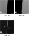
- FIG. 9A is an image of the interface between the internal electrode and the dielectric layer, analyzed by STEM-EDS, according to an embodiment, to show an image mapping the Ni element using STEM-EDS
- FIG. 9B is an image of the interface between the internal electrode and the dielectric layer, analyzed by STEM-EDS, according to an embodiment, to show an image mapping the Ti element using STEM-EDS
- FIG. 9C is an image of the interface between the internal electrode and the dielectric layer, analyzed by STEM-EDS, according to an embodiment, to show an image mapping the In element using STEM-EDS.
- the dielectric layer and the internal electrode may be clearly distinguished based on the Ni content and Ti content.
- FIG. 9C it can be seen that the In content is high at the interface between the dielectric layer and the internal electrode.
- FIG. 10A and FIG. 10B which is the result of a line profile using STEM-EDS along L1 illustrated in FIG. 9C , it can be seen that peak values of In, Dy, and Sn contents are detected within the area adjacent to the interface between the dielectric layer and the internal electrode.
- the peak value of In content is detected in the area in which the Ni content is more than 50 at% and 90 at% or less, which may be due to the diffusion of In contained in the conductive paste for internal electrodes into the dielectric layer. Therefore, in an embodiment, when analyzing the line profile of the area adjacent to the interface IF in a direction perpendicular to the interface between the dielectric layer and the internal electrode, the peak value of In content may be detected in the area in which the Ni content is more than 50 at% and 90 at% or less. In addition, the peak value of Sn content may also be detected in a region of more than 50 at% and 90 at% or less. At this time, line profile analysis may be performed using STEM-EDS.
- the peak value of Dy content is detected in the area in which the Ni content is 10 at% or more and less than 50 at%, which may be due to the diffusion of Dy added to the ceramic green sheet to the internal electrode. Therefore, in an embodiment, when analyzing the line profile of the area adjacent to the interface IF in a direction perpendicular to the interface between the dielectric layer and the internal electrode, the peak value of Dy content may be detected in an area in which the Ni content is 10 at% or more and less than 50 at%. At this time, line profile analysis may be performed using STEM-EDS.
- the internal electrodes 121 and 122 include ceramic particles, and the ceramic particles may include In.
- Ceramic particles included in the internal electrodes 121 and 122 may play a role in reducing the difference in sintering start temperature between the dielectric layer and the internal electrode. Ceramic particles added to the conductive paste for internal electrodes may be trapped within the internal electrode after firing. Additionally, as In is added to the conductive paste for internal electrodes, the ceramic particles included in the internal electrodes 121 and 122 may contain In.
- In may be mainly distributed on the surface of the ceramic particle, which is the interface between the ceramic particle and the internal electrode, similar to the interface (IF) between the internal electrode and the dielectric layer. Therefore, in the case of ceramic particles, the In content on the surface of ceramic particles is higher than the In content in the inside thereof, and the average content of In compared to Ti on the surface of the ceramic particle may be 0.3 at% or more. Additionally, the average content of In compared to Ti on the surface of the ceramic particle may be 0.3 at% or more and 3.8 at% or less.
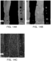
- FIG. 14A is an image of the interface between the internal electrode and the dielectric layer according to an embodiment, analyzed by STEM-EDS, to show an image mapping the Ni element using STEM-EDS
- FIG. 14B is an image of the interface between the internal electrode and the dielectric layer according to an embodiment, analyzed by STEM-EDS, to show an image mapping the Ti element using STEM-EDS
- FIG. 14C is an image of the interface between the internal electrode and the dielectric layer according to an embodiment, analyzed by STEM-EDS, to show an image mapping the In element using STEM-EDS.
- FIGS. 14A and 14B it can be seen that ceramic particles are trapped inside the internal electrode. Additionally, referring to FIG. 14C , it can be seen that the In content is high on the surface of the ceramic particles and it can be seen that the In content on the surface of the ceramic particle is similar to the In content at the interface (IF) between the internal electrode and the dielectric layer.
- the multilayer electronic component is polished to the center in the second direction to expose the cross section in the first and third directions, and then, five points at the boundary formed by one of the ceramic particles trapped in the internal electrodes 121 and 122 with the internal electrode are selected, and then, quantitative analysis of Ti and In by STEM-EDS is performed at the above five points to obtain the content of In compared to Ti, thereby calculating the average of values thereof and thus measuring the average content of In.
- four different ceramic particles may be selected among the trapped ceramic particles to measure five areas at each boundary between each ceramic particle and the internal electrode, thereby further generalizing by calculating the average value of a total of 20 measurements.
- the average thickness (te) of the internal electrodes 121 and 122 does not need to be particularly limited, and may be set arbitrarily depending on the required characteristics or use.
- the average thickness (te) of the internal electrodes 121 and 122 may be 300 nm or more and 3 um or less.
- the average thickness (te) of at least one of the plurality of internal electrodes 121 and 122 may be 300 nm or more and 3 um or less.
- the thickness of the internal electrodes 121 and 122 may refer to the size of the internal electrodes 121 and 122 in the first direction.
- the average thickness (te) of the internal electrode may be measured by scanning a cross-section of the body 110 in the first and second directions with a scanning electron microscope (SEM) at 10,000 magnification.
- the average value may be measured by measuring the thickness at multiple points of one internal electrode (121, 122), for example, at 30 points at equal intervals in the second direction. The 30 equally spaced points may be designated in the capacitance forming portion (Ac). Additionally, if this average value measurement is expanded to 10 internal electrodes 121 and 122 and the average value is measured, the average thickness of the internal electrodes 121 and 122 may be further generalized.
- ⁇ te/te when the average thickness of the internal electrodes 121 and 122 is te and the standard deviation of the thickness of the internal electrodes 121 and 122 is ⁇ te, ⁇ te/te may be 0.2 or less.
- the coefficient of variation (CV) of the thickness of the internal electrode may be 0.2 or less, which may indicate that the thickness uniformity of the internal electrode is within 20%.
- ⁇ te/te may be, in more detail, 0.18 or less, and more preferably 0.17 or less.
- the standard deviation ( ⁇ te) of the thickness of the internal electrodes 121 and 122 may be within ⁇ 70 nm.
- ⁇ te/te When ⁇ te/te is 0.2 or less, stress may be prevented from being unevenly applied to the internal electrodes 121 and 122 and electric field concentration may be prevented by ensuring uniformity of the thickness of the internal electrodes 121 and 122, thereby improving reliability.
- the standard deviation ( ⁇ te) of the thickness of the internal electrode may be measured by subtracting the average thickness (te) of the internal electrodes from each thickness measured at 30 equally spaced points in the second direction to then be squared, to measure the average thickness (te) of the internal electrodes 121 and 122, and by calculating the average of these values to obtain the variance, and then by taking the square root of the variance.
- the connectivity of the internal electrodes 121 and 122 may be 85% or more. Additionally, in more detail, the connectivity of the internal electrodes 121 and 122 may be 90% or more.
- the internal electrode (IE) includes a plurality of conductive portions (EP), and may include a disconnection portion (DP) between adjacent conductive portions (EP).
- EP conductive portions
- DP disconnection portion
- the connectivity of the internal electrodes may be measured from an image scanned of a cross-section of the body 110 in the first and second directions using a scanning electron microscope (SEM) at 10,000 magnification.
- SEM scanning electron microscope
- the average value thereof may be taken as the connectivity of the internal electrodes.
- the external electrodes 131 and 132 may be disposed on the third surface 3 and the fourth surface 4 of the body 110.
- the external electrodes 131 and 132 may include first and second external electrodes 131 and 132 respectively disposed on the third and fourth surfaces 3 and 4 of the body 110 and connected to the first and second internal electrodes 121 and 122, respectively.
- the number or shape of the external electrodes 131 and 132 may be changed depending on the shape of the internal electrodes 121 and 122 or other uses.
- the external electrodes 131 and 132 may be formed using any material as long as it has electrical conductivity, such as metal, and a detailed material of the external electrodes 131 and 132 may be determined considering electrical properties, structural stability, and the like, and may have a multilayer structure.
- the external electrodes 131 and 132 may include electrode layers 131a and 132a disposed on the body 110 and plating layers 131b and 132b formed on the electrode layers 131a and 132a.
- the electrode layers 131a and 132a are firing electrodes containing conductive metal and glass, or may be a resin-based electrode containing a conductive metal and resin.
- the electrode layers 131a and 132a may be formed by sequentially forming a firing electrode and a resin-based electrode on a body. Additionally, the electrode layers 131a and 132a may be formed by transferring a sheet containing conductive metal onto the body, or may be formed by transferring a sheet containing conductive metal onto a firing electrode. Additionally, the electrode layers 131a and 132a may be formed as a plating layer or may be a layer formed using a deposition method such as sputtering or Atomic layer deposition (ALD).
- ALD Atomic layer deposition
- the conductive metal included in the electrode layers 131a and 132a a material with excellent electrical conductivity may be used and is not particularly limited.
- the conductive metal may be at least one of nickel (Ni), copper (Cu), and an alloy thereof.
- the plating layers 131b and 132b serve to improve mounting characteristics.
- the types of plating layers 131b and 132b are not particularly limited, and may be a plating layer containing at least one of Ni, Sn, Pd, and alloys thereof, and may be formed of multiple layers.
- the plating layers 131b and 132b may be Ni plating layers or Sn plating layers, and may be in the form in which a Ni plating layer and a Sn plating layer are formed sequentially on the electrode layers 131a and 132a, and may be in the form in which the Sn plating layer, Ni plating layer, and Sn plating layer are formed sequentially. Additionally, the plating layers 131b and 132b may include a plurality of Ni plating layers and/or a plurality of Sn plating layers. Additionally, the plating layers 131b and 132b may be formed by sequentially forming a Ni plating layer and a Pd plating layer on the electrode layers 131a and 132a.
- the size of the multilayer electronic component 100 does not need to be particularly limited.
- the multilayer electronic component 100 according to an embodiment of the present disclosure may be advantageous for miniaturization and high capacitance, and may thus be applied to small IT products. Because high reliability may be secured in a variety of environments, the multilayer electronic component 100 according to an embodiment may also be applied to the size of automotive electronic products that require high reliability.
- Ceramic green sheets coated with internal electrode paste were stacked and cut and fired to form a body. Then, a sample chip was produced by applying paste for external electrodes on the body and firing the same.
- sample chips were manufactured by varying the In content compared to the Ni powder contained in the internal electrode paste for respective test numbers.
- In test number 1 In was not added to the paste for internal electrodes.
- the ceramic green sheet was manufactured by adding an organic solvent, a binder, and dispersant to barium titanate (BaTiO 3 ) powder. In was not added to the ceramic green sheet.
- the thinned sample was processed to have a thickness of 60 nm or less.
- the damage layer on the sample surface formed during FIB processing was removed by Ar ion milling.
- An internal electrode was selected one by one from each of the thinned samples produced as described above, and was analyzed using a scanning transmission electron microscope (STEM) and an energy dispersive X-ray analysis device (EDS).
- STEM scanning transmission electron microscope
- EDS energy dispersive X-ray analysis device
- an ARM-200F JEOL product
- the acceleration voltage was 200kV.
- oxford EDS was used as the EDS equipment.
- 'A' which is the ratio of points at which the molar ratio of In/(Ni+In) is 0.002 or more
- 'B' which is the ratio of points at which the molar ratio of In/(Ni+In) is 0.002 or more among the central points of the internal electrode in the first direction
- X which is the average value of the molar ratio of In/(Ni+In) at points (x) 2 nm apart from the interface (IF) with the dielectric layer
- Y which is the average value of the molar ratio of In/(Ni+In) at points 10 nm apart from the interface (IF) with the dielectric layer
- the measurement probe diameter of the electron beam was set to about 1 nm, and the measurement time was set to 30 seconds.
- quantitative correction from the obtained EDS spectrum used Cliff-Lorimer correction.
- Capacitance was measured on 10 sample chips for each test number, and by using an automatic bridge measuring device, the capacitance was measured under the conditions of AC voltage of 1Vrms and 1kHz, and the average value for each test number was obtained.
- the capacitance of test number 1 was set as the standard value '1', and test numbers 2 to 9 were recorded as relative values to the capacitance of test number 1.
- MTTF Mean Time to Failure
- test numbers 3 to 6 in cases in which X-Y satisfies 0.0041 or more (test numbers 3 to 6) it can be seen that there is a significant improvement in both capacitance and MTTF compared to test number 1.
- the connectivity of the internal electrode is 85% or more, and the thickness deviation ( ⁇ te/te) of the internal electrode is also small, 0.20 or less.
- ⁇ te/te thickness deviation
- Comparative Example 1 corresponds to test number 1 in Experimental Example 1, and the inventive example corresponds to test number 4 in Experimental Example 1.
- Comparative Example 2 a sample chip was manufactured by adding Sn to the internal electrode paste without adding In, in which the In content compared to the Ni powder contained in the internal electrode paste of Test No. 4 and the Sn content compared to the Ni powder contained in the internal electrode paste of Comparative Example 2 were made to be the same.
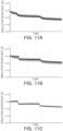
- FIG. 11A is a graph for measurement of the insulation resistance for Comparative Example 1
- FIG. 11B is a graph for Comparative Example 2
- FIG. 11C is a graph for the inventive example.
- FIGS. 11A, 11B and 11C it can be seen that in the case of Comparative Example 2 in which Sn was added, the insulation resistance is improved compared to Comparative Example 1, but the distribution of the insulation resistance is not improved. Meanwhile, in the case of the inventive example, it can be seen that not only the insulation resistance is improved compared to Comparative Examples 1 and 2, but also the distribution of the insulation resistance is significantly improved.
- the spread (CV value) of the insulation resistance of Comparative Example 1 was measured to be 15%
- the spread (CV value) of the insulation resistance of Comparative Example 2 was measured to be 18%
- the spread (CV value) of the insulation resistance of the Inventive example was measured to be 7%.
- each sample chip was polished to the center in the second direction to expose the cross section in the first and third directions and then observed using a scanning electron microscope (SEM).
- SEM scanning electron microscope
- Capacitance and Dissipation Factor (DF) were measured, and the average and CV values are listed in Table 3 below.
- Capacitance and Dissipation Factor (DF) were measured using an automatic bridge-type measuring device under the conditions of AC voltage of 1Vrms and 1kHz.
- capacitance of Comparative Example 1 was set as the standard value '1', and in the case of the inventive example, the relative value to the capacitance of Comparative Example 1 was provided.
- the capacitance of the inventive example to which In was added is higher than the capacitance of Comparative Example 1, and in detail, it can be seen that the capacitance CV value is significantly improved.
- the DF of the inventive example is slightly higher than DF of Comparative Example 1, the DF CV value is significantly lower.
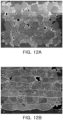
- FIGS. 12A to 13B images of dielectric grains scanned by SEM are illustrated in FIGS. 12A to 13B .
- FIG. 12A is an image observing the dielectric crystal grains of the cover portion of Comparative Example 1
- FIG. 12B is an image observing dielectric crystal grains in the capacitance forming portion of Comparative Example 1.
- FIG. 13A is an image observing the dielectric crystal grains of the cover portion of the inventive example
- FIG. 13B is an image observing dielectric crystal grains in the capacitance forming portion of the inventive example.
- the average grain size (Ga) of the dielectric grains included in the capacitance forming portion is very small compared to the average grain size (Gc) of the dielectric grains included in the cover portion and the average grain size (Gm) of the dielectric grains included in the margin portion.
- the average grain size (Ga) of the dielectric grains included in the capacitance forming portion is similar to the average grain size (Gc) of the dielectric grains included in the cover portion and the average grain size (Gm) of the dielectric grains included in the margin portion.
- reliability of multilayer electronic components may be improved by controlling the In content in each position within the internal electrode.
- Capacitance and high-temperature load lifespan of multilayer electronic components may be improved.
- Connectivity of the internal electrodes may be improved and a thickness deviation of the internal electrodes may be reduced.
- Dispersion of insulation resistance may be suppressed.
Landscapes
- Engineering & Computer Science (AREA)
- Power Engineering (AREA)
- Manufacturing & Machinery (AREA)
- Microelectronics & Electronic Packaging (AREA)
- Chemical & Material Sciences (AREA)
- Ceramic Engineering (AREA)
- Materials Engineering (AREA)
- Inorganic Chemistry (AREA)
- Fixed Capacitors And Capacitor Manufacturing Machines (AREA)
- Ceramic Capacitors (AREA)
Applications Claiming Priority (2)
| Application Number | Priority Date | Filing Date | Title |
|---|---|---|---|
| KR20230008272 | 2023-01-19 | ||
| KR1020230015116A KR20240115683A (ko) | 2023-01-19 | 2023-02-03 | 적층형 전자 부품 |
Publications (2)
| Publication Number | Publication Date |
|---|---|
| EP4404222A2 true EP4404222A2 (de) | 2024-07-24 |
| EP4404222A3 EP4404222A3 (de) | 2025-01-15 |
Family
ID=89573904
Family Applications (1)
| Application Number | Title | Priority Date | Filing Date |
|---|---|---|---|
| EP24151136.9A Pending EP4404222A3 (de) | 2023-01-19 | 2024-01-10 | Mehrschichtiges keramisches elektronisches bauelement, das in seinem mittleren teil ein molverhältnis von in/(ni+in) von 0,002 oder mehr aufweist, das 70 % oder mehr beträgt |
Country Status (3)
| Country | Link |
|---|---|
| US (1) | US20240249886A1 (de) |
| EP (1) | EP4404222A3 (de) |
| JP (1) | JP2024102824A (de) |
Family Cites Families (6)
| Publication number | Priority date | Publication date | Assignee | Title |
|---|---|---|---|---|
| CN105793938B (zh) * | 2013-12-10 | 2019-04-12 | 株式会社村田制作所 | 层叠陶瓷电容器以及层叠陶瓷电容器的制造方法 |
| KR102442835B1 (ko) * | 2018-03-28 | 2022-09-14 | 삼성전기주식회사 | 적층형 커패시터 |
| KR102355658B1 (ko) * | 2018-08-16 | 2022-01-26 | 삼성전기주식회사 | 적층 세라믹 전자부품 |
| KR20220131609A (ko) * | 2021-03-22 | 2022-09-29 | 삼성전기주식회사 | 적층 세라믹 전자부품 |
| US11967462B2 (en) * | 2021-06-30 | 2024-04-23 | Samsung Electro-Mechanics Co., Ltd. | Capacitor component including indium and tin, and method of manufacturing the capacitor component |
| KR20230099932A (ko) * | 2021-12-28 | 2023-07-05 | 삼성전기주식회사 | 적층형 전자 부품 |
-
2023
- 2023-12-22 US US18/394,032 patent/US20240249886A1/en active Pending
- 2023-12-27 JP JP2023221251A patent/JP2024102824A/ja active Pending
-
2024
- 2024-01-10 EP EP24151136.9A patent/EP4404222A3/de active Pending
Also Published As
| Publication number | Publication date |
|---|---|
| JP2024102824A (ja) | 2024-07-31 |
| US20240249886A1 (en) | 2024-07-25 |
| EP4404222A3 (de) | 2025-01-15 |
Similar Documents
| Publication | Publication Date | Title |
|---|---|---|
| CN114649146A (zh) | 介电晶粒和陶瓷电子组件 | |
| CN116013688A (zh) | 陶瓷电子组件 | |
| JP7813394B2 (ja) | 積層型電子部品及びその製造方法 | |
| KR102900300B1 (ko) | 적층형 전자 부품 | |
| CN114613597A (zh) | 介电组合物和包括该介电组合物的多层电子组件 | |
| EP4401100A2 (de) | Mehrschichtiges elektronisches bauteil | |
| EP4404222A2 (de) | Mehrschichtiges keramisches elektronisches bauelement, das in seinem mittleren teil ein molverhältnis von in/(ni+in) von 0,002 oder mehr aufweist, das 70 % oder mehr beträgt | |
| US12278057B2 (en) | Ceramic electronic component including barium calcium titanate | |
| CN116364419A (zh) | 介电组合物和多层电容器 | |
| EP4365150A2 (de) | Mehrschichtiges elektronische keramische bauteil | |
| US20260045412A1 (en) | Multilayer electronic component | |
| US12400790B2 (en) | Multilayer electronic component | |
| EP4451300A2 (de) | Mehrschichtiges elektronisches bauteil | |
| KR20240115683A (ko) | 적층형 전자 부품 | |
| US20250218677A1 (en) | Multilayer electronic component | |
| US20260038740A1 (en) | Multilayer electronic component | |
| KR20240064490A (ko) | 적층형 전자 부품 | |
| CN118366788A (zh) | 多层电子组件 | |
| KR20250027168A (ko) | 적층형 전자 부품 | |
| CN116469686A (zh) | 多层电子组件 | |
| CN117995553A (zh) | 多层电子组件 | |
| CN114628153A (zh) | 多层电子组件 | |
| JP2025098965A (ja) | 積層型電子部品 | |
| KR20250096501A (ko) | 적층형 전자 부품 | |
| JP2024095927A (ja) | 積層型電子部品 |
Legal Events
| Date | Code | Title | Description |
|---|---|---|---|
| PUAI | Public reference made under article 153(3) epc to a published international application that has entered the european phase |
Free format text: ORIGINAL CODE: 0009012 |
|
| STAA | Information on the status of an ep patent application or granted ep patent |
Free format text: STATUS: REQUEST FOR EXAMINATION WAS MADE |
|
| 17P | Request for examination filed |
Effective date: 20240110 |
|
| AK | Designated contracting states |
Kind code of ref document: A2 Designated state(s): AL AT BE BG CH CY CZ DE DK EE ES FI FR GB GR HR HU IE IS IT LI LT LU LV MC ME MK MT NL NO PL PT RO RS SE SI SK SM TR |
|
| PUAL | Search report despatched |
Free format text: ORIGINAL CODE: 0009013 |
|
| AK | Designated contracting states |
Kind code of ref document: A3 Designated state(s): AL AT BE BG CH CY CZ DE DK EE ES FI FR GB GR HR HU IE IS IT LI LT LU LV MC ME MK MT NL NO PL PT RO RS SE SI SK SM TR |
|
| RIC1 | Information provided on ipc code assigned before grant |
Ipc: H01G 4/012 20060101ALI20241209BHEP Ipc: H01G 4/008 20060101ALI20241209BHEP Ipc: H01G 4/30 20060101ALI20241209BHEP Ipc: H01G 4/12 20060101ALI20241209BHEP Ipc: H01G 4/00 20060101AFI20241209BHEP |