EP4404098A1 - Automatischer layoutroutingfluss zur beurteilung des verpackungssubstratdesigns - Google Patents
Automatischer layoutroutingfluss zur beurteilung des verpackungssubstratdesigns Download PDFInfo
- Publication number
- EP4404098A1 EP4404098A1 EP24150554.4A EP24150554A EP4404098A1 EP 4404098 A1 EP4404098 A1 EP 4404098A1 EP 24150554 A EP24150554 A EP 24150554A EP 4404098 A1 EP4404098 A1 EP 4404098A1
- Authority
- EP
- European Patent Office
- Prior art keywords
- routing
- groups
- features
- point
- swapping
- Prior art date
- Legal status (The legal status is an assumption and is not a legal conclusion. Google has not performed a legal analysis and makes no representation as to the accuracy of the status listed.)
- Pending
Links
Images




Classifications
-
- G—PHYSICS
- G06—COMPUTING OR CALCULATING; COUNTING
- G06F—ELECTRIC DIGITAL DATA PROCESSING
- G06F30/00—Computer-aided design [CAD]
- G06F30/30—Circuit design
- G06F30/39—Circuit design at the physical level
- G06F30/394—Routing
-
- G—PHYSICS
- G06—COMPUTING OR CALCULATING; COUNTING
- G06F—ELECTRIC DIGITAL DATA PROCESSING
- G06F30/00—Computer-aided design [CAD]
- G06F30/20—Design optimisation, verification or simulation
- G06F30/27—Design optimisation, verification or simulation using machine learning, e.g. artificial intelligence, neural networks, support vector machines [SVM] or training a model
-
- G—PHYSICS
- G06—COMPUTING OR CALCULATING; COUNTING
- G06F—ELECTRIC DIGITAL DATA PROCESSING
- G06F30/00—Computer-aided design [CAD]
- G06F30/30—Circuit design
- G06F30/39—Circuit design at the physical level
- G06F30/392—Floor-planning or layout, e.g. partitioning or placement
-
- G—PHYSICS
- G06—COMPUTING OR CALCULATING; COUNTING
- G06F—ELECTRIC DIGITAL DATA PROCESSING
- G06F2119/00—Details relating to the type or aim of the analysis or the optimisation
- G06F2119/02—Reliability analysis or reliability optimisation; Failure analysis, e.g. worst case scenario performance, failure mode and effects analysis [FMEA]
-
- G—PHYSICS
- G06—COMPUTING OR CALCULATING; COUNTING
- G06F—ELECTRIC DIGITAL DATA PROCESSING
- G06F30/00—Computer-aided design [CAD]
- G06F30/30—Circuit design
- G06F30/39—Circuit design at the physical level
- G06F30/398—Design verification or optimisation, e.g. using design rule check [DRC], layout versus schematics [LVS] or finite element methods [FEM]
Definitions
- the invention relates to layout routing, and in particular, to a method of auto-routing.
- the prior art layout uses manual routing.
- AI artificial intelligence
- HPC High Performance Computing
- a layout routing method includes determining a routing pattern according to a swapping rule, a via pattern, area constraints and pin locations; optimizing swapping in differential pairs according to the routing pattern; extracting features of each routing net to obtain extracted features; using an unsupervised algorithm to generate different routing groups according to the extracted features; and determining a routing order of the routing groups according to complex features of the routing groups.
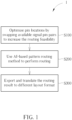
- FIG. 1 is a flowchart of an integrated auto layout routing method 1 according to an embodiment of the present invention.
- the integrated auto layout routing method 1 can save human effort on routing and layout evaluation by optimizing pin allocation and using AI (artificial intelligence) -based pattern routing method to perform routing.
- the integrated auto layout routing method 1 comprises Steps S100 to S300. Any reasonable step change or adjustment is within the scope of the disclosure. Steps S100 to S300 are explained as follows: Step S100: Optimize pin locations by swapping available signal pin pairs to increase the routing feasibility; Step S200: use AI-based pattern routing method to perform routing; Step S300: export and translate the routing result to different layout format.
- Step S100 calculate the cost of every layer before and after swapping to determine whether to swap the pin locations or not, and then swap differential pairs according to the cost.
- the cost can be determined according to the cross angle degree of every two fly-lines and the number of cross fly-lines. Fly-lines are virtual connections between pins which provide a rough idea of all the traces that will have to be created to complete those connections.
- Step S200 apply an AI-based pattern routing method, which optimizes swapping in differential pairs according to the determined routing pattern and then use unsupervised clustering algorithms to generate different routing groups according to the features extracted from the routing nets.
- After generating different routing groups determine a routing order according to complexity of the routing groups and perform routing in sequence. The more complex the group, the earlier the routing will be performed. By using this method, the appearances of detours can be reduced and the routing path distance can be reduced. If the routing fails, perform the rip-up rerouting algorithm to fix the fail net.
- Step S300 the routing result can be exported and translated to different layout format for user to input.
- FIG. 2 is a flowchart of Step S100; Step S100 applies a Heuristic-based pin location swap algorithm. Step S100 is performed before Step S200 in order to improve the layout routing feasibility by optimizing pin allocation. Step S100 improves routing feasibility for routers by calculating cost of allocation and swap the pin pairs.
- S100 may include Steps S101 to S103. Any reasonable step change or adjustment is within the scope of the disclosure. Steps S101 to S103 are explained as follows: Step S101: Calculate every two fly-lines' cross angle degree; Step S102: calculate the cost of every layer to determine whether to swap or not; Step S103: optimize pin allocation by swapping differential pairs.
- Step S102 calculate the cost of every layer.
- the cost is determined according to the cross angle degree of every two fly-lines and the number of cross fly-lines. If two fly-lines cross, which indicates the routing path would be longer, the cost will be higher; if two fly-lines are in parallel, the cost will be lower.
- Step S103 calculate the midpoints of every differential pair's bump-out and ball location to get the approximate routing direction, and then determine the differential pair locations and swap differential pairs according to the cost.
- FIG. 3 shows a result after performing Step S100 of the method 1. It shows the result by layer.
- L2, L4, L6 represents layer 2, layer 4, layer 6 respectively.
- the cross number indicates the number of the cross fly-lines and the percentage indicates the percentage of cross fly-lines decrease after performing pin swaps. For example, -41.1% in FIG. 3 indicates the number of the cross fly-lines in layer 2 has been reduced by 41.1% compared to the original and the number of the cross fly-lines in layer 2 is 303.
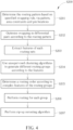
- FIG. 4 is a flowchart of Step S200 of using AI-based pattern routing method.
- Step S200 performs routing based on available router in commercial EDA (electronic design automation) layout tools, and it can help to find the feasible path of routing and save human resource.
- Step S200 can be used with different routing algorithm, and may include Steps S201 to S207. Any reasonable step change or adjustment is within the scope of the disclosure.
- Steps S201 to S207 are explained as follows: Step S201: Determine the routing pattern based on specified swapping rule, via pattern, area constraints and pin locations; Step S202: optimize swapping in differential pairs according to the routing pattern; Step S203: extract features of each routing net; Step S204: use unsupervised clustering algorithms to generate different routing groups according to the features; Step S205: determine a routing order according to complex features of the routing groups; Step S206: perform routing for each group; Step S207: perform rip-up rerouting algorithm.
- Step S201 the via pattern shows the locations and traces of vias which are electrical connections between layers.
- the pin locations are locations of the bump-outs and ball pins.
- the features comprise start point Vs, target point Vt, breakout point Vb, vector (Vs, Vt), vector (Vs, Vb), vector (Vt, Vb), Manhattan distance between breakout point Vb and target point Vt, which is a sum of a distance between x coordinates of the breakout point Vb and target point Vt and a distance between y coordinates of the breakout point Vb and target point Vt, and vectors (Vt, Vb) of adjacent nets.
- the unsupervised clustering algorithms can be K-means or Mean Shift.
- Step S205 is performed after generating different routing groups.
- the complex features of the routing groups comprise the number of nets, the number of fanout crossing points, and the total fanout trace length. Fanouts are traces from a device lands to adjacent via.
- Step S206 route each group in the order determined in Step S205.
- Step S207 perform the rip-up rerouting algorithm when routing fails.
- the router can fail by not connecting terminals that should be connected or by mistakenly connecting two terminals that should not be connected.
- the rip-up rerouting algorithm comprises reducing boundary errors of clustering by using a convex hull, swapping pins in failed differential pairs to generate a different layout pattern and dividing the failed routing group into two sub-groups by a failed routing net. After dividing the failed routing group into two sub-groups, reroute the sub-groups.
- FIG. 5 shows a result after performing clustering and determining the routing order in FIG. 4 .
- the left side of FIG. 5 shows a result of manual grouping and the right side of FIG. 5 shows a result after clustering and routing in the determined order.
- FIG. 6 shows taking the failed net as a boundary for dividing the original group into two sub-groups.
- the left side of FIG. 6 shows a result of the original group with a failed net, the failed net in FIG. 6 has no routing resources.
- the right side of FIG. 6 shows a result of rerouting the sub-groups. After dividing the original group into sub-groups, reroute the sub-groups and the failed net is fixed.
- Step S300 After finishing the routing, perform Step S300 to export the routing result. Since the format of the routing may be different from the format of the layout, in Step S300, it can translate the routing result to a different layout format and export the translated routing result for user to input.
- FIG. 7 shows a computer system for performing an integrated auto layout routing method.
- the computer system 7 includes a central processing unit (CPU) 71, a display device 73, an input device 74, and a non-transitory computer-readable medium 75.
- the display device 73, the input device 74 and the non-transitory computer-readable medium 75 are connected to the central processing unit (CPU) 71.
- the non-transitory computer-readable medium 75 storing computer-executable instructions thereon, that when executed by the central processing unit (CPU) 71, cause the central processing unit (CPU) 71 to perform the integrated auto layout routing method 1 and the routing result may be displayed on a graphical user interface (GUI) 72 on the display device 73. Users may interact with the graphical user interface 72 and interact with the routing result using the input device 74.
- the input device 74 can be a mouse, a touch pad or a keyboard.
Landscapes
- Engineering & Computer Science (AREA)
- Theoretical Computer Science (AREA)
- Physics & Mathematics (AREA)
- Computer Hardware Design (AREA)
- Evolutionary Computation (AREA)
- General Engineering & Computer Science (AREA)
- Geometry (AREA)
- General Physics & Mathematics (AREA)
- Computer Networks & Wireless Communication (AREA)
- Architecture (AREA)
- Artificial Intelligence (AREA)
- Computer Vision & Pattern Recognition (AREA)
- Medical Informatics (AREA)
- Software Systems (AREA)
- Design And Manufacture Of Integrated Circuits (AREA)
Applications Claiming Priority (2)
| Application Number | Priority Date | Filing Date | Title |
|---|---|---|---|
| US202363480316P | 2023-01-18 | 2023-01-18 | |
| US18/395,633 US20240242016A1 (en) | 2023-01-18 | 2023-12-25 | Automatic layout routing flow for package substrate design evaluation |
Publications (1)
| Publication Number | Publication Date |
|---|---|
| EP4404098A1 true EP4404098A1 (de) | 2024-07-24 |
Family
ID=89474554
Family Applications (1)
| Application Number | Title | Priority Date | Filing Date |
|---|---|---|---|
| EP24150554.4A Pending EP4404098A1 (de) | 2023-01-18 | 2024-01-05 | Automatischer layoutroutingfluss zur beurteilung des verpackungssubstratdesigns |
Country Status (3)
| Country | Link |
|---|---|
| US (1) | US20240242016A1 (de) |
| EP (1) | EP4404098A1 (de) |
| TW (1) | TW202431138A (de) |
Citations (3)
| Publication number | Priority date | Publication date | Assignee | Title |
|---|---|---|---|---|
| US5757656A (en) * | 1995-12-20 | 1998-05-26 | Mentor Graphics | Method for routing breakouts |
| US10755026B1 (en) * | 2017-11-14 | 2020-08-25 | Synopsys, Inc. | Circuit design including design rule violation correction utilizing patches based on deep reinforcement learning |
| US20220405458A1 (en) * | 2021-06-16 | 2022-12-22 | Synopsys, Inc. | Machine-learning-based power/ground (p/g) via removal |
-
2023
- 2023-12-25 US US18/395,633 patent/US20240242016A1/en active Pending
-
2024
- 2024-01-05 EP EP24150554.4A patent/EP4404098A1/de active Pending
- 2024-01-12 TW TW113101310A patent/TW202431138A/zh unknown
Patent Citations (3)
| Publication number | Priority date | Publication date | Assignee | Title |
|---|---|---|---|---|
| US5757656A (en) * | 1995-12-20 | 1998-05-26 | Mentor Graphics | Method for routing breakouts |
| US10755026B1 (en) * | 2017-11-14 | 2020-08-25 | Synopsys, Inc. | Circuit design including design rule violation correction utilizing patches based on deep reinforcement learning |
| US20220405458A1 (en) * | 2021-06-16 | 2022-12-22 | Synopsys, Inc. | Machine-learning-based power/ground (p/g) via removal |
Non-Patent Citations (2)
| Title |
|---|
| ANONYMOUS: "Optimum Design Associates - Printed Ciruit Board Design and Assembly - Designer's Handbook", 1 March 2016 (2016-03-01), XP055639800, Retrieved from the Internet <URL:http://optimumcontent.org/wp-content/uploads/2016/03/Optimum-Design-Handbook.pdf> [retrieved on 20191107] * |
| YIBO LIN: "Asynchronous Reinforcement Learning Framework and Knowledge Transfer for Net-Order Exploration in Detailed Routing", vol. 41, no. 9, 22 August 2022 (2022-08-22), USA, pages 3132 - 3142, XP093154766, ISSN: 0278-0070, Retrieved from the Internet <URL:https://ieeexplore.ieee.org/stampPDF/getPDF.jsp?tp=&arnumber=9557780&ref=aHR0cHM6Ly9pZWVleHBsb3JlLmllZWUub3JnL2RvY3VtZW50Lzk1NTc3ODA=> DOI: 10.1109/TCAD.2021.3117505 * |
Also Published As
| Publication number | Publication date |
|---|---|
| TW202431138A (zh) | 2024-08-01 |
| US20240242016A1 (en) | 2024-07-18 |
Similar Documents
| Publication | Publication Date | Title |
|---|---|---|
| Hsu et al. | NTUplace4h: A novel routability-driven placement algorithm for hierarchical mixed-size circuit designs | |
| CN101482893B (zh) | 半导体装置制造方法 | |
| US11176306B2 (en) | Methods and systems to perform automated Integrated Fan-Out wafer level package routing | |
| CN103198177A (zh) | 基于gpu的集成电路电容参数提取系统及方法 | |
| CN108959693B (zh) | 设计集成电路的方法,以及制造集成电路的方法 | |
| CN102637217B (zh) | 基于云计算平台的大规模集成电路布线系统 | |
| CN107436965A (zh) | 设计集成电路的计算机实现的方法 | |
| US10346579B2 (en) | Interactive routing of connections in circuit using auto welding and auto cloning | |
| US11861286B2 (en) | Segregating defects based on computer-aided design (CAD) identifiers associated with the defects | |
| US20240386183A1 (en) | Through-silicon vias in integrated circuit packaging | |
| US8850374B2 (en) | Method of reducing parasitic mismatch | |
| Farooq et al. | Exploring and optimizing partitioning of large designs for multi-FPGA based prototyping platforms | |
| CN110147139B (zh) | 计算机执行方法、时脉数据处理系统以及计算机可读取储存媒体 | |
| Taniguchi et al. | Two-layer bottleneck channel track assignment for analog VLSI | |
| US20240242016A1 (en) | Automatic layout routing flow for package substrate design evaluation | |
| US20200394352A1 (en) | Satisfiability sweeping for synthesis | |
| US8621411B1 (en) | Generating and selecting bit-stack candidates from a graph using dynamic programming | |
| CN112214956B (zh) | 用于设计半导体电路的系统及其操作方法 | |
| US11023645B1 (en) | Method, system, and product to efficiently route interconnections following a free form contour | |
| Huang et al. | Deep learning based refinement for package substrate routing | |
| US20180046744A1 (en) | Systems and methods for cell abutment | |
| CN112560386A (zh) | 一种大规模复杂版图电阻提取加速方法 | |
| US20230061120A1 (en) | Routing of high-speed, high-throughput interconnects in integrated circuits | |
| CN113515915B (zh) | 插入填充单元的方法、装置、设备以及存储介质 | |
| CN118364776A (zh) | 布局布线方法及非暂时性计算机可读取媒体 |
Legal Events
| Date | Code | Title | Description |
|---|---|---|---|
| PUAI | Public reference made under article 153(3) epc to a published international application that has entered the european phase |
Free format text: ORIGINAL CODE: 0009012 |
|
| STAA | Information on the status of an ep patent application or granted ep patent |
Free format text: STATUS: THE APPLICATION HAS BEEN PUBLISHED |
|
| AK | Designated contracting states |
Kind code of ref document: A1 Designated state(s): AL AT BE BG CH CY CZ DE DK EE ES FI FR GB GR HR HU IE IS IT LI LT LU LV MC ME MK MT NL NO PL PT RO RS SE SI SK SM TR |
|
| STAA | Information on the status of an ep patent application or granted ep patent |
Free format text: STATUS: REQUEST FOR EXAMINATION WAS MADE |
|
| 17P | Request for examination filed |
Effective date: 20250120 |
|
| STAA | Information on the status of an ep patent application or granted ep patent |
Free format text: STATUS: EXAMINATION IS IN PROGRESS |
|
| 17Q | First examination report despatched |
Effective date: 20250314 |