EP4403901A1 - Zweistufiges verfahren zur herstellung von plasmonischen nanostrukturen für plasmonisches biosensing - Google Patents
Zweistufiges verfahren zur herstellung von plasmonischen nanostrukturen für plasmonisches biosensing Download PDFInfo
- Publication number
- EP4403901A1 EP4403901A1 EP23382034.9A EP23382034A EP4403901A1 EP 4403901 A1 EP4403901 A1 EP 4403901A1 EP 23382034 A EP23382034 A EP 23382034A EP 4403901 A1 EP4403901 A1 EP 4403901A1
- Authority
- EP
- European Patent Office
- Prior art keywords
- layer
- metal film
- substrate
- plasmonic
- thickness
- Prior art date
- Legal status (The legal status is an assumption and is not a legal conclusion. Google has not performed a legal analysis and makes no representation as to the accuracy of the status listed.)
- Withdrawn
Links
Images



Classifications
-
- G—PHYSICS
- G01—MEASURING; TESTING
- G01N—INVESTIGATING OR ANALYSING MATERIALS BY DETERMINING THEIR CHEMICAL OR PHYSICAL PROPERTIES
- G01N21/00—Investigating or analysing materials by the use of optical means, i.e. using sub-millimetre waves, infrared, visible or ultraviolet light
- G01N21/17—Systems in which incident light is modified in accordance with the properties of the material investigated
- G01N21/55—Specular reflectivity
- G01N21/552—Attenuated total reflection
- G01N21/553—Attenuated total reflection and using surface plasmons
- G01N21/554—Attenuated total reflection and using surface plasmons detecting the surface plasmon resonance of nanostructured metals, e.g. localised surface plasmon resonance
-
- B—PERFORMING OPERATIONS; TRANSPORTING
- B82—NANOTECHNOLOGY
- B82Y—SPECIFIC USES OR APPLICATIONS OF NANOSTRUCTURES; MEASUREMENT OR ANALYSIS OF NANOSTRUCTURES; MANUFACTURE OR TREATMENT OF NANOSTRUCTURES
- B82Y20/00—Nanooptics, e.g. quantum optics or photonic crystals
-
- B—PERFORMING OPERATIONS; TRANSPORTING
- B82—NANOTECHNOLOGY
- B82Y—SPECIFIC USES OR APPLICATIONS OF NANOSTRUCTURES; MEASUREMENT OR ANALYSIS OF NANOSTRUCTURES; MANUFACTURE OR TREATMENT OF NANOSTRUCTURES
- B82Y40/00—Manufacture or treatment of nanostructures
Definitions
- the present invention relates generally to the field of biosensors, and in particular the present invention provides a two-step method that can be applied to any 1-2D nanocrystal template for metaplasmonic biosensing in order to enhance the surface sensitivity for biorecognition events below 50 nm, preferably between 10 to 15 nm.
- the global biosensors market was valued at USD 22.4 billion in 2020 and is expected to expand at a compound annual growth rate (CAGR) of 7.9% from 2021 to 2028.
- CAGR compound annual growth rate
- the optical segment is expected to witness the highest CAGR of 8.6% from 2021 to 2028 (grandviewresearch.com).
- CAGR compound annual growth rate
- optical biosensors based on plasmonic phenomena at the nanoscale have been the focus of extensive research and development over the last years due to their improved surface sensitivity, well-known biofunctionalization strategies, and their potential for direct, label-free, and multiplexed biodetection in real-time for the development of the Point-of-Care device.
- the first strategy implies using colloidal nanoparticles either immobilized in the sensor surface (SpaCkova, 2019) to improve the surface sensitivity by reducing the evanescent decay length or colloidal nanoparticles decorated with a secondary antibody (Belushkin, 2020) to form a "sandwich” assay and amplify the biosensing signal.
- the first strategy intricates the fabrication process with limited reproducibility batch-to-batch; meanwhile, the second strategy increases the cost of the bioassay and is an indirect biosensing assay.
- the last approach is related to nanoporous gold, which has significantly enhanced biosensing performance and surface sensitivity up to one order of magnitude (Garoli, 2019).
- the fabrication process usually implies chemical etching steps requiring precise control for reproducibility in laboratory conditions.
- we herein provide a high-throughput technology with remarkable potential for massive production of direct, label-free, and multiplexed biosensors with superior surface sensitivity for thin biolayers below 50 nm (i.e., protein/antibody biorecognition events have a biolayer thickness between 10 to 15 nm).
- the present invention provides a two-step method that can be applied to any 1-2D nanocrystal template for metaplasmonic biosensing in order to enhance the surface sensitivity for biorecognition events below 100 nm, preferably below 50 nm, more preferably between 10 to 15 nm that correspond to a typical protein/antibody biorecognition event (height of around 6-7 nm for the antibody and a diameter up to 6-8 nm for the target protein) by generating metallic nanoparticles on the surface of the metallic layer.
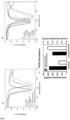
- FDTD optical simulations were performed based on the model of Blu-Ray discs 1-D nanocrystal template coated with a 70 nm Au layer which corresponds to the optimal thickness layer to achieve the minimum reflectivity value in the plasmonic band, and a 1-D nanocrystal template coated in the first step with a 60 nm Au layer (a value below the optimal thickness to achieve the minimum reflectivity value in the plasmonic band) and later with a 10 nm heigh random nanoroughness layer ( Figure 1 ).
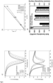
- Optical simulations demonstrate that this extra layer localizes the electromagnetic field near the surface and decreases the evanescent field decay length creating the optimal environment for biosensing of thin biolayers ( Figure 1d and Figure 2a ) in comparison to a flat Au layer.
- this extra layer not only enhances the surface sensitivity of the sensor nearly 2.5-fold when a 10 and 15 nm biolayer is simulated ( Figure 2b and c) but also the addition of this nanoroughness increases the optical absorption (or the minimum reflectivity value in the plasmonic band) due to an increase in scattering phenomena by the nanoroughness, in other words, this nanoroughness promotes a higher energy transfer between the metaplasmonic substrate and the light by light scattering (evident with a wider and deeper plasmonic band).
- the plasmonic metasurfaces were coated with a 15 nm alumina layer by electron beam evaporation to mimic a biolayer, and the plasmonic band displacement was measured.
- the nanoroughness layer increased the biosensing performance up to 1.5-fold, demonstrating that the presence of this second nanoroughness layer has a deep influence on the biosensing performance.
- a first aspect of the invention refers to a plasmonic nanostructure biosensor comprising a substrate and a metal film disposed on the substrate, wherein said metal film is disposed on the substrate under two deposition conditions: one first layer is deposited with a thickness below the optimal plasmonic coupling and a second layer is deposited using oblique angle deposition at a fixed deposition angle.
- the substrate comprises or is made of silicon, silicon dioxide, silicon nitride, glass, diamond, quartz, magnesium fluoride (MgF2), calcium fluoride (CaF2), ZnSe, germanium, or a polymer.
- the substrate is a crystal or a nanocrystal, more preferably a 1-2D nanocrystal template (i.e., Blu-Ray discs 1-D nanocrystals).
- the metal is a noble metal, a transition metal, or an alkali metal.
- the metal comprises or is gold. It is, anyhow, noted that the metals used in the nanoplasmonic structures described herein, are selected on the basis of their surface plasmon properties when an incident light source illuminates their surface.
- the metal used can be thus a noble metal, or any metal selected from the group consisting of gold, rhodium, palladium, silver, osmium, iridium, platinum, titanium, and aluminum.
- the metal is preferably gold
- the first layer has a thickness of less than 70 nm
- the thickness of the second layer is in the range of from 1 to 40 nm
- the total thickness of the first and second layers is in the range of from 65 nm to 100 nm, preferably from 65 nm to 80 nm, more preferably about 70 nm.
- the metal is preferably gold
- the first layer has a thickness of from 40 to 65nm, preferably from 50 nm to 65 nm, more preferably about 60 nm
- the thickness of the second layer is in the range of from 1 to 30 nm, preferably from 1 to 20 nm, more preferably from 1 to 15 nm
- the total thickness of the first and second layers is in the range of from 65 nm to 100 nm, preferably from 65 nm to 80 nm, more preferably about 70 nm.
- the metal disposed on the substrate is gold
- the first layer has a thickness of from 40 to 65nm, preferably from 50 nm to 65 nm, more preferably about 60 nm
- the thickness of the second layer is in the range of from 1 to 30 nm, preferably from 1 to 20 nm, more preferably from 1 to 15 nm
- the total thickness of the first and second layers is in the range of from 65 nm to 80 nm, more preferably about 70 nm.
- the nanoelements can be arranged in any pattern that gives rise to a desired optical property for the nanoplasmonic biosensor, including both periodic patterns and non-periodic patterns, such as pseudo-random and random patterns. Accordingly, in some embodiments of this aspect, the pattern of nanoelements is a periodic pattern. In some embodiments of this aspect, the pattern of nanoelements is a non-periodic pattern, such as a pseudo-random pattern or a random pattern.
- activating the surface of the metal refers to treating it with an activating agent in order to allow, permit or enhance the binding of a nanoelement such as a capture agent.
- the activating agent can be chosen on the basis of the nature of the nanoelement used with the nanoplasmonic structure, for example, whether the nanoelement is a protein or a nucleic acid. Accordingly, in some embodiments, when the nanoelement is a protein, the activating agent used to activate a metal surface is a piranha solution. Therefore, the metallic surface of the plasmonic nanostructure can be functionalized using one or more specific capture agents.
- “functionalization” refers to adding to the surface of the metal of a plasmonic nanostructure according to the invention one or more specific nanoelements.
- the metallic surface is first activated, then functionalized.
- functionalization of a metallic surface can be performed in the absence of activation.
- the nanoelement such as a capture agent used to functionalize a nanoplasmonic nanostructure according to the present invention should have specific binding properties for one or more biomolecular targets.
- a "capture agent” refers to any of a variety of specific binding molecules, including, but not limited to, a DNA oligonucleotide, an RNA oligonucleotide, a peptide, a protein (e.g., transcription factor, antibody or antibody fragment thereof, receptor, a recombinant fusion protein, or enzyme), a small organic molecule, or any combination thereof, that can be immobilized onto the surface of the plasmonic nanostructures described herein.
- the capture agent is immobilized in a periodic fashion.
- one or more specific immobilized capture agents can be arranged in an array at one or more distinct locations on the surface of the plasmonic nanostructure.
- capture agents specific for different biomolecular targets are immobilized at such distinct locations on the surface of a plasmonic structure, such that the structure can be used to detect multiple biomolecular targets in a sample.
- the capture agent is immobilized in a non-periodic or random fashion.
- Such functionalized biosensors are useful for the detection of biomolecular interactions, including, but not limited to, DNA-DNA, DNA-RNA, DNA-protein, RNA-RNA, RNA-protein, and protein-protein interactions.
- a plasmonic nanostructure having a plurality of DNA oligonucleotides immobilized on the surface can be used to detect the presence of a protein, such as a transcription factor, present in a sample contacted with the substrate layer, that binds to one or more of the oligonucleotides.
- the metallic surface of the plasmonic nanostructure described herein is functionalized with a capture agent comprising one or more of a plurality of immobilized DNA oligonucleotides.
- the metallic surface of a plasmonic nanostructure described herein is functionalized with a capture agent comprising one or more of a plurality of immobilized RNA oligonucleotides.
- the metallic surface of a plasmonic nanostructure described herein is functionalized with a capture agent comprising one or more of a plurality of immobilized peptides.
- the metallic surface of a plasmonic nanostructure described herein is functionalized with a capture agent comprising one or more of a plurality of immobilized proteins.
- the protein is an antigen.
- the protein is a polyclonal antibody, monoclonal antibody, single chain antibody (scFv), F(ab) fragment, F(ab')2 fragment, or an Fv fragment.
- the protein is an enzyme, a transcription factor, a receptor, or a recombinant fusion protein.
- a second aspect of the invention refers to a method for manufacturing a plasmonic nanostructure biosensor, wherein the plasmonic nanostructure comprises a substrate and a metal film disposed on the substrate, and wherein the method comprises disposing the metal film on the substrate under two deposition conditions:
- the first layer is deposited under an evaporation flux, preferably deposited under an evaporation flux in an angle of incidence between 70o and 110o, preferably between 80o and 100o, more preferably between 85o and 95o, even more preferably under the normal incidence of evaporation flux.
- the substrate comprises or is made of silicon, silicon dioxide, silicon nitride, glass, diamond, quartz, magnesium fluoride (MgF2), calcium fluoride (CaF2), ZnSe, germanium, or a polymer, preferably the substrate is a crystal or a nanocrystal.
- the metal film comprises or is made of a noble metal, a transition metal, or an alkali metal, or any combination thereof, wherein preferably the metal is gold.
- the substrate is a 1-2D nanocrystal template (i.e., Blu-Ray discs 1-D nanocrystals).
- the second layer is deposited using Glancing Angle Deposition.
- the metal disposed on the substrate is gold
- the first layer is deposited to obtain a thickness of less than 70 nm
- the second layer is deposited to obtain a thickness in the range of from 1 to 40 nm.
- the metal disposed on the substrate is gold
- the first layer is deposited to obtain a thickness of from 40 to 65nm, preferably from 50 nm to 65 nm, more preferably about 60 nm
- the second layer is deposited to obtain a thickness in the range of from 1 to 30 nm, preferably from 1 to 20 nm, more preferably from 1 to 15 nm.
- the metal disposed on the substrate is gold
- the total thickness of the first and second layers is deposited to obtain a thickness in the range of from 65 nm to 100 nm, preferably from 65 nm to 80 nm. Still more preferably, the total thickness of the first and second layers is about 70 nm.
- the metal disposed on the substrate is gold
- the second layer is deposited using Glancing Angle Deposition
- the first layer is deposited to obtain a thickness of from 40 to 65nm, preferably from 50 nm to 65 nm, more preferably about 60 nm
- the second layer is deposited to obtain a thickness in range of from 1 to 30 nm, preferably from 1 to 20 nm, more preferably from 1 to 15 nm
- the total thickness of the first and second layers is in the range of from 65 nm to 80 nm, preferably about 70 nm.
- the second layer is deposited, preferably by using Glancing Angle Deposition, at a fixed deposition angle of less than 90o, preferably between 70o and 90o, more preferably between 80o and 90o. Preferably, about 82o or about 86o.
- the metal film is further functionalized to obtain a plurality of nanoelements arranged in a predefined pattern on top of the metal film, wherein each of said nanoelements has a dimension of less than 100 nm, preferably between 1 to 15 nm, more preferably between 5 and 10 nm. It is noted that such nanoelements are preferably capture elements as defined and as specified in the first aspect of the invention.
- a third aspect of the invention refers to a plasmonic nanostructure biosensor obtained according to the method of the second aspect of the invention or according to any of its preferred embodiments.
- a fourth aspect of the invention refers to the in vitro use of the plasmonic nanostructure according to the first aspect of the invention or according to any of its preferred embodiments or the plasmonic nanostructure according to the third aspect of the invention, for detecting one or more biomolecular targets, wherein preferably the biorecognition event is below 100 nm, preferably between 10 to 15 nm.
- a fifth aspect of the invention refers to a plasmonic nanostructure biosensor system for detecting one or more biomolecular targets, preferably comprising:
- the device for contacting one or more samples comprises a fluidic system.
- a sixth aspect of the invention refers to a method for detecting one or more biomolecular targets comprising:
- the biomolecular target is a eukaryotic cell, a eukaryotic cellular component, a prokaryotic cell, a prokaryotic cellular component, a viral particle, a protein, an oligonucleotide, a prion, a toxin, or any combination thereof.
- said collected light comprises light in a transmission mode, in a reflection mode, or a combination thereof.
- the step of measuring displaced light comprises measuring light over a spectral range selected to comprise at least one plasmon band.
- the change in the measurement of the displaced light before and after the contacting is a resonance peak shift, a change in a resonance peak intensity, a broadening of a resonance peak, a distortion in the resonance of peak, or a change in refractive index.
- FDTD Simulations 3D FDTD simulations were carried out using commercial software (FDTD solution, Lumerical, Inc., Vancouver, Canada). Structural parameters of the Blu-ray discs utilized in the simulations (i.e., a grating period of 320 nm, grating width of 100 nm, and a height of 20 nm) were as claimed to Atomic Force Microscopy (AFM) images from previous results (López et al., 2018) . Periodic boundary conditions were used on the x and y-axis, and the perfectly matched layers (PML) approach was used on the z-axis, with a uniform mesh size of 2 nm on all axes.
- AFM Atomic Force Microscopy
- the target has 5N (99.9995%) purity, 50 mm diameter and 50W DC-MF (direct current-medium frequency) power supply was used.
- the base vacuum and operating pressure were 5 ⁇ 10 -6 mbar and 8 ⁇ 10 -3 mbar, respectively.
- a 70 nm thick layer of gold was deposited without GLAD
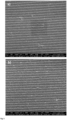
- a first 60 nm layer without GLAD was deposited and after, a nanoroughness layer of 5 to 15 nm height was deposited with GLAD angles of 82 and 86°
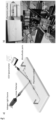
- the microfluidic system for carrying out the detection in solution was developed using a patterned microfluidic multichannel in a 140 ⁇ m thick double-sided adhesive tape sheet (Mcs-foil-008, Microfluidic ChipShop GmbH, Germany).
- the proposed design integrates two sensing regions to allow multiplexed biodetection.
- a 2 mm tick patterned polymethyl methacrylate (PMMA) lid was added as a cover to facilitate the fluidic tubes' connection.
Landscapes
- Chemical & Material Sciences (AREA)
- Engineering & Computer Science (AREA)
- Nanotechnology (AREA)
- Physics & Mathematics (AREA)
- Health & Medical Sciences (AREA)
- Life Sciences & Earth Sciences (AREA)
- Analytical Chemistry (AREA)
- Biochemistry (AREA)
- General Health & Medical Sciences (AREA)
- General Physics & Mathematics (AREA)
- Immunology (AREA)
- Pathology (AREA)
- Investigating Or Analysing Materials By Optical Means (AREA)
Priority Applications (6)
| Application Number | Priority Date | Filing Date | Title |
|---|---|---|---|
| EP23382034.9A EP4403901A1 (de) | 2023-01-17 | 2023-01-17 | Zweistufiges verfahren zur herstellung von plasmonischen nanostrukturen für plasmonisches biosensing |
| PCT/EP2024/051063 WO2024153708A1 (en) | 2023-01-17 | 2024-01-17 | A two-step method for manufacturing plasmonic nanostructures for plasmonic biosensing |
| JP2025562867A JP2026504218A (ja) | 2023-01-17 | 2024-01-17 | プラズモンバイオセンシング用のプラズモンナノ構造を製造する二段階法 |
| EP24700809.7A EP4652445A1 (de) | 2023-01-17 | 2024-01-17 | Zweistufiges verfahren zur herstellung von plasmonischen nanostrukturen für plasmonisches biosensing |
| CN202480019800.XA CN120883044A (zh) | 2023-01-17 | 2024-01-17 | 制造用于等离激元生物传感的等离激元纳米结构的两步方法 |
| KR1020257026758A KR20250135255A (ko) | 2023-01-17 | 2024-01-17 | 플라즈모닉 바이오센싱을 위한 플라즈모닉 나노구조체를 제조하기 위한 2-단계 방법 |
Applications Claiming Priority (1)
| Application Number | Priority Date | Filing Date | Title |
|---|---|---|---|
| EP23382034.9A EP4403901A1 (de) | 2023-01-17 | 2023-01-17 | Zweistufiges verfahren zur herstellung von plasmonischen nanostrukturen für plasmonisches biosensing |
Publications (1)
| Publication Number | Publication Date |
|---|---|
| EP4403901A1 true EP4403901A1 (de) | 2024-07-24 |
Family
ID=84982569
Family Applications (2)
| Application Number | Title | Priority Date | Filing Date |
|---|---|---|---|
| EP23382034.9A Withdrawn EP4403901A1 (de) | 2023-01-17 | 2023-01-17 | Zweistufiges verfahren zur herstellung von plasmonischen nanostrukturen für plasmonisches biosensing |
| EP24700809.7A Pending EP4652445A1 (de) | 2023-01-17 | 2024-01-17 | Zweistufiges verfahren zur herstellung von plasmonischen nanostrukturen für plasmonisches biosensing |
Family Applications After (1)
| Application Number | Title | Priority Date | Filing Date |
|---|---|---|---|
| EP24700809.7A Pending EP4652445A1 (de) | 2023-01-17 | 2024-01-17 | Zweistufiges verfahren zur herstellung von plasmonischen nanostrukturen für plasmonisches biosensing |
Country Status (5)
| Country | Link |
|---|---|
| EP (2) | EP4403901A1 (de) |
| JP (1) | JP2026504218A (de) |
| KR (1) | KR20250135255A (de) |
| CN (1) | CN120883044A (de) |
| WO (1) | WO2024153708A1 (de) |
-
2023
- 2023-01-17 EP EP23382034.9A patent/EP4403901A1/de not_active Withdrawn
-
2024
- 2024-01-17 CN CN202480019800.XA patent/CN120883044A/zh active Pending
- 2024-01-17 JP JP2025562867A patent/JP2026504218A/ja active Pending
- 2024-01-17 WO PCT/EP2024/051063 patent/WO2024153708A1/en not_active Ceased
- 2024-01-17 EP EP24700809.7A patent/EP4652445A1/de active Pending
- 2024-01-17 KR KR1020257026758A patent/KR20250135255A/ko active Pending
Non-Patent Citations (15)
| Title |
|---|
| BADSHAH M A ET AL: "Enhancing the Sensitivity of a Surface Plasmon Resonance Sensor with Glancing Angle Deposited Nanostructures", PLASMONICS, SPRINGER US, BOSTON, vol. 15, no. 6, 2 August 2020 (2020-08-02), pages 2161 - 2168, XP037284922, ISSN: 1557-1955, [retrieved on 20200802], DOI: 10.1007/S11468-020-01245-0 * |
| BELUSHKIN, ALEXANDER ET AL.: "Rapid and digital detection of inflammatory biomarkers enabled by a novel portable nanoplasmonic imager", SMALL, vol. 16, no. 3, 2020, pages 1906108 |
| GAROLI, DENIS ET AL.: "Nanoporous gold metamaterials for high sensitivity plasmonic sensing", NANOSCALE HORIZONS, vol. 4, no. 5, 2019, pages 1153 - 1157 |
| KIM N-H ET AL: "Improved biomolecular detection based on a plasmonic nanoporous gold film fabricated by oblique angle deposition", OPTICS EXPRESS, vol. 23, no. 14, 10 July 2015 (2015-07-10), pages 18777, XP093040603, DOI: 10.1364/OE.23.018777 * |
| LOPEZ, GERARDO A. ET AL.: "Recent advances in nanoplasmonic biosensors: applications and lab-on-a-chip integration", NANOPHOTONICS, vol. 6, no. 1, 2017, pages 123 - 136, XP055913593, DOI: 10.1515/nanoph-2016-0101 |
| LÓPEZ-MUÑOZ G A ET AL: "Gold/silver/gold trilayer films on nanostructured polycarbonate substrates for direct and label-free nanoplasmonic biosensing", JOURNAL OF BIOPHOTONICS, vol. 11, no. 8, 24 May 2018 (2018-05-24), DE, XP093040502, ISSN: 1864-063X, Retrieved from the Internet <URL:https://onlinelibrary.wiley.com/doi/full-xml/10.1002/jbio.201800043> [retrieved on 20230420], DOI: 10.1002/jbio.201800043 * |
| LÓPEZ-MUÑOZ G A ET AL: "Plasmonic nanocrystals on polycarbonate substrates for direct and label-free biodetection of Interleukin-6 in bioengineered 3D skeletal muscles", NANOPHOTONICS, vol. 10, no. 18, 8 October 2021 (2021-10-08), pages 4477 - 4488, XP093040501, DOI: 10.1515/nanoph-2021-0426 * |
| LÓPEZ-MUÑOZ G A ET AL: "Scalable, Lithography-Free Plasmonic Metasurfaces by Nano-Patterned/Sculpted Thin Films for Biosensing", FRONTIERS IN SENSORS, vol. 3, 27 June 2022 (2022-06-27), XP093040662, DOI: 10.3389/fsens.2022.945525 * |
| LOPEZ-MUNOZ GAESTEVEZ MCVAZQUEZ-GARCIA MBERENGUEL-ALONSO MALONSO-CHAMARRO JHOMS-CORBERA ALECHUGA LM: "Gold/silver/gold trilayer films on nanostructured polycarbonate substrates for direct and label-free nanoplasmonic biosensing", J BIOPHOTONICS, vol. 11, 2018, pages e201800043, Retrieved from the Internet <URL:https://doi.org/10.1002/jbio.201800043> |
| LOPEZ-MUNOZ, GERARDO A. ET AL.: "Plasmonic nanocrystals on polycarbonate substrates for direct and label-free biodetection of Interleukin-6 in bioengineered 3D skeletal muscles", NANOPHOTONICS, vol. 10, no. 18, 2021, pages 4477 - 4488 |
| SPACKOVA, BARBORAMARIA LAURA ERMINIJIRI HOMOLA: "High-performance biosensor exploiting a light guidance in sparse arrays of metal nanoparticles", OPTICS LETTERS, vol. 44, no. 7, 2019, pages 1568 - 1571 |
| SULTANOVA NKASAROVA SNIKOLOV I: "Dispersion properties of optical polymers", ACTA PHYS POL A, vol. 116, 2009, pages 585 - 587, Retrieved from the Internet <URL:https://doi.org/10.12693/APhysPolA.116.585> |
| VILA J C ET AL: "Disposable Polymeric Nanostructured Plasmonic Biosensors for Cell Culture Adhesion Monitoring", FRONTIERS IN BIOENGINEERING AND BIOTECHNOLOGY, vol. 9, 6 December 2021 (2021-12-06), XP093040682, DOI: 10.3389/fbioe.2021.799325 * |
| WAKAKI MKUDO KSHIBUYA, T: "Physical properties and data of optical materials", 2007, CRC PRESS |
| XU YBAI PZHOU XAKIMOV YPNG CEANG LKKNOLL WWU, L: "Optical Refractive Index Sensors with Plasmonic and Photonic Structures: Promising and Inconvenient Truth", ADV OPT MATER, vol. 7, 2019, pages 31 - 33, Retrieved from the Internet <URL:https://doi.org/10.1002/adom.201801433> |
Also Published As
| Publication number | Publication date |
|---|---|
| CN120883044A (zh) | 2025-10-31 |
| KR20250135255A (ko) | 2025-09-12 |
| JP2026504218A (ja) | 2026-02-03 |
| EP4652445A1 (de) | 2025-11-26 |
| WO2024153708A1 (en) | 2024-07-25 |
Similar Documents
| Publication | Publication Date | Title |
|---|---|---|
| Mazzotta et al. | Influence of the evanescent field decay length on the sensitivity of plasmonic nanodisks and nanoholes | |
| Shin et al. | A plasmonic biosensor array by block copolymer lithography | |
| US7705280B2 (en) | Multispectral plasmonic crystal sensors | |
| Kambhampati et al. | Novel Silicon Dioxide Sol− Gel Films for Potential Sensor Applications: A Surface Plasmon Resonance Study | |
| Hoa et al. | Enhanced SPR response from patterned immobilization of surface bioreceptors on nano-gratings | |
| Singh et al. | Surface plasmon resonance enhanced transmission of light through gold-coated diffraction gratings | |
| US20070222995A1 (en) | Artifact having a textured metal surface with nanometer-scale features and method for fabricating same | |
| Zhang et al. | Fabrication of gold-coated PDMS surfaces with arrayed triangular micro/nanopyramids for use as SERS substrates | |
| KR101029115B1 (ko) | 금속 증착형 다공성 산화 알루미늄 바이오칩 및 그 제조방법 | |
| Zhang et al. | Plasmonic metal nanostructure array by glancing angle deposition for biosensing application | |
| Arai et al. | An optical biosensor based on localized surface plasmon resonance of silver nanostructured films | |
| Sohrabi et al. | Plasmonic structures for phase-sensitive ellipsometry biosensing: a review | |
| Ekgasit et al. | Fluorescence intensity in surface-plasmon field-enhanced fluorescence spectroscopy | |
| Byun et al. | Investigation of the profile effect on the sensitivity enhancement of nanowire-mediated localized surface plasmon resonance biosensors | |
| Byun | Development of nanostructured plasmonic substrates for enhanced optical biosensing | |
| US9739713B2 (en) | Microstructured chip comprising convex surfaces for surface plasmon resonance analysis, analysis device containing said microstructured chip and use of said device | |
| EP4403901A1 (de) | Zweistufiges verfahren zur herstellung von plasmonischen nanostrukturen für plasmonisches biosensing | |
| Ferré-Borrull et al. | Optical properties of nanoporous anodic alumina and derived applications | |
| Shibata et al. | Optimization of metal quality for grating coupled surface plasmon resonance | |
| Lee et al. | Unconventional methods for fabricating nanostructures toward high-fidelity sensors | |
| Sai Sathish et al. | Solution-deposited thin silver films on plastic surfaces for low-cost applications in plasmon-coupled emission sensors | |
| Jung et al. | Development of a large-area plasmonic sensor substrate with dielectric subwavelength gratings using nanoimprint lithography | |
| Descrovi et al. | New sensing strategies based on surface modes in photonic crystals | |
| Uchino et al. | Graphene-based flexible SERS substrates with Ag nanohole structures for biochemical sensing | |
| Byun et al. | Effect of metallic nanowires on the sensitivity enhancement of surface plasmon resonance biosensors |
Legal Events
| Date | Code | Title | Description |
|---|---|---|---|
| PUAI | Public reference made under article 153(3) epc to a published international application that has entered the european phase |
Free format text: ORIGINAL CODE: 0009012 |
|
| STAA | Information on the status of an ep patent application or granted ep patent |
Free format text: STATUS: THE APPLICATION HAS BEEN PUBLISHED |
|
| AK | Designated contracting states |
Kind code of ref document: A1 Designated state(s): AL AT BE BG CH CY CZ DE DK EE ES FI FR GB GR HR HU IE IS IT LI LT LU LV MC ME MK MT NL NO PL PT RO RS SE SI SK SM TR |
|
| STAA | Information on the status of an ep patent application or granted ep patent |
Free format text: STATUS: THE APPLICATION IS DEEMED TO BE WITHDRAWN |
|
| 18D | Application deemed to be withdrawn |
Effective date: 20250125 |