EP4401313A1 - Photovoltaic inverter, direct current conversion circuit, and inverter circuit - Google Patents
Photovoltaic inverter, direct current conversion circuit, and inverter circuit Download PDFInfo
- Publication number
- EP4401313A1 EP4401313A1 EP24151521.2A EP24151521A EP4401313A1 EP 4401313 A1 EP4401313 A1 EP 4401313A1 EP 24151521 A EP24151521 A EP 24151521A EP 4401313 A1 EP4401313 A1 EP 4401313A1
- Authority
- EP
- European Patent Office
- Prior art keywords
- switch transistor
- direct current
- inverter
- pin
- current conversion
- Prior art date
- Legal status (The legal status is an assumption and is not a legal conclusion. Google has not performed a legal analysis and makes no representation as to the accuracy of the status listed.)
- Pending
Links
Images




Classifications
-
- H—ELECTRICITY
- H03—ELECTRONIC CIRCUITRY
- H03K—PULSE TECHNIQUE
- H03K17/00—Electronic switching or gating, i.e. not by contact-making and –breaking
- H03K17/16—Modifications for eliminating interference voltages or currents
-
- H—ELECTRICITY
- H02—GENERATION; CONVERSION OR DISTRIBUTION OF ELECTRIC POWER
- H02J—ELECTRIC POWER NETWORKS; CIRCUIT ARRANGEMENTS OR SYSTEMS FOR SUPPLYING OR DISTRIBUTING ELECTRIC POWER; SYSTEMS FOR STORING ELECTRIC ENERGY
- H02J3/00—Circuit arrangements for AC mains or AC distribution networks
- H02J3/38—Arrangements for feeding a single network from two or more generators or sources in parallel; Arrangements for feeding already energised networks from additional generators or sources in parallel
-
- H—ELECTRICITY
- H02—GENERATION; CONVERSION OR DISTRIBUTION OF ELECTRIC POWER
- H02J—ELECTRIC POWER NETWORKS; CIRCUIT ARRANGEMENTS OR SYSTEMS FOR SUPPLYING OR DISTRIBUTING ELECTRIC POWER; SYSTEMS FOR STORING ELECTRIC ENERGY
- H02J3/00—Circuit arrangements for AC mains or AC distribution networks
- H02J3/38—Arrangements for feeding a single network from two or more generators or sources in parallel; Arrangements for feeding already energised networks from additional generators or sources in parallel
- H02J3/381—Dispersed generators
-
- H—ELECTRICITY
- H02—GENERATION; CONVERSION OR DISTRIBUTION OF ELECTRIC POWER
- H02M—APPARATUS FOR CONVERSION BETWEEN AC AND AC, BETWEEN AC AND DC, OR BETWEEN DC AND DC, AND FOR USE WITH MAINS OR SIMILAR POWER SUPPLY SYSTEMS; CONVERSION OF DC OR AC INPUT POWER INTO SURGE OUTPUT POWER; CONTROL OR REGULATION THEREOF
- H02M1/00—Details of apparatus for conversion
- H02M1/0003—Details of control, feedback or regulation circuits
- H02M1/0038—Circuits or arrangements for suppressing, e.g. by masking incorrect turn-on or turn-off signals, e.g. due to current spikes in current mode control
-
- H—ELECTRICITY
- H02—GENERATION; CONVERSION OR DISTRIBUTION OF ELECTRIC POWER
- H02M—APPARATUS FOR CONVERSION BETWEEN AC AND AC, BETWEEN AC AND DC, OR BETWEEN DC AND DC, AND FOR USE WITH MAINS OR SIMILAR POWER SUPPLY SYSTEMS; CONVERSION OF DC OR AC INPUT POWER INTO SURGE OUTPUT POWER; CONTROL OR REGULATION THEREOF
- H02M1/00—Details of apparatus for conversion
- H02M1/0048—Circuits or arrangements for reducing losses
-
- H—ELECTRICITY
- H02—GENERATION; CONVERSION OR DISTRIBUTION OF ELECTRIC POWER
- H02M—APPARATUS FOR CONVERSION BETWEEN AC AND AC, BETWEEN AC AND DC, OR BETWEEN DC AND DC, AND FOR USE WITH MAINS OR SIMILAR POWER SUPPLY SYSTEMS; CONVERSION OF DC OR AC INPUT POWER INTO SURGE OUTPUT POWER; CONTROL OR REGULATION THEREOF
- H02M1/00—Details of apparatus for conversion
- H02M1/0048—Circuits or arrangements for reducing losses
- H02M1/0054—Transistor switching losses
-
- H—ELECTRICITY
- H02—GENERATION; CONVERSION OR DISTRIBUTION OF ELECTRIC POWER
- H02M—APPARATUS FOR CONVERSION BETWEEN AC AND AC, BETWEEN AC AND DC, OR BETWEEN DC AND DC, AND FOR USE WITH MAINS OR SIMILAR POWER SUPPLY SYSTEMS; CONVERSION OF DC OR AC INPUT POWER INTO SURGE OUTPUT POWER; CONTROL OR REGULATION THEREOF
- H02M1/00—Details of apparatus for conversion
- H02M1/08—Circuits specially adapted for the generation of control voltages for semiconductor devices incorporated in static converters
-
- H—ELECTRICITY
- H02—GENERATION; CONVERSION OR DISTRIBUTION OF ELECTRIC POWER
- H02M—APPARATUS FOR CONVERSION BETWEEN AC AND AC, BETWEEN AC AND DC, OR BETWEEN DC AND DC, AND FOR USE WITH MAINS OR SIMILAR POWER SUPPLY SYSTEMS; CONVERSION OF DC OR AC INPUT POWER INTO SURGE OUTPUT POWER; CONTROL OR REGULATION THEREOF
- H02M1/00—Details of apparatus for conversion
- H02M1/08—Circuits specially adapted for the generation of control voltages for semiconductor devices incorporated in static converters
- H02M1/088—Circuits specially adapted for the generation of control voltages for semiconductor devices incorporated in static converters for the simultaneous control of series or parallel connected semiconductor devices
-
- H—ELECTRICITY
- H02—GENERATION; CONVERSION OR DISTRIBUTION OF ELECTRIC POWER
- H02M—APPARATUS FOR CONVERSION BETWEEN AC AND AC, BETWEEN AC AND DC, OR BETWEEN DC AND DC, AND FOR USE WITH MAINS OR SIMILAR POWER SUPPLY SYSTEMS; CONVERSION OF DC OR AC INPUT POWER INTO SURGE OUTPUT POWER; CONTROL OR REGULATION THEREOF
- H02M3/00—Conversion of DC power input into DC power output
- H02M3/02—Conversion of DC power input into DC power output without intermediate conversion into AC
- H02M3/04—Conversion of DC power input into DC power output without intermediate conversion into AC by static converters
- H02M3/10—Conversion of DC power input into DC power output without intermediate conversion into AC by static converters using discharge tubes with control electrode or semiconductor devices with control electrode
-
- H—ELECTRICITY
- H02—GENERATION; CONVERSION OR DISTRIBUTION OF ELECTRIC POWER
- H02M—APPARATUS FOR CONVERSION BETWEEN AC AND AC, BETWEEN AC AND DC, OR BETWEEN DC AND DC, AND FOR USE WITH MAINS OR SIMILAR POWER SUPPLY SYSTEMS; CONVERSION OF DC OR AC INPUT POWER INTO SURGE OUTPUT POWER; CONTROL OR REGULATION THEREOF
- H02M3/00—Conversion of DC power input into DC power output
- H02M3/02—Conversion of DC power input into DC power output without intermediate conversion into AC
- H02M3/04—Conversion of DC power input into DC power output without intermediate conversion into AC by static converters
- H02M3/10—Conversion of DC power input into DC power output without intermediate conversion into AC by static converters using discharge tubes with control electrode or semiconductor devices with control electrode
- H02M3/145—Conversion of DC power input into DC power output without intermediate conversion into AC by static converters using discharge tubes with control electrode or semiconductor devices with control electrode using devices of a triode or transistor type requiring continuous application of a control signal
- H02M3/155—Conversion of DC power input into DC power output without intermediate conversion into AC by static converters using discharge tubes with control electrode or semiconductor devices with control electrode using devices of a triode or transistor type requiring continuous application of a control signal using semiconductor devices only
- H02M3/156—Conversion of DC power input into DC power output without intermediate conversion into AC by static converters using discharge tubes with control electrode or semiconductor devices with control electrode using devices of a triode or transistor type requiring continuous application of a control signal using semiconductor devices only with automatic control of output voltage or current, e.g. switching regulators
- H02M3/158—Conversion of DC power input into DC power output without intermediate conversion into AC by static converters using discharge tubes with control electrode or semiconductor devices with control electrode using devices of a triode or transistor type requiring continuous application of a control signal using semiconductor devices only with automatic control of output voltage or current, e.g. switching regulators including plural semiconductor devices as final control devices for a single load
- H02M3/1584—Conversion of DC power input into DC power output without intermediate conversion into AC by static converters using discharge tubes with control electrode or semiconductor devices with control electrode using devices of a triode or transistor type requiring continuous application of a control signal using semiconductor devices only with automatic control of output voltage or current, e.g. switching regulators including plural semiconductor devices as final control devices for a single load with a plurality of power processing stages connected in parallel
-
- H—ELECTRICITY
- H02—GENERATION; CONVERSION OR DISTRIBUTION OF ELECTRIC POWER
- H02M—APPARATUS FOR CONVERSION BETWEEN AC AND AC, BETWEEN AC AND DC, OR BETWEEN DC AND DC, AND FOR USE WITH MAINS OR SIMILAR POWER SUPPLY SYSTEMS; CONVERSION OF DC OR AC INPUT POWER INTO SURGE OUTPUT POWER; CONTROL OR REGULATION THEREOF
- H02M7/00—Conversion of AC power input into DC power output; Conversion of DC power input into AC power output
- H02M7/42—Conversion of DC power input into AC power output without possibility of reversal
- H02M7/44—Conversion of DC power input into AC power output without possibility of reversal by static converters
- H02M7/48—Conversion of DC power input into AC power output without possibility of reversal by static converters using discharge tubes with control electrode or semiconductor devices with control electrode
-
- H—ELECTRICITY
- H02—GENERATION; CONVERSION OR DISTRIBUTION OF ELECTRIC POWER
- H02M—APPARATUS FOR CONVERSION BETWEEN AC AND AC, BETWEEN AC AND DC, OR BETWEEN DC AND DC, AND FOR USE WITH MAINS OR SIMILAR POWER SUPPLY SYSTEMS; CONVERSION OF DC OR AC INPUT POWER INTO SURGE OUTPUT POWER; CONTROL OR REGULATION THEREOF
- H02M7/00—Conversion of AC power input into DC power output; Conversion of DC power input into AC power output
- H02M7/42—Conversion of DC power input into AC power output without possibility of reversal
- H02M7/44—Conversion of DC power input into AC power output without possibility of reversal by static converters
- H02M7/48—Conversion of DC power input into AC power output without possibility of reversal by static converters using discharge tubes with control electrode or semiconductor devices with control electrode
- H02M7/493—Conversion of DC power input into AC power output without possibility of reversal by static converters using discharge tubes with control electrode or semiconductor devices with control electrode the static converters being arranged for operation in parallel
-
- H—ELECTRICITY
- H02—GENERATION; CONVERSION OR DISTRIBUTION OF ELECTRIC POWER
- H02M—APPARATUS FOR CONVERSION BETWEEN AC AND AC, BETWEEN AC AND DC, OR BETWEEN DC AND DC, AND FOR USE WITH MAINS OR SIMILAR POWER SUPPLY SYSTEMS; CONVERSION OF DC OR AC INPUT POWER INTO SURGE OUTPUT POWER; CONTROL OR REGULATION THEREOF
- H02M7/00—Conversion of AC power input into DC power output; Conversion of DC power input into AC power output
- H02M7/42—Conversion of DC power input into AC power output without possibility of reversal
- H02M7/44—Conversion of DC power input into AC power output without possibility of reversal by static converters
- H02M7/48—Conversion of DC power input into AC power output without possibility of reversal by static converters using discharge tubes with control electrode or semiconductor devices with control electrode
- H02M7/53—Conversion of DC power input into AC power output without possibility of reversal by static converters using discharge tubes with control electrode or semiconductor devices with control electrode using devices of a triode or transistor type requiring continuous application of a control signal
- H02M7/537—Conversion of DC power input into AC power output without possibility of reversal by static converters using discharge tubes with control electrode or semiconductor devices with control electrode using devices of a triode or transistor type requiring continuous application of a control signal using semiconductor devices only, e.g. single switched pulse inverters
-
- H—ELECTRICITY
- H02—GENERATION; CONVERSION OR DISTRIBUTION OF ELECTRIC POWER
- H02S—GENERATION OF ELECTRIC POWER BY CONVERSION OF INFRARED RADIATION, VISIBLE LIGHT OR ULTRAVIOLET LIGHT, e.g. USING PHOTOVOLTAIC [PV] MODULES
- H02S40/00—Components or accessories in combination with PV modules, not provided for in groups H02S10/00 - H02S30/00
- H02S40/30—Electrical components
-
- H—ELECTRICITY
- H03—ELECTRONIC CIRCUITRY
- H03K—PULSE TECHNIQUE
- H03K17/00—Electronic switching or gating, i.e. not by contact-making and –breaking
- H03K17/04—Modifications for accelerating switching
-
- H—ELECTRICITY
- H03—ELECTRONIC CIRCUITRY
- H03K—PULSE TECHNIQUE
- H03K17/00—Electronic switching or gating, i.e. not by contact-making and –breaking
- H03K17/04—Modifications for accelerating switching
- H03K17/0406—Modifications for accelerating switching in composite switches
-
- H—ELECTRICITY
- H03—ELECTRONIC CIRCUITRY
- H03K—PULSE TECHNIQUE
- H03K17/00—Electronic switching or gating, i.e. not by contact-making and –breaking
- H03K17/04—Modifications for accelerating switching
- H03K17/041—Modifications for accelerating switching without feedback from the output circuit to the control circuit
-
- H—ELECTRICITY
- H02—GENERATION; CONVERSION OR DISTRIBUTION OF ELECTRIC POWER
- H02J—ELECTRIC POWER NETWORKS; CIRCUIT ARRANGEMENTS OR SYSTEMS FOR SUPPLYING OR DISTRIBUTING ELECTRIC POWER; SYSTEMS FOR STORING ELECTRIC ENERGY
- H02J2101/00—Supply or distribution of decentralised, dispersed or local electric power generation
- H02J2101/20—Dispersed power generation using renewable energy sources
- H02J2101/22—Solar energy
- H02J2101/24—Photovoltaics
-
- H—ELECTRICITY
- H02—GENERATION; CONVERSION OR DISTRIBUTION OF ELECTRIC POWER
- H02M—APPARATUS FOR CONVERSION BETWEEN AC AND AC, BETWEEN AC AND DC, OR BETWEEN DC AND DC, AND FOR USE WITH MAINS OR SIMILAR POWER SUPPLY SYSTEMS; CONVERSION OF DC OR AC INPUT POWER INTO SURGE OUTPUT POWER; CONTROL OR REGULATION THEREOF
- H02M1/00—Details of apparatus for conversion
- H02M1/0003—Details of control, feedback or regulation circuits
- H02M1/0006—Arrangements for supplying an adequate voltage to the control circuit of converters
-
- H—ELECTRICITY
- H02—GENERATION; CONVERSION OR DISTRIBUTION OF ELECTRIC POWER
- H02M—APPARATUS FOR CONVERSION BETWEEN AC AND AC, BETWEEN AC AND DC, OR BETWEEN DC AND DC, AND FOR USE WITH MAINS OR SIMILAR POWER SUPPLY SYSTEMS; CONVERSION OF DC OR AC INPUT POWER INTO SURGE OUTPUT POWER; CONTROL OR REGULATION THEREOF
- H02M3/00—Conversion of DC power input into DC power output
- H02M3/02—Conversion of DC power input into DC power output without intermediate conversion into AC
- H02M3/04—Conversion of DC power input into DC power output without intermediate conversion into AC by static converters
- H02M3/10—Conversion of DC power input into DC power output without intermediate conversion into AC by static converters using discharge tubes with control electrode or semiconductor devices with control electrode
- H02M3/145—Conversion of DC power input into DC power output without intermediate conversion into AC by static converters using discharge tubes with control electrode or semiconductor devices with control electrode using devices of a triode or transistor type requiring continuous application of a control signal
- H02M3/155—Conversion of DC power input into DC power output without intermediate conversion into AC by static converters using discharge tubes with control electrode or semiconductor devices with control electrode using devices of a triode or transistor type requiring continuous application of a control signal using semiconductor devices only
- H02M3/156—Conversion of DC power input into DC power output without intermediate conversion into AC by static converters using discharge tubes with control electrode or semiconductor devices with control electrode using devices of a triode or transistor type requiring continuous application of a control signal using semiconductor devices only with automatic control of output voltage or current, e.g. switching regulators
-
- H—ELECTRICITY
- H02—GENERATION; CONVERSION OR DISTRIBUTION OF ELECTRIC POWER
- H02M—APPARATUS FOR CONVERSION BETWEEN AC AND AC, BETWEEN AC AND DC, OR BETWEEN DC AND DC, AND FOR USE WITH MAINS OR SIMILAR POWER SUPPLY SYSTEMS; CONVERSION OF DC OR AC INPUT POWER INTO SURGE OUTPUT POWER; CONTROL OR REGULATION THEREOF
- H02M7/00—Conversion of AC power input into DC power output; Conversion of DC power input into AC power output
- H02M7/42—Conversion of DC power input into AC power output without possibility of reversal
- H02M7/44—Conversion of DC power input into AC power output without possibility of reversal by static converters
- H02M7/48—Conversion of DC power input into AC power output without possibility of reversal by static converters using discharge tubes with control electrode or semiconductor devices with control electrode
- H02M7/483—Converters with outputs that each can have more than two voltages levels
- H02M7/487—Neutral point clamped inverters
-
- H—ELECTRICITY
- H03—ELECTRONIC CIRCUITRY
- H03K—PULSE TECHNIQUE
- H03K2217/00—Indexing scheme related to electronic switching or gating, i.e. not by contact-making or -breaking covered by H03K17/00
- H03K2217/0072—Low side switches, i.e. the lower potential [DC] or neutral wire [AC] being directly connected to the switch and not via the load
-
- Y—GENERAL TAGGING OF NEW TECHNOLOGICAL DEVELOPMENTS; GENERAL TAGGING OF CROSS-SECTIONAL TECHNOLOGIES SPANNING OVER SEVERAL SECTIONS OF THE IPC; TECHNICAL SUBJECTS COVERED BY FORMER USPC CROSS-REFERENCE ART COLLECTIONS [XRACs] AND DIGESTS
- Y02—TECHNOLOGIES OR APPLICATIONS FOR MITIGATION OR ADAPTATION AGAINST CLIMATE CHANGE
- Y02E—REDUCTION OF GREENHOUSE GAS [GHG] EMISSIONS, RELATED TO ENERGY GENERATION, TRANSMISSION OR DISTRIBUTION
- Y02E10/00—Energy generation through renewable energy sources
- Y02E10/50—Photovoltaic [PV] energy
- Y02E10/56—Power conversion systems, e.g. maximum power point trackers
Definitions
- This application relates to the field of power electronics, and in particular, to a photovoltaic inverter, a direct current conversion circuit, and an inverter circuit.
- power supply equipment such as a switching power supply and an inverter
- efficiency and thermal design are important aspects in design of the power supply equipment.
- Power devices such as various switch transistors and transistors
- Loss reduction of the power devices plays a key role in the efficiency and thermal design of the power supply equipment. So far, most switch transistors and transistors are three-pin (or 3PIN) devices with a drive part compared with diodes. For a three-pin device, interaction between a power loop and a drive voltage signal is more sensitive.
- stray inductance of a source or an emitter of a switch transistor plus switch current slope generates a voltage signal opposite to a drive voltage signal of a transistor, which reduces a switching speed of the switch transistor and increases a switching loss of each switching cycle, resulting in an increase in heat consumption of power supply equipment. Therefore, how to resolve a problem of an increase of a working loss of the power supply equipment due to reduction of the switching speed of the switch transistor caused by interaction between the power loop and the drive voltage signal of the switch transistor and the transistor in the power supply equipment is one of the technical problems that need to be urgently resolved currently.
- Embodiments of this application provide a photovoltaic inverter, a direct current conversion circuit, and an inverter circuit, to avoid interference on a drive voltage by parasitic inductance generated based on a power current of a switch transistor, thereby increasing an overall switching speed of the switch transistor in the photovoltaic inverter, and reducing a working loss of the photovoltaic inverter.
- this application provides a photovoltaic inverter.
- the photovoltaic inverter includes a direct current conversion circuit and an inverter circuit. An input end of the direct current conversion circuit is configured to connect to a direct current power supply. An output end of the direct current conversion circuit is configured to connect to an input end of the inverter circuit. An output end of the inverter circuit is configured to couple to an alternating current power grid.
- the direct current conversion circuit includes a plurality of direct current conversion units connected in parallel.
- the inverter circuit includes a plurality of inverter units.
- the photovoltaic inverter further includes a drive power supply and a plurality of drive units.
- a first input end and a second input end of each drive unit are respectively connected to a positive electrode and a negative electrode of the drive power supply.
- Each direct current conversion unit and each inverter unit further include a switch transistor.
- An output end of any drive unit is connected to a first end of one switch transistor in the direct current conversion unit or is connected to a first end of one target switch transistor in a plurality of switch transistors of an inverter unit associated with the any drive unit.
- At least one of the plurality of direct current conversion units includes a four-pin switch transistor or a target switch transistor included in at least one of the plurality of inverter units is a four-pin switch transistor.
- a fourth end of the four-pin switch transistor is connected to a first end and a second end of the four-pin switch transistor.
- the fourth end of the four-pin switch transistor is coupled to a first input end and a second input end of a target drive unit connected to the at least one direct current conversion unit or the at least one inverter unit.
- the photovoltaic inverter is configured to separate, through the fourth end of the four-pin switch transistor, a power current outputted from the second end of the four-pin switch transistor and a drive voltage applied by the target drive unit, to avoid interference on the drive voltage caused by parasitic inductance generated based on the power current.
- parasitic inductance generated at the second end of the four-pin switch transistor in the direct current conversion circuit or the inverter circuit in the photovoltaic inverter does not affect a drive voltage that is built up between the fourth end and the first end.
- the drive voltage is built up at a higher speed, and the four-pin switch transistor is turned on or turned off at a higher speed, increasing an overall switching speed of the switch transistor in the direct current conversion circuit.
- a switching cycle of the switch transistor has a lower loss, reducing a working loss of the direct current conversion circuit or the inverter circuit to reduce a working loss of the photovoltaic inverter. Therefore, the photovoltaic inverter has strong working reliability.
- the direct current conversion circuit further includes an output capacitor
- each direct current conversion unit further includes an inductor and a diode
- a second end of a switch transistor in each direct current conversion unit is grounded
- a third end of the switch transistor in each direct current conversion unit is connected to the direct current power supply by using the inductor and is connected to the output capacitor by using the diode.
- parasitic inductance generated at the second end of the four-pin switch transistor in the direct current conversion circuit does not affect a drive voltage that is built up between the fourth end and the first end.
- the drive voltage is built up at a higher speed, and the four-pin switch transistor is turned on or turned off at a higher speed, increasing an overall switching speed of the switch transistor in the direct current conversion circuit.
- a switching cycle of the switch transistor has a lower loss.
- the drive voltage is built up at a higher speed, and the four-pin switch transistor is turned on or turned off at a higher speed, increasing an overall switching speed of the switch transistor in the inverter circuit.
- a switching cycle of the switch transistor has a lower loss.
- the switch transistor and the four-pin switch transistor are IGBTs; the first ends of the switch transistor and the four-pin switch transistor are gates, the second ends are emitters, and the third ends are collectors; and the fourth end of the four-pin switch transistor is connected to the emitter and the gate of the four-pin switch transistor; or the switch transistor and the four-pin switch transistor are MOS transistors; the first ends of the switch transistor and the four-pin switch transistor are gates, the second ends are sources, and the third ends are drains; and the fourth end of the four-pin switch transistor is connected to the source and the gate of the four-pin switch transistor.
- the direct current conversion circuit includes a plurality of direct current conversion units connected in parallel, an output capacitor, a drive power supply, and a plurality of drive units.
- Each direct current conversion unit includes a switch transistor, an inductor, and a diode. A first input end and a second input end of each drive unit are respectively connected to a positive electrode and a negative electrode of the drive power supply.
- An output end of one drive unit is connected to a first end of a switch transistor in one direct current conversion unit.
- a second end of the switch transistor is grounded.
- a third end of the switch transistor is connected to a direct current power supply by using the inductor and is connected to the output capacitor by using the diode.
- the switch transistor and the four-pin switch transistor are IGBTs; the first ends of the switch transistor and the four-pin switch transistor are gates, the second ends are emitters, and the third ends are collectors; and the fourth end of the four-pin switch transistor is connected to the emitter and the gate of the four-pin switch transistor; or the switch transistor and the four-pin switch transistor are MOS transistors; the first ends of the switch transistor and the four-pin switch transistor are gates, the second ends are sources, and the third ends are drains; and the fourth end of the four-pin switch transistor is connected to the source and the gate of the four-pin switch transistor.
- the inverter circuit includes a plurality of inverter units, a drive power supply, and a plurality of drive units.
- Each inverter unit includes a plurality of switch transistors. A first input end and a second input end of each drive unit are respectively connected to a positive electrode and a negative electrode of the drive power supply.
- An output end of any drive unit is connected to a first end of a target switch transistor in a plurality of switch transistors of an inverter unit associated with the any drive unit.
- the inverter circuit further includes a first direct current capacitor and a second direct current capacitor that are connected in series. A second end of a target switch transistor in any inverter unit is connected to the first direct current capacitor.
- a fourth end of the four-pin switch transistor is connected to a first end and a second end of the four-pin switch transistor.
- the fourth end of the four-pin switch transistor is coupled to a first input end and a second input end of a target drive unit connected to the at least one inverter unit.
- the fourth end of the four-pin switch transistor is configured to separate a power current outputted from the second end of the four-pin switch transistor and a drive voltage applied by the target drive unit, to avoid interference on the drive voltage caused by parasitic inductance generated based on the power current.
- each inverter unit further includes an additional resistor or an additional inductor, and a first input end and a second input end of the any drive unit are coupled to a first input end and a second input end of another drive unit by using at least one additional resistor or additional inductor.
- impedance of a transmission line between the drive units is much greater than impedance of a connection line between the corresponding switch transistors (or a ratio of impedance of a transmission line between the drive units to impedance of a connection line between the switch transistors may be not less than a preset impedance ratio), so that a power current shunted and outputted by a Kelvin emitter or a Kelvin source is reduced when the four-pin switch transistor is turned on or turned off, thereby preventing the power current shunted and outputted by the Kelvin emitter or the Kelvin source of the four-pin switch transistor in the inverter circuit from affecting the build-up of the drive voltage of the switch transistor and the switching speed of the switch transistor.
- the switch transistor and the four-pin switch transistor are IGBTs; the first ends of the switch transistor and the four-pin switch transistor are gates, the second ends are emitters, and the third ends are collectors; and the fourth end of the four-pin switch transistor is connected to the emitter and the gate of the four-pin switch transistor; or the switch transistor and the four-pin switch transistor are MOS transistors; the first ends of the switch transistor and the four-pin switch transistor are gates, the second ends are sources, and the third ends are drains; and the fourth end of the four-pin switch transistor is connected to the source and the gate of the four-pin switch transistor.
- a drive voltage (or a drive signal) of the four-pin switch transistor is separated from a power current, which avoids interference on the drive voltage by parasitic inductance generated based on a power current of the emitter or the source.
- a build-up speed of the drive voltage and a turn-on or turn-off speed are higher, increasing an overall switching speed of the switch transistor in the photovoltaic inverter.
- a switching cycle of the switch transistor has a lower loss.
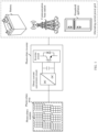
- FIG. 1 is a schematic diagram of an application scenario of a grid power supply system according to this application.
- the grid power supply system provided in this application may include a direct current power supply and a photovoltaic inverter.
- the direct current power supply may be formed by a photovoltaic array.
- An output end of the photovoltaic array may be connected to an input end of the photovoltaic inverter, and an output end of the photovoltaic inverter is connected to an alternating current power grid.
- the photovoltaic array may be formed by one or more photovoltaic strings connected in parallel, and one photovoltaic string may be obtained by connecting one or more photovoltaic modules in series.
- the photovoltaic inverter may change (step up or step down) a direct current provided by the photovoltaic array by using a direct current conversion circuit, and perform voltage inversion conversion on the direct current with a voltage transformed by using an inverter circuit to supply power to electrical equipment such as a battery, a communication base station, or a household appliance in the alternating current power grid.
- the photovoltaic inverter may include a plurality of switch transistors (which may be a metal-oxide-semiconductor field-effect transistor (MOSFET), MOS transistor for short, or may be an insulated gate bipolar transistor (insulated gate bipolar transistor, IGBT)).
- MOSFET metal-oxide-semiconductor field-effect transistor
- IGBT insulated gate bipolar transistor
- each switch transistor in the photovoltaic inverter may be turned on or turned off based on a received drive signal (for example, a pulse width modulation (Pulse Width Modulation, PWM) signal).
- PWM pulse width modulation
- the photovoltaic inverter includes a direct current conversion circuit and an inverter circuit.
- An input end of the direct current conversion circuit is configured to connect to a direct current power supply.
- An output end of the direct current conversion circuit is configured to connect to an input end of the inverter circuit.
- An output end of the inverter circuit is configured to couple to an alternating current power grid.
- the direct current conversion circuit and the inverter circuit may include a plurality of switch transistors, and the direct current conversion circuit and the inverter circuit include at least one four-pin (or 4PIN) switch transistor.
- the four-pin switch transistor may be a four-pin switch transistor having a Kelvin structure.
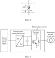
- FIG. 2 is a schematic diagram of a structure of a four-pin switch transistor.
- the four-pin switch transistor shown in FIG. 2 is a four-pin IGBT transistor, and the four-pin IGBT transistor includes an emitter E, a gate G, a collector C, and a Kelvin emitter K.
- a drive voltage may be received between the gate G and the Kelvin emitter K of the four-pin IGBT transistor (which may be a drive voltage applied by a drive unit in a photovoltaic inverter to the four-pin IGBT transistor).
- the four-pin IGBT transistor may be turned on or turned off based on the drive voltage.
- a changing power current (which may gradually increase or decrease) may be generated at the emitter E of the four-pin IGBT transistor, so that parasitic inductance Le is generated at the emitter.
- the parasitic inductance Le is separated from the drive voltage.
- the drive voltage (or the drive signal) of the four-pin IGBT transistor is separated from the power current, which avoids interference on the drive voltage by the parasitic inductance generated based on the power current of the emitter E. In this case, a build-up speed of the drive voltage between the gate and the emitter and a turn-on or turn-off speed are higher.
- a process in which a four-pin MOS transistor separates a drive voltage (or a drive signal) and a power current is similar to that of the four-pin IGBT transistor, and details are not described herein again.
- the photovoltaic inverter including the four-pin switch transistor (the four-pin IGBT transistor, the four-pin MOS transistor, and the like)
- an overall switching speed of the switch transistor is higher, and a loss of a switching cycle of the switch transistor is lower, reducing a working loss of the photovoltaic inverter. Therefore, the photovoltaic inverter has strong working reliability.
- FIG. 3 is a schematic diagram of a structure of a grid power supply system according to this application.
- the grid power supply system shown in FIG. 3 includes a direct current power supply and a photovoltaic inverter.
- the direct current power supply may be a solar panel.
- An input end of the photovoltaic inverter is coupled to the direct current power supply in the grid power supply system, and an output end of the photovoltaic inverter is connected to an alternating current power grid.
- the direct current power supply is configured to provide an energy input or a power input for the photovoltaic inverter.
- the photovoltaic inverter may change (step up or step down) a direct current provided by a photovoltaic array by using a direct current conversion circuit, and perform voltage inversion conversion on the direct current with a voltage transformed by using an inverter circuit to supply power to electrical equipment such as a battery, a communication base station, or a household appliance in the alternating current power grid.
- the four-pin switch transistor may receive the drive voltage applied by the drive unit (which may be between a gate and a Kelvin emitter or may be between a gate and a Kelvin source).
- the four-pin switch transistor may be turned on or turned off based on the drive voltage. In a turn-on or turn-off process, a changing power current (which may gradually increase or decrease) may be generated at an emitter or a source of the four-pin switch transistor, so that parasitic inductance is generated at the emitter or the source. The parasitic inductance is separated from the drive voltage.
- the direct current conversion circuit may include a plurality of direct current conversion units and output capacitors that are connected in parallel, and each direct current conversion unit in the direct current conversion circuit may include a switch transistor, an inductor, and a diode.
- FIG. 4 is a schematic diagram of a structure of a direct current conversion circuit according to this application. As shown in FIG. 4 , the direct current conversion circuit in FIG. 4 includes a plurality of direct current conversion units (which may include n direct current conversion units in total, including a direct current conversion unit 1 to a direct current conversion unit n).
- the direct current conversion circuit further includes a drive power supply and a plurality of drive units (which may include n drive units in total, including a drive unit 1 to a drive unit n, where a first input end and a second input end of each drive unit are respectively connected to a positive electrode and a negative electrode of the drive power supply).
- a switch transistor (which may be represented as a switch transistor Q1 for ease of description) in the direct current conversion unit 1 may be an IGBT transistor.
- a first end of the switch transistor Q1 (or a gate G of the switch transistor Q1) may be connected to an output end of the drive unit 1.
- a second end of the switch transistor Q1 (or an emitter E of the switch transistor Q1) is grounded.
- a third end of the switch transistor Q1 (or a collector C of the switch transistor Q1) may be connected to a direct current power supply by using an inductor (which may be represented as an inductor L1 for ease of description) in the direct current conversion unit 1.
- the third end of the switch transistor Q1 may alternatively be connected to an output capacitor (which may be represented as a capacitor Cbus for ease of description) in the direct current conversion circuit by using a diode (which may be represented as a diode D1 for ease of description) in the direct current conversion unit 1. It may be understood that a circuit structure of another direct current conversion unit in the direct current conversion circuit is the same as that of the direct current conversion unit 1, and details are not described herein again.
- a switch transistor included in at least one direct current conversion unit is a four-pin switch transistor (for example, a four-pin IGBT transistor).
- the direct current conversion unit n in FIG. 4 may be a target direct current conversion unit
- the direct current conversion unit n includes a switch transistor Qn
- the switch transistor Qn may be a four-pin switch transistor (for example, a four-pin IGBT transistor).
- a fourth end of the switch transistor Qn (or a Kelvin emitter K of the switch transistor Qn) is connected to a first end of the switch transistor Qn (or a gate G of the switch transistor Qn) and a second end of the switch transistor Qn (or an emitter E of the switch transistor Qn).
- the fourth end of the switch transistor Qn is coupled to a first input end of the drive unit n by using a capacitor C1n.
- the fourth end of the switch transistor Qn is coupled to a second input end of the drive unit n by using a capacitor C2n.
- the direct current conversion circuit may further include another target direct current conversion unit other than the direct current conversion unit n.
- a connection relationship between a four-pin switch transistor in another target direct current conversion unit and a corresponding target drive unit is the same as that in the direct current conversion unit n, and details are not described herein again.
- a drive voltage may be applied (or a drive signal may be sent) to the plurality of switch transistors in the direct current conversion circuit by using the plurality of drive units included in the direct current conversion circuit.
- the four-pin switch transistor in the target direct current conversion unit may receive a drive voltage applied by a corresponding target drive unit (which may be between a gate and a Kelvin emitter or may be between a gate and a Kelvin source).
- the drive unit n may apply a drive voltage between the first end of the switch transistor Qn (or the gate G of the switch transistor Qn) and the fourth end of the switch transistor Qn (or the Kelvin emitter K of the switch transistor Qn) based on the power supply of the drive power supply.
- the switch transistor Qn may be turned on or turned off based on the drive voltage.
- a changing power current (which may gradually increase or decrease) may be generated at the second end of the switch transistor Qn (or the emitter E of the switch transistor Qn), so that parasitic inductance is generated at the second end of the switch transistor Qn.
- the drive voltage (or the drive signal) is separated from the power current through the fourth end of the switch transistor Qn.
- a turn-on or turn-off process of a four-pin switch transistor in another target direct current conversion unit based on a drive voltage applied by a corresponding target drive unit is the same as that of the switch transistor Qn, and details are not described herein again.
- Parasitic inductance generated at the second end of the four-pin switch transistor in the direct current conversion circuit does not affect a drive voltage that is built up between the fourth end and the first end. In this case, the drive voltage is built up at a higher speed, and the four-pin switch transistor is turned on or turned off at a higher speed, increasing an overall switching speed of the switch transistor in the direct current conversion circuit.
- a switching cycle of the switch transistor has a lower loss, reducing a working loss of the direct current conversion circuit to reduce a working loss of the photovoltaic inverter. Therefore, the photovoltaic inverter has strong working reliability.
- the four-pin switch transistor included in the direct current conversion circuit in FIG. 4 may alternatively be a four-pin MOS transistor.
- a fourth end of the four-pin MOS transistor (or a Kelvin source of the switch transistor) is connected to a first end of the switch transistor (or a gate of the switch transistor) and a second end of the switch transistor (or a source of the switch transistor), and a connection relationship between the four-pin MOS transistor and another device in the direct current conversion circuit is the same as that of the four-pin IGBT transistor, and details are not described herein again.
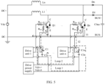
- FIG. 5 is a schematic diagram of another structure of a direct current conversion circuit according to this application.
- the direct current conversion circuit in FIG. 5 includes a plurality of direct current conversion units (which may include n direct current conversion units in total, including a direct current conversion unit 1 to a direct current conversion unit n).
- the direct current conversion circuit further includes a drive power supply and a plurality of drive units (which may include n drive units in total, including a drive unit 1 to a drive unit n, where a first input end and a second input end of each drive unit are respectively connected to a positive electrode and a negative electrode of the drive power supply).
- a switch transistor included in each direct current conversion unit in FIG. 5 is a four-pin IGBT transistor.
- the drive unit n may apply a drive voltage between a first end of a switch transistor Qn (or a gate G of the switch transistor Qn) and a fourth end of the switch transistor Qn (or a Kelvin emitter K of the switch transistor Qn) in the direct current conversion unit n based on the power supply of the drive power supply.
- the switch transistor Qn may be turned on or turned off based on the drive voltage. In a turn-on process based on the drive voltage, the switch transistor may be turned on between a second end of the switch transistor (or an emitter E of the switch transistor Qn) and a third end of the switch transistor (or a collector C of the switch transistor Qn), and the emitter E of the switch transistor Qn may output a power current 11.
- the Kelvin emitter K of the switch transistor Qn is connected to an emitter E of another switch transistor by using the drive unit n.
- the Kelvin emitter K of the switch transistor Qn can shunt and output a power current I2 (where the current is far less than the power current I1).
- the power current I2 may flow through a connection line between the drive unit n and another drive unit to an emitter E of another switch transistor other than the switch transistor Qn.
- the power current I2 outputted from the Kelvin emitter K of the switch transistor Qn flows to a switch transistor Q1 in the direct current conversion unit 1.
- the power current I2 may flow to an emitter E of the switch transistor Q1 through a loop 1 and a loop 2.
- the loop 1 includes that the power current I2 flows from the Kelvin emitter K of the switch transistor Qn to a capacitor C2n connected to the drive unit n, flows through the capacitor C2n to a capacitor C2 connected to the drive unit 1, and flows through the capacitor C2 to a Kelvin emitter K of the switch transistor Q1 to flow to the emitter E.
- the loop 2 includes that the power current I2 flows from the Kelvin emitter K of the switch transistor Qn to a capacitor C1n connected to the drive unit n, flows through the capacitor C1n to a capacitor C1 connected to the drive unit 1, and flows through the capacitor C1 to the Kelvin emitter K of the switch transistor Q1 to flow to the emitter E.
- the power current I2 shunted by the Kelvin emitter K of the switch transistor Qn flows to the emitter E of the switch transistor Q1 through a connection line between the drive unit n and the drive unit 1.
- the drive unit 1 applies a drive voltage to the switch transistor Q1 (which may be between a gate G and the Kelvin emitter K of the switch transistor Q1)
- the power current I2 affects the build-up of the drive voltage on the switch transistor Q1, which reduces a switching speed of the switch transistor Q1 and increases a switching loss of a switching cycle.
- a process in which a power current shunted by a Kelvin emitter K in any four-pin switch transistor in FIG. 5 affects a drive voltage and a switching speed of another switch transistor other than the foregoing four-pin switch transistor is the same as a process of affecting the switch transistor Qn and the switch transistor Q1, and details are not described herein again.
- each direct current conversion unit in the direct current conversion circuit shown in FIG. 4 or FIG. 5 may include an additional resistor or an additional inductor.
- a first input end and a second input end of any drive unit are coupled to a first input end and a second input end of another drive unit by using at least one additional resistor or by using at least one additional inductor.
- the direct current conversion circuit shown in FIG. 5 is used as an example for description.
- the drive unit n in FIG. 5 may be coupled to another drive unit by using the additional resistor or the additional inductor, to prevent a power current shunted and outputted by the Kelvin emitter K of the switch transistor Qn from affecting a switching speed of another switch transistor.
- FIG. 6a is a schematic diagram of another structure of a direct current conversion circuit according to this application.
- the direct current conversion circuit in FIG. 6a includes a plurality of direct current conversion units.
- a first output end of a drive unit n may be connected to a positive electrode of a drive power supply by using a resistor RZ1.
- a second output end of the drive unit n may be connected to a negative electrode of the drive power supply by using a resistor RZ2.
- impedance of a transmission line between first and second input ends of the drive unit n and first and second input ends of the drive unit 1 is much greater than impedance of a connection line between a switch transistor Qn and a switch transistor Q 1 (or a ratio of impedance of a transmission line between first and second input ends of the drive unit n and first and second input ends of the drive unit 1 to impedance of a connection line between a switch transistor Qn and a switch transistor Q1 is not less than a preset impedance ratio), so that a power current shunted and outputted by a Kelvin emitter K of the switch transistor Qn is reduced when the switch transistor Qn is turned on or turned off, thereby preventing the power current shunted and outputted by the Kelvin emitter K of the switch transistor Qn from affecting the build-up of a drive voltage of the switch transistor Q1 and a switching speed of the switch transistor Q1.
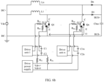
- FIG. 6b is a schematic diagram of another structure of a direct current conversion circuit according to this application.
- the direct current conversion circuit in FIG. 6b includes a plurality of direct current conversion units.
- a first output end of a drive unit 1 may be connected to a positive electrode of a drive power supply by using a resistor RZ1.
- a second output end of the drive unit 1 may be connected to a negative electrode of the drive power supply by using a resistor RZ2.
- impedance of a transmission line between first and second input ends of the drive unit n and first and second input ends of the drive unit 1 is much greater than impedance of a connection line between a switch transistor Qn and a switch transistor Q1 (or a ratio of impedance of a transmission line between first and second input ends of the drive unit n and first and second input ends of the drive unit 1 to impedance of a connection line between a switch transistor Qn and a switch transistor Q1 is not less than a preset impedance ratio), so that a power current shunted and outputted by a Kelvin emitter K of the switch transistor Qn is reduced when the switch transistor Qn is turned on or turned off, thereby preventing the power current shunted and outputted by the Kelvin emitter K of the switch transistor Qn from affecting the build-up of a drive voltage of the switch transistor Q 1 and a switching speed of the switch transistor Q1.
- impedance of a transmission line between the drive units is much greater than impedance of a connection line between the corresponding switch transistors (or a ratio of impedance of a transmission line between the drive units to impedance of a connection line between the switch transistors may be not less than a preset impedance ratio), so that a power current shunted and outputted by a Kelvin emitter or a Kelvin source is reduced when the four-pin switch transistor is turned on or turned off, thereby preventing the power current shunted and outputted by the Kelvin emitter or the Kelvin source of the four-pin switch transistor in the direct current conversion circuit from affecting the build-up of the drive voltage of the switch transistor and the switching speed of the switch transistor.
- the inverter circuit may include a plurality of inverter units, and each inverter unit may include a plurality of switch transistors.
- FIG. 7 is a schematic diagram of a structure of an inverter circuit according to this application. As shown in FIG. 7 , the inverter circuit in FIG. 7 includes three inverter units (which may include an inverter unit 1, an inverter unit 2, and an inverter unit 3). The inverter circuit further includes a drive power supply and a plurality of drive units (which may include a drive unit 1, a drive unit 2, and a drive unit 3, where a first input end and a second input end of each drive unit are respectively connected to a positive electrode and a negative electrode of the drive power supply).
- An output end of any drive unit is connected to a first end of a switch transistor (which may be a target switch transistor) in a plurality of switch transistors of an inverter unit associated with the any drive unit.
- a target switch transistor included in at least one of the plurality of inverter units is a four-pin switch transistor. This application uses an example in which target switch transistors included in the plurality of inverter units are all four-pin switch transistors for description.
- the inverter circuit further includes a first direct current capacitor (which may be represented as a capacitor Cbus_n for ease of description) and a second direct current capacitor (which may be represented as a capacitor Cbus_p for ease of description) that are connected in series. Refer to FIG. 7 again.
- a target switch transistor (which may be represented as a switch transistor Q4_A for ease of description) connected to the drive unit 1 associated with the inverter unit 1 may be a four-pin IGBT transistor.
- An output end of the drive unit 1 is connected to a first end of the switch transistor Q4_A (or a gate G of the switch transistor Q4_A).
- a second end of the switch transistor Q4_A (or an emitter E of the switch transistor Q4_A) is connected to the capacitor Cbus_n.
- a third end of the switch transistor Q4_A (or a collector C of the switch transistor Q4_A) is connected to the second direct current capacitor by using a switch transistor (which may be represented as a switch transistor Q 1_A for ease of description) in the inverter unit 1, and is connected to connection ends of the capacitor Cbus_n and the capacitor Cbus_p by using two switch transistors (which may be respectively represented as a switch transistor Q2_A and a switch transistor Q3_A for ease of description) connected in series in the inverter unit 1.
- a fourth end of the switch transistor Q4_A (or a Kelvin emitter K of the switch transistor Q4_A) is connected to the first end and the second end of the switch transistor.
- the fourth end of the switch transistor Q4_A is coupled to a first input end and a second input end of the drive unit 1. It may be understood that a circuit structure of another inverter unit in the inverter circuit is the same as that of the inverter unit 1, and details are not described herein again.
- a drive voltage may be applied (or a drive signal may be sent) to the plurality of switch transistors in the inverter circuit by using the plurality of drive units included in the inverter circuit.
- the four-pin switch transistor in the inverter unit may receive a drive voltage applied by a corresponding drive unit (which may be between a gate and a Kelvin emitter or may be between a gate and a Kelvin source).
- the drive unit 1 may apply a drive voltage between the first end of the switch transistor Q4_A (or the gate G of the switch transistor Q4_A) and the fourth end of the switch transistor Q4_A (or the Kelvin emitter K of the switch transistor Q4_A) based on the power supply of the drive power supply.
- the switch transistor Q4_A may be turned on or turned off based on the drive voltage.
- a changing power current (which may gradually increase or decrease) may be generated at the second end of the switch transistor Q4_A (or the emitter E of the switch transistor Q4_A), so that parasitic inductance is generated at the second end of the switch transistor Q4_A.
- the photovoltaic inverter has strong working reliability.
- the four-pin switch transistor included in the direct current conversion circuit in FIG. 7 may alternatively be a four-pin MOS transistor.
- a fourth end of the four-pin MOS transistor (or a Kelvin source of the switch transistor) is connected to a first end of the switch transistor (or a gate of the switch transistor) and a second end of the switch transistor (or a source of the switch transistor), and a connection relationship between the four-pin MOS transistor and another device in the direct current conversion circuit is the same as that of the four-pin IGBT transistor, and details are not described herein again.
- the switch transistor Q4_C in a process in which a four-pin switch transistor, for example, a switch transistor Q4_C, in the inverter circuit shown in FIG. 7 is turned on or turned off based on a drive voltage, the switch transistor Q4_C may be turned on between a second end of the switch transistor Q4_C (or an emitter E of the switch transistor Q4_C) and a third end of the switch transistor Q4_C (or a collector C of the switch transistor Q4_C), and the emitter E of the switch transistor Q4_C may output a power current I1.
- the loop 2 includes that the power current I2 flows from the Kelvin emitter K of the switch transistor Q4_C to a capacitor C1c connected to the drive unit 3, flows through the capacitor C1c to a capacitor C1b connected to the drive unit 2, and flows through the capacitor C1b to the Kelvin emitter K of the switch transistor Q4_B to flow to the emitter E.
- the power current I2 shunted by the Kelvin emitter K of the switch transistor Q4_C flows to the emitter E of the switch transistor Q4_B through a connection line between the drive unit 3 and the drive unit 2.
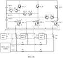
- FIG. 8a is a schematic diagram of another structure of an inverter circuit according to this application.
- the inverter circuit in FIG. 8a includes three inverter units.
- a first output end and a second output end of a drive unit 1 may be respectively connected to a positive electrode and a negative electrode of a drive power supply by using a resistor RZ_a1 and a resistor RZ_a2.
- a first output end and a second output end of a drive unit 2 may be respectively connected to the positive electrode and the negative electrode of the drive power supply by using a resistor RZ_b1 and a resistor RZ_b2.
- a first output end and a second output end of a drive unit 3 may be respectively connected to the positive electrode and the negative electrode of the drive power supply by using a resistor RZ_c1 and a resistor RZ_c2.
- impedance of transmission lines between first and second input ends of the drive unit 3 and first and second input ends of the drive unit 1 and between the first and second input ends of the drive unit 3 and first and second input ends of the drive unit 2 is much greater than impedance of connection lines between the switch transistor Q4_C and the switch transistor Q4_A and between the switch transistor Q4_C and the switch transistor Q4_B (or a ratio of the impedance of the transmission line between the first and second input ends of the drive unit 3 and the first and second input ends of the drive unit 1 (or the drive unit 2) to the impedance of the connection line between the switch transistor Q4_C and the switch transistor Q4_A is not less
- FIG. 8b is a schematic diagram of another structure of an inverter circuit according to this application.
- the inverter circuit in FIG. 8b includes three inverter units.
- a first output end and a second output end of a drive unit 1 may be respectively connected to a first output end and a second output end of a drive unit 2 by using resistors RZ1 and RZ2.
- the first output end and the second output end of the drive unit 2 may be respectively connected to a first output end and a second output end of a drive unit 3 by using resistors RZ3 and RZ4.
- impedance of transmission lines between first and second input ends of the drive unit 3 and first and second input ends of the drive unit 1 and between the first and second input ends of the drive unit 3 and first and second input ends of the drive unit 2 is much greater than impedance of connection lines between the switch transistor Q4_C and the switch transistor Q4_A and between the switch transistor Q4_C and the switch transistor Q4_B (or a ratio of the impedance of the transmission line between the first and second input ends of the drive unit 3 and the first and second input ends of the drive unit 1 (or the drive unit 2) to the impedance of the connection line between the switch transistor Q4_C and the switch transistor Q4_A is not less than a preset impedance ratio), so that a power current shunted and outputted by the Kelvin emitter K of the switch transistor Q4_C when the switch transistor Q4_C is turned on or turned off, thereby
- the drive unit 3 may be coupled to another drive unit by using an additional inductor to increase impedance of the transmission line.
- a resistor or an inductor may be formed between the drive unit 3 and another drive unit by PCB wiring to increase the impedance of the transmission line. This may be specifically determined according to an actual application scenario, and is not limited herein.
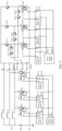
- FIG. 9 is a schematic diagram of a structure of a photovoltaic inverter according to this application.
- the photovoltaic inverter in FIG. 9 includes a direct current conversion circuit and an inverter circuit.
- the direct current conversion circuit includes a plurality of direct current conversion units (which may include n direct current conversion units in total, including a direct current conversion unit 1 to a direct current conversion unit n).
- the direct current conversion circuit further includes a drive power supply and a plurality of drive units (which may include n drive units in total, including a drive unit 1 to a drive unit n, where a first input end and a second input end of each drive unit are respectively connected to a positive electrode and a negative electrode of the drive power supply).
- the direct current conversion units in FIG. 9 are the same as the direct current conversion units included in the direct current conversion circuit in FIG. 5 , and details are not described herein again.
- the inverter circuit includes three inverter units (which may include an inverter unit 1, an inverter unit 2, and an inverter unit 3).
- the inverter circuit further includes a drive power supply and a plurality of drive units (which may include a drive unit a, a drive unit b, and a drive unit c, where a first input end and a second input end of each drive unit are respectively connected to a positive electrode and a negative electrode of the drive power supply).
- the inverter units in FIG. 9 are the same as the inverter units included in the inverter circuit in FIG. 7 , and details are not described herein again.
- a target switch transistor included in at least one inverter unit in the plurality of inverter units is a four-pin switch transistor.
- a fourth end of the four-pin switch transistor is connected to a first end and a second end of the four-pin switch transistor.
- the fourth end of the four-pin switch transistor is coupled to a first input end and a second input end of a target drive unit connected to the at least one direct current conversion unit or the at least one inverter unit.
- the photovoltaic inverter may be configured to separate, through the fourth end of the four-pin switch transistor, a power current outputted from the second end of the four-pin switch transistor and a drive voltage applied by the target drive unit, to avoid interference on the drive voltage caused by parasitic inductance generated based on the power current.
- each direct current conversion unit in the direct current conversion circuit and each inverter unit in the inverter circuit that are shown in FIG. 9 may include an additional resistor or an additional inductor.
- each direct current conversion unit and the additional resistor or the additional inductor refer to the direct current conversion circuits shown in FIG. 6a and FIG. 6b .
- each inverter unit and the additional resistor or the additional inductor refer to the inverter circuits shown in FIG. 8a and FIG. 8b .
- impedance of a transmission line between the drive units is much greater than impedance of a connection line between the corresponding switch transistors (or a ratio of impedance of a transmission line between the drive units to impedance of a connection line between the switch transistors may be not less than a preset impedance ratio), so that a power current shunted and outputted by a Kelvin emitter or a Kelvin source is reduced when the four-pin switch transistor in the photovoltaic inverter is turned on or turned off, thereby preventing the power current shunted and outputted by the Kelvin emitter or the Kelvin source of the four-pin switch transistor in the photovoltaic inverter from affecting the build-up of the drive voltage of the switch transistor and the switching speed of the switch transistor.
- the photovoltaic inverter includes a direct current conversion circuit and an inverter circuit.
- An input end of the direct current conversion circuit is configured to connect to a direct current power supply.
- An output end of the direct current conversion circuit is configured to connect to an input end of the inverter circuit.
- An output end of the inverter circuit is configured to couple to an alternating current power grid.
- the direct current conversion circuit and the inverter circuit may include a plurality of switch transistors, and the direct current conversion circuit and the inverter circuit include at least one four-pin (or 4PIN) switch transistor.
- the four-pin switch transistor may be a four-pin switch transistor having a Kelvin structure.
- a drive voltage may be received between a first end and a fourth end of the four-pin switch transistor (which may be a drive voltage applied by a drive unit in the photovoltaic inverter to the four-pin switch transistor).
- the four-pin switch transistor may be turned on or turned off based on the drive voltage. In a turn-on or turn-off process, a changing power current (which may gradually increase or decrease) may be generated at a second end of the four-pin switch transistor, so that parasitic inductance is generated at an emitter.
- the four-pin switch transistor may separate the parasitic inductance from the drive voltage through the fourth end (a Kelvin emitter or a Kelvin source).
- the drive voltage (or the drive signal) of the four-pin switch transistor is separated from the power current, which avoids interference on the drive voltage by the parasitic inductance generated based on the power current.
- a build-up speed of the drive voltage and a turn-on or turn-off speed are higher, and a loss of an overall switching cycle of the switch transistor in the photovoltaic inverter is lower.
- the direct current conversion circuit and the inverter circuit in the photovoltaic inverter may further include an additional resistor or an additional inductor.
- impedance of a transmission line between the drive units in the direct current conversion circuit and in the inverter circuit is much greater than impedance of a connection line between the corresponding switch transistors (or a ratio of impedance of a transmission line between the drive units to impedance of a connection line between the switch transistors may be not less than a preset impedance ratio), so that a power current shunted and outputted by the Kelvin emitter or the Kelvin source is reduced when the four-pin switch transistor in the direct current conversion circuit and the inverter circuit is turned on or turned off, which prevents the power current shunted and outputted by the Kelvin emitter or the Kelvin source of the four-pin switch transistor in the photovoltaic inverter from affecting the build-up of the drive voltage of the switch transistor and the switching speed of the switch transistor, reducing a working loss of the photovoltaic inverter. Therefore, the photovoltaic inverter has strong working reliability.
Landscapes
- Engineering & Computer Science (AREA)
- Power Engineering (AREA)
- Inverter Devices (AREA)
- Power Conversion In General (AREA)
Abstract
Description
- This application relates to the field of power electronics, and in particular, to a photovoltaic inverter, a direct current conversion circuit, and an inverter circuit.
- For power supply equipment (such as a switching power supply and an inverter), efficiency and thermal design are important aspects in design of the power supply equipment. Power devices (such as various switch transistors and transistors) are key components in the power supply equipment. Loss reduction of the power devices plays a key role in the efficiency and thermal design of the power supply equipment. So far, most switch transistors and transistors are three-pin (or 3PIN) devices with a drive part compared with diodes. For a three-pin device, interaction between a power loop and a drive voltage signal is more sensitive. For example, in each switching cycle (on or off), stray inductance of a source or an emitter of a switch transistor plus switch current slope generates a voltage signal opposite to a drive voltage signal of a transistor, which reduces a switching speed of the switch transistor and increases a switching loss of each switching cycle, resulting in an increase in heat consumption of power supply equipment. Therefore, how to resolve a problem of an increase of a working loss of the power supply equipment due to reduction of the switching speed of the switch transistor caused by interaction between the power loop and the drive voltage signal of the switch transistor and the transistor in the power supply equipment is one of the technical problems that need to be urgently resolved currently.
- Embodiments of this application provide a photovoltaic inverter, a direct current conversion circuit, and an inverter circuit, to avoid interference on a drive voltage by parasitic inductance generated based on a power current of a switch transistor, thereby increasing an overall switching speed of the switch transistor in the photovoltaic inverter, and reducing a working loss of the photovoltaic inverter.
- According to a first aspect, this application provides a photovoltaic inverter. The photovoltaic inverter includes a direct current conversion circuit and an inverter circuit. An input end of the direct current conversion circuit is configured to connect to a direct current power supply. An output end of the direct current conversion circuit is configured to connect to an input end of the inverter circuit. An output end of the inverter circuit is configured to couple to an alternating current power grid. The direct current conversion circuit includes a plurality of direct current conversion units connected in parallel. The inverter circuit includes a plurality of inverter units. The photovoltaic inverter further includes a drive power supply and a plurality of drive units. A first input end and a second input end of each drive unit are respectively connected to a positive electrode and a negative electrode of the drive power supply. Each direct current conversion unit and each inverter unit further include a switch transistor. An output end of any drive unit is connected to a first end of one switch transistor in the direct current conversion unit or is connected to a first end of one target switch transistor in a plurality of switch transistors of an inverter unit associated with the any drive unit. At least one of the plurality of direct current conversion units includes a four-pin switch transistor or a target switch transistor included in at least one of the plurality of inverter units is a four-pin switch transistor. A fourth end of the four-pin switch transistor is connected to a first end and a second end of the four-pin switch transistor. The fourth end of the four-pin switch transistor is coupled to a first input end and a second input end of a target drive unit connected to the at least one direct current conversion unit or the at least one inverter unit. The photovoltaic inverter is configured to separate, through the fourth end of the four-pin switch transistor, a power current outputted from the second end of the four-pin switch transistor and a drive voltage applied by the target drive unit, to avoid interference on the drive voltage caused by parasitic inductance generated based on the power current.
- In this application, parasitic inductance generated at the second end of the four-pin switch transistor in the direct current conversion circuit or the inverter circuit in the photovoltaic inverter does not affect a drive voltage that is built up between the fourth end and the first end. In this case, the drive voltage is built up at a higher speed, and the four-pin switch transistor is turned on or turned off at a higher speed, increasing an overall switching speed of the switch transistor in the direct current conversion circuit. In addition, a switching cycle of the switch transistor has a lower loss, reducing a working loss of the direct current conversion circuit or the inverter circuit to reduce a working loss of the photovoltaic inverter. Therefore, the photovoltaic inverter has strong working reliability.
- With reference to the first aspect, in a first possible implementation, the direct current conversion circuit further includes an output capacitor, each direct current conversion unit further includes an inductor and a diode, a second end of a switch transistor in each direct current conversion unit is grounded, and a third end of the switch transistor in each direct current conversion unit is connected to the direct current power supply by using the inductor and is connected to the output capacitor by using the diode. Herein, parasitic inductance generated at the second end of the four-pin switch transistor in the direct current conversion circuit does not affect a drive voltage that is built up between the fourth end and the first end. In this case, the drive voltage is built up at a higher speed, and the four-pin switch transistor is turned on or turned off at a higher speed, increasing an overall switching speed of the switch transistor in the direct current conversion circuit. In addition, a switching cycle of the switch transistor has a lower loss.
- With reference to the first aspect, in a second possible implementation, the inverter circuit further includes a first direct current capacitor and a second direct current capacitor that are connected in series, a second end of a four-pin switch transistor in any inverter unit is connected to the first direct current capacitor, and a third end of the four-pin switch transistor in the any inverter unit is connected to the second direct current capacitor by using one switch transistor in the any inverter unit and is connected to connection ends of the first direct current capacitor and the second direct current capacitor by using two switch transistors connected in series in the any inverter unit. Herein, parasitic inductance generated at the second end of the four-pin switch transistor in the inverter circuit does not affect a drive voltage that is built up between the fourth end and the first end. In this case, the drive voltage is built up at a higher speed, and the four-pin switch transistor is turned on or turned off at a higher speed, increasing an overall switching speed of the switch transistor in the inverter circuit. In addition, a switching cycle of the switch transistor has a lower loss.
- With reference to any one of the first aspect to the second possible implementation of the first aspect, in a third possible implementation, each direct current conversion unit and each inverter unit further include an additional resistor or an additional inductor, and a first input end and a second input end of the any drive unit are coupled to a first input end and a second input end of another drive unit by using at least one additional resistor or additional inductor. By adding the additional resistor or the additional inductor, impedance of a transmission line between the drive units is much greater than impedance of a connection line between the corresponding switch transistors (or a ratio of impedance of a transmission line between the drive units to impedance of a connection line between the switch transistors may be not less than a preset impedance ratio), so that a power current shunted and outputted by a Kelvin emitter or a Kelvin source is reduced when the four-pin switch transistor is turned on or turned off, thereby preventing the power current shunted and outputted by the Kelvin emitter or the Kelvin source of the four-pin switch transistor in the direct current conversion circuit or the inverter circuit from affecting the build-up of the drive voltage of the switch transistor and the switching speed of the switch transistor.
- With reference to the third possible implementation of the first aspect, in a fourth possible implementation, the switch transistor and the four-pin switch transistor are IGBTs; the first ends of the switch transistor and the four-pin switch transistor are gates, the second ends are emitters, and the third ends are collectors; and the fourth end of the four-pin switch transistor is connected to the emitter and the gate of the four-pin switch transistor; or the switch transistor and the four-pin switch transistor are MOS transistors; the first ends of the switch transistor and the four-pin switch transistor are gates, the second ends are sources, and the third ends are drains; and the fourth end of the four-pin switch transistor is connected to the source and the gate of the four-pin switch transistor. A drive voltage (or a drive signal) of the four-pin switch transistor is separated from a power current, which avoids interference on the drive voltage by parasitic inductance generated based on a power current of the emitter or the source. In this case, a build-up speed of the drive voltage and a turn-on or turn-off speed are higher, increasing an overall switching speed of the switch transistor in the photovoltaic inverter. In addition, a switching cycle of the switch transistor has a lower loss.
- According to a second aspect, this application provides a direct current conversion circuit. The direct current conversion circuit includes a plurality of direct current conversion units connected in parallel, an output capacitor, a drive power supply, and a plurality of drive units. Each direct current conversion unit includes a switch transistor, an inductor, and a diode. A first input end and a second input end of each drive unit are respectively connected to a positive electrode and a negative electrode of the drive power supply. An output end of one drive unit is connected to a first end of a switch transistor in one direct current conversion unit. A second end of the switch transistor is grounded. A third end of the switch transistor is connected to a direct current power supply by using the inductor and is connected to the output capacitor by using the diode. A switch transistor included in at least one of the plurality of direct current conversion units is a four-pin switch transistor. A fourth end of the four-pin switch transistor is connected to a first end and a second end of the four-pin switch transistor. The fourth end of the four-pin switch transistor is coupled to a first input end and a second input end of a target drive unit connected to the at least one direct current conversion unit. The fourth end of the four-pin switch transistor is configured to separate a power current outputted from the second end of the four-pin switch transistor and a drive voltage applied by the target drive unit, to avoid interference on the drive voltage caused by parasitic inductance generated based on the power current.
- In this application, parasitic inductance generated at the second end of the four-pin switch transistor in the direct current conversion circuit does not affect a drive voltage that is built up between the fourth end and the first end. In this case, the drive voltage is built up at a higher speed, and the four-pin switch transistor is turned on or turned off at a higher speed, increasing an overall switching speed of the switch transistor in the direct current conversion circuit. In addition, a switching cycle of the switch transistor has a lower loss, reducing a working loss of the direct current conversion circuit to reduce a working loss of the photovoltaic inverter. Therefore, the photovoltaic inverter has strong working reliability.
- With reference to the second aspect, in a first possible implementation, each direct current conversion unit further includes an additional resistor or an additional inductor, and a first input end and a second input end of any drive unit are coupled to a first input end and a second input end of another drive unit by using at least one additional resistor or additional inductor. By adding the additional resistor or the additional inductor, impedance of a transmission line between the drive units is much greater than impedance of a connection line between the corresponding switch transistors (or a ratio of impedance of a transmission line between the drive units to impedance of a connection line between the switch transistors may be not less than a preset impedance ratio), so that a power current shunted and outputted by a Kelvin emitter or a Kelvin source is reduced when the four-pin switch transistor is turned on or turned off, thereby preventing the power current shunted and outputted by the Kelvin emitter or the Kelvin source of the four-pin switch transistor in the direct current conversion circuit from affecting the build-up of the drive voltage of the switch transistor and the switching speed of the switch transistor.
- With reference to the first possible implementation of the second aspect, in a second possible implementation, the switch transistor and the four-pin switch transistor are IGBTs; the first ends of the switch transistor and the four-pin switch transistor are gates, the second ends are emitters, and the third ends are collectors; and the fourth end of the four-pin switch transistor is connected to the emitter and the gate of the four-pin switch transistor; or the switch transistor and the four-pin switch transistor are MOS transistors; the first ends of the switch transistor and the four-pin switch transistor are gates, the second ends are sources, and the third ends are drains; and the fourth end of the four-pin switch transistor is connected to the source and the gate of the four-pin switch transistor. A drive voltage (or a drive signal) of the four-pin switch transistor is separated from a power current, which avoids interference on the drive voltage by parasitic inductance generated based on a power current of the emitter or the source. In this case, a build-up speed of the drive voltage and a turn-on or turn-off speed are higher, increasing an overall switching speed of the switch transistor in the photovoltaic inverter. In addition, a switching cycle of the switch transistor has a lower loss.
- According to a third aspect, this application provides an inverter circuit. The inverter circuit includes a plurality of inverter units, a drive power supply, and a plurality of drive units. Each inverter unit includes a plurality of switch transistors. A first input end and a second input end of each drive unit are respectively connected to a positive electrode and a negative electrode of the drive power supply. An output end of any drive unit is connected to a first end of a target switch transistor in a plurality of switch transistors of an inverter unit associated with the any drive unit. The inverter circuit further includes a first direct current capacitor and a second direct current capacitor that are connected in series. A second end of a target switch transistor in any inverter unit is connected to the first direct current capacitor. A third end of the target switch transistor in the any inverter unit is connected to the second direct current capacitor by using one switch transistor in the any inverter unit and is connected to connection ends of the first direct current capacitor and the second direct current capacitor by using two switch transistors connected in series in the any inverter unit. A target switch transistor included in at least one of the plurality of inverter units is a four-pin switch transistor.
- A fourth end of the four-pin switch transistor is connected to a first end and a second end of the four-pin switch transistor. The fourth end of the four-pin switch transistor is coupled to a first input end and a second input end of a target drive unit connected to the at least one inverter unit. The fourth end of the four-pin switch transistor is configured to separate a power current outputted from the second end of the four-pin switch transistor and a drive voltage applied by the target drive unit, to avoid interference on the drive voltage caused by parasitic inductance generated based on the power current.
- In this application, parasitic inductance generated at the second end of the four-pin switch transistor in the inverter circuit does not affect a drive voltage that is built up between the fourth end and the first end. In this case, the drive voltage is built up at a higher speed, and the four-pin switch transistor is turned on or turned off at a higher speed, increasing an overall switching speed of the switch transistor in the inverter circuit. In addition, a switching cycle of the switch transistor has a lower loss, reducing a working loss of the inverter circuit to reduce a working loss of the photovoltaic inverter. Therefore, the photovoltaic inverter has strong working reliability.
- With reference to the third aspect, in a first possible implementation, each inverter unit further includes an additional resistor or an additional inductor, and a first input end and a second input end of the any drive unit are coupled to a first input end and a second input end of another drive unit by using at least one additional resistor or additional inductor. By adding the additional resistor or the additional inductor, impedance of a transmission line between the drive units is much greater than impedance of a connection line between the corresponding switch transistors (or a ratio of impedance of a transmission line between the drive units to impedance of a connection line between the switch transistors may be not less than a preset impedance ratio), so that a power current shunted and outputted by a Kelvin emitter or a Kelvin source is reduced when the four-pin switch transistor is turned on or turned off, thereby preventing the power current shunted and outputted by the Kelvin emitter or the Kelvin source of the four-pin switch transistor in the inverter circuit from affecting the build-up of the drive voltage of the switch transistor and the switching speed of the switch transistor.
- With reference to the first possible implementation of the third aspect, in a second possible implementation, the switch transistor and the four-pin switch transistor are IGBTs; the first ends of the switch transistor and the four-pin switch transistor are gates, the second ends are emitters, and the third ends are collectors; and the fourth end of the four-pin switch transistor is connected to the emitter and the gate of the four-pin switch transistor; or the switch transistor and the four-pin switch transistor are MOS transistors; the first ends of the switch transistor and the four-pin switch transistor are gates, the second ends are sources, and the third ends are drains; and the fourth end of the four-pin switch transistor is connected to the source and the gate of the four-pin switch transistor. A drive voltage (or a drive signal) of the four-pin switch transistor is separated from a power current, which avoids interference on the drive voltage by parasitic inductance generated based on a power current of the emitter or the source. In this case, a build-up speed of the drive voltage and a turn-on or turn-off speed are higher, increasing an overall switching speed of the switch transistor in the photovoltaic inverter. In addition, a switching cycle of the switch transistor has a lower loss.
-
-
FIG. 1 is a schematic diagram of an application scenario of a grid power supply system according to this application; -
FIG. 2 is a schematic diagram of a structure of a four-pin switch transistor; -
FIG. 3 is a schematic diagram of a structure of a grid power supply system according to this application; -
FIG. 4 is a schematic diagram of a structure of a direct current conversion circuit according to this application; -
FIG. 5 is a schematic diagram of another structure of a direct current conversion circuit according to this application; -
FIG. 6a is a schematic diagram of another structure of a direct current conversion circuit according to this application; -
FIG. 6b is a schematic diagram of another structure of a direct current conversion circuit according to this application; -
FIG. 7 is a schematic diagram of a structure of an inverter circuit according to this application; -
FIG. 8a is a schematic diagram of another structure of an inverter circuit according to this application; -
FIG. 8b is a schematic diagram of another structure of an inverter circuit according to this application; and -
FIG. 9 is a schematic diagram of a structure of a photovoltaic inverter according to this application -
FIG. 1 is a schematic diagram of an application scenario of a grid power supply system according to this application. The grid power supply system provided in this application may include a direct current power supply and a photovoltaic inverter. The direct current power supply may be formed by a photovoltaic array. An output end of the photovoltaic array may be connected to an input end of the photovoltaic inverter, and an output end of the photovoltaic inverter is connected to an alternating current power grid. In the grid power supply system shown inFIG. 1 , the photovoltaic array may be formed by one or more photovoltaic strings connected in parallel, and one photovoltaic string may be obtained by connecting one or more photovoltaic modules in series. The photovoltaic inverter may change (step up or step down) a direct current provided by the photovoltaic array by using a direct current conversion circuit, and perform voltage inversion conversion on the direct current with a voltage transformed by using an inverter circuit to supply power to electrical equipment such as a battery, a communication base station, or a household appliance in the alternating current power grid. - In the application scenario shown in
FIG. 1 , when the grid power supply system supplies power to the alternating current power grid, the photovoltaic inverter may include a plurality of switch transistors (which may be a metal-oxide-semiconductor field-effect transistor (MOSFET), MOS transistor for short, or may be an insulated gate bipolar transistor (insulated gate bipolar transistor, IGBT)). In a working process of the photovoltaic inverter of the grid power supply system, each switch transistor in the photovoltaic inverter may be turned on or turned off based on a received drive signal (for example, a pulse width modulation (Pulse Width Modulation, PWM) signal). Herein, most switch transistors in the photovoltaic inverter are three-pin (or 3PIN) devices with a drive part compared with diodes. For a three-pin device, there is an interaction problem between a power loop and a drive voltage signal. For example, using an IGBT transistor including three pins as an example, in each switching cycle (on or off) of the switch transistor, because parasitic inductance (or stray inductance) is generated at an emitter of the switch transistor due to change of a current (or change of a power current of a power loop) on the emitter of the switch transistor, and the parasitic inductance of the emitter of the switch transistor plus switch current slope generates a voltage signal opposite to a drive voltage signal, the build-up of a drive voltage between a gate and the emitter of the switch transistor is affected, consequently reducing a switching speed of the switch transistor and increasing a switching loss of each switching cycle. In a turn-on or turn-off process of each IGBT transistor or MOS transistor that includes three pins in the photovoltaic inverter, an overall switching speed of the switch transistor is reduced due to the interaction between the power loop and the drive voltage signal, which increases a working loss of the photovoltaic inverter. Consequently, the photovoltaic inverter has low working reliability. - In the grid power supply system provided in this application, the photovoltaic inverter includes a direct current conversion circuit and an inverter circuit. An input end of the direct current conversion circuit is configured to connect to a direct current power supply. An output end of the direct current conversion circuit is configured to connect to an input end of the inverter circuit. An output end of the inverter circuit is configured to couple to an alternating current power grid. The direct current conversion circuit and the inverter circuit may include a plurality of switch transistors, and the direct current conversion circuit and the inverter circuit include at least one four-pin (or 4PIN) switch transistor. The four-pin switch transistor may be a four-pin switch transistor having a Kelvin structure.
FIG. 2 is a schematic diagram of a structure of a four-pin switch transistor. The four-pin switch transistor shown inFIG. 2 is a four-pin IGBT transistor, and the four-pin IGBT transistor includes an emitter E, a gate G, a collector C, and a Kelvin emitter K. A drive voltage may be received between the gate G and the Kelvin emitter K of the four-pin IGBT transistor (which may be a drive voltage applied by a drive unit in a photovoltaic inverter to the four-pin IGBT transistor). The four-pin IGBT transistor may be turned on or turned off based on the drive voltage. In a turn-on or turn-off process, a changing power current (which may gradually increase or decrease) may be generated at the emitter E of the four-pin IGBT transistor, so that parasitic inductance Le is generated at the emitter. The parasitic inductance Le is separated from the drive voltage. The drive voltage (or the drive signal) of the four-pin IGBT transistor is separated from the power current, which avoids interference on the drive voltage by the parasitic inductance generated based on the power current of the emitter E. In this case, a build-up speed of the drive voltage between the gate and the emitter and a turn-on or turn-off speed are higher. Similarly, a process in which a four-pin MOS transistor separates a drive voltage (or a drive signal) and a power current is similar to that of the four-pin IGBT transistor, and details are not described herein again. In the photovoltaic inverter including the four-pin switch transistor (the four-pin IGBT transistor, the four-pin MOS transistor, and the like), an overall switching speed of the switch transistor is higher, and a loss of a switching cycle of the switch transistor is lower, reducing a working loss of the photovoltaic inverter. Therefore, the photovoltaic inverter has strong working reliability. -
FIG. 3 is a schematic diagram of a structure of a grid power supply system according to this application. The grid power supply system shown inFIG. 3 includes a direct current power supply and a photovoltaic inverter. The direct current power supply may be a solar panel. An input end of the photovoltaic inverter is coupled to the direct current power supply in the grid power supply system, and an output end of the photovoltaic inverter is connected to an alternating current power grid. In the grid power supply system shown inFIG. 3 , the direct current power supply is configured to provide an energy input or a power input for the photovoltaic inverter. The photovoltaic inverter may change (step up or step down) a direct current provided by a photovoltaic array by using a direct current conversion circuit, and perform voltage inversion conversion on the direct current with a voltage transformed by using an inverter circuit to supply power to electrical equipment such as a battery, a communication base station, or a household appliance in the alternating current power grid. - In some feasible implementations, in the grid power supply system shown in
FIG. 3 , the direct current conversion circuit and the inverter circuit in the photovoltaic inverter may include a plurality of switch transistors, and the direct current conversion circuit and the inverter circuit may include at least one four-pin (or 4PIN) switch transistor. The four-pin switch transistor may be a four-pin switch transistor (a four-pin IGBT transistor, a four-pin MOS transistor, or the like) having a Kelvin structure. In a working process of the photovoltaic inverter, a drive voltage may be applied (or a drive signal may be sent) to the plurality of switch transistors in the direct current conversion circuit and the inverter circuit by using a drive unit (which is not shown inFIG. 3 and may be based on the power supply of a drive power supply). The four-pin switch transistor (the four-pin IGBT transistor, the four-pin MOS transistor, or the like) may receive the drive voltage applied by the drive unit (which may be between a gate and a Kelvin emitter or may be between a gate and a Kelvin source). The four-pin switch transistor may be turned on or turned off based on the drive voltage. In a turn-on or turn-off process, a changing power current (which may gradually increase or decrease) may be generated at an emitter or a source of the four-pin switch transistor, so that parasitic inductance is generated at the emitter or the source. The parasitic inductance is separated from the drive voltage. The drive voltage (or the drive signal) of the four-pin switch transistor is separated from the power current, which avoids interference on the drive voltage by the parasitic inductance generated based on the power current of the emitter or the source. In this case, a build-up speed of the drive voltage and a turn-on or turn-off speed are higher, increasing an overall switching speed of the switch transistor in the photovoltaic inverter. In addition, a switching cycle of the switch transistor has a lower loss, reducing a working loss of the photovoltaic inverter. Therefore, the photovoltaic inverter has strong working reliability. - The following describes, with reference to
FIG. 4 to FIG. 9 , examples of a direct current conversion circuit and an inverter circuit provided in embodiments of this application. In some feasible implementations, the direct current conversion circuit may include a plurality of direct current conversion units and output capacitors that are connected in parallel, and each direct current conversion unit in the direct current conversion circuit may include a switch transistor, an inductor, and a diode.FIG. 4 is a schematic diagram of a structure of a direct current conversion circuit according to this application. As shown inFIG. 4 , the direct current conversion circuit inFIG. 4 includes a plurality of direct current conversion units (which may include n direct current conversion units in total, including a directcurrent conversion unit 1 to a direct current conversion unit n). The direct current conversion circuit further includes a drive power supply and a plurality of drive units (which may include n drive units in total, including adrive unit 1 to a drive unit n, where a first input end and a second input end of each drive unit are respectively connected to a positive electrode and a negative electrode of the drive power supply). A switch transistor (which may be represented as a switch transistor Q1 for ease of description) in the directcurrent conversion unit 1 may be an IGBT transistor. A first end of the switch transistor Q1 (or a gate G of the switch transistor Q1) may be connected to an output end of thedrive unit 1. A second end of the switch transistor Q1 (or an emitter E of the switch transistor Q1) is grounded. A third end of the switch transistor Q1 (or a collector C of the switch transistor Q1) may be connected to a direct current power supply by using an inductor (which may be represented as an inductor L1 for ease of description) in the directcurrent conversion unit 1. The third end of the switch transistor Q1 may alternatively be connected to an output capacitor (which may be represented as a capacitor Cbus for ease of description) in the direct current conversion circuit by using a diode (which may be represented as a diode D1 for ease of description) in the directcurrent conversion unit 1. It may be understood that a circuit structure of another direct current conversion unit in the direct current conversion circuit is the same as that of the directcurrent conversion unit 1, and details are not described herein again. - In some feasible implementations, in the plurality of direct current conversion units of the direct current conversion circuit shown in
FIG. 4 , a switch transistor included in at least one direct current conversion unit (which may be a target direct current conversion unit) is a four-pin switch transistor (for example, a four-pin IGBT transistor). Refer toFIG. 4 again. The direct current conversion unit n inFIG. 4 may be a target direct current conversion unit, the direct current conversion unit n includes a switch transistor Qn, and the switch transistor Qn may be a four-pin switch transistor (for example, a four-pin IGBT transistor). A fourth end of the switch transistor Qn (or a Kelvin emitter K of the switch transistor Qn) is connected to a first end of the switch transistor Qn (or a gate G of the switch transistor Qn) and a second end of the switch transistor Qn (or an emitter E of the switch transistor Qn). The fourth end of the switch transistor Qn is coupled to a first input end of the drive unit n by using a capacitor C1n. The fourth end of the switch transistor Qn is coupled to a second input end of the drive unit n by using a capacitor C2n. It may be understood that the direct current conversion circuit may further include another target direct current conversion unit other than the direct current conversion unit n. A connection relationship between a four-pin switch transistor in another target direct current conversion unit and a corresponding target drive unit is the same as that in the direct current conversion unit n, and details are not described herein again. In a working process of the direct current conversion circuit, a drive voltage may be applied (or a drive signal may be sent) to the plurality of switch transistors in the direct current conversion circuit by using the plurality of drive units included in the direct current conversion circuit. The four-pin switch transistor in the target direct current conversion unit may receive a drive voltage applied by a corresponding target drive unit (which may be between a gate and a Kelvin emitter or may be between a gate and a Kelvin source). Using the direct current conversion unit n inFIG. 4 as an example, the drive unit n may apply a drive voltage between the first end of the switch transistor Qn (or the gate G of the switch transistor Qn) and the fourth end of the switch transistor Qn (or the Kelvin emitter K of the switch transistor Qn) based on the power supply of the drive power supply. The switch transistor Qn may be turned on or turned off based on the drive voltage. In a turn-on or turn-off process, a changing power current (which may gradually increase or decrease) may be generated at the second end of the switch transistor Qn (or the emitter E of the switch transistor Qn), so that parasitic inductance is generated at the second end of the switch transistor Qn. Herein, the drive voltage (or the drive signal) is separated from the power current through the fourth end of the switch transistor Qn. A turn-on or turn-off process of a four-pin switch transistor in another target direct current conversion unit based on a drive voltage applied by a corresponding target drive unit is the same as that of the switch transistor Qn, and details are not described herein again. Parasitic inductance generated at the second end of the four-pin switch transistor in the direct current conversion circuit does not affect a drive voltage that is built up between the fourth end and the first end. In this case, the drive voltage is built up at a higher speed, and the four-pin switch transistor is turned on or turned off at a higher speed, increasing an overall switching speed of the switch transistor in the direct current conversion circuit. In addition, a switching cycle of the switch transistor has a lower loss, reducing a working loss of the direct current conversion circuit to reduce a working loss of the photovoltaic inverter. Therefore, the photovoltaic inverter has strong working reliability. It may be understood that the four-pin switch transistor included in the direct current conversion circuit inFIG. 4 may alternatively be a four-pin MOS transistor. A fourth end of the four-pin MOS transistor (or a Kelvin source of the switch transistor) is connected to a first end of the switch transistor (or a gate of the switch transistor) and a second end of the switch transistor (or a source of the switch transistor), and a connection relationship between the four-pin MOS transistor and another device in the direct current conversion circuit is the same as that of the four-pin IGBT transistor, and details are not described herein again. - In some feasible implementations,
FIG. 5 is a schematic diagram of another structure of a direct current conversion circuit according to this application. As shown inFIG. 5 , the direct current conversion circuit inFIG. 5 includes a plurality of direct current conversion units (which may include n direct current conversion units in total, including a directcurrent conversion unit 1 to a direct current conversion unit n). The direct current conversion circuit further includes a drive power supply and a plurality of drive units (which may include n drive units in total, including adrive unit 1 to a drive unit n, where a first input end and a second input end of each drive unit are respectively connected to a positive electrode and a negative electrode of the drive power supply). A switch transistor included in each direct current conversion unit inFIG. 5 is a four-pin switch transistor (which may be a four-pin IGBT transistor or a four-pin MOS transistor). A connection relationship between each four-pin switch transistor and a corresponding drive unit is the same as that of the four-pin switch transistor inFIG. 4 , and a turn-on or turn-off process based on a drive voltage applied by the corresponding drive unit is the same as that of the four-pin switch transistor inFIG. 4 , and details are not described herein again. For example, a switch transistor included in each direct current conversion unit inFIG. 5 is a four-pin IGBT transistor. The drive unit n may apply a drive voltage between a first end of a switch transistor Qn (or a gate G of the switch transistor Qn) and a fourth end of the switch transistor Qn (or a Kelvin emitter K of the switch transistor Qn) in the direct current conversion unit n based on the power supply of the drive power supply. The switch transistor Qn may be turned on or turned off based on the drive voltage. In a turn-on process based on the drive voltage, the switch transistor may be turned on between a second end of the switch transistor (or an emitter E of the switch transistor Qn) and a third end of the switch transistor (or a collector C of the switch transistor Qn), and the emitter E of the switch transistor Qn may output a power current 11. Herein, as emitters E of switch transistors in the direct current conversion circuit are connected to each other (commonly grounded), and the drive units are connected to a drive power supply, the Kelvin emitter K of the switch transistor Qn is connected to an emitter E of another switch transistor by using the drive unit n. In this case, the Kelvin emitter K of the switch transistor Qn can shunt and output a power current I2 (where the current is far less than the power current I1). The power current I2 may flow through a connection line between the drive unit n and another drive unit to an emitter E of another switch transistor other than the switch transistor Qn. For example, the power current I2 outputted from the Kelvin emitter K of the switch transistor Qn flows to a switch transistor Q1 in the directcurrent conversion unit 1. The power current I2 may flow to an emitter E of the switch transistor Q1 through aloop 1 and aloop 2. Theloop 1 includes that the power current I2 flows from the Kelvin emitter K of the switch transistor Qn to a capacitor C2n connected to the drive unit n, flows through the capacitor C2n to a capacitor C2 connected to thedrive unit 1, and flows through the capacitor C2 to a Kelvin emitter K of the switch transistor Q1 to flow to the emitter E. Theloop 2 includes that the power current I2 flows from the Kelvin emitter K of the switch transistor Qn to a capacitor C1n connected to the drive unit n, flows through the capacitor C1n to a capacitor C1 connected to thedrive unit 1, and flows through the capacitor C1 to the Kelvin emitter K of the switch transistor Q1 to flow to the emitter E. The power current I2 shunted by the Kelvin emitter K of the switch transistor Qn flows to the emitter E of the switch transistor Q1 through a connection line between the drive unit n and thedrive unit 1. In this case, when thedrive unit 1 applies a drive voltage to the switch transistor Q1 (which may be between a gate G and the Kelvin emitter K of the switch transistor Q1), the power current I2 affects the build-up of the drive voltage on the switch transistor Q1, which reduces a switching speed of the switch transistor Q1 and increases a switching loss of a switching cycle. It may be understood that a process in which a power current shunted by a Kelvin emitter K in any four-pin switch transistor inFIG. 5 affects a drive voltage and a switching speed of another switch transistor other than the foregoing four-pin switch transistor is the same as a process of affecting the switch transistor Qn and the switch transistor Q1, and details are not described herein again. - In some feasible implementations, each direct current conversion unit in the direct current conversion circuit shown in
FIG. 4 orFIG. 5 may include an additional resistor or an additional inductor. A first input end and a second input end of any drive unit are coupled to a first input end and a second input end of another drive unit by using at least one additional resistor or by using at least one additional inductor. The direct current conversion circuit shown inFIG. 5 is used as an example for description. The drive unit n inFIG. 5 may be coupled to another drive unit by using the additional resistor or the additional inductor, to prevent a power current shunted and outputted by the Kelvin emitter K of the switch transistor Qn from affecting a switching speed of another switch transistor.FIG. 6a is a schematic diagram of another structure of a direct current conversion circuit according to this application. As shown inFIG. 6a , the direct current conversion circuit inFIG. 6a includes a plurality of direct current conversion units. For a circuit structure of each direct current conversion unit, refer to the direct current conversion circuit shown inFIG. 5 . A first output end of a drive unit n may be connected to a positive electrode of a drive power supply by using a resistor RZ1. A second output end of the drive unit n may be connected to a negative electrode of the drive power supply by using a resistor RZ2. By using the resistor RZ1 and the resistor RZ2 between the drive unit n and adrive unit 1, impedance of a transmission line between first and second input ends of the drive unit n and first and second input ends of thedrive unit 1 is much greater than impedance of a connection line between a switch transistor Qn and a switch transistor Q 1 (or a ratio of impedance of a transmission line between first and second input ends of the drive unit n and first and second input ends of thedrive unit 1 to impedance of a connection line between a switch transistor Qn and a switch transistor Q1 is not less than a preset impedance ratio), so that a power current shunted and outputted by a Kelvin emitter K of the switch transistor Qn is reduced when the switch transistor Qn is turned on or turned off, thereby preventing the power current shunted and outputted by the Kelvin emitter K of the switch transistor Qn from affecting the build-up of a drive voltage of the switch transistor Q1 and a switching speed of the switch transistor Q1.FIG. 6b is a schematic diagram of another structure of a direct current conversion circuit according to this application. As shown inFIG. 6b , the direct current conversion circuit inFIG. 6b includes a plurality of direct current conversion units. For a circuit structure of each direct current conversion unit, refer to the direct current conversion circuit shown inFIG. 5 . A first output end of adrive unit 1 may be connected to a positive electrode of a drive power supply by using a resistor RZ1. A second output end of thedrive unit 1 may be connected to a negative electrode of the drive power supply by using a resistor RZ2. By using the resistor RZ1 and the resistor RZ2 between the drive unit n and a drive power supply, impedance of a transmission line between first and second input ends of the drive unit n and first and second input ends of thedrive unit 1 is much greater than impedance of a connection line between a switch transistor Qn and a switch transistor Q1 (or a ratio of impedance of a transmission line between first and second input ends of the drive unit n and first and second input ends of thedrive unit 1 to impedance of a connection line between a switch transistor Qn and a switch transistor Q1 is not less than a preset impedance ratio), so that a power current shunted and outputted by a Kelvin emitter K of the switch transistor Qn is reduced when the switch transistor Qn is turned on or turned off, thereby preventing the power current shunted and outputted by the Kelvin emitter K of the switch transistor Qn from affecting the build-up of a drive voltage of theswitch transistor Q 1 and a switching speed of the switch transistor Q1. In the direct current conversion circuit shown inFIG. 6a orFIG. 6b , the drive unit n may be coupled to another drive unit by using an additional inductor to increase impedance of a transmission line. To be specific, the first output end of the drive unit n may be connected to the positive electrode of the drive power supply by using the inductor, and the second output end of the drive unit n may be connected to the negative electrode of the drive power supply by using the inductor, or the first output end and the second output end of thedrive unit 1 may be respectively connected to the positive electrode and the negative electrode of the drive power supply by using the inductor. In addition, a resistor or an inductor may be formed between the drive unit n and another drive unit by PCB wiring to increase the impedance of the transmission line. This may be specifically determined according to an actual application scenario, and is not limited herein. It may be understood that, in the direct current conversion circuit shown inFIG. 4 orFIG. 5 , for adding an additional resistor or an additional inductor between other drive units to increase impedance of a connection line between the drive units, refer to the connection manner between the drive unit n and thedrive unit 1. Details are not described herein again. By adding the additional resistor or the additional inductor, impedance of a transmission line between the drive units is much greater than impedance of a connection line between the corresponding switch transistors (or a ratio of impedance of a transmission line between the drive units to impedance of a connection line between the switch transistors may be not less than a preset impedance ratio), so that a power current shunted and outputted by a Kelvin emitter or a Kelvin source is reduced when the four-pin switch transistor is turned on or turned off, thereby preventing the power current shunted and outputted by the Kelvin emitter or the Kelvin source of the four-pin switch transistor in the direct current conversion circuit from affecting the build-up of the drive voltage of the switch transistor and the switching speed of the switch transistor. - In some feasible implementations, the inverter circuit may include a plurality of inverter units, and each inverter unit may include a plurality of switch transistors.
FIG. 7 is a schematic diagram of a structure of an inverter circuit according to this application. As shown inFIG. 7 , the inverter circuit inFIG. 7 includes three inverter units (which may include aninverter unit 1, aninverter unit 2, and an inverter unit 3). The inverter circuit further includes a drive power supply and a plurality of drive units (which may include adrive unit 1, adrive unit 2, and adrive unit 3, where a first input end and a second input end of each drive unit are respectively connected to a positive electrode and a negative electrode of the drive power supply). An output end of any drive unit is connected to a first end of a switch transistor (which may be a target switch transistor) in a plurality of switch transistors of an inverter unit associated with the any drive unit. A target switch transistor included in at least one of the plurality of inverter units is a four-pin switch transistor. This application uses an example in which target switch transistors included in the plurality of inverter units are all four-pin switch transistors for description. The inverter circuit further includes a first direct current capacitor (which may be represented as a capacitor Cbus_n for ease of description) and a second direct current capacitor (which may be represented as a capacitor Cbus_p for ease of description) that are connected in series. Refer toFIG. 7 again. A target switch transistor (which may be represented as a switch transistor Q4_A for ease of description) connected to thedrive unit 1 associated with theinverter unit 1 may be a four-pin IGBT transistor. An output end of thedrive unit 1 is connected to a first end of the switch transistor Q4_A (or a gate G of the switch transistor Q4_A). A second end of the switch transistor Q4_A (or an emitter E of the switch transistor Q4_A) is connected to the capacitor Cbus_n. A third end of the switch transistor Q4_A (or a collector C of the switch transistor Q4_A) is connected to the second direct current capacitor by using a switch transistor (which may be represented as a switch transistor Q 1_A for ease of description) in theinverter unit 1, and is connected to connection ends of the capacitor Cbus_n and the capacitor Cbus_p by using two switch transistors (which may be respectively represented as a switch transistor Q2_A and a switch transistor Q3_A for ease of description) connected in series in theinverter unit 1. A fourth end of the switch transistor Q4_A (or a Kelvin emitter K of the switch transistor Q4_A) is connected to the first end and the second end of the switch transistor. The fourth end of the switch transistor Q4_A is coupled to a first input end and a second input end of thedrive unit 1. It may be understood that a circuit structure of another inverter unit in the inverter circuit is the same as that of theinverter unit 1, and details are not described herein again. In a working process of the inverter circuit, a drive voltage may be applied (or a drive signal may be sent) to the plurality of switch transistors in the inverter circuit by using the plurality of drive units included in the inverter circuit. The four-pin switch transistor in the inverter unit may receive a drive voltage applied by a corresponding drive unit (which may be between a gate and a Kelvin emitter or may be between a gate and a Kelvin source). Using theinverter unit 1 inFIG. 7 as an example, thedrive unit 1 may apply a drive voltage between the first end of the switch transistor Q4_A (or the gate G of the switch transistor Q4_A) and the fourth end of the switch transistor Q4_A (or the Kelvin emitter K of the switch transistor Q4_A) based on the power supply of the drive power supply. The switch transistor Q4_A may be turned on or turned off based on the drive voltage. In a turn-on or turn-off process, a changing power current (which may gradually increase or decrease) may be generated at the second end of the switch transistor Q4_A (or the emitter E of the switch transistor Q4_A), so that parasitic inductance is generated at the second end of the switch transistor Q4_A. Herein, the drive voltage (or the drive signal) is separated from the power current through the fourth end of the switch transistor Q4_A. A turn-on or turn-off process of a four-pin switch transistor in another inverter unit based on a drive voltage applied by a corresponding drive unit is the same as that of the switch transistor Q4_A, and details are not described herein again. Parasitic inductance generated at the second end of the four-pin switch transistor in the inverter circuit does not affect a drive voltage that is built up between the fourth end and the first end. In this case, the drive voltage is built up at a higher speed, and the four-pin switch transistor is turned on or turned off at a higher speed, increasing an overall switching speed of the switch transistor in the inverter circuit. In addition, a switching cycle of the switch transistor has a lower loss, reducing a working loss of the inverter circuit to reduce a working loss of the photovoltaic inverter. Therefore, the photovoltaic inverter has strong working reliability. It may be understood that the four-pin switch transistor included in the direct current conversion circuit inFIG. 7 may alternatively be a four-pin MOS transistor. A fourth end of the four-pin MOS transistor (or a Kelvin source of the switch transistor) is connected to a first end of the switch transistor (or a gate of the switch transistor) and a second end of the switch transistor (or a source of the switch transistor), and a connection relationship between the four-pin MOS transistor and another device in the direct current conversion circuit is the same as that of the four-pin IGBT transistor, and details are not described herein again. - In some feasible implementations, in a process in which a four-pin switch transistor, for example, a switch transistor Q4_C, in the inverter circuit shown in
FIG. 7 is turned on or turned off based on a drive voltage, the switch transistor Q4_C may be turned on between a second end of the switch transistor Q4_C (or an emitter E of the switch transistor Q4_C) and a third end of the switch transistor Q4_C (or a collector C of the switch transistor Q4_C), and the emitter E of the switch transistor Q4_C may output a power current I1. Herein, as emitters E of four-pin switch transistors in the inverter circuit are connected to each other (commonly connected to an end of the capacitor Cbus_n), and the drive units are connected to a drive power supply, a Kelvin emitter K of the switch transistor Q4_C is connected to an emitter E of another switch transistor by using thedrive unit 3. In this case, the Kelvin emitter K of the switch transistor Q4_C can shunt and output a power current I2 (where the current is far less than the power current I1). The power current I2 may flow through a connection line between thedrive unit 3 and another drive unit to an emitter E of another switch transistor other than the switch transistor Q4_C. For example, the power current I2 outputted from the Kelvin emitter K of the switch transistor Q4_C flows to a switch transistor Q4_B in theinverter unit 2. The power current I2 may flow to an emitter E of the switch transistor Q4_B through aloop 1 and aloop 2. Theloop 1 includes that the power current I2 flows from the Kelvin emitter K of the switch transistor Q4_C to a capacitor C2c connected to thedrive unit 3, flows through the capacitor C2c to a capacitor C2b connected to thedrive unit 2, and flows through the capacitor C2b to a Kelvin emitter K of the switch transistor Q4_B to flow to the emitter E. Theloop 2 includes that the power current I2 flows from the Kelvin emitter K of the switch transistor Q4_C to a capacitor C1c connected to thedrive unit 3, flows through the capacitor C1c to a capacitor C1b connected to thedrive unit 2, and flows through the capacitor C1b to the Kelvin emitter K of the switch transistor Q4_B to flow to the emitter E. The power current I2 shunted by the Kelvin emitter K of the switch transistor Q4_C flows to the emitter E of the switch transistor Q4_B through a connection line between thedrive unit 3 and thedrive unit 2. In this case, when thedrive unit 2 applies a drive voltage to the switch transistor Q4_B (which may be between a gate G and the Kelvin emitter K of the switch transistor Q4_B), the power current I2 affects the build-up of the drive voltage on the switch transistor Q4_B, which reduces a switching speed of the switch transistor Q4_B and increases a switching loss of a switching cycle. It may be understood that a process in which a power current shunted by a Kelvin emitter K in any four-pin switch transistor inFIG. 7 affects a drive voltage and a switching speed of another switch transistor other than the four-pin switch transistor is the same as a process of affecting the switch transistor Q4_C and the switch transistor Q4_B, and details are not described herein again. - In some feasible implementations, each inverter unit in the inverter circuit shown in
FIG. 7 may include an additional resistor or an additional inductor. A first input end and a second input end of the any drive unit are coupled to a first input end and a second input end of another drive unit by using at least one additional resistor or by using at least one additional inductor. The inverter circuit shown inFIG. 7 is used as an example for description. Thedrive unit 3 inFIG. 7 may be coupled to another drive unit by using the additional resistor or the additional inductor, to prevent a power current shunted and outputted by the Kelvin emitter K of the switch transistor Q4_C from affecting a switching speed of another switch transistor.FIG. 8a is a schematic diagram of another structure of an inverter circuit according to this application. As shown inFIG. 8a , the inverter circuit inFIG. 8a includes three inverter units. For a circuit structure of each inverter unit, refer to the inverter circuit shown inFIG. 7 . A first output end and a second output end of adrive unit 1 may be respectively connected to a positive electrode and a negative electrode of a drive power supply by using a resistor RZ_a1 and a resistor RZ_a2. A first output end and a second output end of adrive unit 2 may be respectively connected to the positive electrode and the negative electrode of the drive power supply by using a resistor RZ_b1 and a resistor RZ_b2. A first output end and a second output end of adrive unit 3 may be respectively connected to the positive electrode and the negative electrode of the drive power supply by using a resistor RZ_c1 and a resistor RZ_c2. Herein, by using a resistor between the drive unit 3 and the drive unit 1 and a resistor between the drive unit 3 and the drive unit 2, impedance of transmission lines between first and second input ends of the drive unit 3 and first and second input ends of the drive unit 1 and between the first and second input ends of the drive unit 3 and first and second input ends of the drive unit 2 is much greater than impedance of connection lines between the switch transistor Q4_C and the switch transistor Q4_A and between the switch transistor Q4_C and the switch transistor Q4_B (or a ratio of the impedance of the transmission line between the first and second input ends of the drive unit 3 and the first and second input ends of the drive unit 1 (or the drive unit 2) to the impedance of the connection line between the switch transistor Q4_C and the switch transistor Q4_A is not less than a preset impedance ratio), so that a power current shunted and outputted by the Kelvin emitter K of the switch transistor Q4_C when the switch transistor Q4_C is turned on or turned off, thereby preventing the power current shunted and outputted by the Kelvin emitter K of the switch transistor Q4_C from affecting the build-up of a drive voltage of a switch transistor 3 and a switching speed of the switch transistor 3.FIG. 8b is a schematic diagram of another structure of an inverter circuit according to this application. As shown inFIG. 8b , the inverter circuit inFIG. 8b includes three inverter units. For a circuit structure of each inverter unit, refer to the inverter circuit shown inFIG. 7 . A first output end and a second output end of adrive unit 1 may be respectively connected to a first output end and a second output end of adrive unit 2 by using resistors RZ1 and RZ2. The first output end and the second output end of thedrive unit 2 may be respectively connected to a first output end and a second output end of adrive unit 3 by using resistors RZ3 and RZ4. Herein, by using a resistor between the drive unit 3 and the drive unit 1 and a resistor between the drive unit 3 and the drive unit 2, impedance of transmission lines between first and second input ends of the drive unit 3 and first and second input ends of the drive unit 1 and between the first and second input ends of the drive unit 3 and first and second input ends of the drive unit 2 is much greater than impedance of connection lines between the switch transistor Q4_C and the switch transistor Q4_A and between the switch transistor Q4_C and the switch transistor Q4_B (or a ratio of the impedance of the transmission line between the first and second input ends of the drive unit 3 and the first and second input ends of the drive unit 1 (or the drive unit 2) to the impedance of the connection line between the switch transistor Q4_C and the switch transistor Q4_A is not less than a preset impedance ratio), so that a power current shunted and outputted by the Kelvin emitter K of the switch transistor Q4_C when the switch transistor Q4_C is turned on or turned off, thereby preventing the power current shunted and outputted by the Kelvin emitter K of the switch transistor Q4_C from affecting the build-up of a drive voltage of a switch transistor 3 and a switching speed of the switch transistor 3. In the inverter circuit shown inFIG. 8a orFIG. 8b , thedrive unit 3 may be coupled to another drive unit by using an additional inductor to increase impedance of the transmission line. In addition, a resistor or an inductor may be formed between thedrive unit 3 and another drive unit by PCB wiring to increase the impedance of the transmission line. This may be specifically determined according to an actual application scenario, and is not limited herein. - In some feasible implementations,
FIG. 9 is a schematic diagram of a structure of a photovoltaic inverter according to this application. As shown inFIG. 9 , the photovoltaic inverter inFIG. 9 includes a direct current conversion circuit and an inverter circuit. The direct current conversion circuit includes a plurality of direct current conversion units (which may include n direct current conversion units in total, including a directcurrent conversion unit 1 to a direct current conversion unit n). The direct current conversion circuit further includes a drive power supply and a plurality of drive units (which may include n drive units in total, including adrive unit 1 to a drive unit n, where a first input end and a second input end of each drive unit are respectively connected to a positive electrode and a negative electrode of the drive power supply). The direct current conversion units inFIG. 9 are the same as the direct current conversion units included in the direct current conversion circuit inFIG. 5 , and details are not described herein again. The inverter circuit includes three inverter units (which may include aninverter unit 1, aninverter unit 2, and an inverter unit 3). The inverter circuit further includes a drive power supply and a plurality of drive units (which may include a drive unit a, a drive unit b, and a drive unit c, where a first input end and a second input end of each drive unit are respectively connected to a positive electrode and a negative electrode of the drive power supply). The inverter units inFIG. 9 are the same as the inverter units included in the inverter circuit inFIG. 7 , and details are not described herein again. Herein, the direct current conversion circuit inFIG. 9 may be connected to the inverter circuit by using a first direct current capacitor (which may be represented as a capacitor Cbus_n for ease of description) and a second direct current capacitor (which may be represented as a capacitor Cbus_p for ease of description), and the capacitor Cbus_n and the capacitor Cbus_p are connected in series and then connected in parallel to two ends of a switch transistor included in each direct current conversion unit. At least one direct current conversion unit in the plurality of direct current conversion units includes a four-pin switch transistor (which may be that at least one direct current conversion unit in the directcurrent conversion unit 1 to the direct current conversion unit n includes a four-pin switch transistor). Alternatively, a target switch transistor included in at least one inverter unit in the plurality of inverter units is a four-pin switch transistor. A fourth end of the four-pin switch transistor is connected to a first end and a second end of the four-pin switch transistor. The fourth end of the four-pin switch transistor is coupled to a first input end and a second input end of a target drive unit connected to the at least one direct current conversion unit or the at least one inverter unit. The photovoltaic inverter may be configured to separate, through the fourth end of the four-pin switch transistor, a power current outputted from the second end of the four-pin switch transistor and a drive voltage applied by the target drive unit, to avoid interference on the drive voltage caused by parasitic inductance generated based on the power current. Further, each direct current conversion unit in the direct current conversion circuit and each inverter unit in the inverter circuit that are shown inFIG. 9 may include an additional resistor or an additional inductor. For a connection relationship between each direct current conversion unit and the additional resistor or the additional inductor, refer to the direct current conversion circuits shown inFIG. 6a andFIG. 6b . For a connection relationship between each inverter unit and the additional resistor or the additional inductor, refer to the inverter circuits shown inFIG. 8a andFIG. 8b . By adding the additional resistor or the additional inductor, impedance of a transmission line between the drive units is much greater than impedance of a connection line between the corresponding switch transistors (or a ratio of impedance of a transmission line between the drive units to impedance of a connection line between the switch transistors may be not less than a preset impedance ratio), so that a power current shunted and outputted by a Kelvin emitter or a Kelvin source is reduced when the four-pin switch transistor in the photovoltaic inverter is turned on or turned off, thereby preventing the power current shunted and outputted by the Kelvin emitter or the Kelvin source of the four-pin switch transistor in the photovoltaic inverter from affecting the build-up of the drive voltage of the switch transistor and the switching speed of the switch transistor. - In this application, the photovoltaic inverter includes a direct current conversion circuit and an inverter circuit. An input end of the direct current conversion circuit is configured to connect to a direct current power supply. An output end of the direct current conversion circuit is configured to connect to an input end of the inverter circuit. An output end of the inverter circuit is configured to couple to an alternating current power grid. The direct current conversion circuit and the inverter circuit may include a plurality of switch transistors, and the direct current conversion circuit and the inverter circuit include at least one four-pin (or 4PIN) switch transistor. The four-pin switch transistor may be a four-pin switch transistor having a Kelvin structure. A drive voltage may be received between a first end and a fourth end of the four-pin switch transistor (which may be a drive voltage applied by a drive unit in the photovoltaic inverter to the four-pin switch transistor). The four-pin switch transistor may be turned on or turned off based on the drive voltage. In a turn-on or turn-off process, a changing power current (which may gradually increase or decrease) may be generated at a second end of the four-pin switch transistor, so that parasitic inductance is generated at an emitter. The four-pin switch transistor may separate the parasitic inductance from the drive voltage through the fourth end (a Kelvin emitter or a Kelvin source). The drive voltage (or the drive signal) of the four-pin switch transistor is separated from the power current, which avoids interference on the drive voltage by the parasitic inductance generated based on the power current. In this case, a build-up speed of the drive voltage and a turn-on or turn-off speed are higher, and a loss of an overall switching cycle of the switch transistor in the photovoltaic inverter is lower. In addition, the direct current conversion circuit and the inverter circuit in the photovoltaic inverter may further include an additional resistor or an additional inductor. By adding the additional resistor or the additional inductor, impedance of a transmission line between the drive units in the direct current conversion circuit and in the inverter circuit is much greater than impedance of a connection line between the corresponding switch transistors (or a ratio of impedance of a transmission line between the drive units to impedance of a connection line between the switch transistors may be not less than a preset impedance ratio), so that a power current shunted and outputted by the Kelvin emitter or the Kelvin source is reduced when the four-pin switch transistor in the direct current conversion circuit and the inverter circuit is turned on or turned off, which prevents the power current shunted and outputted by the Kelvin emitter or the Kelvin source of the four-pin switch transistor in the photovoltaic inverter from affecting the build-up of the drive voltage of the switch transistor and the switching speed of the switch transistor, reducing a working loss of the photovoltaic inverter. Therefore, the photovoltaic inverter has strong working reliability.
Claims (11)
- A photovoltaic inverter, wherein the photovoltaic inverter comprises a direct current conversion circuit and an inverter circuit, wherein an input end of the direct current conversion circuit is configured to connect to a direct current power supply, an output end of the direct current conversion circuit is configured to connect to an input end of the inverter circuit, an output end of the inverter circuit is configured to couple to an alternating current power grid, the direct current conversion circuit comprises a plurality of direct current conversion units connected in parallel, and the inverter circuit comprises a plurality of inverter units; and the photovoltaic inverter further comprises a drive power supply and a plurality of drive units, wherein a first input end and a second input end of each drive unit are respectively connected to a positive electrode and a negative electrode of the drive power supply;each direct current conversion unit and each inverter unit further comprise a switch transistor, an output end of any drive unit is connected to a first end of one switch transistor in the direct current conversion unit or is connected to a first end of one target switch transistor in a plurality of switch transistors of an inverter unit associated with the any drive unit, at least one of the plurality of direct current conversion units comprises a four-pin switch transistor or a target switch transistor comprised in at least one of the plurality of inverter units is a four-pin switch transistor, a fourth end of the four-pin switch transistor is connected to a first end and a second end of the four-pin switch transistor, and the fourth end of the four-pin switch transistor is coupled to a first input end and a second input end of a target drive unit connected to the at least one direct current conversion unit or the at least one inverter unit; andthe photovoltaic inverter is configured to separate, through the fourth end of the four-pin switch transistor, a power current outputted from the second end of the four-pin switch transistor and a drive voltage applied by the target drive unit, to avoid interference on the drive voltage caused by parasitic inductance generated based on the power current.
- The photovoltaic inverter according to claim 1, wherein the direct current conversion circuit further comprises an output capacitor, each direct current conversion unit further comprises an inductor and a diode, a second end of a switch transistor in each direct current conversion unit is grounded, and a third end of the switch transistor in each direct current conversion unit is connected to the direct current power supply by using the inductor and is connected to the output capacitor by using the diode.
- The photovoltaic inverter according to claim 2, wherein the inverter circuit further comprises a first direct current capacitor and a second direct current capacitor that are connected in series, a second end of a four-pin switch transistor in any inverter unit is connected to the first direct current capacitor, and a third end of the four-pin switch transistor in the any inverter unit is connected to the second direct current capacitor by using one switch transistor in the any inverter unit and is connected to connection ends of the first direct current capacitor and the second direct current capacitor by using two switch transistors connected in series in the any inverter unit.
- The photovoltaic inverter according to any one of claims 1 to 3, wherein each direct current conversion unit and each inverter unit further comprise an additional resistor or an additional inductor, and a first input end and a second input end of the any drive unit are coupled to a first input end and a second input end of another drive unit by using at least one additional resistor or additional inductor.
- The photovoltaic inverter according to claim 4, wherein the switch transistor and the four-pin switch transistor are IGBT transistors; the first ends of the switch transistor and the four-pin switch transistor are gates, the second ends are emitters, and the third ends are collectors; and the fourth end of the four-pin switch transistor is connected to the emitter and the gate of the four-pin switch transistor; or
the switch transistor and the four-pin switch transistor are MOS transistors; the first ends of the switch transistor and the four-pin switch transistor are gates, the second ends are sources, and the third ends are drains; and the fourth end of the four-pin switch transistor is connected to the source and the gate of the four-pin switch transistor. - A direct current conversion circuit, wherein the direct current conversion circuit comprises a plurality of direct current conversion units connected in parallel, an output capacitor, a drive power supply, and a plurality of drive units, wherein each direct current conversion unit comprises a switch transistor, an inductor, and a diode, a first input end and a second input end of each drive unit are respectively connected to a positive electrode and a negative electrode of the drive power supply, an output end of one drive unit is connected to a first end of a switch transistor in one direct current conversion unit, a second end of the switch transistor is grounded, and a third end of the switch transistor is connected to a direct current power supply by using the inductor and is connected to the output capacitor by using the diode; and
a switch transistor comprised in at least one of the plurality of direct current conversion units is a four-pin switch transistor, a fourth end of the four-pin switch transistor is connected to a first end and a second end of the four-pin switch transistor, the fourth end of the four-pin switch transistor is coupled to a first input end and a second input end of a target drive unit connected to the at least one direct current conversion unit, and the fourth end of the four-pin switch transistor is configured to separate a power current outputted from the second end of the four-pin switch transistor and a drive voltage applied by the target drive unit, to avoid interference on the drive voltage caused by parasitic inductance generated based on the power current. - The direct current conversion circuit according to claim 6, wherein each direct current conversion unit further comprises an additional resistor or an additional inductor, and a first input end and a second input end of any drive unit are coupled to a first input end and a second input end of another drive unit by using at least one additional resistor or additional inductor.
- The direct current conversion circuit according to claim 7, wherein the switch transistor and the four-pin switch transistor are IGBTs; the first ends of the switch transistor and the four-pin switch transistor are gates, the second ends are emitters, and the third ends are collectors; and the fourth end of the four-pin switch transistor is connected to the emitter and the gate of the four-pin switch transistor; or
the switch transistor and the four-pin switch transistor are MOS transistors; the first ends of the switch transistor and the four-pin switch transistor are gates, the second ends are sources, and the third ends are drains; and the fourth end of the four-pin switch transistor is connected to the source and the gate of the four-pin switch transistor. - An inverter circuit, wherein the inverter circuit comprises a plurality of inverter units, a drive power supply, and a plurality of drive units, wherein each inverter unit comprises a plurality of switch transistors, a first input end and a second input end of each drive unit are respectively connected to a positive electrode and a negative electrode of the drive power supply, and an output end of any drive unit is connected to a first end of a target switch transistor in a plurality of switch transistors of an inverter unit associated with the any drive unit;the inverter circuit further comprises a first direct current capacitor and a second direct current capacitor that are connected in series, a second end of a target switch transistor in any inverter unit is connected to the first direct current capacitor, and a third end of the target switch transistor in the any inverter unit is connected to the second direct current capacitor by using one switch transistor in the any inverter unit and is connected to connection ends of the first direct current capacitor and the second direct current capacitor by using two switch transistors connected in series in the any inverter unit; anda target switch transistor comprised in at least one of the plurality of inverter units is a four-pin switch transistor, a fourth end of the four-pin switch transistor is connected to a first end and a second end of the four-pin switch transistor, the fourth end of the four-pin switch transistor is coupled to a first input end and a second input end of a target drive unit connected to the at least one inverter unit, and the fourth end of the four-pin switch transistor is configured to separate a power current outputted from the second end of the four-pin switch transistor and a drive voltage applied by the target drive unit, to avoid interference on the drive voltage caused by parasitic inductance generated based on the power current.
- The inverter circuit according to claim 9, wherein each inverter unit further comprises an additional resistor or an additional inductor, and a first input end and a second input end of the any drive unit are coupled to a first input end and a second input end of another drive unit by using at least one additional resistor or additional inductor.
- The inverter circuit according to claim 10, wherein the switch transistor and the four-pin switch transistor are IGBTs; the first ends of the switch transistor and the four-pin switch transistor are gates, the second ends are emitters, and the third ends are collectors; and the fourth end of the four-pin switch transistor is connected to the emitter and the gate of the four-pin switch transistor; or
the switch transistor and the four-pin switch transistor are MOS transistors; the first ends of the switch transistor and the four-pin switch transistor are gates, the second ends are sources, and the third ends are drains; and the fourth end of the four-pin switch transistor is connected to the source and the gate of the four-pin switch transistor.
Applications Claiming Priority (1)
| Application Number | Priority Date | Filing Date | Title |
|---|---|---|---|
| CN202310078892.6A CN116073634A (en) | 2023-01-13 | 2023-01-13 | Photovoltaic inverters, DC conversion circuits and inverter circuits |
Publications (1)
| Publication Number | Publication Date |
|---|---|
| EP4401313A1 true EP4401313A1 (en) | 2024-07-17 |
Family
ID=86174629
Family Applications (1)
| Application Number | Title | Priority Date | Filing Date |
|---|---|---|---|
| EP24151521.2A Pending EP4401313A1 (en) | 2023-01-13 | 2024-01-12 | Photovoltaic inverter, direct current conversion circuit, and inverter circuit |
Country Status (2)
| Country | Link |
|---|---|
| EP (1) | EP4401313A1 (en) |
| CN (1) | CN116073634A (en) |
Citations (4)
| Publication number | Priority date | Publication date | Assignee | Title |
|---|---|---|---|---|
| US5838185A (en) * | 1996-03-25 | 1998-11-17 | International Rectifier Corporation | Multiple individual Kelvin emitter connections to reduce current flow through parasitic diode |
| US8212409B2 (en) * | 2008-03-22 | 2012-07-03 | Sma Solar Technology Ag | Method for activating a multi-string inverter for photovoltaic plants |
| WO2016031037A1 (en) * | 2014-08-29 | 2016-03-03 | 東芝三菱電機産業システム株式会社 | Inverter |
| US20180152113A1 (en) * | 2016-11-28 | 2018-05-31 | Ford Global Technologies, Llc | Inverter switching devices with gate coils to enhance common source inductance |
Family Cites Families (6)
| Publication number | Priority date | Publication date | Assignee | Title |
|---|---|---|---|---|
| CN103312210A (en) * | 2013-03-08 | 2013-09-18 | 卧龙电气集团股份有限公司 | Three-phase four-wire type three-level photovoltaic grid-connected inverter |
| US9425786B2 (en) * | 2014-11-17 | 2016-08-23 | General Electric Company | System and method for driving a power switch |
| CN106374830B (en) * | 2016-09-13 | 2018-09-21 | 合肥工业大学 | High-power high step-up ratio photovoltaic DC converter device and control method |
| CN214380652U (en) * | 2021-03-09 | 2021-10-08 | 广东美的制冷设备有限公司 | PFC drive circuit, circuit board and air conditioner |
| CN115166467B (en) * | 2022-07-28 | 2025-03-04 | 泰科天润半导体科技(北京)有限公司 | Test method for studying the effect of packaging type on the dynamic characteristics of power switch tubes |
| CN115327211B (en) * | 2022-07-28 | 2025-08-08 | 泰科天润半导体科技(北京)有限公司 | A method for measuring dynamic driving voltage of power switch tube |
-
2023
- 2023-01-13 CN CN202310078892.6A patent/CN116073634A/en active Pending
-
2024
- 2024-01-12 EP EP24151521.2A patent/EP4401313A1/en active Pending
Patent Citations (4)
| Publication number | Priority date | Publication date | Assignee | Title |
|---|---|---|---|---|
| US5838185A (en) * | 1996-03-25 | 1998-11-17 | International Rectifier Corporation | Multiple individual Kelvin emitter connections to reduce current flow through parasitic diode |
| US8212409B2 (en) * | 2008-03-22 | 2012-07-03 | Sma Solar Technology Ag | Method for activating a multi-string inverter for photovoltaic plants |
| WO2016031037A1 (en) * | 2014-08-29 | 2016-03-03 | 東芝三菱電機産業システム株式会社 | Inverter |
| US20180152113A1 (en) * | 2016-11-28 | 2018-05-31 | Ford Global Technologies, Llc | Inverter switching devices with gate coils to enhance common source inductance |
Non-Patent Citations (1)
| Title |
|---|
| HENRY W OTT: "Noise reduction techniques in electronic systems", 1 January 1988, A WILEY INTERSCIENCE PUBLICATION, JOHN WILEY & SONS, PAGE(S) 1 - 225, pages: 73 - 129, XP007919490 * |
Also Published As
| Publication number | Publication date |
|---|---|
| CN116073634A (en) | 2023-05-05 |
Similar Documents
| Publication | Publication Date | Title |
|---|---|---|
| KR100736009B1 (en) | Flexible inverter power module for motor drives | |
| US8385092B1 (en) | Power converter with current vector controlled dead time | |
| CN110729880B (en) | Driving circuit of power conversion device and application device thereof | |
| US20140185245A1 (en) | Switching circuit layout with heatsink | |
| US10135360B2 (en) | Power converter | |
| KR20120030411A (en) | Gate driver for enhancement-mode and depletion-mode wide bandgap semiconductor jefts | |
| CN113131509B (en) | Photovoltaic inverter | |
| CN107851661A (en) | The physical topological structure of power converter | |
| JPH0370478A (en) | Changeover bridge circuit | |
| US20220254907A1 (en) | Insulated gate bipolar field-effect transistor, group, and power converter | |
| WO2015015721A1 (en) | Semiconductor device and power conversion device | |
| US20250239932A1 (en) | Direct current conversion circuit and photovoltaic inverter | |
| CN104702252A (en) | Switch modules, converters and power conversion devices | |
| US11394288B2 (en) | Negative voltage generation circuit and power conversion device using same | |
| CN108649936A (en) | A kind of pulsewidth modulation of Magnetic isolation driving and demodulator circuit | |
| CN118399725A (en) | SiC MOSFET crosstalk suppression driving circuit | |
| KR20200134700A (en) | Modulation and demodulation circuit for power switch | |
| CN113794469A (en) | A frequency-doubling gate drive circuit and a frequency-doubling control method thereof | |
| US12191779B2 (en) | AC/DC converter stage for converter system with input series structure with improved common mode performance | |
| EP3477861A1 (en) | Switching device and power conversion device | |
| EP4401313A1 (en) | Photovoltaic inverter, direct current conversion circuit, and inverter circuit | |
| CN209964030U (en) | Driving circuit and system based on field effect transistor | |
| US20220109378A1 (en) | Control for a multi-level inverter | |
| CN115580120B (en) | IGBT drive protection circuit based on three-level topological structure | |
| CN114430249B (en) | A smart photovoltaic shut-off device |
Legal Events
| Date | Code | Title | Description |
|---|---|---|---|
| PUAI | Public reference made under article 153(3) epc to a published international application that has entered the european phase |
Free format text: ORIGINAL CODE: 0009012 |
|
| STAA | Information on the status of an ep patent application or granted ep patent |
Free format text: STATUS: REQUEST FOR EXAMINATION WAS MADE |
|
| 17P | Request for examination filed |
Effective date: 20240112 |
|
| AK | Designated contracting states |
Kind code of ref document: A1 Designated state(s): AL AT BE BG CH CY CZ DE DK EE ES FI FR GB GR HR HU IE IS IT LI LT LU LV MC ME MK MT NL NO PL PT RO RS SE SI SK SM TR |
|
| STAA | Information on the status of an ep patent application or granted ep patent |
Free format text: STATUS: EXAMINATION IS IN PROGRESS |
|
| 17Q | First examination report despatched |
Effective date: 20250514 |
|
| GRAP | Despatch of communication of intention to grant a patent |
Free format text: ORIGINAL CODE: EPIDOSNIGR1 |
|
| STAA | Information on the status of an ep patent application or granted ep patent |
Free format text: STATUS: GRANT OF PATENT IS INTENDED |
|
| INTG | Intention to grant announced |
Effective date: 20260304 |
|
| RIN1 | Information on inventor provided before grant (corrected) |
Inventor name: LI, LUO Inventor name: SONG, ZHENGANG |