EP4400879A1 - Light-emitting device - Google Patents
Light-emitting device Download PDFInfo
- Publication number
- EP4400879A1 EP4400879A1 EP22867336.4A EP22867336A EP4400879A1 EP 4400879 A1 EP4400879 A1 EP 4400879A1 EP 22867336 A EP22867336 A EP 22867336A EP 4400879 A1 EP4400879 A1 EP 4400879A1
- Authority
- EP
- European Patent Office
- Prior art keywords
- light
- cladding
- protrusions
- emitting device
- core
- Prior art date
- Legal status (The legal status is an assumption and is not a legal conclusion. Google has not performed a legal analysis and makes no representation as to the accuracy of the status listed.)
- Pending
Links
Images




Classifications
-
- G—PHYSICS
- G02—OPTICS
- G02B—OPTICAL ELEMENTS, SYSTEMS OR APPARATUS
- G02B6/00—Light guides; Structural details of arrangements comprising light guides and other optical elements, e.g. couplings
- G02B6/24—Coupling light guides
- G02B6/42—Coupling light guides with opto-electronic elements
-
- G—PHYSICS
- G02—OPTICS
- G02B—OPTICAL ELEMENTS, SYSTEMS OR APPARATUS
- G02B6/00—Light guides; Structural details of arrangements comprising light guides and other optical elements, e.g. couplings
- G02B6/0001—Light guides; Structural details of arrangements comprising light guides and other optical elements, e.g. couplings specially adapted for lighting devices or systems
- G02B6/0011—Light guides; Structural details of arrangements comprising light guides and other optical elements, e.g. couplings specially adapted for lighting devices or systems the light guides being planar or of plate-like form
- G02B6/0081—Mechanical or electrical aspects of the light guide and light source in the lighting device peculiar to the adaptation to planar light guides, e.g. concerning packaging
- G02B6/0086—Positioning aspects
- G02B6/009—Positioning aspects of the light source in the package
-
- G—PHYSICS
- G02—OPTICS
- G02B—OPTICAL ELEMENTS, SYSTEMS OR APPARATUS
- G02B6/00—Light guides; Structural details of arrangements comprising light guides and other optical elements, e.g. couplings
- G02B6/0001—Light guides; Structural details of arrangements comprising light guides and other optical elements, e.g. couplings specially adapted for lighting devices or systems
- G02B6/0011—Light guides; Structural details of arrangements comprising light guides and other optical elements, e.g. couplings specially adapted for lighting devices or systems the light guides being planar or of plate-like form
- G02B6/0033—Means for improving the coupling-out of light from the light guide
- G02B6/005—Means for improving the coupling-out of light from the light guide provided by one optical element, or plurality thereof, placed on the light output side of the light guide
-
- G—PHYSICS
- G02—OPTICS
- G02B—OPTICAL ELEMENTS, SYSTEMS OR APPARATUS
- G02B6/00—Light guides; Structural details of arrangements comprising light guides and other optical elements, e.g. couplings
- G02B6/0001—Light guides; Structural details of arrangements comprising light guides and other optical elements, e.g. couplings specially adapted for lighting devices or systems
- G02B6/0011—Light guides; Structural details of arrangements comprising light guides and other optical elements, e.g. couplings specially adapted for lighting devices or systems the light guides being planar or of plate-like form
- G02B6/0066—Light guides; Structural details of arrangements comprising light guides and other optical elements, e.g. couplings specially adapted for lighting devices or systems the light guides being planar or of plate-like form characterised by the light source being coupled to the light guide
- G02B6/0068—Arrangements of plural sources, e.g. multi-colour light sources
-
- G—PHYSICS
- G02—OPTICS
- G02B—OPTICAL ELEMENTS, SYSTEMS OR APPARATUS
- G02B6/00—Light guides; Structural details of arrangements comprising light guides and other optical elements, e.g. couplings
- G02B6/0001—Light guides; Structural details of arrangements comprising light guides and other optical elements, e.g. couplings specially adapted for lighting devices or systems
- G02B6/0011—Light guides; Structural details of arrangements comprising light guides and other optical elements, e.g. couplings specially adapted for lighting devices or systems the light guides being planar or of plate-like form
- G02B6/0066—Light guides; Structural details of arrangements comprising light guides and other optical elements, e.g. couplings specially adapted for lighting devices or systems the light guides being planar or of plate-like form characterised by the light source being coupled to the light guide
- G02B6/0073—Light emitting diode [LED]
-
- G—PHYSICS
- G02—OPTICS
- G02B—OPTICAL ELEMENTS, SYSTEMS OR APPARATUS
- G02B6/00—Light guides; Structural details of arrangements comprising light guides and other optical elements, e.g. couplings
- G02B6/10—Light guides; Structural details of arrangements comprising light guides and other optical elements, e.g. couplings of the optical waveguide type
- G02B6/12—Light guides; Structural details of arrangements comprising light guides and other optical elements, e.g. couplings of the optical waveguide type of the integrated circuit kind
-
- G—PHYSICS
- G02—OPTICS
- G02B—OPTICAL ELEMENTS, SYSTEMS OR APPARATUS
- G02B6/00—Light guides; Structural details of arrangements comprising light guides and other optical elements, e.g. couplings
- G02B6/10—Light guides; Structural details of arrangements comprising light guides and other optical elements, e.g. couplings of the optical waveguide type
- G02B6/12—Light guides; Structural details of arrangements comprising light guides and other optical elements, e.g. couplings of the optical waveguide type of the integrated circuit kind
- G02B6/122—Basic optical elements, e.g. light-guiding paths
-
- H—ELECTRICITY
- H01—ELECTRIC ELEMENTS
- H01S—DEVICES USING THE PROCESS OF LIGHT AMPLIFICATION BY STIMULATED EMISSION OF RADIATION [LASER] TO AMPLIFY OR GENERATE LIGHT; DEVICES USING STIMULATED EMISSION OF ELECTROMAGNETIC RADIATION IN WAVE RANGES OTHER THAN OPTICAL
- H01S5/00—Semiconductor lasers
- H01S5/02—Structural details or components not essential to laser action
- H01S5/022—Mountings; Housings
-
- H—ELECTRICITY
- H01—ELECTRIC ELEMENTS
- H01S—DEVICES USING THE PROCESS OF LIGHT AMPLIFICATION BY STIMULATED EMISSION OF RADIATION [LASER] TO AMPLIFY OR GENERATE LIGHT; DEVICES USING STIMULATED EMISSION OF ELECTROMAGNETIC RADIATION IN WAVE RANGES OTHER THAN OPTICAL
- H01S5/00—Semiconductor lasers
- H01S5/02—Structural details or components not essential to laser action
- H01S5/022—Mountings; Housings
- H01S5/02208—Mountings; Housings characterised by the shape of the housings
- H01S5/02216—Butterfly-type, i.e. with electrode pins extending horizontally from the housings
-
- H—ELECTRICITY
- H01—ELECTRIC ELEMENTS
- H01S—DEVICES USING THE PROCESS OF LIGHT AMPLIFICATION BY STIMULATED EMISSION OF RADIATION [LASER] TO AMPLIFY OR GENERATE LIGHT; DEVICES USING STIMULATED EMISSION OF ELECTROMAGNETIC RADIATION IN WAVE RANGES OTHER THAN OPTICAL
- H01S5/00—Semiconductor lasers
- H01S5/02—Structural details or components not essential to laser action
- H01S5/022—Mountings; Housings
- H01S5/0225—Out-coupling of light
-
- H—ELECTRICITY
- H01—ELECTRIC ELEMENTS
- H01S—DEVICES USING THE PROCESS OF LIGHT AMPLIFICATION BY STIMULATED EMISSION OF RADIATION [LASER] TO AMPLIFY OR GENERATE LIGHT; DEVICES USING STIMULATED EMISSION OF ELECTROMAGNETIC RADIATION IN WAVE RANGES OTHER THAN OPTICAL
- H01S5/00—Semiconductor lasers
- H01S5/02—Structural details or components not essential to laser action
- H01S5/022—Mountings; Housings
- H01S5/0225—Out-coupling of light
- H01S5/02255—Out-coupling of light using beam deflecting elements
-
- H—ELECTRICITY
- H01—ELECTRIC ELEMENTS
- H01S—DEVICES USING THE PROCESS OF LIGHT AMPLIFICATION BY STIMULATED EMISSION OF RADIATION [LASER] TO AMPLIFY OR GENERATE LIGHT; DEVICES USING STIMULATED EMISSION OF ELECTROMAGNETIC RADIATION IN WAVE RANGES OTHER THAN OPTICAL
- H01S5/00—Semiconductor lasers
- H01S5/02—Structural details or components not essential to laser action
- H01S5/022—Mountings; Housings
- H01S5/0225—Out-coupling of light
- H01S5/02257—Out-coupling of light using windows, e.g. specially adapted for back-reflecting light to a detector inside the housing
Definitions
- the present disclosure relates to a light-emitting device.
- Patent Literature 1 A known light-emitting device is described in, for example, Patent Literature 1.
- Patent Literature 1 Japanese Unexamined Patent Application Publication No. 10-308555
- a light-emitting device includes a substrate including a first surface, a cladding on the first surface and including a second surface facing the first surface, a third surface opposite to the second surface, and an element mount with an opening in the third surface, a core in the cladding, a light-emitting element in the element mount, and a lid covering the element mount.
- the cladding includes a first portion having the core inside, and a second portion facing the first portion across the element mount.
- the first portion includes a plurality of first protrusions in a first area of the third surface corresponding to the first portion.
- the second portion includes a plurality of second protrusions in a second area of the third surface corresponding to the second portion.
- a light-emitting device with the structure that forms the basis of a light-emitting device according to one or more embodiments of the present disclosure will be described first.
- Patent Literature 1 describes a hybrid waveguide optical circuit having a recessed cutout in a cladding on a substrate to receive an optical element. The cutout is covered airtightly with a sealing lid.
- the hybrid waveguide optical circuit includes a surface planarizing layer surrounding the optical-element mount at least on the surface of the cladding or inside the cladding. This minimizes the amount of fixing agent used to fix the sealing lid to the cladding surface.
- the light-emitting element generates heat, which transfers through the cladding.
- the light-emitting element is mounted near a core.
- the portion of the cladding having the core inside thus has a temperature different from the temperature of the other portion. This temperature difference causes different thermal expansions among the lid, the cladding, and a bond.
- the lid may thus partially separate from the cladding, possibly causing deterioration in airtightness.
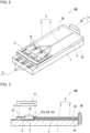
- FIG. 1 is an exploded perspective view of a light-emitting device according to a first embodiment.
- FIG. 2 is a perspective view of the light-emitting device without a lid.
- FIG. 3 is a cross-sectional view of the light-emitting device taken along line III-III in FIG. 2 .
- FIG. 4 is a plan view of the light-emitting device without the lid.
- a light-emitting device 200 according to the first embodiment includes an optical waveguide package 100, light-emitting elements 10 in an element mount 8, and a lid 11 covering the element mount 8.
- the light-emitting device 200 according to the first embodiment further includes a lens 45 on the optical path of light emitted through a core 4.
- the optical waveguide package 100 includes a substrate 1 including a first surface 2, a cladding 3 located on the first surface 2 and including a second surface 3a facing the first surface 2, a third surface 3b opposite to the second surface 3a, and the element mount 8 with an opening in the third surface 3b, and the core 4 located in the cladding 3.
- the optical waveguide package 100 in the first embodiment further includes wires 15 for external connection located on the first surface 2 of the substrate 1.
- the light-emitting device 200 includes three light-emitting elements 10 in the element mount 8 of the optical waveguide package 100.
- Each light-emitting element 10 is, for example, a light-emitting diode (LED) that emits red (R) light, green (G) light, or blue (B) light.
- the core 4 and the cladding 3 may be integral with each other to be an optical waveguide layer 5.
- the substrate 1 may be a ceramic wiring board including dielectric layers made of a ceramic material.
- the ceramic material for the ceramic wiring board include sintered aluminum oxide, sintered mullite, sintered silicon carbide, sintered aluminum nitride, and sintered glass ceramic.
- the substrate 1 may be an organic wiring board including dielectric layers made of, for example, an organic material.
- the organic wiring board may be, for example, a printed wiring board, a build-up wiring board, or a flexible wiring board.
- Examples of the organic material for the organic wiring board include an epoxy resin, a polyimide resin, a polyester resin, an acrylic resin, a phenolic resin, and a fluororesin.
- the core 4 and the cladding 3 are included in the optical waveguide layer 5.
- the optical waveguide layer 5 may be made of, for example, glass such as quartz, or a resin.
- both the core 4 and the cladding 3 may be made of glass or a resin.
- one of the core 4 or the cladding 3 may be made of glass and the other may be made of a resin.
- the core 4 and the cladding 3 have different refractive indexes.
- the core 4 has a higher refractive index than the cladding 3. This difference in refractive index is used to fully reflect light at the interface between the core 4 and the cladding 3. More specifically, a material with a higher refractive index is used to form a path, which is then surrounded by a material with a lower refractive index. This structure confines light in the core 4 with the higher refractive index.
- the core 4 includes multiple incident end faces 4a, 4b, and 4c and one emission end face 42.
- the core 4 includes multiple branching paths 41a, 41b, and 41c, a merging portion 43, and a joined path 44 between the incident end faces 4a, 4b, and 4c and the emission end face 42.
- the branching paths 41a, 41b, and 41c respectively include the incident end faces 4a, 4b, and 4c at one end.
- the branching paths 41a, 41b, and 41c merge together at the merging portion 43.
- the joined path 44 includes the emission end face 42 at one end.
- Red (R) light, green (G) light, and blue (B) light emitted from the light-emitting elements 10 enter the respective branching paths 41a, 41b, and 41c through the respective incident end faces 4a, 4b, and 4c, pass through the merging portion 43 and the joined path 44, and are emitted through the emission end face 42.
- the light-emitting elements 10 are positioned in the element mount 8 with the center of each of the incident end faces 4a, 4b, and 4c of the branching paths 41a, 41b, and 41c aligned with the optical axis of the corresponding light-emitting element 10.
- the element mount 8 may be a recess or a through-hole with an opening in the third surface 3b of the cladding 3.
- the element mount 8 is a through-hole extending from the third surface 3b to the second surface 3a of the cladding 3.
- a bond 17 surrounds the opening of the element mount 8 on the third surface 3b of the cladding 3.
- the bond 17 bonds the lid 11 to the third surface 3b of the cladding 3.
- the element mount 8 is sealed airtightly to protect the light-emitting elements 10.
- the lid 11 may be made of a glass material such as quartz, borosilicate, or sapphire.
- the bond 17 may be made of any material that can airtightly bond the lid 11 to the cladding 3, such as Au-Sn or Sn-Ag-Cu solder, an Ag or Cu metal nanoparticle paste, or a glass paste.
- the lens 45 is located on the optical path of light emitted through the core 4.
- the lens 45 may collimate or condense the light emitted through the core 4.
- the lens 45 is, for example, a plano-convex lens with a flat incident surface and a convex emission surface.
- the light-emitting elements 10 are connected to the wires 15 for external connection.
- the wires 15 for external connection extend, for example, from inside the element mounts 8 to outside the element mounts 8 between the second surface 3a of the cladding 3 and the first surface 2 of the substrate 1.
- the lower electrodes are connected directly to the wires 15 for external connection
- the upper electrodes are connected to the wires 15 for external connection with, for example, bonding wires.
- the two electrodes on the lower surface are connected directly to the wires 15 for external connection.
- the light-emitting elements 10 are electrically connected to an external control circuit with, for example, the wires 15 for external connection.
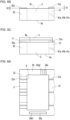
- FIG. 5A is an enlarged plan view of the cladding 3 in the first embodiment.
- FIG. 5B is an enlarged side view of the cladding 3 in the first embodiment.
- FIG. 5C is an enlarged side view of the cladding 3 and the lid 11 in the first embodiment.
- the cladding 3 includes a first portion 31 having the core 4 inside, and a second portion 32 facing the first portion 31 across the element mount 8.
- the first portion 31 includes multiple first protrusions 31a in a first area of the third surface 3b corresponding to the first portion 31.
- the second portion 32 includes multiple second protrusions 32a in a second area of the third surface 3b corresponding to the second portion 32.
- the light-emitting elements 10 are mounted closer to the first portion 31 having the core 4 inside than to the second portion 32 of the cladding 3 in the element mount 8.
- the light-emitting elements 10 generate heat during operation.
- the first portion 31 closer to the light-emitting elements 10 has a higher temperature than the second portion 32.
- the first portion 31 and the second portion 32 have a temperature difference.
- the cladding 3, the lid 11, and the bond 17 made of different materials may have different thermal expansions caused by the temperature difference between the first portion 31 and the second portion 32.
- the lid 11 may thus partially separate from the cladding 3, causing deterioration in airtightness.
- the first portion 31 includes the first protrusions 31a
- the second portion 32 includes the second protrusions 32a.
- the bonding area between the bond 17 and the cladding 3 is larger than when the cladding 3 has a flat surface. This improves the bonding strength and reduces deterioration in airtightness.
- the first protrusions 31a and the second protrusions 32a extend in, for example, a first direction in which the first portion 31 and the second portion 32 face each other with a temperature difference between them.
- the first direction herein is the lateral direction in FIGs. 4 to 5C .
- the first protrusions 31a are located above the core 4.
- the first protrusions 31a are fewer than the second protrusions 32a.
- the first protrusions 31a have a less width and a greater height than the second protrusions 32a.
- a height h1 of the first protrusions 31a and a height h2 of the second protrusions 32a are the dimensions from the third surface 3b of the cladding 3.
- a width w1 of the first protrusions 31a and a width w2 of the second protrusions 32a are the dimensions in a direction (second direction) perpendicular to the first direction in which the first protrusions 31a and the second protrusions 32a extend.
- This structure allows high adhesion to the lid 11 and thus improves reliability, although the portion adjacent to the first protrusions 31a has higher temperatures than the portion adjacent to the second protrusions 32a. This structure also allows the portion adjacent to the second protrusions 32a to have high adhesion to the lid 11 with the less likelihood of tilting of the lid 11 covering the element mount 8.
- the first protrusions 31a and the second protrusions 32a may be formed by, for example, chemically treating, or for example, etching, or physically machining the third surface 3b of the cladding 3. Rods, strips, and others may be placed to form recesses and protrusions on the portions of the first surface 2 of the substrate 1 corresponding to the first portion 31 and the second portion 32 of the cladding 3.
- recesses and protrusions are formed on the first portion 31 and the second portion 32 of the cladding 3 along the recesses and the protrusions on the first surface 2 of the substrate 1.
- the protrusions formed as described above serve as the first protrusions 31a and the second protrusions 32a.
- the first protrusions 31a and the second protrusions 32a may also be formed by placing, for example, the rods and the strips inside the cladding 3.
- the first portion 31 may have the first protrusions 31a along the core 4 inside the cladding 3
- the second portion 32 may have the second protrusions 32a along the wires 15 for external connection on the first surface 2 of the substrate 1.
- FIG. 6A is an enlarged plan view of a cladding in the second embodiment.
- FIGs. 6B and 6C are enlarged side views of the cladding in the second embodiment.
- FIG. 6D is an enlarged side view of the cladding and a lid in the second embodiment.
- the second embodiment is the same as the first embodiment except the structure of the cladding 3.
- the cladding 3 further includes a third portion 33 between the first portion 31 and the second portion 32.
- the third portion 33 includes third protrusions 33a in a third area of the third surface 3b corresponding to the third portion 33.
- the third protrusions 33a further increase the bonding area between the bond 17 and the cladding 3 to improve the bonding strength and reduce deterioration in airtightness.
- the third protrusions 33a include at least one of a protrusion 33a1 extending in the first direction in which the first portion 31 and the second portion 32 face each other or a protrusion 33a2 extending in the second direction perpendicular to the first direction.
- the third protrusions 33a include the protrusion 33a1 extending in the first direction and the protrusion 33a2 extending in the second direction.
- the third protrusions 33a may include the protrusion 33a1 alone or the protrusion 33a2 alone. With the third protrusions 33a including the protrusion 33a1 and the protrusion 33a2, the bond 17 is deformable in the two directions when thermally expanded, with further reduction of the stress caused by the thermal expansion.
- the third protrusions 33a include the protrusion 33a1 extending in the first direction in which the first portion 31 and the second portion 32 face each other and the protrusion 33a2 extending in the second direction perpendicular to the first direction in the above example, the protrusion 33a2 may extend in a direction intersecting with the first direction and produces the same or similar advantageous effects as described above.
- FIG. 7A is an enlarged plan view of a cladding in the third embodiment.
- FIG. 7B is an enlarged side view of the cladding in the third embodiment.
- FIG. 7C is an enlarged side view of the cladding and a lid in the third embodiment.
- the third embodiment is the same as the first embodiment except the structure of the cladding 3.
- the cladding 3 has a distance d1 between the second surface 3 a and the first area of the third surface 3b that is shorter than a distance d2 between the second surface 3a and the second area of the third surface 3b.
- the first portion 31 has a thickness tl less than a thickness t2 of the second portion 32.
- the third portion 33 between the first portion 31 and the second portion 32 may have the same thickness as, for example, the first portion 31 or the second portion 32.
- the third portion 33 has the same thickness as the second portion 32 in a portion adjacent to the second portion 32, and has the same thickness as the first portion 31 in a portion adjacent to the first portion 31.
- the third portion 33 thus includes a step.
- the third portion 33 may have a thickness continuously decreasing from the portion adjacent to the second portion 32 toward the portion adjacent to first portion 31. In this case, the third area of the third surface 3b is tilted.
- FIG. 8 is a plan view of a light-emitting device according to a fourth embodiment without a lid 11.
- the core 4 includes the three branching paths 41a, 41b, and 41c merged at the merging portion 43 to be the single joined path 44 including the single emission end face 42.
- the light-emitting device including an optical waveguide package according to the fourth embodiment may include three independent cores 44a, 44b, and 44c as in the plan view in FIG. 8 .
- the incident end faces 4a, 4b, and 4c of the three cores 44a, 44b, and 44c each have the center aligned with the optical axis of the corresponding light-emitting element 10.
- the three incident end faces 4a, 4b, and 4c are thus located apart from one another to align with the respective light-emitting elements 10.
- the three cores 44a, 44b, and 44c in the present embodiment include emission end faces 42a, 42b, and 42c located adjacent to one another.
- the three cores 44a, 44b, and 44c may be gathered adjacent to one another between the incident end faces 4a, 4b, and 4c and the emission end faces 42a, 42b, and 42c, and extend parallel to one another to the emission end faces 42a, 42b, and 42c.
- Light beams from the emission end faces 42a, 42b, and 42c of the respective cores may be emitted parallel to one another through, for example, the single lens 45.
- the images or others resulting from the emission light beams from the three emission end faces 42a, 42b, and 42c may be combined using, for example, an external device.
- the lid 11 is bonded parallel to the third surface 3b of the cladding 3.
- the bond 17 levels the third surface 3b of the cladding 3 with any steps, recesses, or protrusions to maintain the lid 11 in parallel without being tilted.
- the cladding 3 has the first portion 31 thinner than the second portion 32.
- the bond 17 is thus thicker on the first portion 31 than on the second portion 32, maintaining the lid 11 in parallel without being tilted.
- the amount of the bond 17 on the first portion 31 that can have a higher temperature is greater than on the second portion 32 that can have a lower temperature. This reduces the difference in thermal expansion between the portions of the bond 17 resulting from the temperature difference. This reduces the likelihood of separation of the lid 11, thus reducing deterioration in airtightness.
- the bond 17 is, for example, Au-Sn solder
- the bond 17 thicker on the first portion 31 can improve light-shielding and reduce light leakage between the lid 11 and the cladding 3.
- the light-emitting elements 10 are not limited to LEDs, and may be, for example, laser diodes (LDs) or vertical-cavity surface-emitting lasers (VCSELs).
- LDs laser diodes
- VCSELs vertical-cavity surface-emitting lasers
- the light-emitting device may be implemented in forms (1) to (6) below.
- the light-emitting device has less deterioration in airtightness.
Landscapes
- Physics & Mathematics (AREA)
- General Physics & Mathematics (AREA)
- Optics & Photonics (AREA)
- Condensed Matter Physics & Semiconductors (AREA)
- Electromagnetism (AREA)
- Engineering & Computer Science (AREA)
- Microelectronics & Electronic Packaging (AREA)
- Optical Couplings Of Light Guides (AREA)
- Led Device Packages (AREA)
Abstract
Description
- The present disclosure relates to a light-emitting device.
- A known light-emitting device is described in, for example,
Patent Literature 1. - Patent Literature 1:
Japanese Unexamined Patent Application Publication No. 10-308555 - In an aspect of the present disclosure, a light-emitting device includes a substrate including a first surface, a cladding on the first surface and including a second surface facing the first surface, a third surface opposite to the second surface, and an element mount with an opening in the third surface, a core in the cladding, a light-emitting element in the element mount, and a lid covering the element mount. The cladding includes a first portion having the core inside, and a second portion facing the first portion across the element mount. The first portion includes a plurality of first protrusions in a first area of the third surface corresponding to the first portion. The second portion includes a plurality of second protrusions in a second area of the third surface corresponding to the second portion.
- The objects, features, and advantages of the present disclosure will become more apparent from the following detailed description and the drawings.
-
FIG. 1 is an exploded perspective view of a light-emitting device according to a first embodiment. -
FIG. 2 is a perspective view of the light-emitting device without a lid. -
FIG. 3 is a cross-sectional view of the light-emitting device taken along line III-III inFIG. 2 . -
FIG. 4 is a plan view of the light-emitting device without the lid. -
FIG. 5A is an enlarged plan view of a cladding in the first embodiment. -
FIG. 5B is an enlarged side view of the cladding in the first embodiment. -
FIG. 5C is an enlarged side view of the cladding and the lid in the first embodiment. -
FIG. 6A is an enlarged plan view of a cladding in a second embodiment. -
FIG. 6B is an enlarged side view of the cladding in the second embodiment. -
FIG. 6C is an enlarged side view of the cladding in the second embodiment. -
FIG. 6D is an enlarged side view of the cladding and a lid in the second embodiment. -
FIG. 7A is an enlarged plan view of a cladding in a third embodiment. -
FIG. 7B is an enlarged side view of the cladding in the third embodiment. -
FIG. 7C is an enlarged side view of the cladding and a lid in the third embodiment. -
FIG. 8 is a plan view of a light-emitting device according to a fourth embodiment without a lid. - A light-emitting device with the structure that forms the basis of a light-emitting device according to one or more embodiments of the present disclosure will be described first.
-
Patent Literature 1 describes a hybrid waveguide optical circuit having a recessed cutout in a cladding on a substrate to receive an optical element. The cutout is covered airtightly with a sealing lid. The hybrid waveguide optical circuit includes a surface planarizing layer surrounding the optical-element mount at least on the surface of the cladding or inside the cladding. This minimizes the amount of fixing agent used to fix the sealing lid to the cladding surface. - The light-emitting element generates heat, which transfers through the cladding. The light-emitting element is mounted near a core. The portion of the cladding having the core inside thus has a temperature different from the temperature of the other portion. This temperature difference causes different thermal expansions among the lid, the cladding, and a bond. The lid may thus partially separate from the cladding, possibly causing deterioration in airtightness.
- The light-emitting device according to one or more embodiments of the present disclosure will now be described with reference to the accompanying drawings.
FIG. 1 is an exploded perspective view of a light-emitting device according to a first embodiment.FIG. 2 is a perspective view of the light-emitting device without a lid.FIG. 3 is a cross-sectional view of the light-emitting device taken along line III-III inFIG. 2 .FIG. 4 is a plan view of the light-emitting device without the lid. - A light-
emitting device 200 according to the first embodiment includes anoptical waveguide package 100, light-emitting elements 10 in anelement mount 8, and alid 11 covering theelement mount 8. The light-emitting device 200 according to the first embodiment further includes alens 45 on the optical path of light emitted through acore 4. Theoptical waveguide package 100 includes asubstrate 1 including afirst surface 2, acladding 3 located on thefirst surface 2 and including asecond surface 3a facing thefirst surface 2, athird surface 3b opposite to thesecond surface 3a, and theelement mount 8 with an opening in thethird surface 3b, and thecore 4 located in thecladding 3. Theoptical waveguide package 100 in the first embodiment further includeswires 15 for external connection located on thefirst surface 2 of thesubstrate 1. - In the present embodiment, the light-
emitting device 200 includes three light-emitting elements 10 in theelement mount 8 of theoptical waveguide package 100. Each light-emittingelement 10 is, for example, a light-emitting diode (LED) that emits red (R) light, green (G) light, or blue (B) light. Thecore 4 and thecladding 3 may be integral with each other to be anoptical waveguide layer 5. - The
substrate 1 may be a ceramic wiring board including dielectric layers made of a ceramic material. Examples of the ceramic material for the ceramic wiring board include sintered aluminum oxide, sintered mullite, sintered silicon carbide, sintered aluminum nitride, and sintered glass ceramic. - The
substrate 1 may be an organic wiring board including dielectric layers made of, for example, an organic material. The organic wiring board may be, for example, a printed wiring board, a build-up wiring board, or a flexible wiring board. Examples of the organic material for the organic wiring board include an epoxy resin, a polyimide resin, a polyester resin, an acrylic resin, a phenolic resin, and a fluororesin. - The
core 4 and thecladding 3 are included in theoptical waveguide layer 5. Theoptical waveguide layer 5 may be made of, for example, glass such as quartz, or a resin. In theoptical waveguide layer 5, both thecore 4 and thecladding 3 may be made of glass or a resin. In some embodiments, one of thecore 4 or thecladding 3 may be made of glass and the other may be made of a resin. Thecore 4 and thecladding 3 have different refractive indexes. Thecore 4 has a higher refractive index than thecladding 3. This difference in refractive index is used to fully reflect light at the interface between thecore 4 and thecladding 3. More specifically, a material with a higher refractive index is used to form a path, which is then surrounded by a material with a lower refractive index. This structure confines light in thecore 4 with the higher refractive index. - The
core 4 includes multiple incident end faces 4a, 4b, and 4c and oneemission end face 42. Thecore 4 includes multiple branchingpaths portion 43, and a joinedpath 44 between the incident end faces 4a, 4b, and 4c and theemission end face 42. The branchingpaths paths portion 43. The joinedpath 44 includes the emission end face 42 at one end. - Red (R) light, green (G) light, and blue (B) light emitted from the light-emitting
elements 10 enter the respective branchingpaths portion 43 and the joinedpath 44, and are emitted through theemission end face 42. The light-emittingelements 10 are positioned in theelement mount 8 with the center of each of the incident end faces 4a, 4b, and 4c of the branchingpaths element 10. - The
element mount 8 may be a recess or a through-hole with an opening in thethird surface 3b of thecladding 3. In the present embodiment, theelement mount 8 is a through-hole extending from thethird surface 3b to thesecond surface 3a of thecladding 3. In a plan view, abond 17 surrounds the opening of theelement mount 8 on thethird surface 3b of thecladding 3. Thebond 17 bonds thelid 11 to thethird surface 3b of thecladding 3. Theelement mount 8 is sealed airtightly to protect the light-emittingelements 10. - The
lid 11 may be made of a glass material such as quartz, borosilicate, or sapphire. Thebond 17 may be made of any material that can airtightly bond thelid 11 to thecladding 3, such as Au-Sn or Sn-Ag-Cu solder, an Ag or Cu metal nanoparticle paste, or a glass paste. - The
lens 45 is located on the optical path of light emitted through thecore 4. Thelens 45 may collimate or condense the light emitted through thecore 4. Thelens 45 is, for example, a plano-convex lens with a flat incident surface and a convex emission surface. - In the present embodiment, the light-emitting
elements 10 are connected to thewires 15 for external connection. Thewires 15 for external connection extend, for example, from inside the element mounts 8 to outside the element mounts 8 between thesecond surface 3a of thecladding 3 and thefirst surface 2 of thesubstrate 1. For light-emittingelements 10 with electrodes on their lower and upper surfaces, the lower electrodes are connected directly to thewires 15 for external connection, and the upper electrodes are connected to thewires 15 for external connection with, for example, bonding wires. For light-emittingelements 10 with electrodes on their lower surfaces, the two electrodes on the lower surface are connected directly to thewires 15 for external connection. The light-emittingelements 10 are electrically connected to an external control circuit with, for example, thewires 15 for external connection. - The
element mount 8 of thecladding 3 and its adjacent area will be described.FIG. 5A is an enlarged plan view of thecladding 3 in the first embodiment.FIG. 5B is an enlarged side view of thecladding 3 in the first embodiment.FIG. 5C is an enlarged side view of thecladding 3 and thelid 11 in the first embodiment. Thecladding 3 includes afirst portion 31 having thecore 4 inside, and asecond portion 32 facing thefirst portion 31 across theelement mount 8. Thefirst portion 31 includes multiplefirst protrusions 31a in a first area of thethird surface 3b corresponding to thefirst portion 31. Thesecond portion 32 includes multiplesecond protrusions 32a in a second area of thethird surface 3b corresponding to thesecond portion 32. - To allow light emitted from the light-emitting
elements 10 to enter the respective incident end faces 4a, 4b, and 4c, the light-emittingelements 10 are mounted closer to thefirst portion 31 having thecore 4 inside than to thesecond portion 32 of thecladding 3 in theelement mount 8. The light-emittingelements 10 generate heat during operation. In thecladding 3, thefirst portion 31 closer to the light-emittingelements 10 has a higher temperature than thesecond portion 32. In other words, thefirst portion 31 and thesecond portion 32 have a temperature difference. Thecladding 3, thelid 11, and thebond 17 made of different materials may have different thermal expansions caused by the temperature difference between thefirst portion 31 and thesecond portion 32. Thelid 11 may thus partially separate from thecladding 3, causing deterioration in airtightness. In the present embodiment, thefirst portion 31 includes thefirst protrusions 31a, and thesecond portion 32 includes thesecond protrusions 32a. The bonding area between thebond 17 and thecladding 3 is larger than when thecladding 3 has a flat surface. This improves the bonding strength and reduces deterioration in airtightness. - The
first protrusions 31a and thesecond protrusions 32a extend in, for example, a first direction in which thefirst portion 31 and thesecond portion 32 face each other with a temperature difference between them. When thermally expanded, thebond 17 is deformable along thefirst protrusions 31a and thesecond protrusions 32a, reducing the stress caused by the thermal expansion. The first direction herein is the lateral direction inFIGs. 4 to 5C . - In the present embodiment, the
first protrusions 31a are located above thecore 4. Thefirst protrusions 31a are fewer than thesecond protrusions 32a. Thefirst protrusions 31a have a less width and a greater height than thesecond protrusions 32a. A height h1 of thefirst protrusions 31a and a height h2 of thesecond protrusions 32a are the dimensions from thethird surface 3b of thecladding 3. A width w1 of thefirst protrusions 31a and a width w2 of thesecond protrusions 32a are the dimensions in a direction (second direction) perpendicular to the first direction in which thefirst protrusions 31a and thesecond protrusions 32a extend. This structure allows high adhesion to thelid 11 and thus improves reliability, although the portion adjacent to thefirst protrusions 31a has higher temperatures than the portion adjacent to thesecond protrusions 32a. This structure also allows the portion adjacent to thesecond protrusions 32a to have high adhesion to thelid 11 with the less likelihood of tilting of thelid 11 covering theelement mount 8. - The
first protrusions 31a and thesecond protrusions 32a may be formed by, for example, chemically treating, or for example, etching, or physically machining thethird surface 3b of thecladding 3. Rods, strips, and others may be placed to form recesses and protrusions on the portions of thefirst surface 2 of thesubstrate 1 corresponding to thefirst portion 31 and thesecond portion 32 of thecladding 3. When thecladding 3 is formed on thefirst surface 2, recesses and protrusions are formed on thefirst portion 31 and thesecond portion 32 of thecladding 3 along the recesses and the protrusions on thefirst surface 2 of thesubstrate 1. The protrusions formed as described above serve as thefirst protrusions 31a and thesecond protrusions 32a. Thefirst protrusions 31a and thesecond protrusions 32a may also be formed by placing, for example, the rods and the strips inside thecladding 3. For example, thefirst portion 31 may have thefirst protrusions 31a along thecore 4 inside thecladding 3, and thesecond portion 32 may have thesecond protrusions 32a along thewires 15 for external connection on thefirst surface 2 of thesubstrate 1. - A light-emitting device according to a second embodiment will be described.
FIG. 6A is an enlarged plan view of a cladding in the second embodiment.FIGs. 6B and 6C are enlarged side views of the cladding in the second embodiment.FIG. 6D is an enlarged side view of the cladding and a lid in the second embodiment. The second embodiment is the same as the first embodiment except the structure of thecladding 3. The other components will not be described in detail. In the present embodiment, thecladding 3 further includes athird portion 33 between thefirst portion 31 and thesecond portion 32. Thethird portion 33 includesthird protrusions 33a in a third area of thethird surface 3b corresponding to thethird portion 33. In the present embodiment, thethird protrusions 33a further increase the bonding area between thebond 17 and thecladding 3 to improve the bonding strength and reduce deterioration in airtightness. - The
third protrusions 33a include at least one of a protrusion 33a1 extending in the first direction in which thefirst portion 31 and thesecond portion 32 face each other or a protrusion 33a2 extending in the second direction perpendicular to the first direction. In the present embodiment, thethird protrusions 33a include the protrusion 33a1 extending in the first direction and the protrusion 33a2 extending in the second direction. Thethird protrusions 33a may include the protrusion 33a1 alone or the protrusion 33a2 alone. With thethird protrusions 33a including the protrusion 33a1 and the protrusion 33a2, thebond 17 is deformable in the two directions when thermally expanded, with further reduction of the stress caused by the thermal expansion. Although thethird protrusions 33a include the protrusion 33a1 extending in the first direction in which thefirst portion 31 and thesecond portion 32 face each other and the protrusion 33a2 extending in the second direction perpendicular to the first direction in the above example, the protrusion 33a2 may extend in a direction intersecting with the first direction and produces the same or similar advantageous effects as described above. - A light-emitting device according to a third embodiment will be described.
FIG. 7A is an enlarged plan view of a cladding in the third embodiment.FIG. 7B is an enlarged side view of the cladding in the third embodiment.FIG. 7C is an enlarged side view of the cladding and a lid in the third embodiment. The third embodiment is the same as the first embodiment except the structure of thecladding 3. The other components will not be described in detail. In the present embodiment, thecladding 3 has a distance d1 between thesecond surface 3 a and the first area of thethird surface 3b that is shorter than a distance d2 between thesecond surface 3a and the second area of thethird surface 3b. In other words, thefirst portion 31 has a thickness tl less than a thickness t2 of thesecond portion 32. - The
third portion 33 between thefirst portion 31 and thesecond portion 32 may have the same thickness as, for example, thefirst portion 31 or thesecond portion 32. In the present embodiment, thethird portion 33 has the same thickness as thesecond portion 32 in a portion adjacent to thesecond portion 32, and has the same thickness as thefirst portion 31 in a portion adjacent to thefirst portion 31. Thethird portion 33 thus includes a step. Thethird portion 33 may have a thickness continuously decreasing from the portion adjacent to thesecond portion 32 toward the portion adjacent tofirst portion 31. In this case, the third area of thethird surface 3b is tilted. -
FIG. 8 is a plan view of a light-emitting device according to a fourth embodiment without alid 11. In the first to third embodiments, thecore 4 includes the three branchingpaths portion 43 to be the single joinedpath 44 including the singleemission end face 42. The light-emitting device including an optical waveguide package according to the fourth embodiment may include threeindependent cores FIG. 8 . As in the above embodiments, the incident end faces 4a, 4b, and 4c of the threecores element 10. The three incident end faces 4a, 4b, and 4c are thus located apart from one another to align with the respective light-emittingelements 10. The threecores cores single lens 45. The images or others resulting from the emission light beams from the three emission end faces 42a, 42b, and 42c may be combined using, for example, an external device. - The
lid 11 is bonded parallel to thethird surface 3b of thecladding 3. Thebond 17 levels thethird surface 3b of thecladding 3 with any steps, recesses, or protrusions to maintain thelid 11 in parallel without being tilted. In the present embodiment, thecladding 3 has thefirst portion 31 thinner than thesecond portion 32. Thebond 17 is thus thicker on thefirst portion 31 than on thesecond portion 32, maintaining thelid 11 in parallel without being tilted. The amount of thebond 17 on thefirst portion 31 that can have a higher temperature is greater than on thesecond portion 32 that can have a lower temperature. This reduces the difference in thermal expansion between the portions of thebond 17 resulting from the temperature difference. This reduces the likelihood of separation of thelid 11, thus reducing deterioration in airtightness. - When the
bond 17 is, for example, Au-Sn solder, thebond 17 thicker on thefirst portion 31 can improve light-shielding and reduce light leakage between thelid 11 and thecladding 3. - The light-emitting
elements 10 are not limited to LEDs, and may be, for example, laser diodes (LDs) or vertical-cavity surface-emitting lasers (VCSELs). - The light-emitting device according to one or more embodiments of the present disclosure may be implemented in forms (1) to (6) below.
- (1) A light-emitting device, comprising:
- a substrate including a first surface;
- a cladding on the first surface, the cladding including a second surface facing the first surface, a third surface opposite to the second surface, and an element mount with an opening in the third surface;
- a core in the cladding;
- a light-emitting element in the element mount; and
- a lid covering the element mount,
- wherein the cladding includes a first portion having the core inside, and a second portion facing the first portion across the element mount,
- the first portion includes a plurality of first protrusions in a first area of the third surface corresponding to the first portion, and
- the second portion includes a plurality of second protrusions in a second area of the third surface corresponding to the second portion.
- (2) The light-emitting device according to (1), wherein
- the plurality of first protrusions is located above the core,
- the plurality of first protrusions is fewer than the plurality of second protrusions,
- the plurality of first protrusions has a less width than the plurality of second protrusions, and
- the plurality of first protrusions has a greater height than the plurality of second protrusions.
- (3) The light-emitting device according to (1) or (2), wherein
- the cladding further includes a third portion between the first portion and the second portion, and
- the third portion includes a third protrusion in a third area of the third surface corresponding to the third portion.
- (4) The light-emitting device according to (3), wherein
the third protrusion includes at least one of a protrusion extending in a first direction in which the first portion and the second portion face each other or a protrusion extending in a second direction perpendicular to the first direction. - (5) The light-emitting device according to any one of (1) to (4), wherein
a distance between the second surface and the first area of the third surface is shorter than a distance between the second surface and the second area of the third surface. - (6) The light-emitting device according to any one of (1) to (5), further comprising:
a lens on an optical path of light to be emitted through the core. - The light-emitting device according to one or more embodiments of the present disclosure has less deterioration in airtightness.
- Although the embodiments of the present disclosure have been described in detail, the present disclosure is not limited to the embodiments described above, and may be changed or varied in various manners without departing from the spirit and scope of the present disclosure. The components described in the above embodiments may be entirely or partially combined as appropriate unless any contradiction arises.
-
- 1 substrate
- 2 first surface
- 3 cladding
- 3a second surface
- 3b third surface
- 4; 44a, 44b, 44c core
- 4a, 4b, 4c incident end face
- 5 optical waveguide layer
- 8 element mount
- 10 light-emitting element
- 11 lid
- 15 wire for external connection
- 17 bond
- 31 first portion
- 31a first protrusion
- 32 second portion
- 32a second protrusion
- 33 third portion
- 33a third protrusion
- 33a1 protrusion
- 33a2 protrusion
- 41a branching path
- 42; 42a, 42b, 42cemission end face
- 43 merging portion
- 44 joined path
- 45 lens
- 100 optical waveguide package
- 200 light-emitting device
Claims (6)
- A light-emitting device, comprising:a substrate including a first surface;a cladding on the first surface, the cladding including a second surface facing the first surface, a third surface opposite to the second surface, and an element mount with an opening in the third surface;a core in the cladding;a light-emitting element in the element mount; anda lid covering the element mount,wherein the cladding includes a first portion having the core inside, and a second portion facing the first portion across the element mount,the first portion includes a plurality of first protrusions in a first area of the third surface corresponding to the first portion, andthe second portion includes a plurality of second protrusions in a second area of the third surface corresponding to the second portion.
- The light-emitting device according to claim 1, whereinthe plurality of first protrusions is located above the core,the plurality of first protrusions is fewer than the plurality of second protrusions,the plurality of first protrusions has a less width than the plurality of second protrusions, andthe plurality of first protrusions has a greater height than the plurality of second protrusions.
- The light-emitting device according to claim 1 or claim 2, whereinthe cladding further includes a third portion between the first portion and the second portion, andthe third portion includes a third protrusion in a third area of the third surface corresponding to the third portion.
- The light-emitting device according to claim 3, wherein
the third protrusion includes at least one of a protrusion extending in a first direction in which the first portion and the second portion face each other or a protrusion extending in a second direction perpendicular to the first direction. - The light-emitting device according to any one of claims 1 to 4, wherein
a distance between the second surface and the first area of the third surface is shorter than a distance between the second surface and the second area of the third surface. - The light-emitting device according to any one of claims 1 to 5, further comprising:
a lens on an optical path of light to be emitted through the core.
Applications Claiming Priority (2)
| Application Number | Priority Date | Filing Date | Title |
|---|---|---|---|
| JP2021146101 | 2021-09-08 | ||
| PCT/JP2022/033314 WO2023038014A1 (en) | 2021-09-08 | 2022-09-05 | Light-emitting device |
Publications (2)
| Publication Number | Publication Date |
|---|---|
| EP4400879A1 true EP4400879A1 (en) | 2024-07-17 |
| EP4400879A4 EP4400879A4 (en) | 2025-08-27 |
Family
ID=85507636
Family Applications (1)
| Application Number | Title | Priority Date | Filing Date |
|---|---|---|---|
| EP22867336.4A Pending EP4400879A4 (en) | 2021-09-08 | 2022-09-05 | LIGHT-EMITTING DEVICE |
Country Status (6)
| Country | Link |
|---|---|
| US (1) | US12222540B2 (en) |
| EP (1) | EP4400879A4 (en) |
| JP (1) | JP7703672B2 (en) |
| CN (1) | CN117980790A (en) |
| TW (1) | TWI836593B (en) |
| WO (1) | WO2023038014A1 (en) |
Families Citing this family (1)
| Publication number | Priority date | Publication date | Assignee | Title |
|---|---|---|---|---|
| CN118998669A (en) * | 2024-10-09 | 2024-11-22 | 邵树发 | LED light string with optical fiber |
Family Cites Families (15)
| Publication number | Priority date | Publication date | Assignee | Title |
|---|---|---|---|---|
| JPH05341143A (en) * | 1992-06-04 | 1993-12-24 | Hitachi Cable Ltd | Surface mount bidirectional transmission module |
| JP3674061B2 (en) | 1994-10-31 | 2005-07-20 | 株式会社日立製作所 | Thin film multilayer circuit board and optical waveguide manufacturing method |
| JP3758258B2 (en) * | 1996-11-29 | 2006-03-22 | 富士通株式会社 | Optical coupling device |
| US6112002A (en) * | 1996-11-29 | 2000-08-29 | Fujitsu Limited | Optical coupler optically coupling a light beam of a semiconductor laser source with a single mode optical waveguide or fiber |
| JPH10308555A (en) * | 1997-05-01 | 1998-11-17 | Nippon Telegr & Teleph Corp <Ntt> | Hybrid waveguide type optical circuit and manufacturing method thereof |
| JP4203837B2 (en) | 1999-10-13 | 2009-01-07 | 富士通株式会社 | Optical transmission module |
| KR20030094466A (en) * | 2002-06-04 | 2003-12-12 | 주식회사일진 | Optical Module with Multiport |
| JP4553026B2 (en) * | 2008-03-27 | 2010-09-29 | 富士ゼロックス株式会社 | Optical transmission equipment |
| EP2613188B1 (en) * | 2010-08-31 | 2019-01-23 | Kyocera Corporation | Optical transmission substrate and optical transmission module |
| US20130064512A1 (en) * | 2011-09-08 | 2013-03-14 | Nayana Ghantiwala | Cooling system for an optical module |
| EP3385692A1 (en) * | 2017-04-03 | 2018-10-10 | Indigo Diabetes N.V. | Hermeticity testing of an optical assembly |
| JP7081356B2 (en) * | 2018-07-17 | 2022-06-07 | 日本電信電話株式会社 | Optical fiber guide parts and optical connection structure |
| JP7280031B2 (en) * | 2018-11-14 | 2023-05-23 | 新光電気工業株式会社 | Optical waveguide mounting substrate, optical communication device, and method for manufacturing optical waveguide mounting substrate |
| EP4040517A4 (en) * | 2019-09-30 | 2023-10-25 | Kyocera Corporation | HOUSING FOR OPTICAL WAVE GUIDES AND LIGHT EMITTING DEVICE |
| TWM617324U (en) * | 2019-10-31 | 2021-09-21 | 佑勝光電股份有限公司 | Optical transceiver module and an optical cable module |
-
2022
- 2022-09-05 WO PCT/JP2022/033314 patent/WO2023038014A1/en not_active Ceased
- 2022-09-05 JP JP2023546939A patent/JP7703672B2/en active Active
- 2022-09-05 EP EP22867336.4A patent/EP4400879A4/en active Pending
- 2022-09-05 US US18/689,746 patent/US12222540B2/en active Active
- 2022-09-05 CN CN202280060624.5A patent/CN117980790A/en active Pending
- 2022-09-07 TW TW111133888A patent/TWI836593B/en active
Also Published As
| Publication number | Publication date |
|---|---|
| TWI836593B (en) | 2024-03-21 |
| JPWO2023038014A1 (en) | 2023-03-16 |
| EP4400879A4 (en) | 2025-08-27 |
| US20240377575A1 (en) | 2024-11-14 |
| JP7703672B2 (en) | 2025-07-07 |
| US12222540B2 (en) | 2025-02-11 |
| CN117980790A (en) | 2024-05-03 |
| TW202320364A (en) | 2023-05-16 |
| WO2023038014A1 (en) | 2023-03-16 |
Similar Documents
| Publication | Publication Date | Title |
|---|---|---|
| US12181723B2 (en) | Optical waveguide package and light-emitting device | |
| JP7783528B2 (en) | Light-emitting device and base | |
| EP4040516A1 (en) | Optical waveguide package and light emitting device | |
| US20230358978A1 (en) | Optical waveguide package, light emitter, and projection system | |
| EP4400879A1 (en) | Light-emitting device | |
| EP4160705B1 (en) | Optical waveguide package and light emitting device | |
| US20220373736A1 (en) | Optical waveguide package and light-emitting device | |
| EP4478098A1 (en) | Optical waveguide substrate, optical waveguide package, and light source module | |
| JPWO2020162023A1 (en) | Semiconductor light emitting device | |
| EP4398321A1 (en) | Optical waveguide package and light-emitting device | |
| US20250306319A1 (en) | Optical waveguide package and light-emitting device | |
| US12276823B2 (en) | Light source module | |
| EP4297205A1 (en) | Light emitting device | |
| EP4350401A1 (en) | Light source module |
Legal Events
| Date | Code | Title | Description |
|---|---|---|---|
| STAA | Information on the status of an ep patent application or granted ep patent |
Free format text: STATUS: THE INTERNATIONAL PUBLICATION HAS BEEN MADE |
|
| PUAI | Public reference made under article 153(3) epc to a published international application that has entered the european phase |
Free format text: ORIGINAL CODE: 0009012 |
|
| STAA | Information on the status of an ep patent application or granted ep patent |
Free format text: STATUS: REQUEST FOR EXAMINATION WAS MADE |
|
| 17P | Request for examination filed |
Effective date: 20240307 |
|
| AK | Designated contracting states |
Kind code of ref document: A1 Designated state(s): AL AT BE BG CH CY CZ DE DK EE ES FI FR GB GR HR HU IE IS IT LI LT LU LV MC MK MT NL NO PL PT RO RS SE SI SK SM TR |
|
| DAV | Request for validation of the european patent (deleted) | ||
| DAX | Request for extension of the european patent (deleted) | ||
| A4 | Supplementary search report drawn up and despatched |
Effective date: 20250725 |
|
| RIC1 | Information provided on ipc code assigned before grant |
Ipc: G02B 6/12 20060101AFI20250721BHEP Ipc: G02B 6/42 20060101ALI20250721BHEP Ipc: H01S 5/0225 20210101ALI20250721BHEP |