EP4400847A1 - Detection apparatus, shunt circuit and terminal device - Google Patents
Detection apparatus, shunt circuit and terminal device Download PDFInfo
- Publication number
- EP4400847A1 EP4400847A1 EP21960216.6A EP21960216A EP4400847A1 EP 4400847 A1 EP4400847 A1 EP 4400847A1 EP 21960216 A EP21960216 A EP 21960216A EP 4400847 A1 EP4400847 A1 EP 4400847A1
- Authority
- EP
- European Patent Office
- Prior art keywords
- shunt
- signal
- circuit
- signals
- current
- Prior art date
- Legal status (The legal status is an assumption and is not a legal conclusion. Google has not performed a legal analysis and makes no representation as to the accuracy of the status listed.)
- Pending
Links
- 238000001514 detection method Methods 0.000 title claims abstract description 129
- 230000003287 optical effect Effects 0.000 claims abstract description 52
- 238000006243 chemical reaction Methods 0.000 claims abstract description 39
- 238000012545 processing Methods 0.000 claims description 128
- 230000003321 amplification Effects 0.000 claims description 89
- 238000003199 nucleic acid amplification method Methods 0.000 claims description 89
- 238000000034 method Methods 0.000 claims description 23
- 239000003990 capacitor Substances 0.000 claims description 14
- 229920006395 saturated elastomer Polymers 0.000 abstract description 14
- 238000013461 design Methods 0.000 description 42
- 238000010586 diagram Methods 0.000 description 23
- 238000004590 computer program Methods 0.000 description 7
- 230000009286 beneficial effect Effects 0.000 description 6
- 230000003750 conditioning effect Effects 0.000 description 6
- 230000006870 function Effects 0.000 description 6
- 238000013507 mapping Methods 0.000 description 5
- 238000005516 engineering process Methods 0.000 description 4
- 230000003190 augmentative effect Effects 0.000 description 2
- 230000008878 coupling Effects 0.000 description 2
- 238000010168 coupling process Methods 0.000 description 2
- 238000005859 coupling reaction Methods 0.000 description 2
- 230000005669 field effect Effects 0.000 description 2
- 230000007774 longterm Effects 0.000 description 2
- 238000004519 manufacturing process Methods 0.000 description 2
- 239000004065 semiconductor Substances 0.000 description 2
- 238000011161 development Methods 0.000 description 1
- 230000000694 effects Effects 0.000 description 1
- 229910044991 metal oxide Inorganic materials 0.000 description 1
- 150000004706 metal oxides Chemical class 0.000 description 1
- 238000012986 modification Methods 0.000 description 1
- 230000004048 modification Effects 0.000 description 1
Images




Classifications
-
- G—PHYSICS
- G01—MEASURING; TESTING
- G01S—RADIO DIRECTION-FINDING; RADIO NAVIGATION; DETERMINING DISTANCE OR VELOCITY BY USE OF RADIO WAVES; LOCATING OR PRESENCE-DETECTING BY USE OF THE REFLECTION OR RERADIATION OF RADIO WAVES; ANALOGOUS ARRANGEMENTS USING OTHER WAVES
- G01S17/00—Systems using the reflection or reradiation of electromagnetic waves other than radio waves, e.g. lidar systems
- G01S17/02—Systems using the reflection of electromagnetic waves other than radio waves
- G01S17/06—Systems determining position data of a target
- G01S17/08—Systems determining position data of a target for measuring distance only
- G01S17/10—Systems determining position data of a target for measuring distance only using transmission of interrupted, pulse-modulated waves
-
- G—PHYSICS
- G01—MEASURING; TESTING
- G01S—RADIO DIRECTION-FINDING; RADIO NAVIGATION; DETERMINING DISTANCE OR VELOCITY BY USE OF RADIO WAVES; LOCATING OR PRESENCE-DETECTING BY USE OF THE REFLECTION OR RERADIATION OF RADIO WAVES; ANALOGOUS ARRANGEMENTS USING OTHER WAVES
- G01S7/00—Details of systems according to groups G01S13/00, G01S15/00, G01S17/00
- G01S7/48—Details of systems according to groups G01S13/00, G01S15/00, G01S17/00 of systems according to group G01S17/00
- G01S7/4808—Evaluating distance, position or velocity data
-
- G—PHYSICS
- G01—MEASURING; TESTING
- G01S—RADIO DIRECTION-FINDING; RADIO NAVIGATION; DETERMINING DISTANCE OR VELOCITY BY USE OF RADIO WAVES; LOCATING OR PRESENCE-DETECTING BY USE OF THE REFLECTION OR RERADIATION OF RADIO WAVES; ANALOGOUS ARRANGEMENTS USING OTHER WAVES
- G01S7/00—Details of systems according to groups G01S13/00, G01S15/00, G01S17/00
- G01S7/48—Details of systems according to groups G01S13/00, G01S15/00, G01S17/00 of systems according to group G01S17/00
- G01S7/483—Details of pulse systems
- G01S7/486—Receivers
- G01S7/4861—Circuits for detection, sampling, integration or read-out
-
- G—PHYSICS
- G01—MEASURING; TESTING
- G01S—RADIO DIRECTION-FINDING; RADIO NAVIGATION; DETERMINING DISTANCE OR VELOCITY BY USE OF RADIO WAVES; LOCATING OR PRESENCE-DETECTING BY USE OF THE REFLECTION OR RERADIATION OF RADIO WAVES; ANALOGOUS ARRANGEMENTS USING OTHER WAVES
- G01S7/00—Details of systems according to groups G01S13/00, G01S15/00, G01S17/00
- G01S7/48—Details of systems according to groups G01S13/00, G01S15/00, G01S17/00 of systems according to group G01S17/00
- G01S7/483—Details of pulse systems
- G01S7/486—Receivers
- G01S7/4868—Controlling received signal intensity or exposure of sensor
-
- G—PHYSICS
- G01—MEASURING; TESTING
- G01S—RADIO DIRECTION-FINDING; RADIO NAVIGATION; DETERMINING DISTANCE OR VELOCITY BY USE OF RADIO WAVES; LOCATING OR PRESENCE-DETECTING BY USE OF THE REFLECTION OR RERADIATION OF RADIO WAVES; ANALOGOUS ARRANGEMENTS USING OTHER WAVES
- G01S17/00—Systems using the reflection or reradiation of electromagnetic waves other than radio waves, e.g. lidar systems
- G01S17/88—Lidar systems specially adapted for specific applications
- G01S17/93—Lidar systems specially adapted for specific applications for anti-collision purposes
- G01S17/931—Lidar systems specially adapted for specific applications for anti-collision purposes of land vehicles
Definitions
- This application relates to the field of lidar technologies, and in particular, to a detection apparatus, a shunt circuit, and a terminal device.
- a laser detection apparatus mainly includes a laser transmitter, a laser receiver, and a processor.
- the laser transmitter may transmit a laser signal.
- the laser signal is reflected after encountering an object.
- the laser receiver can detect the reflected signal, convert the reflected signal into an electrical signal, and perform corresponding processing (for example, amplification or conversion) on the electrical signal and output the electrical signal to the processor.
- the processor can determine a distance between the laser detection apparatus and the object and luminous intensity information of the reflected signal.
- a luminous intensity of the reflected signal is high (for example, the luminous intensity exceeds 5,000 cd)
- the electrical signal obtained by the laser receiver through conversion of the reflected signal exceeds a range of signals that can be received by the processor, and the processor cannot accurately obtain the electrical signal corresponding to the reflected signal. Consequently, the processor cannot accurately determine the distance between the laser detection apparatus and the object and the luminous intensity information of the reflected signal. Therefore, a luminous intensity range of reflected signals that can be detected by the laser detection apparatus is limited.
- Embodiments of this application provide a detection apparatus, a shunt circuit, and a terminal device, to improve a luminous intensity range of reflected signals that can be detected by the detection apparatus.
- the method may be applied to the Internet of vehicles, for example, vehicle-to-everything (vehicle-to-everything, V2X), a long term evolution-vehicle (long term evolution-vehicle, LTE-V) technology, and vehicle to vehicle (vehicle-vehicle, V2V).
- V2X vehicle-to-everything
- LTE-V long term evolution-vehicle
- V2V vehicle to vehicle
- an embodiment of this application provides a detection apparatus.
- the detection apparatus may include a detection unit, an optical-to-electrical conversion unit, and a shunt circuit.
- the detection unit may be configured to receive an optical signal including a reflected signal of a laser transmit signal.
- the optical-to-electrical conversion unit may be configured to perform optical-to-electrical conversion on the received optical signal, to obtain a current signal including a first current signal.
- the shunt circuit may be configured to shunt the first current signal to obtain N second current signals used to generate N second voltage signals V i .
- N is an integer greater than or equal to 1
- i is an integer greater than or equal to 1 and less than or equal to N.
- the shunt circuit may shunt the first current signal in the current signal, to obtain the N second current signals.
- the N second current signals may be used to generate a plurality of voltage signals, so that the detection apparatus may output a plurality of voltage signals.
- the "high luminous intensity” may be understood as that the luminous intensity of the current reflected signal exceeds the luminous intensity range of the reflected signals that can be detected by the detection apparatus.
- Different detection apparatuses may correspond to different luminous intensity ranges. For example, for a laser detection apparatus, a luminous intensity range is from 500 cd to 5,000 cd. For another example, for an infrared light detection apparatus, a luminous intensity range is from 100 cd to 1,000 cd.
- a current value of the current signal obtained by performing optical-to-electrical conversion on the optical signal by the optical-to-electrical conversion unit is greater than a preset threshold.
- the shunt circuit shunts the first current signal in the current signal only when the current value of the current signal corresponding to the reflected signal of a target object is greater than the preset threshold, to obtain a plurality of second current signals, and the plurality of second current signals may be used to generate a plurality of second voltage signals.
- the N second voltage signals V i may be used to determine distance information of a target object generating the reflected signal and/or intensity information of the optical signal.
- the N second voltage signals are not saturated, the distance information of the target object and/or the intensity information of the optical signal that are/is determined based on the N second voltage signals are/is more accurate.
- the shunt circuit may shunt the first current signal based on N preset first control signals, to obtain the N second current signals.
- One preset first control signal may correspond to one bias voltage
- the N preset first control signals correspond to N bias voltages VB i .
- Values of the N bias voltages may be the same or different. This is not specifically limited in this embodiment of this application.
- the N preset first control signals are in a one-to-one correspondence with the N second current signals.
- one second current signal may be obtained by shunting the first current signal based on one preset first control signal.
- the shunt circuit may shunt the first current signal based on the N preset first control signals, so that the shunt circuit can quickly shunt the first current signal, and a next-stage processing circuit can receive a voltage signal corresponding to the reflected signal more quickly, thereby effectively improving efficiency of determining information about a distance between the target object and the detection apparatus and/or the intensity information of the optical signal.
- the shunt circuit may include N second shunt circuits, and the N second shunt circuits may shunt the first current signal based on the N preset first control signals, to obtain the N second current signals.
- each of the N second shunt circuits is in a one-to-one correspondence with each of the N preset first control signals, and each first control signal is in a one-to-one correspondence with each of the N second current signals.
- each second shunt circuit may shunt the first current signal based on a first control signal corresponding to the second shunt circuit, to obtain one second current signal.
- a second shunt circuit 1 shunts the first current signal based on a first control signal 1, to obtain a second current signal 1.
- a second shunt circuit 2 shunts the first current signal based on a first control signal 2, to obtain a second current signal 2.
- the N second shunt circuits that are in a one-to-one correspondence with the N preset first control signals are disposed in the shunt circuit, so that each second shunt circuit may shunt the first current signal based on the first control signal corresponding to the second shunt circuit, and each second shunt circuit may obtain a second current signal that meets a preset dynamic range (namely, a value range of the current signal) of the second shunt circuit.
- the shunt circuit may further shunt the first current signal based on received N second control signals, to obtain N fourth current signals used to generate N third voltage signals V i' .
- One second control signal may correspond to one bias voltage, and the N second control signals correspond to N bias voltages VB i' . Values of the N bias voltages may be the same or different. This is not specifically limited in this embodiment of this application.
- the "received N second control signals" may be received by the shunt circuit from a next-stage processing circuit.
- the next-stage processing circuit may be an external processing circuit of the detection apparatus or an internal processing circuit of the detection apparatus.
- the N second control signals may be dynamically determined based on the N second voltage signals output by the shunt circuit. For example, a second control signal 1 is determined based on a second voltage signal V 1 , and a second control signal 2 is determined based on a second voltage signal 2.
- the N third voltage signals V i' may be used to determine the distance information of the target object generating the reflected signal and/or the intensity information of the optical signal.
- the N third voltage signals are not saturated, the information about the distance between the target object and the detection apparatus and/or the intensity information of the optical signal that are/is determined based on the N third voltage signals V i' are more accurate.
- the shunt circuit further includes a first shunt circuit, and the current signal further includes a third current signal.
- the first shunt circuit may be configured to shunt the third current signal used to generate a first voltage signal V 0 .
- the first shunt circuit shunts some current signals that are less than the preset threshold and that are in the current signal corresponding to the reflected signal, to obtain the third current signal, so that the some current signals can be quickly output.
- a current value corresponding to the third current signal is less than the preset threshold.
- the first voltage signal V 0 may be used to determine the distance information of the target object generating the reflected signal and/or the intensity information of the optical signal.
- the first voltage signal generated based on the third current signal may be used to determine the distance information of the target object generating the reflected signal and/or the intensity information of the optical signal, so that the distance information of the target object and/or the intensity information of the optical signal that are/is determined by the detection apparatus are/is more accurate.
- an embodiment of this application further provides a shunt circuit.
- the shunt circuit may be a shunt circuit in the foregoing detection apparatus.
- the shunt circuit may include a first node N 1 , N second shunt circuits, and N processing circuits.
- the first node N 1 is coupled to input ends of the N second shunt circuits, and output ends of the N second shunt circuits are respectively coupled to input ends of the N processing circuits.
- N is an integer greater than or equal to 1.
- the first node N 1 may be configured to input a first current signal to the N second shunt circuits.
- the N second shunt circuits may be configured to shunt the first current signal to obtain N second current signals.
- the N processing circuits may be configured to process the N second current signals to generate N second voltage signals V i .
- the N second shunt circuits and the N processing circuits are disposed in the shunt circuit, so that each second shunt circuit may shunt the first current signal to obtain corresponding second current signals, and the processing circuits corresponding to the second shunt circuits may further process the second current signals to generate the second voltage signals.
- the shunt circuit may output a plurality of voltage signals, so that the voltage signals output by the shunt circuit are not saturated.
- the N second voltage signals may be used to determine distance information of a target object generating a reflected signal and/or intensity information of an optical signal.
- the shunt circuit may further include a first component and a first shunt circuit.
- An output end of the first component is coupled to an input end of the first shunt circuit, and the output end of the first component is coupled to input ends of the N second shunt circuits through the first node N 1 .
- the first component may be configured to obtain a current signal including the first current signal and a third current signal.
- the first shunt circuit may be configured to shunt the current signal to obtain the third current signal used to generate a first voltage signal V 0 .
- the first component configured to obtain the current signal is disposed, and the output end of the first component is coupled to both the input end of the first shunt circuit and the input ends of the N second shunt circuits, so that the current signal is shunted.
- the N second current signals and the third current signal that are obtained after shunting may generate a plurality of voltage signals, so that the voltage signals output by the shunt circuit are not saturated.
- the first voltage signal V 0 may be used to determine the distance information of the target object generating the reflected signal and/or the intensity information of the optical signal.
- a current value of the current signal is greater than a preset threshold, and a current value of the third current signal is less than the preset threshold.
- the N second shunt circuits may shunt the first current signal based on the N preset first control signals, to obtain the N second current signals.
- the N processing circuits may be further configured to receive the N second control signals.
- the N second shunt circuits may be further configured to shunt the first current signal based on the N second control signals, to obtain N fourth current signals.
- the N processing circuits may be further configured to process the N fourth current signals, to obtain N third voltage signals V i' .
- an i th second shunt circuit in the N second shunt circuits may include a discharge circuit D i .
- Each of the N processing circuits includes a first resistor R sensor , a second node N 2 , a first capacitor C 1 , and an amplification circuit.
- An input end of the discharge circuit D i is coupled to the first node N 1 .
- the first resistor R sensor is coupled to both an output end of the discharge circuit D i and an input end of the amplification circuit.
- One end of the first capacitor C 1 is coupled to both the first resistor R sensor and the input end of the amplification circuit through the second node N 2 , and the other end is grounded.
- the discharge circuit D i may be configured to shunt the first current signal, to obtain the second current signals.
- the first resistor R sensor may be configured to convert the second current signals into fourth voltage signals, and input the fourth voltage signals to the amplification circuit.
- the amplification circuit may be configured to amplify the fourth voltage signals to obtain the second voltage signals V i .
- the processing circuits may convert the second current signals obtained by the discharge circuit through shunting into voltage signals, and further amplify and output the voltage signals. In this way, a next-stage processing circuit can capture an accurate voltage signal, so that the distance information of the target object and/or the intensity information of the optical signal that are/is determined are/is more accurate.
- the discharge circuit D i may be one of the following components: a diode, a metal-oxide-semiconductor (metal oxide semiconductor field effect transistor, MOS) field-effect transistor, or a transistor.
- MOS metal oxide semiconductor field effect transistor
- the discharge circuit has many implementations, so that implementation of the discharge circuit is simplified and complexity of the circuit is reduced.
- the amplification circuit in the processing circuits has a plurality of implementations, including but not limited to the following:
- the amplification circuit includes a first amplification circuit, and the first amplification circuit may be configured to amplify the fourth voltage signals, to obtain the second voltage signals V i .
- the first amplification circuit may include a second amplifier T 2 , and the second amplifier T 2 may include one or more amplifiers. This is not specifically limited in this embodiment of this application.
- the amplification circuit may include a logarithmic amplification circuit and a second amplification circuit. An input end of the logarithmic amplification circuit is coupled to the first resistor R sensor , and an output end of the logarithmic amplification circuit may be coupled to an input end of the second amplification circuit.
- the logarithmic amplification circuit may be configured to amplify the fourth voltage signals to obtain fifth voltage signals.
- the second amplification circuit may be configured to amplify the fifth voltage signals to obtain the second voltage signals V i .
- the logarithmic amplification circuit and the second amplification circuit are designed in the amplification circuit, so that a dynamic range (namely, a range of an output voltage) of the amplification circuit is effectively increased, and the second voltage signals output by the processing circuits can be more easily captured by a next-stage processing circuit.
- the logarithmic amplification circuit may include a second amplifier T 2 , a second resistor R 1 , an equivalent diode D 3 , a third node N 3 , and a second capacitor C 2 .
- the second amplification circuit includes a third amplifier T 3 .
- One end of the second resistor R 1 is coupled to an output end of the second amplifier T 2 , and the other end is coupled to both an input end of the equivalent diode D 3 and an input end of the third amplifier T 3 .
- One end of the second capacitor C 2 is coupled to an output end of the equivalent diode D 3 through the third node N 3 , and the other end is grounded.
- the second amplifier T 2 after performing logarithmic amplification on the voltage signals obtained by converting the second current signals, the second amplifier T 2 outputs the voltage signals to the third amplifier T 3 , so that the third amplifier T 3 may further amplify the voltage signals obtained after the logarithmic amplification, to obtain the second voltage signals corresponding to the second current signals.
- the equivalent diode D 3 may be any one of the diode, the MOS transistor, or the transistor. In this design, the equivalent diode D 3 has a plurality of implementations, and complexity of the logarithmic amplification circuit is effectively reduced.
- the first component is an optical-to-electrical converter, and the first component may be further configured to receive an optical signal and convert the optical signal into a current signal.
- the first component has a function of optical-to-electrical signal conversion, so that the shunt circuit can shunt the current signal corresponding to the optical signal reflected by the target object.
- the first shunt circuit may include a first amplifier T 1 .
- the first amplifier T 1 may be configured to: convert the third current signal obtained by the first shunt circuit through shunting to obtain a corresponding voltage signal, and amplify the voltage signal to obtain the first voltage signal.
- the first amplifier T 1 is disposed in the first shunt circuit, so that implementation of the first shunt circuit is simple.
- the first amplifier T 1 may be one or more amplifiers. This is not specifically limited in this embodiment of this application.
- an embodiment of this application provides a terminal device, including the detection apparatus according to any one of the first aspect and the possible designs of the first aspect.
- some terminal devices include but are not limited to: a smart home device (such as a television, a robotic vacuum cleaner, a smart desk lamp, a speaker system, a smart lighting system, an electrical control system, home background music, a home theater system, an intercom system, or video surveillance), an intelligent transportation device (such as a vehicle, a ship, an uncrewed aerial vehicle, a train, a wagon, or a truck), an intelligent manufacturing device (such as a robot, an industrial device, intelligent logistics, or a smart factory), and an intelligent terminal (such as a mobile phone, a computer, a tablet computer, a palmtop computer, a desktop computer, a headset, a speaker, a wearable device, a vehicle-mounted device, a virtual reality device, or an augmented reality device).
- a smart home device such as a television, a robotic vacuum cleaner, a smart desk lamp,
- a and/or B may represent the following cases: Only A exists, both A and B exist, and only B exists, where A and B may be singular or plural.
- Terms such as “first”, “second” and “third” are merely used for distinction and description, and shall not be understood as an indication or implication of relative importance or an indication or implication of an order.
- a "first control signal” and a “second control signal” mentioned below are merely used to indicate different control signals, and do not have different sequences, priorities, or importance degrees.
- a detection apparatus may be used to detect a distance of a target object.
- a laser detection apparatus 100 is used as an example of the detection apparatus.
- the laser detection apparatus 100 may include a laser transmitter 1, a laser receiver 2, and a processing circuit 3.
- the laser transmitter 1 may transmit a laser signal. After receiving the laser signal, a target object 4 reflects a corresponding optical signal (namely, a reflected signal).
- the laser receiver 2 may detect the reflected signal reflected by the target object 4, convert the reflected signal to obtain a corresponding voltage signal, and input the voltage signal to the processing circuit 3.
- the processing circuit 3 may determine a distance between the target object 4 and the laser detection apparatus 100 and intensity information of the reflected signal based on the voltage signal.
- FIG. 2 is a possible schematic diagram of a structure of the laser receiver 2.
- Vcc is an optical signal input end of the laser receiver 2
- V bias is a control signal input end of the laser receiver 2
- V out is an output end of the laser receiver 2.
- the laser receiver 2 includes an optical-to-electrical converter 201 and an amplification circuit 202.
- the optical-to-electrical converter 201 may convert an optical signal received from the input end Vcc of the laser receiver 2, to obtain a current signal, and input the current signal to the amplification circuit 202.
- the amplification circuit 202 includes an amplifier T 0 and a resistor R 0 .
- the amplifier T 0 may convert, based on a control signal input by the control signal input end V bias , the current signal to obtain a voltage signal 1, amplify the voltage signal 1 to obtain a voltage signal 2, and output the voltage signal 2 through the output end V out .
- the amplification circuit 202 may output the voltage signal 2 to the processing circuit 3.
- the processing circuit 3 may perform analog-to-digital conversion on the voltage signal 2, to obtain a time at which the reflected signal is returned from the target object 4 to the laser receiver 2, and then calculate a distance between the target object 4 and the laser detection apparatus 100 and intensity information of the reflected signal of the target object 4 based on the time.
- the voltages output by the laser receiver 2 avoid being saturated, so that the laser detection apparatus 100 can accurately detect the distance of the target object and/or the intensity information of the reflected signal of the target object, to increase a detection range of the laser detection apparatus.
- the detection apparatus includes a detection unit, an optical-to-electrical conversion unit, and a shunt circuit.
- the detection unit may be configured to receive an optical signal including a reflected signal of a laser transmit signal.
- the optical-to-electrical conversion unit may be configured to perform optical-to-electrical conversion on the received optical signal, to obtain a current signal including a first current signal.
- the shunt circuit may be configured to shunt the first current signal to obtain N second current signals used to generate N second voltage signals V i .
- N is an integer greater than or equal to 1
- i is an integer greater than or equal to 1 and less than or equal to N.
- the shunt circuit is disposed in the detection apparatus.
- the shunt circuit may shunt the first current signal, to obtain the N second current signals.
- Each second current signal may generate one voltage signal, so that the detection apparatus may output a plurality of voltage signals.
- voltage signals obtained after the detection apparatus processes the current signal corresponding to the reflected signal are not saturated (namely, within a value range of voltage signals that can be received by a next-stage processing circuit), thereby effectively increasing a luminous intensity range of reflected signals that can be detected by the detection apparatus.
- the "reflected signal with a high luminous intensity” may be understood as that the luminous intensity of the current reflected signal exceeds the luminous intensity range of the reflected signals that can be detected by the detection apparatus.
- a laser includes infrared light, ultraviolet light, and the like.
- different laser detection apparatuses can detect reflected signals of different luminous intensity ranges.
- a luminous intensity range of reflected signals that can be detected by an infrared light detection apparatus is from 500 cd to 5,000 cd.
- a luminous intensity range of reflected signals that can be detected by an ultraviolet light detection apparatus is from 100 cd to 1,000 cd.
- the detection apparatus may be a laser detection apparatus.
- the laser detection apparatus may be mounted on the vehicle. In this way, in a traveling process of the vehicle, the laser detection apparatus may detect a laser signal reflected by a target object.
- the laser detection apparatus can determine a current signal corresponding to the laser signal, shunt the current signal to obtain a plurality of current signals, and process the plurality of current signals to obtain a plurality of voltage signals. In this way, the laser detection apparatus can output a plurality of voltage signals, so that the voltage signals output by the laser detection apparatus are not saturated.
- the laser detection apparatus when detecting a reflected signal with a high luminous intensity, can also accurately obtain information about a distance between the target object and the laser detection apparatus and/or intensity information of the laser signal reflected by the target object, thereby effectively increasing a luminous intensity range of reflected signals that can be detected by the laser detection apparatus, and further determining more obstacles on a pavement by the laser detection apparatus. In this way, the vehicle can optimize a traveling trajectory of the vehicle, thereby effectively improving safety of autonomous driving or assisted driving.
- the laser detection apparatus may further have another application scenario.
- the infrared light detection apparatus may be mounted on the uncrewed aerial vehicle.
- the infrared light detection apparatus may detect an infrared light signal reflected by a target object.
- the infrared light detection apparatus shunts a current signal generated by the infrared light signal, to obtain a plurality of current signals, thereby generating a plurality of voltage signals and effectively avoiding voltage signals output by the infrared light detection apparatus from being saturated.
- the infrared light detection apparatus can accurately determine a distance between the target object and the infrared light detection apparatus based on the infrared light signal, so that when the uncrewed aerial vehicle enters a danger range (that is, the target object in the danger range is detected), an alarm may be generated for the uncrewed aerial vehicle.
- the laser detection apparatus may also be an ultraviolet light detection apparatus, a visible light detection apparatus, or the like. Examples are not described herein again.
- the detection apparatus disclosed in this embodiment of this application may be applied to a terminal device having a signal processing capability.
- the detection apparatus may be a terminal device or an independent unit.
- the unit may be embedded in a terminal device.
- the terminal device may shunt a current signal corresponding to the reflected signal, so that voltage signals output by the detection apparatus are not saturated (namely, within a value range of voltage signals that can be received by a next-stage processing circuit), thereby effectively increasing a luminous intensity range of reflected signals that can be detected by the detection apparatus.
- the terminal device may be an intelligent device having a signal processing capability, including but not limited to: a smart home device, such as a television, a robotic vacuum cleaner, a smart desk lamp, a speaker system, an intelligent lighting system, an electrical control system, home background music, a home theater system, an intercom system, or video surveillance; an intelligent transportation device, such as a vehicle, a ship, an uncrewed aerial vehicle, a train, a wagon, or a truck; and an intelligent manufacturing device, such as a robot or an industrial device.
- the terminal device may be a computer device having a signal processing capability, such as a desktop computer, a personal computer, or a server.
- the terminal device may alternatively be a portable electronic device having a shunting capability, such as a mobile phone, a tablet computer, a palmtop computer, a headset, a speaker, a wearable device (such as a smart watch), a vehicle-mounted device, a virtual reality device, or an augmented reality device.
- a portable electronic device having a shunting capability such as a mobile phone, a tablet computer, a palmtop computer, a headset, a speaker, a wearable device (such as a smart watch), a vehicle-mounted device, a virtual reality device, or an augmented reality device.
- Coupled in the following embodiment of this application may be an electrical connection, and an electrical connection between two electrical elements may be a direct or indirect connection between the two electrical elements.
- a connection between A and B may be either a direct connection between A and B, or an indirect connection between A and B through one or more other electrical elements.
- the connection between A and B may be that A and C are directly connected, C and B are directly connected, and A and B are connected through C.
- coupling between A and B enables electric energy to be transmitted between A and B.
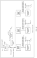
- FIG. 3 is a schematic diagram of a circuit structure of a detection apparatus according to an embodiment of this application.
- the detection apparatus may include a detection unit 301, an optical-to-electrical conversion unit 302, and a shunt circuit 303.
- An input end a 1 of the detection unit 301 is configured to receive an optical signal.
- An output end a 2 of the detection unit 301 is coupled to an input end b 1 of the optical-to-electrical conversion unit 302, and is configured to input the received optical signal to the optical-to-electrical conversion unit 302.
- An output end b 2 of the optical-to-electrical conversion unit 302 is coupled to an input end c 1 of the shunt circuit 303.
- the optical signal includes a reflected signal of a laser transmit signal.
- the optical-to-electrical conversion unit 302 may be configured to perform optical-to-electrical conversion on the received optical signal to obtain a current signal 1, and input the current signal 1 to the shunt circuit 303.
- the current signal 1 includes a first current signal.
- the shunt circuit 303 may be configured to shunt the first current signal to obtain N second current signals used to generate N second voltage signals.
- N is an integer greater than or equal to 1.
- the shunt circuit 303 may shunt the first current signal, one or more second voltage signals are generated, so that voltage signals corresponding to optical signals with a high luminous intensity detected by the detection apparatus are not saturated (namely, within a value range of voltage signals that can be received by a next-stage processing circuit), and a luminous intensity range of reflected signals that can be detected by the detection apparatus is effectively increased.
- the shunt circuit 303 shunts the first current signal in a plurality of implementations, including but not limited to the following:
- the shunt circuit 303 may shunt the first current signal based on N preset first control signals to obtain N second current signals used to generate N second voltage signals V i .
- each preset first control signal corresponds to a preset bias voltage
- the preset bias voltage is a bias voltage preconfigured in the shunt circuit 303 when technical personnel design the shunt circuit 303.
- a quantity of N is not specifically limited in this embodiment of this application.
- N is 4, and the shunt circuit 303 may shunt the first current signal based on four preset first control signals to obtain four second current signals, and then may obtain four second voltage signals V 1 , V 2 , V 3 , and V 4 based on the four current signals.
- the N preset first control signals are in a one-to-one correspondence with the N second current signals.
- one second current signal may be obtained by shunting the first current signal based on a bias voltage corresponding to one first control signal.
- the shunt circuit 303 may shunt the first current signal based on the bias voltage VB 1 , to obtain a second current signal 1.
- the shunt circuit 303 may shunt the first current signal based on the bias voltage VB 2 , to obtain a second current signal 2.
- a first control signal 3 corresponds to a bias voltage VB 3
- the shunt circuit 303 may shunt the first current signal based on the bias voltage VB 3 , to obtain a second current signal 3.
- the shunt circuit 303 directly shunts the first current signal based on the preset first control signals, thereby effectively improving shunting efficiency of the shunt circuit 303.
- the shunt circuit 303 may shunt the first current signal based on N preset first control signals to obtain N second current signals used to generate N second voltage signals V i . Then, the shunt circuit 303 further shunts the first current signal based on received N second control signals to obtain N fourth current signals used to generate N third voltage signals V i' .
- the "received N second control signals" may be received by the shunt circuit 303 from a next-stage processing circuit.
- the next-stage processing circuit may be an external processing circuit of the detection apparatus 300 or an internal processing circuit of the detection apparatus 300.
- One received second control signal may correspond to one bias voltage VB i'
- received N second control signals correspond to N bias voltages.
- Current values corresponding to the N second current signals are different from current values corresponding to the fourth current signals, and voltage values corresponding to the N second voltage signals are different from voltage values corresponding to the N third voltage signals.
- one fourth current signal may be obtained by shunting the first current signal based on a bias voltage corresponding to one second control signal.
- the shunt circuit 303 may shunt the first current signal based on the bias voltage VB 1' , to obtain a fourth current signal 1.
- the shunt circuit 303 may shunt the first current signal based on the bias voltage VB 2' , to obtain a fourth current signal 2.
- the shunt circuit 303 may shunt the first current signal based on the bias voltage VB 3' , to obtain a fourth current signal 3.
- first control signal refers to related descriptions in Manner 1.
- the N second control signals are determined after the N first control signals are determined.
- the shunt circuit 303 may convert the N second current signals into the N second voltage signals, and output the N second voltage signals to a next-stage processing circuit.
- the next-stage processing circuit may determine the N bias voltages corresponding to the N second control signals based on the N second voltage signals. A larger voltage value corresponding to the second voltage signal indicates a larger bias voltage value that is corresponding to the second control signal and that is set by the next-stage processing circuit.
- the next-stage processing circuit may determine the bias voltage value corresponding to the second control signal based on the mapping relationship.
- a bias voltage corresponding to a second control signal 1 is 75 V; if a voltage value corresponding to a second voltage signal 2 is 50 V, a bias voltage corresponding to a second control signal 2 is 55 V; and if a voltage value corresponding to a second voltage signal 3 is 30 V, a bias voltage corresponding to a second control signal 3 is 35 V
- mapping relationship in Table 1 is merely an example, and is not limited. More mapping relationships may exist between the voltage value corresponding to the second voltage signal and the bias voltage value corresponding to the second control signal, provided that the voltage value corresponding to the second voltage signal is directly proportional to the bias voltage value corresponding to the second control signal.
- FIG. 4A is a schematic diagram of a possible structure of a shunt circuit 303.
- N is 4, and the shunt circuit 303 in FIG. 4A includes a first subcircuit and a second subcircuit.
- the first subcircuit in the shunt circuit 303 may receive a current signal 1, shunt a first current signal in the current signal 1 based on four preset first control signals to obtain four second current signals, and input the four second current signals to the second subcircuit in the shunt circuit 303.
- the second subcircuit in the shunt circuit 303 obtains four second voltage signals, V 1 , V 2 , V 3 , and V 4 , based on the four second current signals, and inputs the four second voltage signals to a next-stage processing circuit.
- the next-stage processing circuit determines four second control signals based on the four second voltage signals and mapping relationships between voltage values corresponding to the second voltage signals and bias voltage values corresponding to the second control signals, and inputs the four second control signals to the first subcircuit in the shunt circuit 303. As shown in (b) in FIG.
- the first subcircuit in the shunt circuit 303 may shunt the first current signal again based on the four second control signals to obtain four fourth current signals, and input the four fourth current signals to the second subcircuit in the shunt circuit 303.
- the second sub circuit in the shunt circuit 303 obtains four third voltage signals, V 1' , V 2' , V 3' , and V 4' based on the four second current signals, and inputs the four third voltage signals to the next-stage processing circuit.
- the shunt circuit 303 may further shunt the first current signal again based on the N second control signals, to obtain the N fourth current signals.
- the N second control signals are dynamically determined based on the N second voltage signals, so that the third voltage signals determined based on the fourth current signals obtained through shunting can better adapt to a voltage receiving range of a next-stage processing circuit.
- the N second voltage signals or the N third voltage signals may be used to determine distance information of a target object generating a reflected signal and/or intensity information of an optical signal.
- FIG. 4B is a schematic diagram of a possible structure of a shunt circuit 303.
- the shunt circuit 303 may include: a first node N 1 , N second shunt circuits (namely, second shunt circuits 1 to N), and N processing circuits (namely, a processing circuit 1, a processing circuit 2, ..., and a processing circuit N).
- the first node N 1 is coupled to each input end of the N second shunt circuits, and output ends of the N second shunt circuits are respectively coupled to input ends of the N processing circuits.
- N is an integer greater than or equal to 1.
- the first node N 1 is an electrical node formed by connecting the N second shunt circuits, and is a connection point of the N second shunt circuits in actual hardware.
- the first node N 1 may be configured to input a first current signal to the N second shunt circuits, and then each of the N second shunt circuits may shunt the first current signal to obtain N second current signals.
- Each second shunt circuit may input the second current signal obtained through shunting to a processing circuit corresponding to the second shunt circuit, and then the processing circuit may process the second current signal to generate a second voltage signal.
- the N processing circuits may process the N second current signals to obtain N second voltage signals.
- N second shunt circuits may be in a one-to-one correspondence with the N processing circuits.
- a second shunt circuit 1 corresponds to a processing circuit 1
- a second shunt circuit 2 corresponds to a processing circuit 2
- a second shunt circuit N corresponds to a processing circuit N.
- the second shunt circuit 1 may shunt the first current signal to obtain a second current signal I 1 , and input the second current signal I 1 to the corresponding processing circuit 1, and then the processing circuit 1 may process the second current signal I 1 to generate a second voltage signal V 1 .
- the second shunt circuit 2 may shunt the first current signal to obtain a second current signal I 2 , and input the second current signal I 2 to the corresponding processing circuit 2, and then the processing circuit 2 may process the second current signal I 2 to generate a second voltage signal V 2 .
- the second shunt circuit N may shunt the first current signal to obtain a second current signal I n , and input the second current signal I n to the corresponding processing circuit N, and then the processing circuit N may process the second current signal I n to generate a second voltage signal V N .
- the processing circuit 1 to the processing circuit N further include control signal input ends VB 1 to VB N .
- the processing circuit 1 to the processing circuit N may input corresponding control signals into the N second shunt circuits, and then the N second shunt circuits may shunt the first current based on the control signals.
- the N second shunt circuits shunt the first current signal in a plurality of implementations, including but not limited to the following: Manner 1: The N second shunt circuits may shunt the first current signal based on N preset first control signals to obtain N second current signals used to generate N second voltage signals.
- the N second shunt circuits are in a one-to-one correspondence with the N preset first control signals, and the N preset first control signals are in a one-to-one correspondence with the N second current signals.
- one second shunt circuit may shunt the first current signal based on a bias voltage corresponding to one first control signal, to obtain one second current signal.
- a second shunt circuit 1 may shunt the first current signal based on a bias voltage VB 1 corresponding to a first control signal 1, to obtain a second current signal 1.
- a second shunt circuit 2 may shunt the first current signal based on a bias voltage VB 2 corresponding to a first control signal 2, to obtain a second current signal 2.
- a second shunt circuit 3 may shunt the first current signal based on a bias voltage VB 3 corresponding to a first control signal 3, to obtain a second current signal 3.
- One preset first control signal may correspond to one preset bias voltage, and the N preset first control signals correspond to N preset bias voltages. Values of the N preset bias voltages may be the same or different. This is not specifically limited in this embodiment of this application.
- values of a bias voltage 1 to a bias voltage N may all be 5 V
- values of a bias voltage 1 to a bias voltage 3 are 5 V
- a value of an N th bias voltage among the N bias voltages may be twice a value of an (N+1) th bias voltage.
- N is 1, 2, or 3.
- a value of the bias voltage VB 1 corresponding to the first control signal 1 is 20 V
- a value of the bias voltage VB 2 corresponding to the first control signal 2 is 10 V
- a value of the bias voltage VB 3 corresponding to the first control signal 3 is 5 V
- the N second shunt circuits directly shunt the first current signal based on the preset first control signals, thereby effectively improving shunting efficiency of the N second shunt circuits.
- the N second shunt circuits may shunt the first current signal based on N preset first control signals to obtain N second current signals used to generate N second voltage signals. Then, the N second shunt circuit further shunt the first current signal based on received N second control signals to obtain N fourth current signals used to generate N third voltage signals V i' .
- the N second shunt circuits are in a one-to-one correspondence with the received N second control signals, and the received N first control signals are in a one-to-one correspondence with the N fourth current signals.
- one second shunt circuit may shunt the first current signal based on a bias voltage corresponding to one second control signal, to obtain one fourth current signal.
- a second shunt circuit 1 may shunt the first current signal based on a bias voltage VB 1 corresponding to a second control signal 1, to obtain a fourth current signal 1.
- a second shunt circuit 2 may shunt the first current signal based on a bias voltage VB 2 corresponding to a second control signal 2, to obtain a fourth current signal 2.
- a second shunt circuit 3 may shunt the first current signal based on a bias voltage VB 3 corresponding to a second control signal 3, to obtain a fourth current signal 3.
- a next-stage processing circuit may determine the N bias voltages corresponding to the N second control signals based on the N second voltage signals output by the shunt circuit 303.
- the next-stage processing circuit may determine the N bias voltages corresponding to the N second control signals based on the N second voltage signals output by the N second shunt circuits.
- a larger voltage value corresponding to the second voltage signal indicates a larger bias voltage value that is corresponding to the second control signal and that is set by the next-stage processing circuit.
- N is 3, and a shunt circuit 303 includes a second shunt circuit 1, a second shunt circuit 2, a second shunt circuit 3, a processing circuit 1, a processing circuit 2, and a processing circuit 3.
- the first node N 1 inputs a first current signal to each of the second shunt circuit 1, the second shunt circuit 2, and the second shunt circuit 3.
- the second shunt circuit 1 shunts the first current signal based on a bias voltage VB 1 corresponding to a preset first control signal 1 to obtain a second current signal 1, and inputs the second current signal 1 to the processing circuit 1, and then the processing circuit 1 generates a second voltage signal V 1 based on the second current signal 1, and inputs the second voltage signal V 1 to a next-stage processing circuit.
- the second shunt circuit 2 shunts the first current signal based on a bias voltage VB 2 corresponding to a preset first control signal 2 to obtain a second current signal 2, and inputs the second current signal 2 to the processing circuit 2, and then the processing circuit 2 generates a second voltage signal V 2 based on the second current signal 2, and inputs the second voltage signal V 2 to a next-stage processing circuit.
- the second shunt circuit 3 shunts the first current signal based on a bias voltage VB 3 corresponding to a preset first control signal 3 to obtain a second current signal 3, and inputs the second current signal 3 to the processing circuit 3, and then the processing circuit 3 generates a second voltage signal V 3 based on the second current signal 3, and inputs the second voltage signal V 3 to a next-stage processing circuit.
- the next-stage processing circuit determines a second control signal 1, a second control signal 2, and a second control signal 3 according to the second voltage signal V 1 , the second voltage signal V 2 , and the second voltage signal V 3 .
- the next-stage processing circuit inputs the second control signal 1 to the processing circuit 1.
- the processing circuit 1 converts the second control signal 1 into a corresponding voltage signal VB 1' , and inputs the voltage signal VB 1' to the second shunt circuit 1.
- the second shunt circuit 1 shunts the first current signal again based on the voltage signal VB 1' to obtain a fourth current signal 1, and inputs the fourth current signal 1 to the processing circuit 1.
- the processing circuit 1 generates a third voltage signal V 1' based on the fourth current signal 1, and inputs the third voltage signal V 1' to a next-stage processing circuit.
- the next-stage processing circuit inputs the second control signal 2 to the processing circuit 2.
- the processing circuit 2 converts the second control signal 2 into a corresponding voltage signal VB 2' , and inputs the voltage signal VB 2' to the second shunt circuit 2.
- the second shunt circuit 2 shunts the first current signal again based on the voltage signal VB 2' to obtain a fourth current signal 2, and inputs the fourth current signal 2 to the processing circuit 2.
- the processing circuit 2 generates a third voltage signal V 2' based on the fourth current signal 2, and inputs the third voltage signal V 2' to a next-stage processing circuit.
- the next-stage processing circuit inputs the second control signal 3 to the processing circuit 3.
- the processing circuit 3 converts the second control signal 3 into a corresponding voltage signal VB 3' , and inputs the voltage signal VB 3' to the second shunt circuit 3.
- the second shunt circuit 3 shunts the first current signal again based on the voltage signal VB 3' to obtain a fourth current signal 3, and inputs the fourth current signal 3 to the processing circuit 3.
- the processing circuit 3 generates a third voltage signal V 3' based on the fourth current signal 2, and inputs the third voltage signal V 3' to a next-stage processing circuit.
- each of the N second shunt circuits first shunts the first current signal based on the preset first control signals, and then shunts the first current signal again based on the second control signals.
- the second control signals are dynamically determined based on the second voltage signals output by the second shunt circuits corresponding to the second control signals, so that the second shunt circuits can shunt the first current signal again and perform a quasi-conversion operation to obtain the third voltage signals which better adapt to a voltage receiving range of a next-stage processing circuit.
- the shunt circuit 303 may further include a first shunt circuit 3031 and a first component 3032.
- An input end 32a of the first component 3032 may be configured to obtain the current signal 1.
- An input end 31a of the first shunt circuit 3031 is coupled to an output end 32b of the first component 3032 through a first node N 1 .
- the first shunt circuit 3031 may shunt a third current signal in the current signal to obtain the third current signal, convert the third current signal to obtain a first voltage signal V 0 , and output the first voltage signal V 0 through an output end 31b of the first shunt circuit 3031.
- the input end 32a of the first component 3032 may be coupled to a power supply Vcc of a detection apparatus 300, and the current signal 1 is obtained through the power supply Vcc.
- the input end 32a of the first component 3032 may be further coupled to an output end b2 of an optical-to-electrical conversion unit 302, to receive the current signal 1 from the optical-to-electrical conversion unit 302.
- the first node N 1 may further be an electrical node formed by connecting the N second shunt circuits, the first shunt circuit 3031, and the first component 3032.
- the first node N 1 is a connection point of the N second shunt circuits, the first shunt circuit 3031, and the first component 3032.
- a current value of the current signal is greater than a preset threshold, and a current value of the third current signal is less than the preset threshold.
- the first shunt circuit 3031 shunts some current signals that are less than the preset threshold and that are in the current signal obtained by the first component, to obtain the third current signal, so that the some current signals can be quickly output.
- the first voltage signal V 0 may be used to determine distance information of a target object generating a reflected signal and/or intensity information of an optical signal. In this way, the distance information of the target object and/or the intensity information of the optical signal that are/is determined by the detection apparatus are/is more accurate.
- the first shunt circuit may include a first amplifier.
- the first amplifier may be one or more amplifiers. That is, the first shunt circuit may include one or more amplifiers. This is not specifically limited in this embodiment of this application.
- an amplifier T 1 in FIG. 5A is used as an example of the first amplifier.
- the first shunt circuit 3031 includes the amplifier T 1 .
- An input end of the amplifier T 1 is an input end 31a of a first shunt circuit 3031, and an output end of the amplifier T 1 is an output end 31b of the first shunt circuit 3031.
- the amplifier T 1 may be configured to shunt a third current signal to obtain the third current signal, and convert the third current signal to obtain a first voltage signal V 0 .
- an amplifier T 1 and an amplifier T 11 in FIG. 5B are used as an example of the first amplifier.
- An input end of the amplifier T 1 is an input end 31a of a first shunt circuit 3031
- an output end of the amplifier T 1 is coupled to an input end of the amplifier T 11
- an output end of the amplifier T 11 is an output end 31b of the first shunt circuit 3031.
- the amplifier T 1 may be configured to shunt a third current signal to obtain the third current signal, convert the third current signal to obtain a corresponding voltage signal 1, and input the voltage signal 1 to the amplifier T 11 .
- the amplifier T 11 amplifies the voltage signal 1 again to obtain a first voltage signal V 0 .
- first shunt circuit 3031 is merely an example for describing the first shunt circuit 3031. In another possible embodiment, there may be more amplifiers in the first shunt circuit 3031.
- the first component 3032 may be an optical-to-electrical converter D.
- An input end 32a of the first component 3032 is an input end of the optical-to-electrical converter D.
- An output end 32b of the first component 3032 is an output end of the optical-to-electrical converter D. Then, the optical-to-electrical converter D may receive an optical signal and convert the optical signal into the current signal.
- the input end of the optical-to-electrical converter D is configured to receive an optical signal (namely, a reflected signal of a target object), convert the optical signal into the current signal, input a first current signal in the current signal to a second shunt circuit 1 through a first node N 1 , and input the third current signal in the current signal to the first shunt circuit through the first node N 1 .
- an optical signal namely, a reflected signal of a target object
- the first component 3032 may alternatively be an acoustic-electric conversion component, a magneto-electric conversion component, or the like.
- the N second shunt circuits may be implemented by using discharge circuits D 1 to D N
- the second shunt circuit 1 may include a discharge circuit D 1
- a second shunt circuit 2 may include a discharge circuit D 2
- a second shunt circuit 3 may include a discharge circuit D 3 , ..., and so on
- the second shunt circuit N may include a discharge circuit D N .
- the discharge circuits D 1 to D N may be implemented by using an equivalent diode.
- the "equivalent diode” is a component having a conductive function of a diode.
- the equivalent diode may be any one of a diode, a MOS transistor, or a transistor. This is not specifically limited in this embodiment of this application.
- a second shunt circuit is used as an example in FIG. 5A or FIG. 5B .
- the second shunt circuit 1 may include an equivalent diode D 1 .
- An input end of the equivalent diode D 1 is coupled to the first node N 1 , and an output end of the equivalent diode D 1 is coupled to an input end of a processing circuit 1.
- the second shunt circuit 1 may shunt the first current signal to obtain a second current signal, and input the second signal to the processing circuit 1.
- each of the N processing circuits may include a first resistor R sensor , a second node N 2 , a first capacitor C 1 , and an amplification circuit.
- the second node N 2 is an electrical node formed by connecting a control signal input end (VB 1 ) of the processing circuit and an internal component of the processing circuit.
- the second node N 2 is a connection point of the component, for example, a connection point of the first resistor R sensor , the first capacitor C 1 , and the amplification circuit.
- the processing circuit 1 in FIG. 5A or FIG. 5B may include the first resistor R sensor , the second node N 2 , the first capacitor C 1 , and the amplification circuit 3033.
- the first resistor R sensor may convert a second current signal 1 received by the first resistor R sensor from the second shunt circuit 1, to obtain a corresponding fourth voltage signal, and input the fourth voltage signal to the amplification circuit 3033.
- the amplification circuit 3033 amplifies the fourth voltage signal to obtain a second voltage signal V 1 and outputs the second voltage signal V 1 .
- the amplification circuit 3033 has a plurality of implementations, including but not limited to the following: Implementation 1: The amplification circuit 3033 is implemented by using a first amplification circuit.
- the first amplification circuit may include one or more amplifiers.
- the first amplification circuit may be a single-stage amplification circuit, or may be a multi-stage amplification circuit.
- a single-stage amplification circuit in FIG. 6 is used as an example of the first amplification circuit. That is, the first amplification circuit includes a second amplifier T 2 . That is, the amplification circuit 3033 is implemented by using the second amplifier T 2 .
- the second amplifier T 2 may receive a fourth voltage signal from a first resistor R sensor , amplify the fourth voltage signal to obtain a second voltage signal V 1 , and output the second voltage signal V 1 .
- a structure of the amplification circuit 3033 is simple, and implementation complexity of the processing circuits is effectively reduced.
- the amplification circuit 3033 includes a logarithmic amplification circuit and a second amplification circuit. An input end of the logarithmic amplification circuit is coupled to the first resistor R sensor , and an output end of the logarithmic amplification circuit is coupled to an input end of the second amplification circuit.
- the logarithmic amplification circuit is configured to amplify the fourth voltage signal to obtain a fifth voltage signal.
- the second amplification circuit may be configured to amplify the fifth voltage signal to obtain the second voltage signal V 1 .
- the logarithmic amplification circuit may include a second amplifier T 2 , a second resistor R 1 , an equivalent diode D 3 , a third node N 3 , and a second capacitor C 2 .
- the second amplification circuit includes a third amplifier T 3 .
- One end of the second resistor R 1 is coupled to an output end of the second amplifier T 2 , and the other end is coupled to both an input end of the equivalent diode D 3 and an input end of the third amplifier T 3 .
- One end of the second capacitor C 2 is coupled to an output end of the equivalent diode D 3 through the third node N 3 , and the other end is grounded.
- the second amplifier T 2 may perform logarithmic amplification on a fourth voltage signal output by the first resistor R sensor to obtain a fifth voltage signal, and input the fifth voltage signal to the third amplifier T 3 .
- the third amplifier T 3 may be configured to amplify the fifth voltage signal, to obtain a second voltage signal V 1 .
- the third node N 3 is an electrical node formed by connecting another control signal input end (VB 1' ) of a processing circuit 1 and an internal component of the processing circuit 1.
- the third node N 3 is a connection point of the component, for example, a connection point of the second capacitor C 2 , the equivalent diode D 3 , and the control signal input end (VB 1' ).
- the equivalent diode D 3 is a component having a conducting function of a diode.
- the equivalent diode D 3 may be any one of a diode, a MOS transistor, or a transistor. This is not specifically limited in this embodiment of this application.
- the logarithmic amplification circuit and the second amplification circuit may further include more amplifiers.
- the logarithmic amplification circuit is designed in the amplification circuit, so that the amplification circuit can perform logarithmic amplification on the second voltage signal, thereby effectively improving a dynamic range (namely, a range of an output voltage) of the amplification circuit.
- the shunt circuit 303 may further be applied to another detection apparatus. This is merely an example, but not a limitation.
- both the first voltage signal V 0 and the second voltage signal V 1 may be used to determine a distance signal of a target object and/or intensity information of a reflected signal of the target object.
- the detection apparatus 300 further includes an analog-to-digital converter 304 and a processor 305.
- An input end of the analog-to-digital converter 304 is connected to an output end of the shunt circuit 303, and an output end of the analog-to-digital converter 304 is connected to an input end of the processor 305.
- the analog-to-digital converter 304 is configured to convert a voltage signal (namely, the first voltage signal V 0 and the second voltage signal V 1 ) into a second digital signal, and output the second digital signal to the processor 305.
- the processor 305 may determine distance information of a target object and/or intensity information of a reflected signal of the target object based on the second digital signal.
- the processor 305 may obtain a moment at which a first digital electrical signal (a drive signal used when a transmit signal corresponding to the reflected signal is transmitted) starts to be output and a moment at which the second digital electrical signal starts to be received, and determine a first time difference between the two moments.
- the first time difference may be subtracted from a constant time spent in operating a detection unit 301, an optical-to-electrical conversion unit 302, the shunt circuit 303, and the analog-to-digital converter 30.
- a second time difference between a moment at which a laser signal is transmitted by a laser transmitter and a moment at which the detection apparatus 300 receives the reflected signal may be obtained.
- the processor 305 may determine a distance between the laser detection apparatus and the target object and the luminous intensity information of the reflected signal based on the second time difference.
- the processor 305 may determine the N second control signals based on the digital signal, and send the N second control signals to the shunt circuit 303, so that the shunt circuit 303 may shunt, based on the N second control signals, a current signal received from the optical-to-electrical conversion unit 302.
- the detection apparatus 300 may further include a signal conditioning circuit 306, and the signal conditioning circuit 306 may be connected in series between the shunt circuit 303 and the analog-to-digital converter 304.
- the signal conditioning circuit 306 may filter out some interference signals in the voltage signals, so that the voltage signals received by the analog-to-digital converter 304 are more accurate.
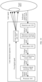
- FIG. 10 is an example of a laser detection apparatus according to an embodiment of this application. A complete description of this embodiment of this application is made in the following based on FIG. 10 .
- the laser detection apparatus 1000 shown in FIG. 10 includes a detection unit 1001, an optical-to-electrical conversion unit 1002, a shunt circuit 1003, an analog-to-digital converter 1004, a processor 1005, a signal conditioning circuit 1006, and a laser transmit unit 1007.
- An output end of the detection unit 1001 is connected to an input end of the optical-to-electrical conversion unit 1002.
- An output end of the optical-to-electrical conversion unit 1002 is connected to an input end of the shunt circuit 1003.
- An output end of the shunt circuit 1003 is connected to an input end of the signal conditioning circuit 1006.
- An output end of the signal conditioning circuit 1006 is connected to an input end of the analog-to-digital converter 1004.
- An output end of the analog-to-digital converter 1004 is connected to the processor 1005.
- the processor 1005 is connected to the laser transmit unit 1007.
- the processor 1005 may send a first digital signal to the laser transmit unit 1007, and the laser transmit unit 1007 may transmit a laser signal to a target object under driving of the first digital signal.
- the detection unit 1001 may detect an optical signal reflected by the target object, and input the optical signal to the optical-to-electrical conversion unit 1002.
- the optical-to-electrical conversion unit 1002 may be configured to perform optical-to-electrical conversion on the received optical signal to obtain a current signal, and input the current signal to the shunt circuit 1003.
- the current signal includes a first current signal and a third current signal.
- the shunt circuit 1003 may shunt the first current signal to obtain N second current signals, and generate N second voltage signals based on the N second current signals.
- the shunt circuit 1003 may shunt the third current signal to obtain the third current signal, and determine a first voltage signal based on the third current signal.
- the shunt circuit 1003 inputs the first voltage signal and the N second voltage signals to the analog-to-digital converter 1004.
- the analog-to-digital converter 1004 converts the first voltage signal and the N second voltage signals to obtain a second digital signal, and inputs the second digital signal to the processor 1005.
- the processor 1005 may determine information about a distance between the target object and the laser detection apparatus 1000 and intensity information of a reflected signal based on the second digital signal.
- the shunt circuit 1003 may shunt the first current signal to generate one or more second voltage signals, so that voltage signals corresponding to optical signals with a high luminous intensity detected by the detection apparatus are not saturated. In this way, the detection apparatus may accurately calculate the distance between the target object and the detection apparatus and the intensity information of the optical signal, and a luminous intensity range of reflected signals that can be detected by the detection apparatus is effectively increased.
- connection in this embodiment of this application may be a direct connection.
- connection may not be a direct connection, but may be performed by using some components. This is not limited in this embodiment of this application.
- An embodiment of this application further provides a sensor system.
- the sensor system includes one or more of the foregoing detection apparatuses.
- the sensor system may further include one or more of a millimeter-wave radar, a camera apparatus, and the like. There may be one or more millimeter-wave radars, and there may also be one or more camera apparatuses.
- An embodiment of this application further provides a vehicle.
- the vehicle carries the foregoing sensor system.
- the vehicle may further include a braking system, a control system, and the like.
- the sensor system is configured to detect a distance between the vehicle and another object.
- the control system is configured to send a control instruction based on a distance detected by the sensor system.
- the braking system is configured to execute the control instruction sent by the control system.
- An embodiment of this application further provides an uncrewed aerial vehicle device.
- the uncrewed aerial vehicle device carries the foregoing sensor system.
- the uncrewed aerial vehicle device may further include a braking system, a control system, and the like.
- the sensor system is configured to detect a distance between the uncrewed aerial vehicle device and another object.
- the control system is configured to send a control instruction based on a distance detected by the sensor system.
- the braking system is configured to execute the control instruction sent by the control system.
- this application may be provided as a method, a system, or a computer program product. Therefore, this application may use a form of a hardware-only embodiment, a software-only embodiment, or an embodiment with a combination of software and hardware. In addition, this application may use a form of a computer program product implemented on one or more computer-usable storage media (including but not limited to a disk memory, a CD-ROM, an optical memory, and the like) that include computer-usable program code.
- a computer-usable storage media including but not limited to a disk memory, a CD-ROM, an optical memory, and the like
- These computer program instructions may be stored in a computer-readable memory that can instruct the computer or any other programmable data processing device to work in a specific manner, so that the instructions stored in the computer-readable memory generate an artifact that includes an instruction apparatus.
- the instruction apparatus implements a specific function in one or more processes in the flowcharts and/or in one or more blocks in the block diagrams.
- These computer program instructions may also be loaded onto a computer or another programmable data processing device, so that a series of operations and steps are performed on the computer or the another programmable device, thereby generating computer-implemented processing. Therefore, the instructions executed on the computer or the another programmable device provide steps for implementing a specific function in one or more processes in the flowcharts and/or in one or more blocks in the block diagrams.
Landscapes
- Engineering & Computer Science (AREA)
- Physics & Mathematics (AREA)
- Computer Networks & Wireless Communication (AREA)
- General Physics & Mathematics (AREA)
- Radar, Positioning & Navigation (AREA)
- Remote Sensing (AREA)
- Electromagnetism (AREA)
- Optical Radar Systems And Details Thereof (AREA)
- Measurement Of Optical Distance (AREA)
Abstract
Description
- This application relates to the field of lidar technologies, and in particular, to a detection apparatus, a shunt circuit, and a terminal device.
- With the development of science and technology, laser ranging, microwave radar ranging, ultrasonic ranging, and the like have emerged in the field of ranging. A laser detection apparatus mainly includes a laser transmitter, a laser receiver, and a processor. The laser transmitter may transmit a laser signal. The laser signal is reflected after encountering an object. In this case, the laser receiver can detect the reflected signal, convert the reflected signal into an electrical signal, and perform corresponding processing (for example, amplification or conversion) on the electrical signal and output the electrical signal to the processor. In this way, the processor can determine a distance between the laser detection apparatus and the object and luminous intensity information of the reflected signal.
- However, if a luminous intensity of the reflected signal is high (for example, the luminous intensity exceeds 5,000 cd), the electrical signal obtained by the laser receiver through conversion of the reflected signal exceeds a range of signals that can be received by the processor, and the processor cannot accurately obtain the electrical signal corresponding to the reflected signal. Consequently, the processor cannot accurately determine the distance between the laser detection apparatus and the object and the luminous intensity information of the reflected signal. Therefore, a luminous intensity range of reflected signals that can be detected by the laser detection apparatus is limited.
- Therefore, how to improve the luminous intensity range (which may also be referred to as a dynamic range) of the reflected signals that can be detected by the laser detection apparatus is a technical problem to be resolved urgently.
- Embodiments of this application provide a detection apparatus, a shunt circuit, and a terminal device, to improve a luminous intensity range of reflected signals that can be detected by the detection apparatus. The method may be applied to the Internet of vehicles, for example, vehicle-to-everything (vehicle-to-everything, V2X), a long term evolution-vehicle (long term evolution-vehicle, LTE-V) technology, and vehicle to vehicle (vehicle-vehicle, V2V).
- According to a first aspect, an embodiment of this application provides a detection apparatus.
- For example, the detection apparatus may include a detection unit, an optical-to-electrical conversion unit, and a shunt circuit. The detection unit may be configured to receive an optical signal including a reflected signal of a laser transmit signal. The optical-to-electrical conversion unit may be configured to perform optical-to-electrical conversion on the received optical signal, to obtain a current signal including a first current signal. The shunt circuit may be configured to shunt the first current signal to obtain N second current signals used to generate N second voltage signals Vi. N is an integer greater than or equal to 1, and i is an integer greater than or equal to 1 and less than or equal to N.
- In this embodiment of this application, after the optical-to-electrical conversion unit in the detection apparatus performs optical-to-electrical conversion on the optical signal to obtain the current signal, the shunt circuit may shunt the first current signal in the current signal, to obtain the N second current signals. The N second current signals may be used to generate a plurality of voltage signals, so that the detection apparatus may output a plurality of voltage signals. In this way, when the detection apparatus detects a reflected signal with a high luminous intensity, voltage signals obtained after the detection apparatus processes the current signal corresponding to the reflected signal are not saturated (namely, within a value range of voltage signals that can be received by a next-stage processing circuit), thereby effectively increasing a luminous intensity range of the reflected signals that can be detected by the detection apparatus.
- It should be noted that the "high luminous intensity" may be understood as that the luminous intensity of the current reflected signal exceeds the luminous intensity range of the reflected signals that can be detected by the detection apparatus. Different detection apparatuses may correspond to different luminous intensity ranges. For example, for a laser detection apparatus, a luminous intensity range is from 500 cd to 5,000 cd. For another example, for an infrared light detection apparatus, a luminous intensity range is from 100 cd to 1,000 cd.
- In a possible design, a current value of the current signal obtained by performing optical-to-electrical conversion on the optical signal by the optical-to-electrical conversion unit is greater than a preset threshold. In this design, the shunt circuit shunts the first current signal in the current signal only when the current value of the current signal corresponding to the reflected signal of a target object is greater than the preset threshold, to obtain a plurality of second current signals, and the plurality of second current signals may be used to generate a plurality of second voltage signals.
- In a possible design, the N second voltage signals Vi may be used to determine distance information of a target object generating the reflected signal and/or intensity information of the optical signal. In this design, because the N second voltage signals are not saturated, the distance information of the target object and/or the intensity information of the optical signal that are/is determined based on the N second voltage signals are/is more accurate.
- In a possible design, the shunt circuit may shunt the first current signal based on N preset first control signals, to obtain the N second current signals. One preset first control signal may correspond to one bias voltage, and the N preset first control signals correspond to N bias voltages VBi. Values of the N bias voltages may be the same or different. This is not specifically limited in this embodiment of this application.
- It should be noted that the N preset first control signals are in a one-to-one correspondence with the N second current signals. In other words, one second current signal may be obtained by shunting the first current signal based on one preset first control signal.
- In this design, the shunt circuit may shunt the first current signal based on the N preset first control signals, so that the shunt circuit can quickly shunt the first current signal, and a next-stage processing circuit can receive a voltage signal corresponding to the reflected signal more quickly, thereby effectively improving efficiency of determining information about a distance between the target object and the detection apparatus and/or the intensity information of the optical signal.
- In a possible design, the shunt circuit may include N second shunt circuits, and the N second shunt circuits may shunt the first current signal based on the N preset first control signals, to obtain the N second current signals.
- It should be noted that each of the N second shunt circuits is in a one-to-one correspondence with each of the N preset first control signals, and each first control signal is in a one-to-one correspondence with each of the N second current signals. In other words, each second shunt circuit may shunt the first current signal based on a first control signal corresponding to the second shunt circuit, to obtain one second current signal. For example, a
second shunt circuit 1 shunts the first current signal based on afirst control signal 1, to obtain a secondcurrent signal 1. For example, asecond shunt circuit 2 shunts the first current signal based on afirst control signal 2, to obtain a secondcurrent signal 2. - In this design, the N second shunt circuits that are in a one-to-one correspondence with the N preset first control signals are disposed in the shunt circuit, so that each second shunt circuit may shunt the first current signal based on the first control signal corresponding to the second shunt circuit, and each second shunt circuit may obtain a second current signal that meets a preset dynamic range (namely, a value range of the current signal) of the second shunt circuit.
- In a possible design, the shunt circuit may further shunt the first current signal based on received N second control signals, to obtain N fourth current signals used to generate N third voltage signals Vi'. One second control signal may correspond to one bias voltage, and the N second control signals correspond to N bias voltages VBi'. Values of the N bias voltages may be the same or different. This is not specifically limited in this embodiment of this application.
- It should be noted that the "received N second control signals" may be received by the shunt circuit from a next-stage processing circuit. The next-stage processing circuit may be an external processing circuit of the detection apparatus or an internal processing circuit of the detection apparatus. Optionally, the N second control signals may be dynamically determined based on the N second voltage signals output by the shunt circuit. For example, a
second control signal 1 is determined based on a second voltage signal V1, and asecond control signal 2 is determined based on asecond voltage signal 2. - In a possible design, the N third voltage signals Vi' may be used to determine the distance information of the target object generating the reflected signal and/or the intensity information of the optical signal. In this design, because the N third voltage signals are not saturated, the information about the distance between the target object and the detection apparatus and/or the intensity information of the optical signal that are/is determined based on the N third voltage signals Vi' are more accurate.
- In a possible design, the shunt circuit further includes a first shunt circuit, and the current signal further includes a third current signal. The first shunt circuit may be configured to shunt the third current signal used to generate a first voltage signal V0. In this design, the first shunt circuit shunts some current signals that are less than the preset threshold and that are in the current signal corresponding to the reflected signal, to obtain the third current signal, so that the some current signals can be quickly output.
- It should be noted that a current value corresponding to the third current signal is less than the preset threshold.
- In a possible design, the first voltage signal V0 may be used to determine the distance information of the target object generating the reflected signal and/or the intensity information of the optical signal. In this design, the first voltage signal generated based on the third current signal may be used to determine the distance information of the target object generating the reflected signal and/or the intensity information of the optical signal, so that the distance information of the target object and/or the intensity information of the optical signal that are/is determined by the detection apparatus are/is more accurate.
- According to a second aspect, an embodiment of this application further provides a shunt circuit. The shunt circuit may be a shunt circuit in the foregoing detection apparatus.
- For example, the shunt circuit may include a first node N1, N second shunt circuits, and N processing circuits. The first node N1 is coupled to input ends of the N second shunt circuits, and output ends of the N second shunt circuits are respectively coupled to input ends of the N processing circuits. N is an integer greater than or equal to 1. The first node N1 may be configured to input a first current signal to the N second shunt circuits. The N second shunt circuits may be configured to shunt the first current signal to obtain N second current signals. The N processing circuits may be configured to process the N second current signals to generate N second voltage signals Vi.
- In this embodiment of this application, the N second shunt circuits and the N processing circuits are disposed in the shunt circuit, so that each second shunt circuit may shunt the first current signal to obtain corresponding second current signals, and the processing circuits corresponding to the second shunt circuits may further process the second current signals to generate the second voltage signals. In this way, the shunt circuit may output a plurality of voltage signals, so that the voltage signals output by the shunt circuit are not saturated.
- In a possible design, the N second voltage signals may be used to determine distance information of a target object generating a reflected signal and/or intensity information of an optical signal. For a specific description and beneficial effects of the design, refer to the foregoing related descriptions in the second aspect.
- In a possible design, the shunt circuit may further include a first component and a first shunt circuit. An output end of the first component is coupled to an input end of the first shunt circuit, and the output end of the first component is coupled to input ends of the N second shunt circuits through the first node N1. The first component may be configured to obtain a current signal including the first current signal and a third current signal. The first shunt circuit may be configured to shunt the current signal to obtain the third current signal used to generate a first voltage signal V0.
- In this design, the first component configured to obtain the current signal is disposed, and the output end of the first component is coupled to both the input end of the first shunt circuit and the input ends of the N second shunt circuits, so that the current signal is shunted. In addition, the N second current signals and the third current signal that are obtained after shunting may generate a plurality of voltage signals, so that the voltage signals output by the shunt circuit are not saturated.
- In a possible design, the first voltage signal V0 may be used to determine the distance information of the target object generating the reflected signal and/or the intensity information of the optical signal. For a specific description and beneficial effects of the design, refer to the foregoing related descriptions in the second aspect.
- In a possible design, a current value of the current signal is greater than a preset threshold, and a current value of the third current signal is less than the preset threshold. For a specific description and beneficial effects of the design, refer to the foregoing related descriptions in the second aspect.
- In a possible design, the N second shunt circuits may shunt the first current signal based on the N preset first control signals, to obtain the N second current signals. For a specific description and beneficial effects of the design, refer to the foregoing related descriptions in the second aspect.
- In a possible design, the N processing circuits may be further configured to receive the N second control signals. The N second shunt circuits may be further configured to shunt the first current signal based on the N second control signals, to obtain N fourth current signals. The N processing circuits may be further configured to process the N fourth current signals, to obtain N third voltage signals Vi'. For a specific description and beneficial effects of the design, refer to the foregoing related descriptions in the second aspect.
- In a possible design, an ith second shunt circuit in the N second shunt circuits may include a discharge circuit Di. Each of the N processing circuits includes a first resistor Rsensor, a second node N2, a first capacitor C1, and an amplification circuit. An input end of the discharge circuit Di is coupled to the first node N1. The first resistor Rsensor is coupled to both an output end of the discharge circuit Di and an input end of the amplification circuit. One end of the first capacitor C1 is coupled to both the first resistor Rsensor and the input end of the amplification circuit through the second node N2, and the other end is grounded. The discharge circuit Di may be configured to shunt the first current signal, to obtain the second current signals. The first resistor Rsensor may be configured to convert the second current signals into fourth voltage signals, and input the fourth voltage signals to the amplification circuit. The amplification circuit may be configured to amplify the fourth voltage signals to obtain the second voltage signals Vi.
- In this design, specific implementations of the second shunt circuits and the processing circuits are provided. In addition, the processing circuits may convert the second current signals obtained by the discharge circuit through shunting into voltage signals, and further amplify and output the voltage signals. In this way, a next-stage processing circuit can capture an accurate voltage signal, so that the distance information of the target object and/or the intensity information of the optical signal that are/is determined are/is more accurate.
- In a possible design, the discharge circuit Di may be one of the following components: a diode, a metal-oxide-semiconductor (metal oxide semiconductor field effect transistor, MOS) field-effect transistor, or a transistor. In this design, the discharge circuit has many implementations, so that implementation of the discharge circuit is simplified and complexity of the circuit is reduced.
- It should be understood that the amplification circuit in the processing circuits has a plurality of implementations, including but not limited to the following:
- Implementation 1: The amplification circuit includes a first amplification circuit, and the first amplification circuit may be configured to amplify the fourth voltage signals, to obtain the second voltage signals Vi. The first amplification circuit may include a second amplifier T2, and the second amplifier T2 may include one or more amplifiers. This is not specifically limited in this embodiment of this application.
- In
Implementation 1, a structure of the amplification circuit is simple, and implementation complexity of the processing circuits is effectively reduced. - Implementation 2: The amplification circuit may include a logarithmic amplification circuit and a second amplification circuit. An input end of the logarithmic amplification circuit is coupled to the first resistor Rsensor, and an output end of the logarithmic amplification circuit may be coupled to an input end of the second amplification circuit. The logarithmic amplification circuit may be configured to amplify the fourth voltage signals to obtain fifth voltage signals. The second amplification circuit may be configured to amplify the fifth voltage signals to obtain the second voltage signals Vi.
- In
Implementation 2, the logarithmic amplification circuit and the second amplification circuit are designed in the amplification circuit, so that a dynamic range (namely, a range of an output voltage) of the amplification circuit is effectively increased, and the second voltage signals output by the processing circuits can be more easily captured by a next-stage processing circuit. - In a possible design, the logarithmic amplification circuit may include a second amplifier T2, a second resistor R1, an equivalent diode D3, a third node N3, and a second capacitor C2. The second amplification circuit includes a third amplifier T3. One end of the second resistor R1 is coupled to an output end of the second amplifier T2, and the other end is coupled to both an input end of the equivalent diode D3 and an input end of the third amplifier T3. One end of the second capacitor C2 is coupled to an output end of the equivalent diode D3 through the third node N3, and the other end is grounded.
- In this design, after performing logarithmic amplification on the voltage signals obtained by converting the second current signals, the second amplifier T2 outputs the voltage signals to the third amplifier T3, so that the third amplifier T3 may further amplify the voltage signals obtained after the logarithmic amplification, to obtain the second voltage signals corresponding to the second current signals.
- In a possible design, the equivalent diode D3 may be any one of the diode, the MOS transistor, or the transistor. In this design, the equivalent diode D3 has a plurality of implementations, and complexity of the logarithmic amplification circuit is effectively reduced.
- In a possible design, the first component is an optical-to-electrical converter, and the first component may be further configured to receive an optical signal and convert the optical signal into a current signal. In this design, the first component has a function of optical-to-electrical signal conversion, so that the shunt circuit can shunt the current signal corresponding to the optical signal reflected by the target object.
- In a possible design, the first shunt circuit may include a first amplifier T1. The first amplifier T1 may be configured to: convert the third current signal obtained by the first shunt circuit through shunting to obtain a corresponding voltage signal, and amplify the voltage signal to obtain the first voltage signal. In this design, the first amplifier T1 is disposed in the first shunt circuit, so that implementation of the first shunt circuit is simple.
- It should be noted that the first amplifier T1 may be one or more amplifiers. This is not specifically limited in this embodiment of this application.
- According to a third aspect, an embodiment of this application provides a terminal device, including the detection apparatus according to any one of the first aspect and the possible designs of the first aspect. For example, examples of some terminal devices include but are not limited to: a smart home device (such as a television, a robotic vacuum cleaner, a smart desk lamp, a speaker system, a smart lighting system, an electrical control system, home background music, a home theater system, an intercom system, or video surveillance), an intelligent transportation device (such as a vehicle, a ship, an uncrewed aerial vehicle, a train, a wagon, or a truck), an intelligent manufacturing device (such as a robot, an industrial device, intelligent logistics, or a smart factory), and an intelligent terminal (such as a mobile phone, a computer, a tablet computer, a palmtop computer, a desktop computer, a headset, a speaker, a wearable device, a vehicle-mounted device, a virtual reality device, or an augmented reality device).
- For beneficial effects of the third aspect, refer to technical effects that can be achieved by corresponding designs in the first aspect. Details are not described herein again.
-
-
FIG. 1 is a schematic diagram of a structure of a laser detection apparatus to which an embodiment of this application is applicable; -
FIG. 2 is a schematic diagram of a structure of a laser receiver to which an embodiment of this application is applicable; -
FIG. 3 is a schematic diagram of a structure of a detection apparatus according to an embodiment of this application; -
FIG. 4A is a schematic diagram of a possible structure of a shunt circuit according to an embodiment of this application; -
FIG. 4B is a schematic diagram of another possible structure of a shunt circuit according to an embodiment of this application; -
FIG. 4C is a schematic diagram of another possible structure of a shunt circuit according to an embodiment of this application; -
FIG. 5A is a possible schematic diagram 1 of a shunt circuit according to an embodiment of this application; -
FIG. 5B is a possible schematic diagram 2 of a shunt circuit according to an embodiment of this application; -
FIG. 6 is a possible schematic diagram 3 of a shunt circuit according to an embodiment of this application; -
FIG. 7 is a possible schematic diagram 4 of a shunt circuit according to an embodiment of this application; -
FIG. 8 is a schematic diagram of a structure of another detection apparatus according to an embodiment of this application; -
FIG. 9 is a schematic diagram of a structure of still another detection apparatus according to an embodiment of this application; and -
FIG. 10 is a schematic diagram of a structure of yet another detection apparatus according to an embodiment of this application. - The following clearly and completely describes the technical solutions in embodiments of this application with reference to the accompanying drawings in embodiments of this application.
- It should be understood that in the following descriptions of embodiments of this application, "a plurality of" may be understood as "at least two". "And/or" describes an association relationship between associated objects, and represents that three relationships may exist. For example, A and/or B may represent the following cases: Only A exists, both A and B exist, and only B exists, where A and B may be singular or plural. Terms such as "first", "second" and "third" are merely used for distinction and description, and shall not be understood as an indication or implication of relative importance or an indication or implication of an order. For example, a "first control signal" and a "second control signal" mentioned below are merely used to indicate different control signals, and do not have different sequences, priorities, or importance degrees.
- Before the technical solutions provided in embodiments of this application are described in detail, an application scenario in embodiments of this application is first described.
- Currently, in many scenarios, a detection apparatus may be used to detect a distance of a target object. For example, with reference to
FIG. 1 , a laser detection apparatus 100 is used as an example of the detection apparatus. The laser detection apparatus 100 may include alaser transmitter 1, alaser receiver 2, and aprocessing circuit 3. - The
laser transmitter 1 may transmit a laser signal. After receiving the laser signal, atarget object 4 reflects a corresponding optical signal (namely, a reflected signal). Thelaser receiver 2 may detect the reflected signal reflected by thetarget object 4, convert the reflected signal to obtain a corresponding voltage signal, and input the voltage signal to theprocessing circuit 3. Theprocessing circuit 3 may determine a distance between thetarget object 4 and the laser detection apparatus 100 and intensity information of the reflected signal based on the voltage signal. -
FIG. 2 is a possible schematic diagram of a structure of thelaser receiver 2. InFIG. 2 , Vcc is an optical signal input end of thelaser receiver 2, Vbias is a control signal input end of thelaser receiver 2, and Vout is an output end of thelaser receiver 2. Thelaser receiver 2 includes an optical-to-electrical converter 201 and anamplification circuit 202. - The optical-to-electrical converter 201 may convert an optical signal received from the input end Vcc of the
laser receiver 2, to obtain a current signal, and input the current signal to theamplification circuit 202. - The
amplification circuit 202 includes an amplifier T0 and a resistor R0. The amplifier T0 may convert, based on a control signal input by the control signal input end Vbias, the current signal to obtain avoltage signal 1, amplify thevoltage signal 1 to obtain avoltage signal 2, and output thevoltage signal 2 through the output end Vout. - In a possible implementation, the
amplification circuit 202 may output thevoltage signal 2 to theprocessing circuit 3. After receiving thevoltage signal 2, theprocessing circuit 3 may perform analog-to-digital conversion on thevoltage signal 2, to obtain a time at which the reflected signal is returned from thetarget object 4 to thelaser receiver 2, and then calculate a distance between thetarget object 4 and the laser detection apparatus 100 and intensity information of the reflected signal of thetarget object 4 based on the time. - However, when the distance between the
target object 4 and the laser detection apparatus 100 is too short or a reflected power of thetarget object 4 is too large, a luminous intensity of the reflected signal of the target object is high. Consequently, a voltage value of thevoltage signal 2 obtained by converting the reflected signal by thelaser receiver 2 exceeds a value range of voltage signals that can be received by the processing circuit 3 (namely, voltages output by thelaser receiver 2 are saturated), and theprocessing circuit 3 cannot accurately calculate the distance between thetarget object 4 and the laser detection apparatus 100, and the intensity information corresponding to the reflected signal. - Therefore, there is a technical problem to be resolved urgently: The voltages output by the
laser receiver 2 avoid being saturated, so that the laser detection apparatus 100 can accurately detect the distance of the target object and/or the intensity information of the reflected signal of the target object, to increase a detection range of the laser detection apparatus. - In view of this, an embodiment of this application provides a detection apparatus. The detection apparatus includes a detection unit, an optical-to-electrical conversion unit, and a shunt circuit. The detection unit may be configured to receive an optical signal including a reflected signal of a laser transmit signal. The optical-to-electrical conversion unit may be configured to perform optical-to-electrical conversion on the received optical signal, to obtain a current signal including a first current signal. The shunt circuit may be configured to shunt the first current signal to obtain N second current signals used to generate N second voltage signals Vi. N is an integer greater than or equal to 1, and i is an integer greater than or equal to 1 and less than or equal to N.
- In this embodiment of this application, the shunt circuit is disposed in the detection apparatus. The shunt circuit may shunt the first current signal, to obtain the N second current signals. Each second current signal may generate one voltage signal, so that the detection apparatus may output a plurality of voltage signals. In this way, when the detection apparatus detects a reflected signal with a high luminous intensity, voltage signals obtained after the detection apparatus processes the current signal corresponding to the reflected signal are not saturated (namely, within a value range of voltage signals that can be received by a next-stage processing circuit), thereby effectively increasing a luminous intensity range of reflected signals that can be detected by the detection apparatus.
- It should be noted that, the "reflected signal with a high luminous intensity" may be understood as that the luminous intensity of the current reflected signal exceeds the luminous intensity range of the reflected signals that can be detected by the detection apparatus. It should be understood that a laser includes infrared light, ultraviolet light, and the like. Correspondingly, different laser detection apparatuses can detect reflected signals of different luminous intensity ranges. For example, a luminous intensity range of reflected signals that can be detected by an infrared light detection apparatus is from 500 cd to 5,000 cd. For another example, a luminous intensity range of reflected signals that can be detected by an ultraviolet light detection apparatus is from 100 cd to 1,000 cd.
- The following describes an application scenario of the detection apparatus provided in this embodiment of this application with reference to specific examples.
- In a possible implementation, the detection apparatus may be a laser detection apparatus. For example, for a vehicle having an autonomous driving mode or an assisted driving mode, the laser detection apparatus may be mounted on the vehicle. In this way, in a traveling process of the vehicle, the laser detection apparatus may detect a laser signal reflected by a target object. The laser detection apparatus can determine a current signal corresponding to the laser signal, shunt the current signal to obtain a plurality of current signals, and process the plurality of current signals to obtain a plurality of voltage signals. In this way, the laser detection apparatus can output a plurality of voltage signals, so that the voltage signals output by the laser detection apparatus are not saturated. Therefore, when detecting a reflected signal with a high luminous intensity, the laser detection apparatus can also accurately obtain information about a distance between the target object and the laser detection apparatus and/or intensity information of the laser signal reflected by the target object, thereby effectively increasing a luminous intensity range of reflected signals that can be detected by the laser detection apparatus, and further determining more obstacles on a pavement by the laser detection apparatus. In this way, the vehicle can optimize a traveling trajectory of the vehicle, thereby effectively improving safety of autonomous driving or assisted driving.
- Further, if the laser detection apparatus is an infrared light detection apparatus, the laser detection apparatus may further have another application scenario. For example, for an uncrewed aerial vehicle, the infrared light detection apparatus may be mounted on the uncrewed aerial vehicle. In this way, in a flight process of the uncrewed aerial vehicle, the infrared light detection apparatus may detect an infrared light signal reflected by a target object. The infrared light detection apparatus shunts a current signal generated by the infrared light signal, to obtain a plurality of current signals, thereby generating a plurality of voltage signals and effectively avoiding voltage signals output by the infrared light detection apparatus from being saturated. In this case, the infrared light detection apparatus can accurately determine a distance between the target object and the infrared light detection apparatus based on the infrared light signal, so that when the uncrewed aerial vehicle enters a danger range (that is, the target object in the danger range is detected), an alarm may be generated for the uncrewed aerial vehicle.
- It should be understood that the laser detection apparatus may also be an ultraviolet light detection apparatus, a visible light detection apparatus, or the like. Examples are not described herein again.
- It should be noted that the detection apparatus disclosed in this embodiment of this application may be applied to a terminal device having a signal processing capability. In some embodiments of this application, the detection apparatus may be a terminal device or an independent unit. When the detection apparatus is an independent unit, the unit may be embedded in a terminal device. In this way, when the detection apparatus detects a reflected signal with a large luminous intensity, the terminal device may shunt a current signal corresponding to the reflected signal, so that voltage signals output by the detection apparatus are not saturated (namely, within a value range of voltage signals that can be received by a next-stage processing circuit), thereby effectively increasing a luminous intensity range of reflected signals that can be detected by the detection apparatus. The terminal device may be an intelligent device having a signal processing capability, including but not limited to: a smart home device, such as a television, a robotic vacuum cleaner, a smart desk lamp, a speaker system, an intelligent lighting system, an electrical control system, home background music, a home theater system, an intercom system, or video surveillance; an intelligent transportation device, such as a vehicle, a ship, an uncrewed aerial vehicle, a train, a wagon, or a truck; and an intelligent manufacturing device, such as a robot or an industrial device. Alternatively, the terminal device may be a computer device having a signal processing capability, such as a desktop computer, a personal computer, or a server. It should be further understood that the terminal device may alternatively be a portable electronic device having a shunting capability, such as a mobile phone, a tablet computer, a palmtop computer, a headset, a speaker, a wearable device (such as a smart watch), a vehicle-mounted device, a virtual reality device, or an augmented reality device.
- The following describes a structure of the detection apparatus provided in this embodiment of this application with reference to specific accompanying drawings.
- It should be noted that "coupling" in the following embodiment of this application may be an electrical connection, and an electrical connection between two electrical elements may be a direct or indirect connection between the two electrical elements. For example, a connection between A and B may be either a direct connection between A and B, or an indirect connection between A and B through one or more other electrical elements. For example, the connection between A and B may be that A and C are directly connected, C and B are directly connected, and A and B are connected through C. In short, coupling between A and B enables electric energy to be transmitted between A and B.
- For example,
FIG. 3 is a schematic diagram of a circuit structure of a detection apparatus according to an embodiment of this application. As shown inFIG. 3 , the detection apparatus may include adetection unit 301, an optical-to-electrical conversion unit 302, and ashunt circuit 303. - An input end a1 of the
detection unit 301 is configured to receive an optical signal. An output end a2 of thedetection unit 301 is coupled to an input end b1 of the optical-to-electrical conversion unit 302, and is configured to input the received optical signal to the optical-to-electrical conversion unit 302. An output end b2 of the optical-to-electrical conversion unit 302 is coupled to an input end c1 of theshunt circuit 303. - In a possible implementation, the optical signal includes a reflected signal of a laser transmit signal. The optical-to-
electrical conversion unit 302 may be configured to perform optical-to-electrical conversion on the received optical signal to obtain acurrent signal 1, and input thecurrent signal 1 to theshunt circuit 303. Thecurrent signal 1 includes a first current signal. Theshunt circuit 303 may be configured to shunt the first current signal to obtain N second current signals used to generate N second voltage signals. N is an integer greater than or equal to 1. In this implementation, because theshunt circuit 303 may shunt the first current signal, one or more second voltage signals are generated, so that voltage signals corresponding to optical signals with a high luminous intensity detected by the detection apparatus are not saturated (namely, within a value range of voltage signals that can be received by a next-stage processing circuit), and a luminous intensity range of reflected signals that can be detected by the detection apparatus is effectively increased. - It should be noted that the
shunt circuit 303 shunts the first current signal in a plurality of implementations, including but not limited to the following: - Manner 1: The
shunt circuit 303 may shunt the first current signal based on N preset first control signals to obtain N second current signals used to generate N second voltage signals Vi. - It should be noted that "each preset first control signal" corresponds to a preset bias voltage, and the preset bias voltage is a bias voltage preconfigured in the
shunt circuit 303 when technical personnel design theshunt circuit 303. A quantity of N is not specifically limited in this embodiment of this application. - For example, N is 4, and the
shunt circuit 303 may shunt the first current signal based on four preset first control signals to obtain four second current signals, and then may obtain four second voltage signals V1, V2, V3, and V4 based on the four current signals. - It may be understood that the N preset first control signals are in a one-to-one correspondence with the N second current signals. In other words, one second current signal may be obtained by shunting the first current signal based on a bias voltage corresponding to one first control signal. For example, if a
first control signal 1 corresponds to a bias voltage VB1, theshunt circuit 303 may shunt the first current signal based on the bias voltage VB1, to obtain a secondcurrent signal 1. For another example, if afirst control signal 2 corresponds to a bias voltage VB2, theshunt circuit 303 may shunt the first current signal based on the bias voltage VB2, to obtain a secondcurrent signal 2. For still another example, if afirst control signal 3 corresponds to a bias voltage VB3, theshunt circuit 303 may shunt the first current signal based on the bias voltage VB3, to obtain a secondcurrent signal 3. - In
Manner 1, theshunt circuit 303 directly shunts the first current signal based on the preset first control signals, thereby effectively improving shunting efficiency of theshunt circuit 303. - Manner 2: The
shunt circuit 303 may shunt the first current signal based on N preset first control signals to obtain N second current signals used to generate N second voltage signals Vi. Then, theshunt circuit 303 further shunts the first current signal based on received N second control signals to obtain N fourth current signals used to generate N third voltage signals Vi'. - It should be noted that the "received N second control signals" may be received by the
shunt circuit 303 from a next-stage processing circuit. The next-stage processing circuit may be an external processing circuit of the detection apparatus 300 or an internal processing circuit of the detection apparatus 300. One received second control signal may correspond to one bias voltage VBi', and received N second control signals correspond to N bias voltages. Current values corresponding to the N second current signals are different from current values corresponding to the fourth current signals, and voltage values corresponding to the N second voltage signals are different from voltage values corresponding to the N third voltage signals. - It may be understood that the received N second control signals are in a one-to-one correspondence with the N fourth current signals. In other words, one fourth current signal may be obtained by shunting the first current signal based on a bias voltage corresponding to one second control signal. For example, if a
second control signal 1 corresponds to a bias voltage VB1', theshunt circuit 303 may shunt the first current signal based on the bias voltage VB1', to obtain a fourthcurrent signal 1. For another example, if asecond control signal 2 corresponds to a bias voltage VB2', theshunt circuit 303 may shunt the first current signal based on the bias voltage VB2', to obtain a fourthcurrent signal 2. For still another example, if asecond control signal 3 corresponds to a bias voltage VB3', theshunt circuit 303 may shunt the first current signal based on the bias voltage VB3', to obtain a fourthcurrent signal 3. For descriptions of the first control signal, refer to related descriptions inManner 1. - The N second control signals are determined after the N first control signals are determined.
- In a possible implementation, after obtaining the N second current signals based on the N first control signals, the
shunt circuit 303 may convert the N second current signals into the N second voltage signals, and output the N second voltage signals to a next-stage processing circuit. The next-stage processing circuit may determine the N bias voltages corresponding to the N second control signals based on the N second voltage signals. A larger voltage value corresponding to the second voltage signal indicates a larger bias voltage value that is corresponding to the second control signal and that is set by the next-stage processing circuit. - For example, there is a mapping relationship between the voltage value corresponding to the second voltage signal and the bias voltage value corresponding to the second control signal, as shown in Table 1. The next-stage processing circuit may determine the bias voltage value corresponding to the second control signal based on the mapping relationship. For example, if a voltage value corresponding to a
second voltage signal 1 is 80 V, a bias voltage corresponding to asecond control signal 1 is 75 V; if a voltage value corresponding to asecond voltage signal 2 is 50 V, a bias voltage corresponding to asecond control signal 2 is 55 V; and if a voltage value corresponding to asecond voltage signal 3 is 30 V, a bias voltage corresponding to asecond control signal 3 is 35 VTable 1 Voltage value (v) corresponding to a second voltage signal Bias voltage value (v) corresponding to a second control signal 80 75 50 55 30 35 - It may be understood that the mapping relationship in Table 1 is merely an example, and is not limited. More mapping relationships may exist between the voltage value corresponding to the second voltage signal and the bias voltage value corresponding to the second control signal, provided that the voltage value corresponding to the second voltage signal is directly proportional to the bias voltage value corresponding to the second control signal.
- The following describes the technical solution of
Manner 2 with reference to a complete example. - For example,
FIG. 4A is a schematic diagram of a possible structure of ashunt circuit 303. For example, N is 4, and theshunt circuit 303 inFIG. 4A includes a first subcircuit and a second subcircuit. As shown in (a) inFIG. 4A , the first subcircuit in theshunt circuit 303 may receive acurrent signal 1, shunt a first current signal in thecurrent signal 1 based on four preset first control signals to obtain four second current signals, and input the four second current signals to the second subcircuit in theshunt circuit 303. The second subcircuit in theshunt circuit 303 obtains four second voltage signals, V1, V2, V3, and V4, based on the four second current signals, and inputs the four second voltage signals to a next-stage processing circuit. The next-stage processing circuit determines four second control signals based on the four second voltage signals and mapping relationships between voltage values corresponding to the second voltage signals and bias voltage values corresponding to the second control signals, and inputs the four second control signals to the first subcircuit in theshunt circuit 303. As shown in (b) inFIG. 4A , the first subcircuit in theshunt circuit 303 may shunt the first current signal again based on the four second control signals to obtain four fourth current signals, and input the four fourth current signals to the second subcircuit in theshunt circuit 303. The second sub circuit in theshunt circuit 303 obtains four third voltage signals, V1', V2', V3', and V4' based on the four second current signals, and inputs the four third voltage signals to the next-stage processing circuit. - In
Manner 2, after shunting the first current signal based on the N preset first control signals to obtain the N second current signals, and converting the N second current signals into the N second voltage signals, theshunt circuit 303 may further shunt the first current signal again based on the N second control signals, to obtain the N fourth current signals. The N second control signals are dynamically determined based on the N second voltage signals, so that the third voltage signals determined based on the fourth current signals obtained through shunting can better adapt to a voltage receiving range of a next-stage processing circuit. - It should be understood that the N second voltage signals or the N third voltage signals may be used to determine distance information of a target object generating a reflected signal and/or intensity information of an optical signal.
- The following describes an implementation of the
shunt circuit 303 with reference to a specific example. -
FIG. 4B is a schematic diagram of a possible structure of ashunt circuit 303. InFIG. 4B , theshunt circuit 303 may include: a first node N1, N second shunt circuits (namely,second shunt circuits 1 to N), and N processing circuits (namely, aprocessing circuit 1, aprocessing circuit 2, ..., and a processing circuit N). The first node N1 is coupled to each input end of the N second shunt circuits, and output ends of the N second shunt circuits are respectively coupled to input ends of the N processing circuits. N is an integer greater than or equal to 1. - It should be understood that the first node N1 is an electrical node formed by connecting the N second shunt circuits, and is a connection point of the N second shunt circuits in actual hardware. The first node N1 may be configured to input a first current signal to the N second shunt circuits, and then each of the N second shunt circuits may shunt the first current signal to obtain N second current signals. Each second shunt circuit may input the second current signal obtained through shunting to a processing circuit corresponding to the second shunt circuit, and then the processing circuit may process the second current signal to generate a second voltage signal. Correspondingly, the N processing circuits may process the N second current signals to obtain N second voltage signals.
- It should be understood that the N second shunt circuits may be in a one-to-one correspondence with the N processing circuits. For example, a
second shunt circuit 1 corresponds to aprocessing circuit 1, asecond shunt circuit 2 corresponds to aprocessing circuit 2, and by analogy, a second shunt circuit N corresponds to a processing circuit N. - For example, the
second shunt circuit 1 may shunt the first current signal to obtain a second current signal I1, and input the second current signal I1 to the correspondingprocessing circuit 1, and then theprocessing circuit 1 may process the second current signal I1 to generate a second voltage signal V1. - For another example, the
second shunt circuit 2 may shunt the first current signal to obtain a second current signal I2, and input the second current signal I2 to the correspondingprocessing circuit 2, and then theprocessing circuit 2 may process the second current signal I2 to generate a second voltage signal V2. - For still another example, the second shunt circuit N may shunt the first current signal to obtain a second current signal In, and input the second current signal In to the corresponding processing circuit N, and then the processing circuit N may process the second current signal In to generate a second voltage signal VN.
- As shown in
FIG. 4B , theprocessing circuit 1 to the processing circuit N further include control signal input ends VB1 to VBN. Theprocessing circuit 1 to the processing circuit N may input corresponding control signals into the N second shunt circuits, and then the N second shunt circuits may shunt the first current based on the control signals. - Correspondingly, the N second shunt circuits shunt the first current signal in a plurality of implementations, including but not limited to the following:
Manner 1: The N second shunt circuits may shunt the first current signal based on N preset first control signals to obtain N second current signals used to generate N second voltage signals. - It should be noted that the N second shunt circuits are in a one-to-one correspondence with the N preset first control signals, and the N preset first control signals are in a one-to-one correspondence with the N second current signals. In other words, one second shunt circuit may shunt the first current signal based on a bias voltage corresponding to one first control signal, to obtain one second current signal.
- For example, a
second shunt circuit 1 may shunt the first current signal based on a bias voltage VB1 corresponding to afirst control signal 1, to obtain a secondcurrent signal 1. For another example, asecond shunt circuit 2 may shunt the first current signal based on a bias voltage VB2 corresponding to afirst control signal 2, to obtain a secondcurrent signal 2. For still another example, asecond shunt circuit 3 may shunt the first current signal based on a bias voltage VB3 corresponding to afirst control signal 3, to obtain a secondcurrent signal 3. - One preset first control signal may correspond to one preset bias voltage, and the N preset first control signals correspond to N preset bias voltages. Values of the N preset bias voltages may be the same or different. This is not specifically limited in this embodiment of this application.
- For example, values of a
bias voltage 1 to a bias voltage N may all be 5 V Alternatively, values of abias voltage 1 to abias voltage 3 are 5 V, and values of abias voltage 4 to a bias voltage Nare 10 V. - Optionally, a value of an Nth bias voltage among the N bias voltages may be twice a value of an (N+1)th bias voltage.
- For example, N is 1, 2, or 3. A value of the bias voltage VB1 corresponding to the
first control signal 1 is 20 V, a value of the bias voltage VB2 corresponding to thefirst control signal 2 is 10 V, and a value of the bias voltage VB3 corresponding to thefirst control signal 3 is 5 V - In
Manner 1, the N second shunt circuits directly shunt the first current signal based on the preset first control signals, thereby effectively improving shunting efficiency of the N second shunt circuits. - Manner 2: The N second shunt circuits may shunt the first current signal based on N preset first control signals to obtain N second current signals used to generate N second voltage signals. Then, the N second shunt circuit further shunt the first current signal based on received N second control signals to obtain N fourth current signals used to generate N third voltage signals Vi'.
- It may be understood that the N second shunt circuits are in a one-to-one correspondence with the received N second control signals, and the received N first control signals are in a one-to-one correspondence with the N fourth current signals. In other words, one second shunt circuit may shunt the first current signal based on a bias voltage corresponding to one second control signal, to obtain one fourth current signal. For example, a
second shunt circuit 1 may shunt the first current signal based on a bias voltage VB1 corresponding to asecond control signal 1, to obtain a fourthcurrent signal 1. For another example, asecond shunt circuit 2 may shunt the first current signal based on a bias voltage VB2 corresponding to asecond control signal 2, to obtain a fourthcurrent signal 2. For still another example, asecond shunt circuit 3 may shunt the first current signal based on a bias voltage VB3 corresponding to asecond control signal 3, to obtain a fourthcurrent signal 3. - It can be learned from the foregoing descriptions that a next-stage processing circuit may determine the N bias voltages corresponding to the N second control signals based on the N second voltage signals output by the
shunt circuit 303. Correspondingly, the next-stage processing circuit may determine the N bias voltages corresponding to the N second control signals based on the N second voltage signals output by the N second shunt circuits. A larger voltage value corresponding to the second voltage signal indicates a larger bias voltage value that is corresponding to the second control signal and that is set by the next-stage processing circuit. - The following describes the technical solution of
Manner 2 with reference to a specific example. - For example, with reference to
FIG. 4C , N is 3, and ashunt circuit 303 includes asecond shunt circuit 1, asecond shunt circuit 2, asecond shunt circuit 3, aprocessing circuit 1, aprocessing circuit 2, and aprocessing circuit 3. The first node N1 inputs a first current signal to each of thesecond shunt circuit 1, thesecond shunt circuit 2, and thesecond shunt circuit 3. Thesecond shunt circuit 1 shunts the first current signal based on a bias voltage VB1 corresponding to a presetfirst control signal 1 to obtain a secondcurrent signal 1, and inputs the secondcurrent signal 1 to theprocessing circuit 1, and then theprocessing circuit 1 generates a second voltage signal V1 based on the secondcurrent signal 1, and inputs the second voltage signal V1 to a next-stage processing circuit. Thesecond shunt circuit 2 shunts the first current signal based on a bias voltage VB2 corresponding to a presetfirst control signal 2 to obtain a secondcurrent signal 2, and inputs the secondcurrent signal 2 to theprocessing circuit 2, and then theprocessing circuit 2 generates a second voltage signal V2 based on the secondcurrent signal 2, and inputs the second voltage signal V2 to a next-stage processing circuit. Thesecond shunt circuit 3 shunts the first current signal based on a bias voltage VB3 corresponding to a presetfirst control signal 3 to obtain a secondcurrent signal 3, and inputs the secondcurrent signal 3 to theprocessing circuit 3, and then theprocessing circuit 3 generates a second voltage signal V3 based on the secondcurrent signal 3, and inputs the second voltage signal V3 to a next-stage processing circuit. - The next-stage processing circuit determines a
second control signal 1, asecond control signal 2, and asecond control signal 3 according to the second voltage signal V1, the second voltage signal V2, and the second voltage signal V3. The next-stage processing circuit inputs thesecond control signal 1 to theprocessing circuit 1. Theprocessing circuit 1 converts thesecond control signal 1 into a corresponding voltage signal VB1', and inputs the voltage signal VB1' to thesecond shunt circuit 1. Then, thesecond shunt circuit 1 shunts the first current signal again based on the voltage signal VB1' to obtain a fourthcurrent signal 1, and inputs the fourthcurrent signal 1 to theprocessing circuit 1. Then, theprocessing circuit 1 generates a third voltage signal V1' based on the fourthcurrent signal 1, and inputs the third voltage signal V1' to a next-stage processing circuit. - The next-stage processing circuit inputs the
second control signal 2 to theprocessing circuit 2. Theprocessing circuit 2 converts thesecond control signal 2 into a corresponding voltage signal VB2', and inputs the voltage signal VB2' to thesecond shunt circuit 2. Then, thesecond shunt circuit 2 shunts the first current signal again based on the voltage signal VB2' to obtain a fourthcurrent signal 2, and inputs the fourthcurrent signal 2 to theprocessing circuit 2. Then, theprocessing circuit 2 generates a third voltage signal V2' based on the fourthcurrent signal 2, and inputs the third voltage signal V2' to a next-stage processing circuit. - The next-stage processing circuit inputs the
second control signal 3 to theprocessing circuit 3. Theprocessing circuit 3 converts thesecond control signal 3 into a corresponding voltage signal VB3', and inputs the voltage signal VB3' to thesecond shunt circuit 3. Then, thesecond shunt circuit 3 shunts the first current signal again based on the voltage signal VB3' to obtain a fourthcurrent signal 3, and inputs the fourthcurrent signal 3 to theprocessing circuit 3. Then, theprocessing circuit 3 generates a third voltage signal V3' based on the fourthcurrent signal 2, and inputs the third voltage signal V3' to a next-stage processing circuit. - In
Manner 2, each of the N second shunt circuits first shunts the first current signal based on the preset first control signals, and then shunts the first current signal again based on the second control signals. The second control signals are dynamically determined based on the second voltage signals output by the second shunt circuits corresponding to the second control signals, so that the second shunt circuits can shunt the first current signal again and perform a quasi-conversion operation to obtain the third voltage signals which better adapt to a voltage receiving range of a next-stage processing circuit. - Optionally, still with reference to
FIG. 4B , theshunt circuit 303 may further include afirst shunt circuit 3031 and afirst component 3032. Aninput end 32a of thefirst component 3032 may be configured to obtain thecurrent signal 1. Aninput end 31a of thefirst shunt circuit 3031 is coupled to anoutput end 32b of thefirst component 3032 through a first node N1. Then, thefirst shunt circuit 3031 may shunt a third current signal in the current signal to obtain the third current signal, convert the third current signal to obtain a first voltage signal V0, and output the first voltage signal V0 through anoutput end 31b of thefirst shunt circuit 3031. - In a possible implementation, the
input end 32a of thefirst component 3032 may be coupled to a power supply Vcc of a detection apparatus 300, and thecurrent signal 1 is obtained through the power supply Vcc. In another possible implementation, theinput end 32a of thefirst component 3032 may be further coupled to an output end b2 of an optical-to-electrical conversion unit 302, to receive thecurrent signal 1 from the optical-to-electrical conversion unit 302. - It should be understood that, when the
shunt circuit 303 may further include thefirst shunt circuit 3031 and thefirst component 3032, the first node N1 may further be an electrical node formed by connecting the N second shunt circuits, thefirst shunt circuit 3031, and thefirst component 3032. In actual hardware, the first node N1 is a connection point of the N second shunt circuits, thefirst shunt circuit 3031, and thefirst component 3032. - In a possible implementation, a current value of the current signal is greater than a preset threshold, and a current value of the third current signal is less than the preset threshold. In other words, the
first shunt circuit 3031 shunts some current signals that are less than the preset threshold and that are in the current signal obtained by the first component, to obtain the third current signal, so that the some current signals can be quickly output. - In a possible implementation, the first voltage signal V0 may be used to determine distance information of a target object generating a reflected signal and/or intensity information of an optical signal. In this way, the distance information of the target object and/or the intensity information of the optical signal that are/is determined by the detection apparatus are/is more accurate.
- With reference to specific accompanying drawings, the following describes possible implementations of each part of the
shunt circuit 303. - In a possible implementation, the first shunt circuit may include a first amplifier. The first amplifier may be one or more amplifiers. That is, the first shunt circuit may include one or more amplifiers. This is not specifically limited in this embodiment of this application.
- For example, with reference to
FIG. 5A , an amplifier T1 inFIG. 5A is used as an example of the first amplifier. Thefirst shunt circuit 3031 includes the amplifier T1. An input end of the amplifier T1 is aninput end 31a of afirst shunt circuit 3031, and an output end of the amplifier T1 is anoutput end 31b of thefirst shunt circuit 3031. Then, the amplifier T1 may be configured to shunt a third current signal to obtain the third current signal, and convert the third current signal to obtain a first voltage signal V0. - For another example, with reference to
FIG. 5B , an amplifier T1 and an amplifier T11 inFIG. 5B are used as an example of the first amplifier. An input end of the amplifier T1 is aninput end 31a of afirst shunt circuit 3031, an output end of the amplifier T1 is coupled to an input end of the amplifier T11, and an output end of the amplifier T11 is anoutput end 31b of thefirst shunt circuit 3031. Then, the amplifier T1 may be configured to shunt a third current signal to obtain the third current signal, convert the third current signal to obtain acorresponding voltage signal 1, and input thevoltage signal 1 to the amplifier T11. The amplifier T11 amplifies thevoltage signal 1 again to obtain a first voltage signal V0. - It may be understood that the foregoing example is merely an example for describing the
first shunt circuit 3031. In another possible embodiment, there may be more amplifiers in thefirst shunt circuit 3031. - In a possible implementation, the
first component 3032 may be an optical-to-electrical converter D.An input end 32a of thefirst component 3032 is an input end of the optical-to-electrical converter D.An output end 32b of thefirst component 3032 is an output end of the optical-to-electrical converter D. Then, the optical-to-electrical converter D may receive an optical signal and convert the optical signal into the current signal. - For example, still with reference to
FIG. 5A orFIG. 5B , the input end of the optical-to-electrical converter D is configured to receive an optical signal (namely, a reflected signal of a target object), convert the optical signal into the current signal, input a first current signal in the current signal to asecond shunt circuit 1 through a first node N1, and input the third current signal in the current signal to the first shunt circuit through the first node N1. - It should be noted that, in some other embodiments, the
first component 3032 may alternatively be an acoustic-electric conversion component, a magneto-electric conversion component, or the like. - In a possible implementation, the N second shunt circuits may be implemented by using discharge circuits D1 to DN To be specific, the
second shunt circuit 1 may include a discharge circuit D1, asecond shunt circuit 2 may include a discharge circuit D2, asecond shunt circuit 3 may include a discharge circuit D3, ..., and so on, and the second shunt circuit N may include a discharge circuit DN. The discharge circuits D1 to DN may be implemented by using an equivalent diode. It may be understood that in embodiments of this application, the "equivalent diode" is a component having a conductive function of a diode. For example, the equivalent diode may be any one of a diode, a MOS transistor, or a transistor. This is not specifically limited in this embodiment of this application. - For example, still with reference to
FIG. 5A orFIG. 5B , a second shunt circuit is used as an example inFIG. 5A orFIG. 5B . Thesecond shunt circuit 1 may include an equivalent diode D1. An input end of the equivalent diode D1 is coupled to the first node N1, and an output end of the equivalent diode D1 is coupled to an input end of aprocessing circuit 1. Then, thesecond shunt circuit 1 may shunt the first current signal to obtain a second current signal, and input the second signal to theprocessing circuit 1. - It should be understood that the foregoing example is merely an example for describing the second shunt circuit, and does not constitute a limitation. In other embodiments, there may be more second shunt circuits. Correspondingly, specific implementations of other second shunt circuits are similar to a specific implementation of the
second shunt circuit 1, and details are not described herein again. - In a possible implementation, each of the N processing circuits may include a first resistor Rsensor, a second node N2, a first capacitor C1, and an amplification circuit.
- It should be understood that the second node N2 is an electrical node formed by connecting a control signal input end (VB1) of the processing circuit and an internal component of the processing circuit. In actual hardware, the second node N2 is a connection point of the component, for example, a connection point of the first resistor Rsensor, the first capacitor C1, and the amplification circuit.
- For example, still with reference to
FIG. 5A orFIG. 5B , theprocessing circuit 1 inFIG. 5A orFIG. 5B may include the first resistor Rsensor, the second node N2, the first capacitor C1, and theamplification circuit 3033. The first resistor Rsensor may convert a secondcurrent signal 1 received by the first resistor Rsensor from thesecond shunt circuit 1, to obtain a corresponding fourth voltage signal, and input the fourth voltage signal to theamplification circuit 3033. Theamplification circuit 3033 amplifies the fourth voltage signal to obtain a second voltage signal V1 and outputs the second voltage signal V1. - It should be understood that the foregoing example is merely an example for describing the processing circuit, and does not constitute a limitation. In other embodiments, there may be more second shunt circuits. Correspondingly, specific implementations of other processing circuits are similar to a specific implementation of the
processing circuit 1, and details are not described herein again. - It should be noted that the
amplification circuit 3033 has a plurality of implementations, including but not limited to the following:
Implementation 1: Theamplification circuit 3033 is implemented by using a first amplification circuit. - The first amplification circuit may include one or more amplifiers. In other words, the first amplification circuit may be a single-stage amplification circuit, or may be a multi-stage amplification circuit.
- For example, with reference to
FIG. 6 , a single-stage amplification circuit inFIG. 6 is used as an example of the first amplification circuit. That is, the first amplification circuit includes a second amplifier T2. That is, theamplification circuit 3033 is implemented by using the second amplifier T2. The second amplifier T2 may receive a fourth voltage signal from a first resistor Rsensor, amplify the fourth voltage signal to obtain a second voltage signal V1, and output the second voltage signal V1. - In
Implementation 1, a structure of theamplification circuit 3033 is simple, and implementation complexity of the processing circuits is effectively reduced. - Implementation 2: The
amplification circuit 3033 includes a logarithmic amplification circuit and a second amplification circuit. An input end of the logarithmic amplification circuit is coupled to the first resistor Rsensor, and an output end of the logarithmic amplification circuit is coupled to an input end of the second amplification circuit. The logarithmic amplification circuit is configured to amplify the fourth voltage signal to obtain a fifth voltage signal. The second amplification circuit may be configured to amplify the fifth voltage signal to obtain the second voltage signal V1. - For example, with reference to
FIG. 7 , the logarithmic amplification circuit may include a second amplifier T2, a second resistor R1, an equivalent diode D3, a third node N3, and a second capacitor C2. The second amplification circuit includes a third amplifier T3. One end of the second resistor R1 is coupled to an output end of the second amplifier T2, and the other end is coupled to both an input end of the equivalent diode D3 and an input end of the third amplifier T3. One end of the second capacitor C2 is coupled to an output end of the equivalent diode D3 through the third node N3, and the other end is grounded. In this way, the second amplifier T2 may perform logarithmic amplification on a fourth voltage signal output by the first resistor Rsensor to obtain a fifth voltage signal, and input the fifth voltage signal to the third amplifier T3. The third amplifier T3 may be configured to amplify the fifth voltage signal, to obtain a second voltage signal V1. - It should be understood that the third node N3 is an electrical node formed by connecting another control signal input end (VB1') of a
processing circuit 1 and an internal component of theprocessing circuit 1. In actual hardware, the third node N3 is a connection point of the component, for example, a connection point of the second capacitor C2, the equivalent diode D3, and the control signal input end (VB1'). The equivalent diode D3 is a component having a conducting function of a diode. For example, the equivalent diode D3 may be any one of a diode, a MOS transistor, or a transistor. This is not specifically limited in this embodiment of this application. - It should be understood that the foregoing example is merely an example for describing the logarithmic amplification circuit and the second amplification circuit, and does not constitute a limitation. In another embodiment, the logarithmic amplification circuit and the second amplification circuit may further include more amplifiers.
- In
Implementation 2, the logarithmic amplification circuit is designed in the amplification circuit, so that the amplification circuit can perform logarithmic amplification on the second voltage signal, thereby effectively improving a dynamic range (namely, a range of an output voltage) of the amplification circuit. - It should be noted that the
shunt circuit 303 may further be applied to another detection apparatus. This is merely an example, but not a limitation. - It should be noted that both the first voltage signal V0 and the second voltage signal V1 may be used to determine a distance signal of a target object and/or intensity information of a reflected signal of the target object.
- In some embodiments, as shown in
FIG. 8 , the detection apparatus 300 further includes an analog-to-digital converter 304 and aprocessor 305. An input end of the analog-to-digital converter 304 is connected to an output end of theshunt circuit 303, and an output end of the analog-to-digital converter 304 is connected to an input end of theprocessor 305. The analog-to-digital converter 304 is configured to convert a voltage signal (namely, the first voltage signal V0 and the second voltage signal V1) into a second digital signal, and output the second digital signal to theprocessor 305. Theprocessor 305 may determine distance information of a target object and/or intensity information of a reflected signal of the target object based on the second digital signal. - For example, the
processor 305 may obtain a moment at which a first digital electrical signal (a drive signal used when a transmit signal corresponding to the reflected signal is transmitted) starts to be output and a moment at which the second digital electrical signal starts to be received, and determine a first time difference between the two moments. The first time difference may be subtracted from a constant time spent in operating adetection unit 301, an optical-to-electrical conversion unit 302, theshunt circuit 303, and the analog-to-digital converter 30. In this way, a second time difference between a moment at which a laser signal is transmitted by a laser transmitter and a moment at which the detection apparatus 300 receives the reflected signal may be obtained. Then, theprocessor 305 may determine a distance between the laser detection apparatus and the target object and the luminous intensity information of the reflected signal based on the second time difference. - Optionally, the
processor 305 may determine the N second control signals based on the digital signal, and send the N second control signals to theshunt circuit 303, so that theshunt circuit 303 may shunt, based on the N second control signals, a current signal received from the optical-to-electrical conversion unit 302. - Optionally, with reference to
FIG. 9 , the detection apparatus 300 may further include a signal conditioning circuit 306, and the signal conditioning circuit 306 may be connected in series between theshunt circuit 303 and the analog-to-digital converter 304. In this way, the signal conditioning circuit 306 may filter out some interference signals in the voltage signals, so that the voltage signals received by the analog-to-digital converter 304 are more accurate. -
FIG. 10 is an example of a laser detection apparatus according to an embodiment of this application. A complete description of this embodiment of this application is made in the following based onFIG. 10 . - The laser detection apparatus 1000 shown in
FIG. 10 includes a detection unit 1001, an optical-to-electrical conversion unit 1002, a shunt circuit 1003, an analog-to-digital converter 1004, a processor 1005, a signal conditioning circuit 1006, and a laser transmitunit 1007. - An output end of the detection unit 1001 is connected to an input end of the optical-to-electrical conversion unit 1002. An output end of the optical-to-electrical conversion unit 1002 is connected to an input end of the shunt circuit 1003. An output end of the shunt circuit 1003 is connected to an input end of the signal conditioning circuit 1006. An output end of the signal conditioning circuit 1006 is connected to an input end of the analog-to-digital converter 1004. An output end of the analog-to-digital converter 1004 is connected to the processor 1005. The processor 1005 is connected to the laser transmit
unit 1007. - The processor 1005 may send a first digital signal to the laser transmit
unit 1007, and the laser transmitunit 1007 may transmit a laser signal to a target object under driving of the first digital signal. The detection unit 1001 may detect an optical signal reflected by the target object, and input the optical signal to the optical-to-electrical conversion unit 1002. The optical-to-electrical conversion unit 1002 may be configured to perform optical-to-electrical conversion on the received optical signal to obtain a current signal, and input the current signal to the shunt circuit 1003. The current signal includes a first current signal and a third current signal. The shunt circuit 1003 may shunt the first current signal to obtain N second current signals, and generate N second voltage signals based on the N second current signals. The shunt circuit 1003 may shunt the third current signal to obtain the third current signal, and determine a first voltage signal based on the third current signal. - Further, the shunt circuit 1003 inputs the first voltage signal and the N second voltage signals to the analog-to-digital converter 1004. The analog-to-digital converter 1004 converts the first voltage signal and the N second voltage signals to obtain a second digital signal, and inputs the second digital signal to the processor 1005.
- The processor 1005 may determine information about a distance between the target object and the laser detection apparatus 1000 and intensity information of a reflected signal based on the second digital signal.
- In this embodiment, the shunt circuit 1003 may shunt the first current signal to generate one or more second voltage signals, so that voltage signals corresponding to optical signals with a high luminous intensity detected by the detection apparatus are not saturated. In this way, the detection apparatus may accurately calculate the distance between the target object and the detection apparatus and the intensity information of the optical signal, and a luminous intensity range of reflected signals that can be detected by the detection apparatus is effectively increased.
- It should be noted that the "connection" in this embodiment of this application may be a direct connection. Optionally, in another possible situation, the connection may not be a direct connection, but may be performed by using some components. This is not limited in this embodiment of this application.
- An embodiment of this application further provides a sensor system. The sensor system includes one or more of the foregoing detection apparatuses. Optionally, the sensor system may further include one or more of a millimeter-wave radar, a camera apparatus, and the like. There may be one or more millimeter-wave radars, and there may also be one or more camera apparatuses.
- An embodiment of this application further provides a vehicle. The vehicle carries the foregoing sensor system. Optionally, the vehicle may further include a braking system, a control system, and the like. The sensor system is configured to detect a distance between the vehicle and another object. The control system is configured to send a control instruction based on a distance detected by the sensor system. The braking system is configured to execute the control instruction sent by the control system.
- An embodiment of this application further provides an uncrewed aerial vehicle device. The uncrewed aerial vehicle device carries the foregoing sensor system. Optionally, the uncrewed aerial vehicle device may further include a braking system, a control system, and the like. The sensor system is configured to detect a distance between the uncrewed aerial vehicle device and another object. The control system is configured to send a control instruction based on a distance detected by the sensor system. The braking system is configured to execute the control instruction sent by the control system.
- A person skilled in the art should understand that embodiments of this application may be provided as a method, a system, or a computer program product. Therefore, this application may use a form of a hardware-only embodiment, a software-only embodiment, or an embodiment with a combination of software and hardware. In addition, this application may use a form of a computer program product implemented on one or more computer-usable storage media (including but not limited to a disk memory, a CD-ROM, an optical memory, and the like) that include computer-usable program code.
- This application is described with reference to the flowcharts and/or the block diagrams of the method, the device (system), and the computer program product according to this application. It should be understood that each procedure and/or block in the flowcharts and/or block diagrams, and combinations of the procedures and/or blocks in the flowcharts and/or block diagrams may be implemented by computer program instructions. These computer program instructions may be provided to a processor of a general-purpose computer, a special-purpose computer, an embedded processor, or another programmable data processing device to generate a machine, such that the instructions executed by the processor of the computer or another programmable data processing device generate an apparatus for implementing a specific function in one or more procedures in the flowcharts and/or one or more blocks in the block diagrams.
- These computer program instructions may be stored in a computer-readable memory that can instruct the computer or any other programmable data processing device to work in a specific manner, so that the instructions stored in the computer-readable memory generate an artifact that includes an instruction apparatus. The instruction apparatus implements a specific function in one or more processes in the flowcharts and/or in one or more blocks in the block diagrams.
- These computer program instructions may also be loaded onto a computer or another programmable data processing device, so that a series of operations and steps are performed on the computer or the another programmable device, thereby generating computer-implemented processing. Therefore, the instructions executed on the computer or the another programmable device provide steps for implementing a specific function in one or more processes in the flowcharts and/or in one or more blocks in the block diagrams.
- Apparently, a person skilled in the art can make various modifications and variations to this application without departing from the protection scope of this application. In this way, if these changes and variations to this application fall within the scope of the claims of this application and equivalent technologies thereof, this application is also intended to include these changes and variations.
Claims (26)
- A detection apparatus, comprising a detection unit, an optical-to-electrical conversion unit, and a shunt circuit, whereinthe detection unit is configured to receive an optical signal comprising a reflected signal of a laser transmit signal;the optical-to-electrical conversion unit is configured to perform optical-to-electrical conversion on the received optical signal, to obtain a current signal comprising a first current signal; andthe shunt circuit is configured to shunt the first current signal to obtain N second current signals used to generate N second voltage signals Vi, wherein N is an integer greater than or equal to 1, and i is an integer greater than or equal to 1 and less than or equal to N.
- The apparatus according to claim 1, wherein the N second voltage signals are used to determine distance information of a target object generating the reflected signal and/or intensity information of the optical signal.
- The apparatus according to claim 1 or 2, wherein the shunt circuit is configured to shunt the first current signal based on N preset first control signals, to obtain the N second current signals.
- The apparatus according to claim 3, wherein the shunt circuit comprises N second shunt circuits, and the N second shunt circuits are configured to shunt the first current signal based on the N preset first control signals, to obtain the N second current signals.
- The apparatus according to any one of claims 1 to 4, wherein the shunt circuit is further configured to shunt the first current signal based on received N second control signals to obtain N fourth current signals used to generate N third voltage signals Vi'.
- The apparatus according to claim 5, wherein the N third voltage signals Vi' are used to determine the distance information of the target object generating the reflected signal and/or the intensity information of the optical signal.
- The apparatus according to any one of claims 1 to 5, wherein the shunt circuit further comprises a first shunt circuit, and the current signal further comprises a third current signal used to generate a first voltage signal V0, wherein
the first shunt circuit is configured to shunt the third current signal. - The apparatus according to claim 7, wherein the first voltage signal V0 is used to determine the distance information of the target object generating the reflected signal and/or the intensity information of the optical signal.
- The apparatus according to claim 7 or 8, wherein a current value of the current signal is greater than a preset threshold, and a current value of the third current signal is less than the preset threshold.
- A shunt circuit, comprising a first node N1, N second shunt circuits, and N processing circuits, wherein the first node N1 is coupled to input ends of the N second shunt circuits, and output ends of the N second shunt circuits are respectively coupled to input ends of the N processing circuits, wherein N is an integer greater than or equal to 1;the first node N1 is configured to input a first current signal to the N second shunt circuits; andthe N second shunt circuits are configured to shunt the first current signal to obtain N second current signals; and the N processing circuits are configured to process the N second current signals to generate N second voltage signals Vi, whereini is an integer greater than or equal to 1 and less than or equal to N.
- The circuit according to claim 10, wherein the shunt circuit further comprises a first component and a first shunt circuit, an output end of the first component is coupled to an input end of the first shunt circuit, and the output end of the first component is coupled to each of input ends of the N second shunt circuits through the first node N1;the first component is configured to obtain a current signal comprising the first current signal and a third current signal; andthe first shunt circuit is configured to shunt the third current signal used to generate a first voltage signal V0.
- The circuit according to claim 10 or 11, wherein the N second shunt circuits are configured to shunt the first current signal based on N preset first control signals, to obtain the N second current signals.
- The circuit according to any one of claims 10 to 12, wherein the N processing circuits are further configured to receive N second control signals;the N second shunt circuit is further configured to shunt the first current signal based on the N second control signals, to obtain N fourth current signals; andthe N processing circuits are further configured to process the N fourth current signals, to obtain N third voltage signals Vr.
- The circuit according to any one of claims 10 to 13, wherein an ith second shunt circuit in the N second shunt circuits comprises a discharge circuit Di, and each of the N processing circuits comprises a first resistor Rsensor, a second node N2, a first capacitor C1, and an amplification circuit; and an input end of the discharge circuit Di is coupled to the first node N1, the first resistor Rsensor is coupled to both an output end of the discharge circuit Di and an input end of the amplification circuit, one end of the first capacitor C1 is coupled to both the first resistor Rsensor and the input end of the amplification circuit through the second node N2, and the other end is grounded, whereinthe discharge circuit Di is configured to shunt the first current signal, to obtain the second current signals;the first resistor Rsensor is configured to convert the second current signals into fourth voltage signals, and input the fourth voltage signals to the amplification circuit; andthe amplification circuit is configured to amplify the fourth voltage signals, to obtain the second voltage signals Vi.
- The circuit according to claim 14, wherein the amplification circuit comprises a first amplification circuit, and the first amplification circuit is configured to amplify the fourth voltage signals, to obtain the second voltage signals Vi.
- The circuit according to claim 15, wherein the first amplification circuit comprises a second amplifier T2.
- The circuit according to claim 14, wherein the amplification circuit comprises a logarithmic amplification circuit and a second amplification circuit, an input end of the logarithmic amplification circuit is coupled to the first resistor Rsensor, and an output end of the logarithmic amplification circuit is coupled to an input end of the second amplification circuit;the logarithmic amplification circuit is configured to amplify the fourth voltage signals to obtain fifth voltage signals; andthe second amplification circuit is configured to amplify the fifth voltage signals to obtain the second voltage signals Vi.
- The circuit according to claim 17, wherein the logarithmic amplification circuit comprises a second amplifier T2, a second resistor R1, an equivalent diode D3, a third node N3, and a second capacitor C2, and the second amplification circuit comprises a third amplifier T3; one end of the second resistor R1 is coupled to an output end of the second amplifier T2, and the other end is coupled to both an input end of the equivalent diode D3 and an input end of the third amplifier T3; and one end of the second capacitor C2 is coupled to an output end of the equivalent diode D3 through the third node N3, and the other end is grounded.
- The circuit according to any one of claims 11 to 18, wherein the first component is an optical-to-electrical converter, and the first component is further configured to:
receive an optical signal, and convert the optical signal into the current signal. - The circuit according to any one of claims 11 to 19, wherein the first shunt circuit comprises a first amplifier T1.
- The circuit according to any one of claims 18 to 20, wherein the discharge circuit Di or the equivalent diode D3 is one of the following components:
a diode, a MOS transistor, or a transistor. - The circuit according to any one of claims 10 to 21, wherein the N second voltage signals are used to determine distance information of a target object generating a reflected signal and/or intensity information of the optical signal.
- The circuit according to any one of claims 11 to 22, wherein the first voltage signal V0 is used to determine the distance information of the target object generating the reflected signal and/or the intensity information of the optical signal.
- The circuit according to claims 13 to 23, wherein the N third voltage signals are used to determine the distance information of the target object generating the reflected signal and/or the intensity information of the optical signal.
- The circuit according to any one of claims 11 to 24, wherein a current value of the current signal is greater than a preset threshold, and a current value of the third current signal is less than the preset threshold.
- A terminal device, comprising the detection apparatus according to any one of claims 1 to 9.
Applications Claiming Priority (1)
| Application Number | Priority Date | Filing Date | Title |
|---|---|---|---|
| PCT/CN2021/123528 WO2023060474A1 (en) | 2021-10-13 | 2021-10-13 | Detection apparatus, shunt circuit and terminal device |
Publications (2)
| Publication Number | Publication Date |
|---|---|
| EP4400847A1 true EP4400847A1 (en) | 2024-07-17 |
| EP4400847A4 EP4400847A4 (en) | 2024-11-20 |
Family
ID=85988138
Family Applications (1)
| Application Number | Title | Priority Date | Filing Date |
|---|---|---|---|
| EP21960216.6A Pending EP4400847A4 (en) | 2021-10-13 | 2021-10-13 | DETECTION APPARATUS, BRANCH CIRCUIT AND TERMINAL DEVICE |
Country Status (4)
| Country | Link |
|---|---|
| US (1) | US20240272286A1 (en) |
| EP (1) | EP4400847A4 (en) |
| CN (1) | CN117897623A (en) |
| WO (1) | WO2023060474A1 (en) |
Family Cites Families (7)
| Publication number | Priority date | Publication date | Assignee | Title |
|---|---|---|---|---|
| TW200910317A (en) * | 2007-08-17 | 2009-03-01 | Univ Nat Formosa | A high-sensitivity position detector capable of differentiating a background light |
| CN103134529A (en) * | 2011-11-25 | 2013-06-05 | 欧姆龙株式会社 | Photoelectric sensor |
| US9246023B2 (en) * | 2013-03-26 | 2016-01-26 | Excelitas Canada, Inc. | Optical receiver with fast recovery time |
| CN106787683A (en) * | 2016-11-25 | 2017-05-31 | 厦门思力科电子科技有限公司 | A kind of self-adaptive current voltage conversion circuit |
| US11428790B2 (en) * | 2017-06-05 | 2022-08-30 | Texas Instruments Incorporated | Narrowband TIA and signaling for optical distance measurement systems |
| US11018637B2 (en) * | 2018-02-14 | 2021-05-25 | Analog Devices Global Unlimited Company | High dynamic range transimpedance amplifier |
| CN111060198B (en) * | 2019-12-03 | 2021-07-23 | 西安电子科技大学 | A Linear/Geiger Mode Compatible Gated Sampling Front-End Circuit for LiDAR |
-
2021
- 2021-10-13 CN CN202180101976.6A patent/CN117897623A/en active Pending
- 2021-10-13 WO PCT/CN2021/123528 patent/WO2023060474A1/en not_active Ceased
- 2021-10-13 EP EP21960216.6A patent/EP4400847A4/en active Pending
-
2024
- 2024-04-11 US US18/633,184 patent/US20240272286A1/en active Pending
Also Published As
| Publication number | Publication date |
|---|---|
| EP4400847A4 (en) | 2024-11-20 |
| CN117897623A (en) | 2024-04-16 |
| US20240272286A1 (en) | 2024-08-15 |
| WO2023060474A1 (en) | 2023-04-20 |
Similar Documents
| Publication | Publication Date | Title |
|---|---|---|
| EP3650884A2 (en) | Method and apparatus for determining relative pose, device and medium | |
| CN109729291B (en) | Solid-state imaging element | |
| US20240319008A1 (en) | Data output device | |
| CN110442120B (en) | Method for controlling robot to move in different scenes, robot and terminal equipment | |
| US11624811B2 (en) | Apparatus and method for increasing LIDAR sensing distance | |
| US10775242B2 (en) | Tracking and ranging system and method thereof | |
| US20200344432A1 (en) | Solid-state imaging element, imaging device, and method for controlling solid-state imaging element | |
| US20240272286A1 (en) | Detection apparatus, shunt circuit, and terminal device | |
| US12581211B2 (en) | Imaging circuit and imaging device | |
| US12481021B2 (en) | Signal receiving method and device, medium, and radar system | |
| WO2023090609A1 (en) | Unmanned forklift drive control device and method using stereo camera and ultrasonic sensor | |
| CN112026549A (en) | A vehicle alignment guidance system and method for a wireless charging system | |
| CN207408591U (en) | A kind of three-dimensional laser range unit of array APD time-sharing multiplexes | |
| WO2023246016A1 (en) | Wireless charging circuit, method and system, and terminal device and storage medium | |
| JP2020080532A (en) | Pixel, time-of-flight sensor system, and method of time-of-flight imaging | |
| CN119087398B (en) | Driving circuit and method of photoelectric conversion chip, receiving module, laser radar and electronic equipment | |
| CN112564652B (en) | Transimpedance amplifier with adjustable input range | |
| WO2022196068A1 (en) | Event detecting device | |
| JP2010261734A (en) | Target detection device | |
| Balasubramanian et al. | Object recognition and obstacle avoidance robot | |
| US10607070B2 (en) | Human search and identification in complex scenarios | |
| US20230176218A1 (en) | Real-time virtual lidar sensor | |
| CN120539734A (en) | Distance detection method, distance measurement system, electronic device and readable storage medium | |
| CN116299321A (en) | Method, device and storage medium for improving laser ranging capability of radar system | |
| CN112099026A (en) | Phase-decoupling effect processing device, phase-decoupling effect processing system and method |
Legal Events
| Date | Code | Title | Description |
|---|---|---|---|
| STAA | Information on the status of an ep patent application or granted ep patent |
Free format text: STATUS: THE INTERNATIONAL PUBLICATION HAS BEEN MADE |
|
| PUAI | Public reference made under article 153(3) epc to a published international application that has entered the european phase |
Free format text: ORIGINAL CODE: 0009012 |
|
| STAA | Information on the status of an ep patent application or granted ep patent |
Free format text: STATUS: REQUEST FOR EXAMINATION WAS MADE |
|
| 17P | Request for examination filed |
Effective date: 20240412 |
|
| AK | Designated contracting states |
Kind code of ref document: A1 Designated state(s): AL AT BE BG CH CY CZ DE DK EE ES FI FR GB GR HR HU IE IS IT LI LT LU LV MC MK MT NL NO PL PT RO RS SE SI SK SM TR |
|
| A4 | Supplementary search report drawn up and despatched |
Effective date: 20241021 |
|
| RIC1 | Information provided on ipc code assigned before grant |
Ipc: G01S 7/48 20060101ALI20241015BHEP Ipc: G01D 5/26 20060101ALI20241015BHEP Ipc: G01R 15/24 20060101AFI20241015BHEP |
|
| RAP1 | Party data changed (applicant data changed or rights of an application transferred) |
Owner name: SHENZHEN YINWANG INTELLIGENTTECHNOLOGIES CO., LTD. |
|
| DAV | Request for validation of the european patent (deleted) | ||
| DAX | Request for extension of the european patent (deleted) |