EP4398592A1 - Imaging device - Google Patents
Imaging device Download PDFInfo
- Publication number
- EP4398592A1 EP4398592A1 EP22864004.1A EP22864004A EP4398592A1 EP 4398592 A1 EP4398592 A1 EP 4398592A1 EP 22864004 A EP22864004 A EP 22864004A EP 4398592 A1 EP4398592 A1 EP 4398592A1
- Authority
- EP
- European Patent Office
- Prior art keywords
- pixel
- light
- imaging device
- transistors
- receiving pixels
- Prior art date
- Legal status (The legal status is an assumption and is not a legal conclusion. Google has not performed a legal analysis and makes no representation as to the accuracy of the status listed.)
- Withdrawn
Links
Images

















Classifications
-
- H—ELECTRICITY
- H10—SEMICONDUCTOR DEVICES; ELECTRIC SOLID-STATE DEVICES NOT OTHERWISE PROVIDED FOR
- H10F—INORGANIC SEMICONDUCTOR DEVICES SENSITIVE TO INFRARED RADIATION, LIGHT, ELECTROMAGNETIC RADIATION OF SHORTER WAVELENGTH OR CORPUSCULAR RADIATION
- H10F39/00—Integrated devices, or assemblies of multiple devices, comprising at least one element covered by group H10F30/00, e.g. radiation detectors comprising photodiode arrays
- H10F39/10—Integrated devices
- H10F39/12—Image sensors
-
- H—ELECTRICITY
- H10—SEMICONDUCTOR DEVICES; ELECTRIC SOLID-STATE DEVICES NOT OTHERWISE PROVIDED FOR
- H10F—INORGANIC SEMICONDUCTOR DEVICES SENSITIVE TO INFRARED RADIATION, LIGHT, ELECTROMAGNETIC RADIATION OF SHORTER WAVELENGTH OR CORPUSCULAR RADIATION
- H10F39/00—Integrated devices, or assemblies of multiple devices, comprising at least one element covered by group H10F30/00, e.g. radiation detectors comprising photodiode arrays
- H10F39/80—Constructional details of image sensors
- H10F39/802—Geometry or disposition of elements in pixels, e.g. address-lines or gate electrodes
-
- H—ELECTRICITY
- H04—ELECTRIC COMMUNICATION TECHNIQUE
- H04N—PICTORIAL COMMUNICATION, e.g. TELEVISION
- H04N25/00—Circuitry of solid-state image sensors [SSIS]; Control thereof
- H04N25/10—Circuitry of solid-state image sensors [SSIS]; Control thereof for transforming different wavelengths into image signals
- H04N25/11—Arrangement of colour filter arrays [CFA]; Filter mosaics
- H04N25/13—Arrangement of colour filter arrays [CFA]; Filter mosaics characterised by the spectral characteristics of the filter elements
- H04N25/134—Arrangement of colour filter arrays [CFA]; Filter mosaics characterised by the spectral characteristics of the filter elements based on three different wavelength filter elements
-
- H—ELECTRICITY
- H04—ELECTRIC COMMUNICATION TECHNIQUE
- H04N—PICTORIAL COMMUNICATION, e.g. TELEVISION
- H04N25/00—Circuitry of solid-state image sensors [SSIS]; Control thereof
- H04N25/70—SSIS architectures; Circuits associated therewith
- H04N25/709—Circuitry for control of the power supply
-
- H—ELECTRICITY
- H10—SEMICONDUCTOR DEVICES; ELECTRIC SOLID-STATE DEVICES NOT OTHERWISE PROVIDED FOR
- H10F—INORGANIC SEMICONDUCTOR DEVICES SENSITIVE TO INFRARED RADIATION, LIGHT, ELECTROMAGNETIC RADIATION OF SHORTER WAVELENGTH OR CORPUSCULAR RADIATION
- H10F39/00—Integrated devices, or assemblies of multiple devices, comprising at least one element covered by group H10F30/00, e.g. radiation detectors comprising photodiode arrays
- H10F39/10—Integrated devices
- H10F39/12—Image sensors
- H10F39/18—Complementary metal-oxide-semiconductor [CMOS] image sensors; Photodiode array image sensors
- H10F39/182—Colour image sensors
-
- H—ELECTRICITY
- H10—SEMICONDUCTOR DEVICES; ELECTRIC SOLID-STATE DEVICES NOT OTHERWISE PROVIDED FOR
- H10F—INORGANIC SEMICONDUCTOR DEVICES SENSITIVE TO INFRARED RADIATION, LIGHT, ELECTROMAGNETIC RADIATION OF SHORTER WAVELENGTH OR CORPUSCULAR RADIATION
- H10F39/00—Integrated devices, or assemblies of multiple devices, comprising at least one element covered by group H10F30/00, e.g. radiation detectors comprising photodiode arrays
- H10F39/10—Integrated devices
- H10F39/12—Image sensors
- H10F39/199—Back-illuminated image sensors
-
- H—ELECTRICITY
- H10—SEMICONDUCTOR DEVICES; ELECTRIC SOLID-STATE DEVICES NOT OTHERWISE PROVIDED FOR
- H10F—INORGANIC SEMICONDUCTOR DEVICES SENSITIVE TO INFRARED RADIATION, LIGHT, ELECTROMAGNETIC RADIATION OF SHORTER WAVELENGTH OR CORPUSCULAR RADIATION
- H10F39/00—Integrated devices, or assemblies of multiple devices, comprising at least one element covered by group H10F30/00, e.g. radiation detectors comprising photodiode arrays
- H10F39/80—Constructional details of image sensors
- H10F39/802—Geometry or disposition of elements in pixels, e.g. address-lines or gate electrodes
- H10F39/8023—Disposition of the elements in pixels, e.g. smaller elements in the centre of the imager compared to larger elements at the periphery
-
- H—ELECTRICITY
- H10—SEMICONDUCTOR DEVICES; ELECTRIC SOLID-STATE DEVICES NOT OTHERWISE PROVIDED FOR
- H10F—INORGANIC SEMICONDUCTOR DEVICES SENSITIVE TO INFRARED RADIATION, LIGHT, ELECTROMAGNETIC RADIATION OF SHORTER WAVELENGTH OR CORPUSCULAR RADIATION
- H10F39/00—Integrated devices, or assemblies of multiple devices, comprising at least one element covered by group H10F30/00, e.g. radiation detectors comprising photodiode arrays
- H10F39/80—Constructional details of image sensors
- H10F39/803—Pixels having integrated switching, control, storage or amplification elements
- H10F39/8037—Pixels having integrated switching, control, storage or amplification elements the integrated elements comprising a transistor
-
- H—ELECTRICITY
- H10—SEMICONDUCTOR DEVICES; ELECTRIC SOLID-STATE DEVICES NOT OTHERWISE PROVIDED FOR
- H10F—INORGANIC SEMICONDUCTOR DEVICES SENSITIVE TO INFRARED RADIATION, LIGHT, ELECTROMAGNETIC RADIATION OF SHORTER WAVELENGTH OR CORPUSCULAR RADIATION
- H10F39/00—Integrated devices, or assemblies of multiple devices, comprising at least one element covered by group H10F30/00, e.g. radiation detectors comprising photodiode arrays
- H10F39/80—Constructional details of image sensors
- H10F39/803—Pixels having integrated switching, control, storage or amplification elements
- H10F39/8037—Pixels having integrated switching, control, storage or amplification elements the integrated elements comprising a transistor
- H10F39/80373—Pixels having integrated switching, control, storage or amplification elements the integrated elements comprising a transistor characterised by the gate of the transistor
-
- H—ELECTRICITY
- H10—SEMICONDUCTOR DEVICES; ELECTRIC SOLID-STATE DEVICES NOT OTHERWISE PROVIDED FOR
- H10F—INORGANIC SEMICONDUCTOR DEVICES SENSITIVE TO INFRARED RADIATION, LIGHT, ELECTROMAGNETIC RADIATION OF SHORTER WAVELENGTH OR CORPUSCULAR RADIATION
- H10F39/00—Integrated devices, or assemblies of multiple devices, comprising at least one element covered by group H10F30/00, e.g. radiation detectors comprising photodiode arrays
- H10F39/80—Constructional details of image sensors
- H10F39/805—Coatings
- H10F39/8053—Colour filters
-
- H—ELECTRICITY
- H10—SEMICONDUCTOR DEVICES; ELECTRIC SOLID-STATE DEVICES NOT OTHERWISE PROVIDED FOR
- H10F—INORGANIC SEMICONDUCTOR DEVICES SENSITIVE TO INFRARED RADIATION, LIGHT, ELECTROMAGNETIC RADIATION OF SHORTER WAVELENGTH OR CORPUSCULAR RADIATION
- H10F39/00—Integrated devices, or assemblies of multiple devices, comprising at least one element covered by group H10F30/00, e.g. radiation detectors comprising photodiode arrays
- H10F39/80—Constructional details of image sensors
- H10F39/806—Optical elements or arrangements associated with the image sensors
-
- H—ELECTRICITY
- H10—SEMICONDUCTOR DEVICES; ELECTRIC SOLID-STATE DEVICES NOT OTHERWISE PROVIDED FOR
- H10F—INORGANIC SEMICONDUCTOR DEVICES SENSITIVE TO INFRARED RADIATION, LIGHT, ELECTROMAGNETIC RADIATION OF SHORTER WAVELENGTH OR CORPUSCULAR RADIATION
- H10F39/00—Integrated devices, or assemblies of multiple devices, comprising at least one element covered by group H10F30/00, e.g. radiation detectors comprising photodiode arrays
- H10F39/80—Constructional details of image sensors
- H10F39/806—Optical elements or arrangements associated with the image sensors
- H10F39/8063—Microlenses
-
- H—ELECTRICITY
- H10—SEMICONDUCTOR DEVICES; ELECTRIC SOLID-STATE DEVICES NOT OTHERWISE PROVIDED FOR
- H10F—INORGANIC SEMICONDUCTOR DEVICES SENSITIVE TO INFRARED RADIATION, LIGHT, ELECTROMAGNETIC RADIATION OF SHORTER WAVELENGTH OR CORPUSCULAR RADIATION
- H10F39/00—Integrated devices, or assemblies of multiple devices, comprising at least one element covered by group H10F30/00, e.g. radiation detectors comprising photodiode arrays
- H10F39/80—Constructional details of image sensors
- H10F39/807—Pixel isolation structures
-
- H—ELECTRICITY
- H10—SEMICONDUCTOR DEVICES; ELECTRIC SOLID-STATE DEVICES NOT OTHERWISE PROVIDED FOR
- H10F—INORGANIC SEMICONDUCTOR DEVICES SENSITIVE TO INFRARED RADIATION, LIGHT, ELECTROMAGNETIC RADIATION OF SHORTER WAVELENGTH OR CORPUSCULAR RADIATION
- H10F39/00—Integrated devices, or assemblies of multiple devices, comprising at least one element covered by group H10F30/00, e.g. radiation detectors comprising photodiode arrays
- H10F39/80—Constructional details of image sensors
- H10F39/811—Interconnections
-
- H—ELECTRICITY
- H10—SEMICONDUCTOR DEVICES; ELECTRIC SOLID-STATE DEVICES NOT OTHERWISE PROVIDED FOR
- H10F—INORGANIC SEMICONDUCTOR DEVICES SENSITIVE TO INFRARED RADIATION, LIGHT, ELECTROMAGNETIC RADIATION OF SHORTER WAVELENGTH OR CORPUSCULAR RADIATION
- H10F39/00—Integrated devices, or assemblies of multiple devices, comprising at least one element covered by group H10F30/00, e.g. radiation detectors comprising photodiode arrays
- H10F39/80—Constructional details of image sensors
- H10F39/813—Electronic components shared by multiple pixels, e.g. one amplifier shared by two pixels
Definitions
- An imaging device includes: a plurality of pixel blocks each including a plurality of light-receiving pixels including color filters of same color, the plurality of light-receiving pixels being divided into a plurality of first pixel pairs each including two light-receiving pixels adjacent to each other in a first direction; a plurality of lenses provided at respective positions corresponding to the plurality of first pixel pairs; and a plurality of floating diffusion layers each disposed at a boundary between the two light-receiving pixels, of the plurality of first pixel pairs, adjacent to each other in the first direction, the plurality of floating diffusion layers each shared in the plurality of first pixel pairs.
- the imaging device is provided with the plurality of light-receiving pixels including the color filters of the same color in each of the plurality of pixel blocks.
- the plurality of light-receiving pixels is divided into the plurality of first pixel pairs each including two light-receiving pixels adjacent to each other in the first direction.
- the plurality of lenses is provided at respective positions corresponding to the plurality of first pixel pairs.
- the plurality of respective first pixel pairs shares the plurality of floating diffusion layers each provided at a boundary between the two light-receiving pixels adjacent to each other in the first direction. This reduces the capacity of the floating diffusion layer and reduces a random noise by increasing efficiency of converting signal charge into a signal voltage.
- the pixel block 100R includes, for example, eight light-receiving pixels P (light-receiving pixels PR) including color filters 131 of red (R), for example.
- the pixel block 100Gr includes, for example, ten light-receiving pixels P (light-receiving pixels PGr) including color filters 131 of green (G), for example.
- the pixel block 100Gb includes, for example, ten light-receiving pixels P (light-receiving pixels PGb) including color filters 131 of green (G), for example.
- the pixel block 100B includes, for example, eight light-receiving pixels P (light-receiving pixels PB) including color filters 131 of blue (B), for example.
- B blue
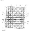
- the pixel blocks 100R, 100Gr, 100Gb, and 100B are arranged in two rows ⁇ two columns, for example. Specifically, the pixel block 100R and the pixel block 100B having the same arrangement pattern and the pixel block 100Gr and the pixel block 100Gb having the same arrangement pattern are arranged respectively on diagonal lines intersecting each other. As an example, the pixel block 100Gr is disposed on the upper left, the pixel block 100R is disposed on the upper right, the pixel block 100B is disposed on the lower left, and the pixel block 100Gb is disposed on the lower right. In such a manner, the pixel blocks 100R, 100Gr, 100Gb, and 100B are arranged in a so-called Bayer arrangement in units of pixel blocks 100.
- the plurality of lenses 101 is each a so-called on-chip lens, and is provided on the color filters 131 on the light incident side S of the pixel array 11.
- the lens 101 is provided over the two light-receiving pixels P (pixel pair 90A) adjacent to each other in the X-axis direction.
- Four lenses 101 are provided over the eight light-receiving pixels P in the pixel block 100R.
- Five lenses 101 are provided over the ten light-receiving pixels P in the pixel block 100Gr.
- Five lenses 101 are provided over the ten light-receiving pixels P in the pixel block 100Gb.
- Four lenses 101 are provided over the eight light-receiving pixels P in the pixel block 100B.
- the lenses 101 are provided side by side in the X-axis direction and a Y-axis direction.
- the lenses 101 side by side in the Y-axis direction are arranged to be shifted from each other in the X-axis direction by one light-receiving pixel P.
- the pixel pairs 90A side by side in the Y-axis direction are arranged to be shifted from each other in the X-axis direction by one light-receiving pixel P.
- the pixel array 11 includes a plurality of control lines TRGL, a plurality of control lines RSTL, a plurality of control lines SELL, and a plurality of signal lines VSL.
- the control line TRGL corresponds to a specific example of a "control line" in the present disclosure.
- the control lines TRGL extend in the X-axis direction (see, e.g., FIGs. 16 to 18 ), and have respective one ends coupled to the drive section 12.
- the drive section 12 supplies control signals STRG to the control lines TRGL.
- the control lines RSTL extend in the X-axis direction (see, e.g., FIG. 16 ), and have respective one ends coupled to the drive section 12.
- the drive section 12 supplies control signals SRST to the control lines RSTL.
- the control lines SELL extend in the X-axis direction (see, e.g., FIG. 16 ), and have respective one ends coupled to the drive section 12.
- the drive section 12 supplies control signals SSEL to the control lines SELL.
- the signal lines VSL extend in the Y-axis direction (see, e.g., FIG. 19 ), and have respective one ends coupled to the readout section 20.
- the signal lines VSL transfer the signals SIG generated by the light-receiving pixels P to the readout section 20.
- the pixel block 100Gr ( FIG. 4 ) includes, for example, ten photodiodes, ten transistors TRG, five floating diffusion layers (FD), and one transistor RST, one transistor AMP and one transistor SEL, each as a pixel transistor.
- the ten photodiodes and the ten transistors TRG each respectively correspond to the ten light-receiving pixels PGr included in the pixel block 100Gr.
- the five floating diffusion layers are arranged one by one for the respective pixel pairs 90A. In other words, each of the five floating diffusion layers is shared by the two light-receiving pixels P constituting the pixel pair 90A and being adjacent to each other in the X-axis direction.
- the transistors TRG, RST, AMP, and SEL in this example are each an N-type MOS (Metal Oxide Semiconductor) transistor.
- the five floating diffusion layers and the transistors TRG, RST, AMP, and SEL are each provided on the front surface 111S1 of the semiconductor substrate 111.
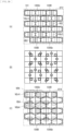
- FIG. 6 illustrates an example of a planar configuration in each of the plurality of light-receiving pixels P constituting the pixel blocks 100R, 100Gr, 100Gb, and 100B.
- the five or four floating diffusion layers provided in each of the pixel blocks 100R, 100Gr, 100Gb, and 100B are shared by the two light-receiving pixels P constituting the pixel pair 90A and being adjacent to each other in the X-axis direction.
- the floating diffusion layer is disposed at a boundary between the two light-receiving pixels P constituting the pixel pair 90A and being adjacent to each other in the X-axis direction.
- one floating diffusion layer and the gates of the two transistors TRG arranged to be opposed to each other provided for each of the pixel pairs 90A are each arranged to be one-sided toward one (e.g., a lower side on the sheet) of a pair of sides opposed to each other in the Y-axis direction in each of the pixel pairs 90A.
- the positions of the one floating diffusion layer and the gates of the two transistors TRG arranged to be opposed to each other provided for each of the pixel pairs 90A are not limited thereto.
- the one floating diffusion layer and the gates of the two transistors TRG arranged to be opposed to each other provided for each of the pixel pairs 90A may be arranged to be one-sided toward one (e.g., a lower side on the sheet), of a pair of sides opposed to each other in the Y-axis direction, and toward the other (e.g., a lower side on the sheet) thereof, on every other row.
- the plurality of light-receiving pixels P constituting the pixel blocks 100R, 100Gr, 100Gb, and 100B are arranged cyclically in the Y-axis direction by using, as a pixel pair 90B, two light-receiving pixels P adjacent to each other in the Y-axis direction. Further, two light-receiving pixels P adjacent to each other in the X-axis direction of the pixel pairs 90B mutually have a mirror image structure, as illustrated in FIG. 6 , for example.
- FIG. 8 illustrates an example of a planar arrangement of pixel transistors provided for each of the pixel blocks 100R, 100Gr, 100Gb, and 100B.
- the pixel transistor includes the transistors RST, AMP, and SEL, and one transistor RST, one transistor AMP and one transistor SEL are provided for each of the pixel blocks 100R, 100Gr, 100Gb, and 100B.
- a unit U including the pixel blocks 100R, 100Gr, 100Gb, and 100B includes 12 pixel transistors (RST-R, RST-Gr, RST-Gb, RST-B, AMP-R, AMP-Gr, AMP-Gb, AMP-B, SEL-R, SEL-Gr, SEL-Gb, and SEL-B).
- R, Gr, Gb, and B attached to the end of each symbol of the pixel transistors correspond to the pixel blocks 100R, 100Gr, 100Gb, and 100B in which the respective pixel transistors are provided.
- R, Gr, Gb, and B attached to the end thereof are omitted.
- the 12 pixel transistors are provided to be divided into three groups of four pixel transistors (e.g., [RST-Gr, RST-B/RST-R/RST-Gb]/ [AMP-Gr/SEL-Gr/SEL-R/AMP-R]/ [AMP-B/SEL-B/SEL-Gb/AMP-Gb]), for example.
- the four pixel transistors of each group are provided side by side, for example, along the X-axis direction. For example, as illustrated in FIG.
- the one floating diffusion layer and the gates of the two transistors TRG arranged to be opposed to each other provided for each of the pixel pairs 90A are arranged to be one-sided toward one (e.g., a lower side on the sheet), of a pair of sides opposed to each other in the Y-axis direction, and toward the other side (e.g., a lower side on the sheet) thereof, on every other row, four pixel transistors of each group are provided side by side at the boundary between two light-receiving pixels P adjacent to each other in the Y-axis direction, as illustrated in FIG. 8 , for example.
- the four pixel transistors of each group at the boundary between two light-receiving pixels P adjacent to each other in the Y-axis direction are shared by the two light-receiving pixels P adjacent to each other in the Y-axis direction. This improves area efficiency.
- the four pixel transistors of each group are arranged cyclically in each of the X-axis direction and the Y-axis direction. A cycle in the X-axis direction is larger than a cycle in the Y-axis direction, and is twice larger, for example.
- Element separation sections 115 and 116 are provided, in a plan view, above and below the plurality of pixel transistors provided side by side along the X-axis direction and between the plurality of pixel transistors provided side by side, respectively.
- the element separation section 115 electrically separates a diffusion region 114 and the light-receiving section 112 from each other.
- the diffusion region 114 in which N-type impurities are diffused, is provided on the front surface 111S1 of the semiconductor substrate 111 constituting the source/drain of the transistors TRG, RST, AMP, and SEL.
- the element separation section 116 electrically separates the plurality of pixel transistors provided side by side, as appropriate, from each other.
- the element separation sections 115 and 116 are each provided, as an STI (Shallow Trench Isolation) formed using an insulating layer or as an impurity layer, for example, on the front surface 111S1 of the semiconductor substrate 111.
- STI Shallow Trench Isolation
- the floating diffusion layer is formed closer to the element separation section 115 with respect to a line segment passing through the centers of the respective gates of the transistors TRG arranged to be opposed to each other along the X-axis direction, and the floating diffusion layer is brought into contact with the element separation section, for example, as illustrated in FIG. 9 .
- Intentionally avoiding injection of a P-type diffusion layer for securing STI pinning eliminates an electric field of a PN junction generated between the P-type diffusion layer and the floating diffusion layer (N-type diffusion layer), thus suppressing a white spot in the floating diffusion layer.
- the floating diffusion layer is disposed away from the element separation section 115 with respect to the line segment passing through the centers of the respective gates of the transistors TRG arranged to be opposed to each other along the X-axis direction, for example, as illustrated in FIG. 10 .
- This relaxes an electric field generated between the element separation section 115 and the floating diffusion layer, thus suppressing the floating diffusion layer having more white spots.
- a contact floating diffusion layer contact
- a contact floating diffusion layer contact
- the element separation section 115 for separating the photodiode and the pixel transistor from each other is preferably formed using an impurity layer. This enables the dosing amount of P-type ions to be reduced, thus making it possible to further suppress the floating diffusion layer having more white spots, as compared with the case where the element separation section 115 is formed as the STI.
- the element separation section 116 between the pixel transistors of the adjacent light-receiving pixels P is preferably formed by the STI. This enables reduction in a space necessary for the separation, thus making it possible to extend a channel length and a gate width of the pixel transistor.
- a well contact region WellCon for applying fixed electric charge to the semiconductor substrate 111 may be provided between pixel transistors provided side by side for each of the pixel blocks 100R, 100Gr, 100Gb, and 100B. This makes it possible to reduce a surface electric field on the periphery of the light-receiving section 112, as compared with the case of being disposed immediately below the light-receiving section 112 (lower side in FIG. 3 ).
- the well contact region WellCon corresponds to a specific example of a "substrate contact" of the present disclosure.
- the diffusion region 114 may be shared by pixel transistors provided side by side, for example, as illustrated in FIG. 11 . This makes it possible to reduce an area for the formation of pixel transistors.
- a transistor FDG may be further provided in order to switch conversion efficiency.
- the transistors AMP and SEL and the transistors RST and FDG are arranged in different rows in the pixel blocks 100Gr and 100Gb, and the transistors AMP, SEL, RST, and FDG are arranged in the same row in the pixel blocks 100R and 100B.
- This enables the control lines RSTL and FDGL of the transistors RST and FDG to be shared by the pixel block 100R and the pixel block 100Gr provided side by side in the X-axis direction and by the pixel block 100Gb and the pixel block 100B, thus making it possible to reduce the number of control wiring lines.
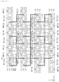
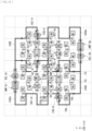
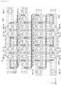
- FIG. 13 illustrates the plurality of floating diffusion layers, the gates of the plurality of transistors TRG, the plurality of pixel transistors (transistors RST, AMP, SEL, and FDG) provided for each of the pixel blocks 100R, 100Gr, 100Gb, and 100B provided on the front surface 111S1 of the semiconductor substrate 111, together with outlines of the pixel blocks 100R, 100Gr, 100Gb, and 100B.
- FIG. 13 illustrates the plurality of floating diffusion layers, the gates of the plurality of transistors TRG, the plurality of pixel transistors (transistors RST, AMP, SEL, and FDG) provided for each of the pixel blocks 100R, 100Gr, 100Gb, and 100B provided on the front surface 111S1 of the semiconductor substrate 111, together with outlines of the pixel blocks 100R, 100Gr, 100Gb, and 100B.
- FIG. 18 illustrates various wiring lines (the plurality of control lines TRGL and FDGL, the plurality of signal lines VSL, the reference potential line VSS, and the power supply line VDDL) provided in the wiring layer 126, for example, together with the outlines of the pixel blocks 100R, 100Gr, 100Gb, and 100B.
- FIG. 19 illustrates various wiring lines (the plurality of signal lines VSL, the reference potential line VSS, and the power supply line VDDL) provided in the wiring layer 127, for example, together with the outlines of the pixel blocks 100R, 100Gr, 100Gb, and 100B.
- the pixel block 100Gr and the pixel block 100Gb having the same arrangement pattern of the light-receiving pixels P and a pixel block R and a pixel block B having the same arrangement pattern of the light-receiving pixels P each have equivalent conversion efficiency. It is therefore possible to simplify a correction circuit in subsequent stage processing. In addition, capacity characteristics are also equivalent, thus making it possible to reduce dispersion of the characteristics.
- the reference signal generation section 13 is configured to generate a reference signal RAMP on the basis of instructions from the imaging control section 18.
- the reference signal RAMP has a so-called ramp waveform in which a voltage level gradually changes with a lapse of time during periods during which the readout section 20 performs AD conversion (the P-phase period TP and the D-phase period TD).
- the reference signal generation section 13 supplies such a reference signal RAMP to the readout section 20.
- FIG. 20 illustrates a configuration example of the readout section 20. It is to be noted that FIG. 20 also illustrates the reference signal generation section 13, the signal processing section 15, and the imaging control section 18 in addition to the readout section 20.
- the readout section 20 includes a plurality of constant current sources 21, a plurality of AD (Analog to Digital) converters ADC, and a transfer controller 27.
- the plurality of constant current sources 21 and the plurality of AD converters ADC are provided in correspondence with the plurality of respective signal lines VSL. In the following, a description is given of the constant current source 21 and the AD converter ADC corresponding to one signal line VSL.
- the AD converter ADC is configured to perform AD conversion on the basis of the signal SIG on the corresponding signal line VSL.
- the AD converter ADC includes capacitors 22 and 23, a comparison circuit 24, a counter 25, and a latch 26.
- the capacitor 22 has one end coupled to the signal line VSL and is to be supplied with the signal SIG, and another end coupled to the comparison circuit 24.
- the capacitor 23 has one end to be supplied with the reference signal RAMP supplied from the reference signal generation section 13, and another end coupled to the comparison circuit 24.
- the imaging device 1 has three imaging modes M (imaging modes MA, MB, and MC).
- the imaging control section 18 selects one of the three imaging modes MA to MC on the basis of the information about the zoom factor included in the control signal Sctl. Specifically, as illustrated in FIG. 22 , the imaging control section 18 selects the imaging mode MA in a case where the zoom factor is less than 2, selects the imaging mode MB in a case where the zoom factor is 2 or more and less than 3, and selects the imaging mode MC in a case where the zoom factor is 3 or more.
- the zoom factor when the zoom factor is increased from one in the imaging mode MA, the number of effective pixels decreases in accordance with the factor. Then, when the zoom factor reaches two, the imaging mode M turns into the imaging mode MB.
- the imaging device 1 generates image data DT1 by calculating a pixel value V corresponding to a received light amount of the left light-receiving pixels P in the pixel pairs 90A provided with the lenses 101 in each of the plurality of pixel blocks 100. Specifically, among the ten light-receiving pixels PGr in the pixel block 100Gr, the imaging device 1 targets the five light-receiving pixels PGr arranged on the left in the five pixel pairs 90A for the readout operation, and thus calculates a pixel value VGr1 at a centroid position of the five light-receiving pixels PGr.
- FIG. 25 illustrates an example of the readout operation, in which (A) illustrates a waveform of the control signal SSEL, (B) illustrates a waveform of the control signal SRST, (C) illustrates a waveform of the control signal STRG (a control signal STRGL) supplied to the light-receiving pixel PGr arranged on the left in the pixel pair 90A, (D) illustrates a waveform of the control signal STRG (a control signal STRGR) supplied to the light-receiving pixel PGr arranged on the right in the pixel pair 90A, (E) illustrates a waveform of the control signal AZ, (F) illustrates a waveform of the reference signal RAMP, (G) illustrates a waveform of the signal SIG, and (H) illustrates a waveform of the signal CP.
- A illustrates a waveform of the control signal SSEL
- B illustrates a waveform of the control signal SRST
- C illustrates a waveform of
- the voltage of the reference signal RAMP falls below the voltage of the signal SIG (the pixel voltage Vpix1) ((F) and (G) of FIG. 25 ).
- the comparison circuit 24 of the AD converter ADC thus changes the voltage of the signal CP from the high level to the low level ((H) of FIG. 25 ).
- the counter 25 of the AD converter ADC stops the counting operation on the basis of the transition of the signal CP.
- the count value (count value CNTD1) of the counter 25 at this time is a value corresponding to the pixel voltage Vpix1.
- the latch 26 holds this count value CNTD1.
- the counter 25 then resets the count value.
- the imaging control section 18 stops generating the clock signal CLK at the end of the D-phase period TD1.
- the reference signal generation section 13 stops changing the voltage of the reference signal RAMP at this timing t20 ((F) of FIG. 25 ).
- the readout section 20 supplies, as the image signal SpicO, the count value CNTD1 held by the latch 26 to the signal processing section 15.
- the drive section 12 changes the respective voltages of the control signals STRGL and STRGR from the low level to the high level ((C) and (D) of FIG. 25 ).
- This brings the transistors TRG into an ON state in the ten light-receiving pixels PGr in the pixel block 100Gr, and causes the electric charge generated at the photodiodes to be transferred to the floating diffusion layer (the electric charge transfer operation).
- the pixel block 100Gr outputs a voltage corresponding to the voltage of the floating diffusion layer at this time. In such a manner, the voltage of the signal SIG becomes a pixel voltage Vpix2 ((G) of FIG. 25 ).
- the imaging mode MA corresponds to a specific example of a "first imaging mode” in the present disclosure.
- the pixel value in the image data DT1 corresponds to a specific example of a "first pixel value” in the present disclosure.
- the pixel value in the image data DT2 corresponds to a specific example of a "second pixel value” in the present disclosure.
- the pixel value in the image data DT3 corresponds to a specific example of a "third pixel value" in the present disclosure.
- the imaging device 1 targets the light-receiving pixel PR arranged on the left in one pixel pair 90A among the four pixel pairs 90A in the pixel block 100R for the readout operation, and calculates the pixel value VR1 at the position of this light-receiving pixel PR. Then, as illustrated in (B) of FIG. 28 , the imaging device 1 next targets the two light-receiving pixels PR in the pixel pair 90A for the readout operation, and calculates the pixel value VR2 at a centroid position of the two light-receiving pixels PR.
- the image data generator 16 performs, for example, the complementing processing on the basis of a plurality of pixel values VB2 in the image data DT2 to thereby calculate pixel values V across a surface, and generates the pixel value VB4 on the basis of the pixel values V across the surface.
- FIG. 19 illustrates an operation example of the imaging device 1 in the imaging mode MC.
- FIG. 20 more specifically illustrates the operation illustrated in FIG. 19 .
- the light-receiving pixels P illustrated with "o" represent the light-receiving pixels P that are targeted for the readout operation.
- FIG. 23 illustrates an example of the remosaic processing in the imaging mode MC, in which (A) illustrates the image data DT1, (B) illustrates the positions of the pixel values V before and after the remosaic processing, and (C) illustrates the image data DT4 generated by the remosaic processing on the basis of the image data DT1.
- " ⁇ " represents the position of the pixel value V in the image data DT1
- "o" represents the position of the pixel value V in the image data DT4.
- the image data generator 16 performs, for example, complementing processing on the basis of a plurality of pixel values VR1 in the image data DT1 to thereby calculate pixel values V across a surface, and generates the pixel value VR4 on the basis of the pixel values V across the surface.
- the image data generator 16 performs, for example, the complementing processing on the basis of a plurality of pixel values VGr1 and VGb1 in the image data DT1 to thereby calculate pixel values V across a surface, and generates the pixel values VGr4 and VGb4 on the basis of the pixel values V across the surface.
- FIG. 24A the image data generator 16 performs, for example, complementing processing on the basis of a plurality of pixel values VR1 in the image data DT1 to thereby calculate pixel values V across a surface, and generates the pixel values VGr4 and VGb4 on the basis of the pixel values V across the surface.
- the imaging device 1 is provided with the plurality of pixel blocks 100 that each includes the plurality of light-receiving pixels P including the color filters of mutually the same color.
- the plurality of light-receiving pixels P is divided into the plurality of pixel pairs 90A each including two light-receiving pixels P.
- the plurality of lenses 101 is provided at the respective positions corresponding to the plurality of pixel pairs 90A.
- the floating diffusion layer disposed at the boundary between the two light-receiving pixels P constituting the pixel pair 90A and being adjacent to each other in the X-axis direction is disposed to be shifted in the Y-axis direction with respect to the line segment passing through the centers of the gates of the two transistors TRG opposed to each other along the X-axis direction.
- the floating diffusion layer is set close to the element separation section 115.
- the floating diffusion layer is disposed away from the element separation section 115. This makes it possible to suppress the floating diffusion layer having more white spots.
- some of the plurality of control lines TRGL are provided to be along the coupling wiring line FDL that couples the four or five floating diffusion layers and the gates of the transistors AMP together in each of the pixel blocks 100R, 100Gr, 100Gb, and 100B.
- This improves the coupling between the coupling wiring line FDL and the control line TRGL and suppresses the coupling between the coupling wiring line FDL and the plurality of other control lines RSTL, SELL, and FDGL as well as the plurality of signal lines VSL. It is therefore possible to improve a transfer auxiliary effect by the control line TRGL.
- a gate length of the transistor AMP is extended, for example, it is possible to reduce a random telegraph noise (RTS).
- RTS random telegraph noise
- a gate length of the transistors SEL and RST it is possible to reduce dispersion of the characteristics of the transistor such as a threshold voltage (Vth) and cut-off.
- the foregoing embodiment exemplifies the case where the four pixel blocks 100R, 100Gr, 100Gb, and 100B arranged in two rows ⁇ two columns are used as the minimum repeating unit (unit U); however, this is not limitative.
- the total of eight pixel blocks including two pixel blocks 100R, 100Gr, 100Gb, and 100B may be used as the minimum repeating unit. In such a case, the total of eight pixel blocks are arranged, for example, in four rows ⁇ two columns.
- VDDs are provided between the pixel transistors, as in [FD/ FDG/ RST/ VDD/ AMP/ SEL/ VSL]/ [FD/ FDG/ VDD/ RST/ FDG/ FD]/ [VSL/ SEL/ AMP/ VDD/ RST/ FDG/ FD].
- the third substrate 230 includes, in a semiconductor substrate 231, a logic circuit 52 that processes a pixel signal.
- a logic circuit 32 includes, for example, a vertical drive circuit 53, a column signal processing circuit 54, a horizontal drive circuit 55, and a system control circuit 56.
- the logic circuit 52 (specifically, the horizontal drive circuit 55) outputs an output voltage Vout for each of the light-receiving pixels P to the outside.
- a low-resistance region including silicide, formed using salicide (Self Aligned Silicide) process, such as CoSi 2 or NiSi may be formed on a surface of an impurity diffusion region in contact with a source electrode and a drain electrode.
- the p-well 242 is configured by a p-type semiconductor region.
- the PD 241 is configured by a semiconductor region of an electrically-conductive type (specifically, n-type) different from that of the p-well 242.
- the semiconductor substrate 211 includes, in the p-well 242, a floating diffusion layer (FD) as the semiconductor region of an electrically-conductive type (specifically, n-type) different from that of the p-well 242.
- FD floating diffusion layer
- the second substrate 220 is configured by stacking an insulating layer 252 on the semiconductor substrate 221.
- the second substrate 220 includes the insulating layer 252 as a portion of the interlayer insulating film 251.
- the insulating layer 252 is provided between the semiconductor substrate 221 and the semiconductor substrate 231.
- the semiconductor substrate 221 is configured by a silicon substrate.
- the second substrate 220 includes one readout circuit 222 for every four light-receiving pixels P.
- the second substrate 220 has a configuration in which the readout circuit 222 is provided on a portion of the semiconductor substrate 221 on a side of a front surface (a surface 221S1 opposed to the third substrate 230).
- a stack including the first substrate 210 and the second substrate 220 includes the interlayer insulating film 251 and the through-wiring line 254 provided in the interlayer insulating film 251.
- the above-described stack includes one through-wiring line 254 for each of the light-receiving pixels P.
- the through-wiring line 254 extends in a normal direction of the semiconductor substrate 221, and is provided to penetrate a location, of the interlayer insulating film 251, including the insulating layer 253.
- the first substrate 210 and the second substrate 220 are electrically coupled to each other by the through-wiring line 254.
- the through-wiring line 254 is electrically coupled to the floating diffusion layer and a coupling wiring line 255 described later.
- the stack including the first substrate 210 and the second substrate 220 further includes a through-wiring line (unillustrated) provided in the interlayer insulating film 251 and electrically coupled, for example, to the p-well 242 of the semiconductor substrate 211, a wiring line in the second substrate 220, and a transfer gate TG and a pixel drive line 43.
- the transfer gate TG has a vertical gate structure, and is formed deeper than a depth of the element separation section 115.
- the transfer gate TG is disposed at a position deviated from the center of the light-receiving pixel P in a plan view.
- the second substrate 220 includes, in the insulating layer 252, for example, a plurality of coupling sections 259 electrically coupled to the readout circuit 42 and the semiconductor substrate 221.
- the second substrate 220 further includes, for example, a wiring layer 256 on the insulating layer 252.
- the wiring layer 256 includes, for example, an insulating layer 257, a plurality of pixel drive lines 43 provided in the insulating layer 257, and a plurality of vertical signal lines 424.
- the wiring layer 256 further includes, in the insulating layer 257, for example, a plurality of coupling wiring lines 255, with one coupling wiring lines 255 being provided for every four light-receiving pixels P.
- the coupling wiring line 255 electrically couples together the through-wiring lines 254 electrically coupled to the respective floating diffusion layers included in the four light-receiving pixels P sharing the readout circuit 42.
- the wiring layer 262 includes, for example, an insulating layer 263 and a plurality of pad electrodes 264 provided in the insulating layer 263.
- the plurality of pad electrodes 264 is electrically coupled to the logic circuit 52.
- Each of the pad electrodes 264 is configured by Cu (copper), for example.
- Each of the pad electrodes 264 is exposed to a front surface of the wiring layer 262.
- Each of the pad electrodes 264 is used to electrically couple the second substrate 220 and the third substrate 230 to each other and to attach the second substrate 220 and the third substrate 230 to each other.
- the plurality of pad electrodes 264 may not necessarily be provided, and only one pad electrode 264 can be enough to be electrically coupled to the logic circuit 52.
- the second substrate 220 and the third substrate 230 are electrically coupled to each other by a junction between the pad electrodes 258 and 264. That is, the gate (transfer gate TG) of the transfer transistor TR is electrically coupled to the logic circuit 52 via the through-wiring line 254 and the pad electrodes 258 and 264.
- the third substrate 230 is attached to the second substrate 220, with the front surface (surface 231S1) of the semiconductor substrate 231 being opposed to the side of the front surface (surface 221S1) of the semiconductor substrate 221. That is, the third substrate 230 is attached face-to-face to the second substrate 220.
- the photodiode and the pixel transistor are provided in different substrates.
- the gate length of the transistor AMP is extended, for example, it is possible to reduce the random telegraph noise (RTS).
- RTS random telegraph noise
- the gate lengths of the transistors SEL and RST it is possible to reduce the dispersion of the transistor characteristics such as the threshold voltage (Vth) and the cut-off.
- FIG. 37A illustrates an example of a configuration of the pixel block 100Gr upon the addition of the transistor FDG.
- FIG. 37B illustrates another example of the configuration of the pixel block 100Gr upon the addition of the transistor FDG.
- FIG. 37C illustrating an example of a configuration of the pixel block 100R upon the addition of the transistor FDG.
- FIG. 37D illustrates another example of the configuration of the pixel block 100R upon the addition of the transistor FDG.
- the plurality of SubFDs may be arranged, with one SubFD being provided for one transistor FDG, or may be shared by a plurality of transistors FDG.
- the adjacent coupling wiring line FDL may serve as the plurality of SubFDs.
- FIG. 38 illustrates various wiring lines (the coupling wiring lines SubFDL of the plurality of SubFDs, the plurality of control lines SELL, the plurality of signal lines VSL, the reference potential line VSS, and the power supply line VDDL) according to Modification Example 5 of the present disclosure provided in the wiring layer 123, for example, together with the outlines of the pixel blocks 100R, 100Gr, 100Gb, and 100B.
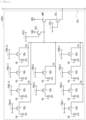
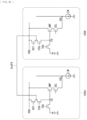
- FIG. 39 is a circuit diagram illustrating configurations of the pixel blocks illustrated in FIG. 38 . It is to be noted that FIG. 39 illustrates the plurality of light-receiving pixels P constituting each of the pixel blocks (pixel blocks 100Gb and 100R) with one PD in a simplified manner.
- the pixel blocks 100R and 100B each including eight light-receiving pixels P and the pixel blocks 100Gr and 100Gb each including ten light-receiving pixels P may share the FD with each other via the SubFD.
- the SubFD is a metal wiring line coupled to a node between the transistor FDG and the transistor RST and provided to secure a capacity upon driving at low conversion efficiency.
- the SubFD corresponds to a specific example of a "conversion efficiency switching wiring line" in the present disclosure.
- a conversion efficiency switching wiring line (SubFD) of the pixel block 100Gb and the SubFD of the pixel block 100R, which are adjacent to each other in the Y-axis direction, are coupled to each other via the coupling wiring line SubFDL.
- one end of the coupled SubFD is coupled to a source of the transistor RST and a drain of the transistor FDG of the pixel block 100Gb, and the other end thereof is coupled to a source of the transistor RST and a drain of the transistor FDG of the pixel block 100R.
- the SubFD of the pixel block 100B and the SubFD of the pixel block 100Gr which are adjacent to each other in the Y-axis direction, are electrically coupled to each other via the coupling wiring line SubFDL.
- one end of the coupled SubFD is coupled to a source of the transistor RST and a drain of the transistor FDG of the pixel block 100B, and the other end thereof is coupled to a source of the transistor RST and a drain of the transistor FDG of the pixel block 100Gr.
- FIG. 38 illustrates the coupling wiring line SubFDL having a narrower linewidth than a linewidth of the SubFD for the sake of convenience, this is not limitative. In actuality, the coupling wiring line SubFDL is formed to have a linewidth equivalent to the linewidth of the SubFD.
- the pixel blocks e.g., the pixel block 100Gb and the pixel block 100R or the pixel block 100B and the pixel block 100Gr
- the pixel blocks e.g., the pixel block 100Gb and the pixel block 100R or the pixel block 100B and the pixel block 100Gr
- the pixel blocks adjacent to each other in the Y-axis direction to each efficiently utilize the capacity of the SubFD provided in each of the pixel blocks, thus making it possible to expand a dynamic range. Additionally, it is possible to further lower the conversion efficiency during low conversion efficiency (Low).
- the FD is shared, via the SubFD, between the pixel block 100R including eight light-receiving pixels P and the pixel block 100Gb including ten light-receiving pixels P, which are adjacent to each other in the Y-axis direction, and between the pixel block 100B including eight light-receiving pixels P and the pixel block 100Gr including ten light-receiving pixels P, which are adjacent to each other in the Y-axis direction.
- the number of constituent pixels sharing the FD in the unit U is 18 in both cases, thus reducing the difference in the conversion efficiency during the low conversion efficiency (Low). It is therefore possible to commonalize the two analog circuits provided for the Low system in order to address the difference in the conversion efficiency in the foregoing embodiment or the like.
- the SubFD shared between the pixel blocks adjacent to each other in the Y-axis direction is coupled to the sources of the transistors RST of the respective pixel blocks.
- bringing at least one of the transistors RST of the pixel blocks sharing the FD into an ON state and bringing the transistor FDG into an OFF state during high conversion efficiency (High) allow the SubFD to be fixed to a power supply potential (VDD).
- VDD power supply potential
- FIG. 40 illustrates various wiring lines (the coupling wiring lines SubFDL of the plurality of SubFDs, the plurality of control lines SELL, the plurality of signal lines VSL, the reference potential line VSS, and the power supply line VDDL) according to Modification Example 6 of the present disclosure provided in the wiring layer 123, for example, together with the outlines of the pixel blocks 100R, 100Gr, 100Gb, and 100B.
- FIG. 41 is a circuit diagram illustrating configurations of pixel blocks illustrated in FIG. 40 . It is to be noted that FIG. 41 illustrates the plurality of light-receiving pixels P constituting each of the pixel blocks (pixel blocks 100Gb and 100R) with one PD in a simplified manner.
- a switch element 117 may be disposed in the middle of the SubFD coupled to the source of the transistor RST and the drain of the transistor FDG of the pixel block 100Gb and the source of the transistor RST and the drain of the transistor FDG of the pixel block 100R, which are adjacent to each other in the Y-axis direction.
- the switch element 117 may be disposed in the middle of the SubFD coupled to the source of the transistor RST and the drain of the transistor FDG of the pixel block 100B and the source of the transistor RST and the drain of the transistor FDG of the pixel block 100Gr, which are adjacent to each other in the Y-axis direction.
- a portion of the SubFD is switched to another wiring layer (e.g., the wiring layer 122) near the switch element 117 using a via to control coupling and decoupling of the SubFD by switching ON/OFF the switch element 117.
- the switch element 117 is brought into an OFF state during the high conversion efficiency (High), and the switch element 117 is brought into an ON state during the low conversion efficiency (Low).
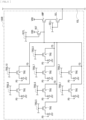
- FIG. 42 is a circuit diagram illustrating configurations of pixel blocks according to Modification Example 7 of the present disclosure. It is to be noted that FIG. 42 illustrates the plurality of light-receiving pixels P constituting each of the pixel blocks (pixel blocks 100Gb and 100R) with one PD in a simplified manner.
- FIG. 43 is a timing chart diagram of each of the transistors in the pixel blocks illustrated in FIG. 42 upon driving at the high conversion efficiency and upon driving at the low conversion efficiency.
- the foregoing Modification Example 5 exemplifies the SubFD being fixed to the power supply potential (VDD) during the high conversion efficiency (High), but this is not limitative.
- the drain of the transistor RST may be coupled to another power supply line (VB), and a changeover switch disposed outside the pixel array may be used for coupling to the power supply potential (VDD) when the pixel is reset and for coupling to a fixed potential (e.g., GND) during an accumulation period and the high conversion efficiency (High).
- a fixed potential e.g., GND
- FIG. 44 is a circuit diagram illustrating configurations of pixel blocks according to Modification Example 8 of the present disclosure. It is to be noted that FIG. 44 illustrates the plurality of light-receiving pixels P constituting each of the pixel blocks (pixel blocks 100Gb and 100R) with one PD in a simplified manner.
- the foregoing Modification Examples 5 to 7 exemplify the transistor RST and the transistor FDG being coupled in series in the pixel blocks 100R, 100Gr, 100Gb, and 100B, but this is not limitative.
- the transistor RST and the transistor FDG may be coupled in parallel with respect to the FD as illustrated in FIG. 44 .
- the foregoing Modification Examples 5 to 8 exemplify the sharing of the SubFD by the pixel block 100Gb and the pixel block 100R adjacent to each other in the Y-axis direction and the sharing of the SubFD by the pixel block 100B and the pixel block 100Gr adjacent to each other in the Y-axis direction, but this is not limitative.
- the SubFD may be shared by the pixel block 100Gr and the pixel block 100R adjacent to each other in the X-axis direction and may be shared by the pixel block 100Gb and pixel block 100B adjacent to each other in the X-axis direction.
- FIG. 47 illustrates a usage example of the imaging device 1 according to the foregoing embodiment.
- the imaging device 1 described above is usable in a variety of cases of sensing light, including visible light, infrared light, ultraviolet light, and X-rays as follows.
- the technology (the present technology) according to the present disclosure is applicable to a variety of products.
- the technology according to the present disclosure may be achieved as an apparatus to be installed aboard any type of mobile body such as an automobile, an electric vehicle, a hybrid electric vehicle, a motorcycle, a bicycle, a personal mobility, an airplane, a drone, a vessel, or a robot.
- FIG. 48 is a block diagram depicting an example of schematic configuration of a vehicle control system as an example of a mobile body control system to which the technology according to an embodiment of the present disclosure can be applied.
- the vehicle control system 12000 includes a plurality of electronic control units connected to each other via a communication network 12001.
- the vehicle control system 12000 includes a driving system control unit 12010, a body system control unit 12020, an outside-vehicle information detecting unit 12030, an in-vehicle information detecting unit 12040, and an integrated control unit 12050.
- a microcomputer 12051, a sound/image output section 12052, and a vehicle-mounted network interface (I/F) 12053 are illustrated as a functional configuration of the integrated control unit 12050.
- the driving system control unit 12010 controls the operation of devices related to the driving system of the vehicle in accordance with various kinds of programs.
- the driving system control unit 12010 functions as a control device for a driving force generating device for generating the driving force of the vehicle, such as an internal combustion engine, a driving motor, or the like, a driving force transmitting mechanism for transmitting the driving force to wheels, a steering mechanism for adjusting the steering angle of the vehicle, a braking device for generating the braking force of the vehicle, and the like.
- the body system control unit 12020 controls the operation of various kinds of devices provided to a vehicle body in accordance with various kinds of programs.
- the body system control unit 12020 functions as a control device for a keyless entry system, a smart key system, a power window device, or various kinds of lamps such as a headlamp, a backup lamp, a brake lamp, a turn signal, a fog lamp, or the like.
- radio waves transmitted from a mobile device as an alternative to a key or signals of various kinds of switches can be input to the body system control unit 12020.
- the body system control unit 12020 receives these input radio waves or signals, and controls a door lock device, the power window device, the lamps, or the like of the vehicle.
- the outside-vehicle information detecting unit 12030 detects information about the outside of the vehicle including the vehicle control system 12000.
- the outside-vehicle information detecting unit 12030 is connected with an imaging section 12031.
- the outside-vehicle information detecting unit 12030 makes the imaging section 12031 image an image of the outside of the vehicle, and receives the imaged image.
- the outside-vehicle information detecting unit 12030 may perform processing of detecting an object such as a human, a vehicle, an obstacle, a sign, a character on a road surface, or the like, or processing of detecting a distance thereto.
- the imaging section 12031 is an optical sensor that receives light, and which outputs an electric signal corresponding to a received light amount of the light.
- the imaging section 12031 can output the electric signal as an image, or can output the electric signal as information about a measured distance.
- the light received by the imaging section 12031 may be visible light, or may be invisible light such as infrared rays or the like.
- the in-vehicle information detecting unit 12040 detects information about the inside of the vehicle.
- the in-vehicle information detecting unit 12040 is, for example, connected with a driver state detecting section 12041 that detects the state of a driver.
- the driver state detecting section 12041 for example, includes a camera that images the driver.
- the in-vehicle information detecting unit 12040 may calculate a degree of fatigue of the driver or a degree of concentration of the driver, or may determine whether the driver is dozing.
- the microcomputer 12051 can calculate a control target value for the driving force generating device, the steering mechanism, or the braking device on the basis of the information about the inside or outside of the vehicle which information is obtained by the outside-vehicle information detecting unit 12030 or the in-vehicle information detecting unit 12040, and output a control command to the driving system control unit 12010.
- the microcomputer 12051 can perform cooperative control intended to implement functions of an advanced driver assistance system (ADAS) which functions include collision avoidance or shock mitigation for the vehicle, following driving based on a following distance, vehicle speed maintaining driving, a warning of collision of the vehicle, a warning of deviation of the vehicle from a lane, or the like.
- ADAS advanced driver assistance system
- the microcomputer 12051 can perform cooperative control intended for automated driving, which makes the vehicle to travel automatedly without depending on the operation of the driver, or the like, by controlling the driving force generating device, the steering mechanism, the braking device, or the like on the basis of the information about the outside or inside of the vehicle which information is obtained by the outside-vehicle information detecting unit 12030 or the in-vehicle information detecting unit 12040.
- the microcomputer 12051 can output a control command to the body system control unit 12020 on the basis of the information about the outside of the vehicle which information is obtained by the outside-vehicle information detecting unit 12030.
- the microcomputer 12051 can perform cooperative control intended to prevent a glare by controlling the headlamp so as to change from a high beam to a low beam, for example, in accordance with the position of a preceding vehicle or an oncoming vehicle detected by the outside-vehicle information detecting unit 12030.
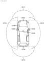
- FIG. 49 is a diagram depicting an example of the installation position of the imaging section 12031.
- the imaging section 12031 includes imaging sections 12101, 12102, 12103, 12104, and 12105.
Landscapes
- Engineering & Computer Science (AREA)
- Multimedia (AREA)
- Signal Processing (AREA)
- Physics & Mathematics (AREA)
- Spectroscopy & Molecular Physics (AREA)
- Solid State Image Pick-Up Elements (AREA)
- Color Television Image Signal Generators (AREA)
- Transforming Light Signals Into Electric Signals (AREA)
Abstract
Description
- The present disclosure relates to an imaging device that captures an image of a subject.
- Some imaging devices obtain an image-plane phase difference in order to achieve auto-focus, for example. For example,
PTL 1 discloses an imaging device including a normal pixel and a phase difference detection pixel to obtain the image-plane phase difference. - PTL 1: International Publication No.
WO2016/098640 - An imaging device is desired to have high image quality of a captured image, and a further improvement in image quality is expected.
- It is desirable to provide an imaging device that makes it possible to enhance image quality.
- An imaging device according to an embodiment of the present disclosure includes: a plurality of pixel blocks each including a plurality of light-receiving pixels including color filters of same color, the plurality of light-receiving pixels being divided into a plurality of first pixel pairs each including two light-receiving pixels adjacent to each other in a first direction; a plurality of lenses provided at respective positions corresponding to the plurality of first pixel pairs; and a plurality of floating diffusion layers each disposed at a boundary between the two light-receiving pixels, of the plurality of first pixel pairs, adjacent to each other in the first direction, the plurality of floating diffusion layers each shared in the plurality of first pixel pairs.
- The imaging device according to the embodiment of the present disclosure is provided with the plurality of light-receiving pixels including the color filters of the same color in each of the plurality of pixel blocks. The plurality of light-receiving pixels is divided into the plurality of first pixel pairs each including two light-receiving pixels adjacent to each other in the first direction. The plurality of lenses is provided at respective positions corresponding to the plurality of first pixel pairs. Further, the plurality of respective first pixel pairs shares the plurality of floating diffusion layers each provided at a boundary between the two light-receiving pixels adjacent to each other in the first direction. This reduces the capacity of the floating diffusion layer and reduces a random noise by increasing efficiency of converting signal charge into a signal voltage.
-
- [
FIG. 1] FIG. 1 is a block diagram illustrating a configuration example of an imaging device according to an embodiment of the present disclosure. - [
FIG. 2] FIG. 2 is an explanatory diagram illustrating a configuration example of a pixel array illustrated inFIG. 1 . - [
FIG. 3] FIG. 3 is a schematic view of an example of a cross-sectional configuration of light-receiving pixels illustrated inFIG. 2 . - [
FIG. 4] FIG. 4 is a circuit diagram illustrating a configuration example of a pixel block illustrated inFIG. 2 . - [
FIG. 5] FIG. 5 is a circuit diagram illustrating a configuration example of another pixel block illustrated inFIG. 2 . - [
FIG. 6] FIG. 6 is an explanatory diagram illustrating an example of a planar arrangement of the light-receiving pixels illustrated inFIG. 2 . - [
FIG. 7] FIG. 7 is a schematic view of another example of the planar arrangement of the light-receiving pixels illustrated inFIG. 2 . - [
FIG. 8] FIG. 8 is an explanatory diagram illustrating an example of a planar arrangement of pixel transistors in the pixel blocks illustrated inFIG. 2 . - [
FIG. 9] FIG. 9 is an explanatory diagram illustrating an example of a planar disposition of a floating diffusion layer in the light-receiving pixel illustrated inFIG. 2 . - [
FIG. 10] FIG. 10 is an explanatory diagram illustrating another example of the planar disposition of the floating diffusion layer in the light-receiving pixel illustrated inFIG. 2 . - [
FIG. 11] FIG. 11 is an explanatory diagram illustrating another example of the planar arrangement of the pixel transistors in the pixel blocks illustrated inFIG. 2 . - [
FIG. 12] FIG. 12 is an explanatory diagram illustrating another example of the planar arrangement of the pixel transistors in the pixel blocks illustrated inFIG. 2 . - [
FIG. 13] FIG. 13 is an explanatory plan view of an example of a wiring layout in the pixel blocks illustrated inFIG. 2 . - [
FIG. 14] FIG. 14 is an explanatory plan view of an example of the wiring layout in the pixel blocks illustrated inFIG. 2 . - [
FIG. 15] FIG. 15 is an explanatory plan view of an example of the wiring layout in the pixel blocks illustrated inFIG. 2 . - [
FIG. 16] FIG. 16 is an explanatory plan view of an example of the wiring layout in the pixel blocks illustrated inFIG. 2 . - [
FIG. 17] FIG. 17 is an explanatory plan view of an example of the wiring layout in the pixel blocks illustrated inFIG. 2 . - [
FIG. 18] FIG. 18 is an explanatory plan view of an example of the wiring layout in the pixel blocks illustrated inFIG. 2 . - [
FIG. 19] FIG. 19 is an explanatory plan view of an example of the wiring layout in the pixel blocks illustrated inFIG. 2 . - [
FIG. 20] FIG. 20 is a block diagram illustrating a configuration example of a readout section illustrated inFIG. 1 . - [
FIG. 21] FIG. 21 is an explanatory diagram illustrating a configuration example of an image signal illustrated inFIG. 1 . - [
FIG. 22] FIG. 22 is an explanatory diagram illustrating an example of the number of effective pixels in the imaging device illustrated inFIG. 1 . - [
FIG. 23] FIG. 23 is an explanatory diagram illustrating an operation example of a plurality of imaging modes in the imaging device illustrated inFIG. 1 . - [
FIG. 24] FIG. 24 is an explanatory diagram illustrating an operation example of the imaging device illustrated inFIG. 1 . - [
FIG. 25] FIG. 25 is a timing waveform chart illustrating an example of a readout operation in the imaging device illustrated inFIG. 1 . - [
FIG. 26] FIG. 26 is another explanatory diagram illustrating an operation example of the imaging device illustrated inFIG. 1 . - [
FIG. 27] FIG. 27 is another explanatory diagram illustrating an operation example of the imaging device illustrated inFIG. 1 . - [
FIG. 28] FIG. 28 is another explanatory diagram illustrating an operation example of the imaging device illustrated inFIG. 1 . - [
FIG. 29] FIG. 29 is another explanatory diagram illustrating an operation example of the imaging device illustrated inFIG. 1 . - [
FIG. 30] FIG. 30 is an explanatory diagram illustrating an example of remosaic processing in the imaging device illustrated inFIG. 1 . - [
FIG. 31A] FIG. 31A is an explanatory diagram illustrating an example of the remosaic processing illustrated inFIG. 30 . - [
FIG. 31B] FIG. 31B is another explanatory diagram illustrating the example of the remosaic processing illustrated inFIG. 30 . - [
FIG. 31C] FIG. 31C is another explanatory diagram illustrating the example of the remosaic processing illustrated inFIG. 30 . - [
FIG. 32] FIG. 32 is an explanatory diagram illustrating an example of a planar arrangement of pixel transistors in pixel blocks constituting an imaging device according to Modification Example 1 of the present disclosure. - [
FIG. 33] FIG. 33 is an explanatory diagram illustrating another configuration example of pixel blocks constituting an imaging device according to Modification Example 2 of the present disclosure. - [
FIG. 34] FIG. 34 is a diagram illustrating an example of an arrangement of pixel transistors and power supply voltages in an imaging device (A) of the embodiment or the like and an imaging device (B) illustrated inFIG. 33 . - [
FIG. 35] FIG. 35 is a schematic view of an example of a cross-sectional configuration of an imaging device according to Modification Example 3 of the present disclosure in a vertical direction. - [
FIG. 36] FIG. 36 is a diagram illustrating an example of an outline configuration of the imaging device illustrated inFIG. 35 . - [
FIG. 37A] FIG. 37A is a circuit diagram illustrating an example of a configuration of a pixel block upon addition of a transistor FDG as the pixel transistor. - [
FIG. 37B] FIG. 37B is a circuit diagram illustrating another example of the configuration of the pixel block upon the addition of the transistor FDG as the pixel transistor. - [
FIG. 37C] FIG. 37C is a circuit diagram illustrating an example of a configuration of another pixel block upon the addition of the transistor FDG as the pixel transistor. - [
FIG. 37D] FIG. 37D is a circuit diagram illustrating another example of the configuration of the other pixel block upon the addition of the transistor FDG as the pixel transistor. - [
FIG. 38] FIG. 38 is an explanatory plan view of an example of a wiring layout in pixel blocks according to Modification Example 5 of the present disclosure. - [
FIG. 39] FIG. 39 is a circuit diagram illustrating configurations of the pixel blocks illustrated inFIG. 38 . - [
FIG. 40] FIG. 40 is an explanatory plan view of an example of a wiring layout in pixel blocks according to Modification Example 6 of the present disclosure. - [
FIG. 41] FIG. 41 is a circuit diagram illustrating configurations of the pixel blocks illustrated inFIG. 40 . - [
FIG. 42] FIG. 42 is a circuit diagram illustrating configurations of pixel blocks according to Modification Example 8 of the present disclosure. - [
FIG. 43] FIG. 43 is a timing chart diagram of the pixel blocks illustrated inFIG. 42 . - [
FIG. 44] FIG. 44 is a circuit diagram illustrating a configuration of an imaging device according to Modification Example 9 of the present disclosure. - [
FIG. 45] FIG. 45 is an explanatory plan view of an example of a wiring layout in pixel blocks according to Modification Example 10 of the present disclosure. - [
FIG. 46] FIG. 46 is a circuit diagram illustrating configurations of the pixel blocks illustrated inFIG. 45 . - [
FIG. 47] FIG. 47 is an explanatory diagram illustrating a usage example of the imaging device. - [
FIG. 48] FIG. 48 is a block diagram depicting an example of schematic configuration of a vehicle control system. - [
FIG. 49] FIG. 49 is a diagram of assistance in explaining an example of installation positions of an outside-vehicle information detecting section and an imaging section. - Hereinafter, detailed description is given of an embodiment of the present disclosure with reference to the drawings. It is to be noted that the description is given in the following order.
- 1. Embodiment
- 2. Modification Examples
- 3. Usage Example of Imaging Device
- 4. Example of Practical Application to Mobile Body
-
FIG. 1 illustrates a configuration example of an imaging device (an imaging device 1) according to an embodiment of the present disclosure. Theimaging device 1 includes apixel array 11, adrive section 12, a referencesignal generation section 13, areadout section 20, asignal processing section 15, and animaging control section 18. - The
pixel array 11 includes a plurality of light-receiving pixels P arranged in matrix. The light-receiving pixel P is configured to generate a signal SIG including a pixel voltage Vpix corresponding to a received light amount. -
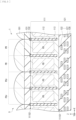
FIG. 2 illustrates an example of an arrangement of the light-receiving pixels P in thepixel array 11.FIG. 3 illustrates an example of an outline cross-sectional structure of thepixel array 11. It is to be noted thatFIG. 3 illustrates a cross-section corresponding to a line I-I' illustrated inFIG. 6 . Thepixel array 11 includes a plurality of pixel blocks 100 and a plurality oflenses 101. - The plurality of pixel blocks 100 includes pixel blocks 100R, 100Gr, 100Gb, and 100B. In the
pixel array 11, the plurality of light-receiving pixels P is arranged in minimum repeating units (units U) of the four pixel blocks 100 (the pixel blocks 100R, 100Gr, 100Gb, and 100B). - The
pixel block 100R includes, for example, eight light-receiving pixels P (light-receiving pixels PR) includingcolor filters 131 of red (R), for example. The pixel block 100Gr includes, for example, ten light-receiving pixels P (light-receiving pixels PGr) includingcolor filters 131 of green (G), for example. The pixel block 100Gb includes, for example, ten light-receiving pixels P (light-receiving pixels PGb) includingcolor filters 131 of green (G), for example. Thepixel block 100B includes, for example, eight light-receiving pixels P (light-receiving pixels PB) includingcolor filters 131 of blue (B), for example. InFIG. 2 , differences in the colors between the color filters are expressed with hatch patterns. An arrangement pattern of the light-receiving pixels PR in thepixel block 100R and an arrangement pattern of the light-receiving pixels PB in thepixel block 100B are the same as each other. An arrangement pattern of the light-receiving pixels PGr in the pixel block 100Gr and an arrangement pattern of the light-receiving pixels PGb in the pixel block 100Gb are the same as each other. - In the unit U, the pixel blocks 100R, 100Gr, 100Gb, and 100B are arranged in two rows × two columns, for example. Specifically, the
pixel block 100R and thepixel block 100B having the same arrangement pattern and the pixel block 100Gr and the pixel block 100Gb having the same arrangement pattern are arranged respectively on diagonal lines intersecting each other. As an example, the pixel block 100Gr is disposed on the upper left, thepixel block 100R is disposed on the upper right, thepixel block 100B is disposed on the lower left, and the pixel block 100Gb is disposed on the lower right. In such a manner, the pixel blocks 100R, 100Gr, 100Gb, and 100B are arranged in a so-called Bayer arrangement in units of pixel blocks 100. - Here, the light-receiving pixel P corresponds to a specific example of a "light-receiving pixel" in the present disclosure. A
pixel pair 90A corresponds to a specific example of a "first pixel pair" in the present disclosure. The pixel block 100 corresponds to a specific example of a "pixel block" in the present disclosure. For example, the pixel block 100Gr and the pixel block 100Gb each correspond to a specific example of a "first pixel block" in the present disclosure. For example, thepixel block 100R and thepixel block 100B each correspond to a specific example of a "second pixel block" in the present disclosure. Thelens 101 corresponds to a specific example of a "lens" in the present disclosure. - As illustrated in
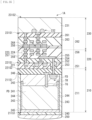
FIG. 3 , thepixel array 11 includes, for example, asemiconductor substrate 111, a light-receivingsection 112, apixel separation section 113, amultilayer wiring layer 121, thecolor filter 131, and a light-blockingfilm 132. - The
semiconductor substrate 111 is a support substrate to form theimaging device 1. Thesemiconductor substrate 111 is, for example, a P-type semiconductor substrate having a pair of surfaces (a front surface 111S1 and a back surface 111S2) opposed to each other. The light-receivingsection 112 is a semiconductor region formed to be embedded at a position corresponding to each of the plurality of light-receiving pixels P in the substrate of thesemiconductor substrate 111, in which a photodiode (PD) is formed by doping with N-type impurities, for example. Thepixel separation section 113 is provided at a boundary between the plurality of light-receiving pixels P adjacent to each other in an X-Y plane in the substrate of thesemiconductor substrate 111, and is, for example, a DTI (Deep Trench Isolation) configured using an insulating material such as an oxide film, for example. - The
multilayer wiring layer 121 is provided on the front surface 111S1 of thesemiconductor substrate 111, which is a surface opposite to a light incident side S of thepixel array 11. Themultilayer wiring layer 121 includes, for example, a plurality ofwiring layers 122 to 127 and an interlayer insulatinglayer 128. The plurality ofwiring layers 122 to 127 are provided in order from a side of the back surface 111S2 of thesemiconductor substrate 111. The plurality ofwiring layers 122 to 127 includes, for example, a plurality of transistors provided on the front surface 111S1 of thesemiconductor substrate 111 and a plurality of wiring lines such as a control line TRGL described later, for example, to couple thedrive section 12 and thereadout section 20 to each other. - The
color filter 131 is provided on theback surface 111 S2 of thesemiconductor substrate 111, which is the light incident side S of thepixel array 11. The light-blockingfilm 132 is provided, on the back surface 111S2 of thesemiconductor substrate 111, to surround two light-receiving pixels P (hereinafter, also referred to as thepixel pair 90A) adjacent to each other in an X-axis direction. - The plurality of
lenses 101 is each a so-called on-chip lens, and is provided on thecolor filters 131 on the light incident side S of thepixel array 11. Thelens 101 is provided over the two light-receiving pixels P (pixel pair 90A) adjacent to each other in the X-axis direction. Fourlenses 101 are provided over the eight light-receiving pixels P in thepixel block 100R. Fivelenses 101 are provided over the ten light-receiving pixels P in the pixel block 100Gr. Fivelenses 101 are provided over the ten light-receiving pixels P in the pixel block 100Gb. Fourlenses 101 are provided over the eight light-receiving pixels P in thepixel block 100B. Thelenses 101 are provided side by side in the X-axis direction and a Y-axis direction. Thelenses 101 side by side in the Y-axis direction are arranged to be shifted from each other in the X-axis direction by one light-receiving pixel P. In other words, the pixel pairs 90A side by side in the Y-axis direction are arranged to be shifted from each other in the X-axis direction by one light-receiving pixel P. - This configuration allows images to be shifted from each other in the two light-receiving pixels P in the
pixel pair 90A corresponding to onelens 101. Theimaging device 1 generates phase difference data DF on the basis of a so-called image-plane phase difference detected by the plurality of pixel pairs 90A. For example, a camera mounted with theimaging device 1 determines a defocus amount on the basis of the phase difference data DF, and moves the position of an imaging lens on the basis of this defocus amount. The camera is able to achieve autofocusing in such a manner. -
FIG. 4 illustrates a configuration example of the pixel block 100Gr.FIG. 5 illustrates a configuration example of thepixel block 100R. - The
pixel array 11 includes a plurality of control lines TRGL, a plurality of control lines RSTL, a plurality of control lines SELL, and a plurality of signal lines VSL. The control line TRGL corresponds to a specific example of a "control line" in the present disclosure. For example, the control lines TRGL extend in the X-axis direction (see, e.g.,FIGs. 16 to 18 ), and have respective one ends coupled to thedrive section 12. Thedrive section 12 supplies control signals STRG to the control lines TRGL. For example, the control lines RSTL extend in the X-axis direction (see, e.g.,FIG. 16 ), and have respective one ends coupled to thedrive section 12. Thedrive section 12 supplies control signals SRST to the control lines RSTL. For example, the control lines SELL extend in the X-axis direction (see, e.g.,FIG. 16 ), and have respective one ends coupled to thedrive section 12. Thedrive section 12 supplies control signals SSEL to the control lines SELL. For example, the signal lines VSL extend in the Y-axis direction (see, e.g.,FIG. 19 ), and have respective one ends coupled to thereadout section 20. The signal lines VSL transfer the signals SIG generated by the light-receiving pixels P to thereadout section 20. - The pixel block 100Gr (
FIG. 4 ) includes, for example, ten photodiodes, ten transistors TRG, five floating diffusion layers (FD), and one transistor RST, one transistor AMP and one transistor SEL, each as a pixel transistor. The ten photodiodes and the ten transistors TRG each respectively correspond to the ten light-receiving pixels PGr included in the pixel block 100Gr. The five floating diffusion layers are arranged one by one for the respective pixel pairs 90A. In other words, each of the five floating diffusion layers is shared by the two light-receiving pixels P constituting thepixel pair 90A and being adjacent to each other in the X-axis direction. The transistors TRG, RST, AMP, and SEL in this example are each an N-type MOS (Metal Oxide Semiconductor) transistor. The five floating diffusion layers and the transistors TRG, RST, AMP, and SEL are each provided on the front surface 111S1 of thesemiconductor substrate 111. - The photodiode is a photoelectric conversion element that generates electric charge in an amount corresponding to a received light amount and accumulates therein the generated electric charge. The photodiode has an anode grounded and a cathode coupled to a source of the transistor TRG.
- The transistor TRG transfers the electric charge generated by the photodiode to the floating diffusion layer. The transistor TRG has a gate coupled to the control line TRGL, the source coupled to the cathode of the photodiode, and a drain coupled to the floating diffusion layer. The gates of the ten transistors TRG are coupled to respective different control lines TRGL among the ten control lines TRGL (in this example, control lines TRGL1 to TRGL6 and TRGL9 to TRGL12).
- The floating diffusion layer is configured to accumulate the electric charge transferred from the photodiode via the transistor TRG. The floating diffusion layer is configured using, for example, a diffusion layer formed on a front surface of a semiconductor substrate.
- The transistor RST has a gate coupled to the control line RSTL, a drain to be supplied with a power supply voltage VDD, and a source coupled to the floating diffusion layer.
- The transistor AMP has a gate coupled to the floating diffusion layer, a drain to be supplied with the power supply voltage VDD, and a source coupled to a drain of the transistor SEL.
- The transistor SEL has a gate coupled to the control line SELL, the drain coupled to the source of the transistor AMP, and a source coupled to the signal line VSL.
- Here, the transistor TRG corresponds to a specific example of a "first transistor" in the present disclosure. The floating diffusion layer corresponds to a specific example of a "floating diffusion layer" of the present disclosure. The pixel transistor including the transistors RST, AMP, and SEL corresponds to a specific example of a "second transistor" of the present disclosure.
- With this configuration, in the light-receiving pixel P, for example, the electric charge accumulated in the photodiode is discharged by bringing the transistors TRG and RST each into an ON state on the basis of the control signals STRG and SRST. Then, an exposure period T is started by bringing the transistors TRG and RST each into an OFF state, and electric charge in an amount corresponding to a received light amount is thus accumulated in the photodiode. Then, after the exposure period T ends, the light-receiving pixel P outputs the signal SIG including a reset voltage Vreset and the pixel voltage Vpix to the signal line VSL. Specifically, first, the light-receiving pixel P is electrically coupled to the signal line VSL by bringing the transistor SEL into an ON state on the basis of the control signal SSEL. The transistor AMP is thereby coupled to a constant current source 21 (described later) of the
readout section 20, thus operating as a so-called source follower. Then, during a P-phase (Pre-Charge phase) period TP after the voltage of the floating diffusion layer is reset by bringing the transistor RST into an ON state, as described later, the light-receiving pixel P outputs a voltage corresponding to the voltage of the floating diffusion layer at that time as the reset voltage Vreset. Further, during a D-phase (Data phase) period TD after electric charge is transferred from the photodiode to the floating diffusion layer by bringing the transistor TRG into an ON state, the light-receiving pixel P outputs a voltage corresponding to the voltage of the floating diffusion layer at that time as the pixel voltage Vpix. A difference voltage between the pixel voltage Vpix and the reset voltage Vreset corresponds to a received light amount of the light-receiving pixel P during the exposure period T. In such a manner, the light-receiving pixel P outputs the signal SIG including the reset voltage Vreset and the pixel voltage Vpix to the signal line VSL. - The
pixel block 100R (FIG. 5 ) includes eight photodiodes, eight transistors TRG, four floating diffusion layers, and one transistor RST, one transistor AMP and one transistor SEL, each as a pixel transistor. The eight photodiodes and the eight transistors TRG each respectively correspond to the eight light-receiving pixels PR included in thepixel block 100R. The gates of the eight transistors TRG are coupled to respective different control lines TRGL among the eight control lines TRGL (in this example, the control lines TRGL1, TRGL2, and TRGL5 to TRGL10). In the same manner as the pixel block 100Gr, the four floating diffusion layers are arranged one by one for the respective pixel pairs 90A, and each of the four floating diffusion layers is shared by the two light-receiving pixels P constituting thepixel pair 90A and being adjacent to each other in the X-axis direction. The four floating diffusion layers and the transistors TRG, RST, AMP, and SEL are each provided on the front surface 111S1 of thesemiconductor substrate 111. - In the same manner as the pixel block 100R (
FIG. 5 ), thepixel block 100B includes eight photodiodes, eight transistors TRG, four floating diffusion layers, and one transistor RST, one transistor AMP and one transistor SEL, each as a pixel transistor. The eight photodiodes and the eight transistors TRG each respectively correspond to the eight light-receiving pixels PB included in thepixel block 100B. The gates of the eight transistors TRG are coupled to respective different control lines TRGL among the eight control lines TRGL. In the same manner as the pixel block 100Gr, the four floating diffusion layers are arranged one by one for the respective pixel pairs 90A, and each of the four floating diffusion layers is shared by the two light-receiving pixels P constituting thepixel pair 90A and being adjacent to each other in the X-axis direction. The four floating diffusion layers and the transistors TRG, RST, AMP, and SEL are each provided on thefront surface 111 S1 of thesemiconductor substrate 111. - In the same manner as the pixel block 100Gr (
FIG. 4 ), the pixel block 100Gb includes ten photodiodes, ten transistors TRG, five floating diffusion layers, and one transistor RST, one transistor AMP and one transistor SEL, each as a pixel transistor. The ten photodiodes and the ten transistors TRG each respectively correspond to the ten light-receiving pixels PGb included in the pixel block 100Gb. The gates of the ten transistors TRG are coupled to respective different control lines TRGL among the ten control lines TRGL. The five floating diffusion layers are arranged one by one for the respective pixel pairs 90A, and each of the five floating diffusion layers is shared by the two light-receiving pixels P constituting thepixel pair 90A and being adjacent to each other in the X-axis direction. The five floating diffusion layers and the transistors TRG, RST, AMP, and SEL are each provided on the front surface 111S1 of thesemiconductor substrate 111. -
FIG. 6 illustrates an example of a planar configuration in each of the plurality of light-receiving pixels P constituting the pixel blocks 100R, 100Gr, 100Gb, and 100B. - As described above, the five or four floating diffusion layers provided in each of the pixel blocks 100R, 100Gr, 100Gb, and 100B are shared by the two light-receiving pixels P constituting the
pixel pair 90A and being adjacent to each other in the X-axis direction. Specifically, as illustrated inFIG. 6 , the floating diffusion layer is disposed at a boundary between the two light-receiving pixels P constituting thepixel pair 90A and being adjacent to each other in the X-axis direction. - The ten or eight transistors TRG provided in each of the pixel blocks 100R, 100Gr, 100Gb, and 100B are provided one by one for the respective ten or eight light-receiving pixels P constituting each of the pixel blocks 100R, 100Gr, 100Gb, and 100B. For example, as illustrated in
FIG. 6 , the gates of the transistors TRG provided in the respective light-receiving pixels P are arranged to be opposed to each other along the X-axis direction, for each of the pixel pairs 90A, with the floating diffusion layer, which is arranged at the boundary between the two light-receiving pixels P adjacent to each other in the X-axis direction, being interposed therebetween. In addition, as illustrated inFIG. 6 , for example, one floating diffusion layer and the gates of the two transistors TRG arranged to be opposed to each other provided for each of the pixel pairs 90A are each arranged to be one-sided toward one (e.g., a lower side on the sheet) of a pair of sides opposed to each other in the Y-axis direction in each of the pixel pairs 90A. - It is to be noted that the positions of the one floating diffusion layer and the gates of the two transistors TRG arranged to be opposed to each other provided for each of the pixel pairs 90A are not limited thereto. For example, as illustrated in
FIG. 7 , the one floating diffusion layer and the gates of the two transistors TRG arranged to be opposed to each other provided for each of the pixel pairs 90A may be arranged to be one-sided toward one (e.g., a lower side on the sheet), of a pair of sides opposed to each other in the Y-axis direction, and toward the other (e.g., a lower side on the sheet) thereof, on every other row. - Further, as illustrated in
FIG. 6 , for example, the plurality of light-receiving pixels P constituting the pixel blocks 100R, 100Gr, 100Gb, and 100B are arranged cyclically in the Y-axis direction by using, as apixel pair 90B, two light-receiving pixels P adjacent to each other in the Y-axis direction. Further, two light-receiving pixels P adjacent to each other in the X-axis direction of the pixel pairs 90B mutually have a mirror image structure, as illustrated inFIG. 6 , for example. -
FIG. 8 illustrates an example of a planar arrangement of pixel transistors provided for each of the pixel blocks 100R, 100Gr, 100Gb, and 100B. - The pixel transistor includes the transistors RST, AMP, and SEL, and one transistor RST, one transistor AMP and one transistor SEL are provided for each of the pixel blocks 100R, 100Gr, 100Gb, and 100B. In other words, a unit U including the pixel blocks 100R, 100Gr, 100Gb, and 100B includes 12 pixel transistors (RST-R, RST-Gr, RST-Gb, RST-B, AMP-R, AMP-Gr, AMP-Gb, AMP-B, SEL-R, SEL-Gr, SEL-Gb, and SEL-B). It is to be noted that R, Gr, Gb, and B attached to the end of each symbol of the pixel transistors correspond to the pixel blocks 100R, 100Gr, 100Gb, and 100B in which the respective pixel transistors are provided. In a case where the respective pixel transistors provided in the pixel blocks 100R, 100Gr, 100Gb, and 100B need not be distinguished from one another, R, Gr, Gb, and B attached to the end thereof are omitted.
- The 12 pixel transistors are provided to be divided into three groups of four pixel transistors (e.g., [RST-Gr, RST-B/RST-R/RST-Gb]/ [AMP-Gr/SEL-Gr/SEL-R/AMP-R]/ [AMP-B/SEL-B/SEL-Gb/AMP-Gb]), for example. The four pixel transistors of each group are provided side by side, for example, along the X-axis direction. For example, as illustrated in
FIG. 7 , in a case where the one floating diffusion layer and the gates of the two transistors TRG arranged to be opposed to each other provided for each of the pixel pairs 90A are arranged to be one-sided toward one (e.g., a lower side on the sheet), of a pair of sides opposed to each other in the Y-axis direction, and toward the other side (e.g., a lower side on the sheet) thereof, on every other row, four pixel transistors of each group are provided side by side at the boundary between two light-receiving pixels P adjacent to each other in the Y-axis direction, as illustrated inFIG. 8 , for example. In such a manner, the four pixel transistors of each group at the boundary between two light-receiving pixels P adjacent to each other in the Y-axis direction are shared by the two light-receiving pixels P adjacent to each other in the Y-axis direction. This improves area efficiency. In addition, the four pixel transistors of each group are arranged cyclically in each of the X-axis direction and the Y-axis direction. A cycle in the X-axis direction is larger than a cycle in the Y-axis direction, and is twice larger, for example. -
Element separation sections element separation section 115 electrically separates adiffusion region 114 and the light-receivingsection 112 from each other. Thediffusion region 114, in which N-type impurities are diffused, is provided on the front surface 111S1 of thesemiconductor substrate 111 constituting the source/drain of the transistors TRG, RST, AMP, and SEL. Theelement separation section 116 electrically separates the plurality of pixel transistors provided side by side, as appropriate, from each other. Theelement separation sections semiconductor substrate 111. - In a case where the
element separation section 115 is configured by the STI, the floating diffusion layer is formed closer to theelement separation section 115 with respect to a line segment passing through the centers of the respective gates of the transistors TRG arranged to be opposed to each other along the X-axis direction, and the floating diffusion layer is brought into contact with the element separation section, for example, as illustrated inFIG. 9 . Intentionally avoiding injection of a P-type diffusion layer for securing STI pinning eliminates an electric field of a PN junction generated between the P-type diffusion layer and the floating diffusion layer (N-type diffusion layer), thus suppressing a white spot in the floating diffusion layer. It is to be noted that not securing the STI pinning results in generation of a dark current from the STI; however, by devising a potential design to block a path for the dark current to a deeper portion and to allow the dark current to flow to a side of the floating diffusion layer, the generated dark current is accumulated in the floating diffusion layer. A correlated double sampling (CDS) operation upon reading signal charge enables the dark current accumulated in the floating diffusion layer to be removed. In the same manner as the floating diffusion layer, a contact (floating diffusion layer contact) provided on the floating diffusion layer is also formed closer to theelement separation section 115 with respect to the line segment passing through the centers of the respective gates of the transistors TRG arranged to be opposed to each other along the axial direction. - In a case where the
element separation section 115 is configured by an impurity layer, the floating diffusion layer is disposed away from theelement separation section 115 with respect to the line segment passing through the centers of the respective gates of the transistors TRG arranged to be opposed to each other along the X-axis direction, for example, as illustrated inFIG. 10 . This relaxes an electric field generated between theelement separation section 115 and the floating diffusion layer, thus suppressing the floating diffusion layer having more white spots. In the same manner as the floating diffusion layer, a contact (floating diffusion layer contact) provided on the floating diffusion layer is also formed away from theelement separation section 115 with respect to the line segment passing through the centers of the respective gates of the transistors TRG arranged to be opposed to each other along the axial direction. - It is to be noted that the
element separation section 115 for separating the photodiode and the pixel transistor from each other is preferably formed using an impurity layer. This enables the dosing amount of P-type ions to be reduced, thus making it possible to further suppress the floating diffusion layer having more white spots, as compared with the case where theelement separation section 115 is formed as the STI. In addition, theelement separation section 116 between the pixel transistors of the adjacent light-receiving pixels P is preferably formed by the STI. This enables reduction in a space necessary for the separation, thus making it possible to extend a channel length and a gate width of the pixel transistor. - A well contact region WellCon for applying fixed electric charge to the
semiconductor substrate 111 may be provided between pixel transistors provided side by side for each of the pixel blocks 100R, 100Gr, 100Gb, and 100B. This makes it possible to reduce a surface electric field on the periphery of the light-receivingsection 112, as compared with the case of being disposed immediately below the light-receiving section 112 (lower side inFIG. 3 ). The well contact region WellCon corresponds to a specific example of a "substrate contact" of the present disclosure. In addition, thediffusion region 114 may be shared by pixel transistors provided side by side, for example, as illustrated inFIG. 11 . This makes it possible to reduce an area for the formation of pixel transistors. Further, a transistor FDG may be further provided in order to switch conversion efficiency. At that time, for example, as illustrated inFIG. 12 , the transistors AMP and SEL and the transistors RST and FDG are arranged in different rows in the pixel blocks 100Gr and 100Gb, and the transistors AMP, SEL, RST, and FDG are arranged in the same row in the pixel blocks 100R and 100B. This enables the control lines RSTL and FDGL of the transistors RST and FDG to be shared by thepixel block 100R and the pixel block 100Gr provided side by side in the X-axis direction and by the pixel block 100Gb and thepixel block 100B, thus making it possible to reduce the number of control wiring lines. It is to be noted that the transistor FDG corresponds to a specific example of the "second transistor" of the present disclosure, in the same manner as the transistors RST, AMP, and SEL. In addition, the arrangement of the pixel transistors illustrated inFIG. 12 is merely exemplary, and is not limited thereto. For example,FIG. 12 exemplifies the arrangement of the transistors SEL, AMP, RST, and FDG in the pixel blocks 100R and 100B as well as the arrangement of the transistors RST and FDG in the pixel blocks 100Gr and 100Gb. However, the transistors SEL, AMP, RST, and FDG may be arranged in the pixel blocks 100Gr and 100Gb, and the transistors RST and FDG may be arranged in the pixel blocks 100R and 100B. - Further, in the present embodiment, the plurality of floating diffusion layers, the gates of the plurality of transistors TRG, the plurality of pixel transistors (transistors RST, AMP, SEL, and FDG) provided for each of the pixel blocks 100R, 100Gr, 100Gb, and 100B, and various wiring lines (a plurality of coupling wiring lines FDL, the plurality of control lines TRGL, RSTL, and SELL, the plurality of signal lines VSL, a reference potential line VSS and a power supply line VDDL) provided in the unit U are each arranged point-symmetrically with respect to the center of the unit U.
-
FIG. 13 illustrates the plurality of floating diffusion layers, the gates of the plurality of transistors TRG, the plurality of pixel transistors (transistors RST, AMP, SEL, and FDG) provided for each of the pixel blocks 100R, 100Gr, 100Gb, and 100B provided on the front surface 111S1 of thesemiconductor substrate 111, together with outlines of the pixel blocks 100R, 100Gr, 100Gb, and 100B.FIG. 14 illustrates various wiring lines (coupling wiring lines FDL of a plurality of FDs, the plurality of control lines TRGL, RSTL, SELL, and FDGL, the plurality of signal lines VSL, the reference potential line VSS, and the power supply line VDDL) provided in thewiring layer 122, for example, together with the outlines of the pixel blocks 100R, 100Gr, 100Gb, and 100B.FIG. 15 illustrates various wiring lines (coupling wiring lines SubFDL of a plurality of SubFDs, the plurality of control lines TRGL, RSTL, SELL, and FDGL, the plurality of signal lines VSL, the reference potential line VSS, and the power supply line VDDL) provided in a wiring layer 123, for example, together with the outlines of the pixel blocks 100R, 100Gr, 100Gb, and 100B.FIG. 16 illustrates various wiring lines (the plurality of control lines TRGL, RSTL, and SELL, the plurality of signal lines VSL, the reference potential line VSS, and the power supply line VDDL) provided in the wiring layer 124, for example, together with the outlines of the pixel blocks 100R, 100Gr, 100Gb, and 100B.FIG. 17 illustrates various wiring lines (the plurality of control lines TRGL and FDGL, the plurality of signal lines VSL, the reference potential line VSS, and the power supply line VDDL) provided in the wiring layer 125, for example, together with the outlines of the pixel blocks 100R, 100Gr, 100Gb, and 100B.FIG. 18 illustrates various wiring lines (the plurality of control lines TRGL and FDGL, the plurality of signal lines VSL, the reference potential line VSS, and the power supply line VDDL) provided in the wiring layer 126, for example, together with the outlines of the pixel blocks 100R, 100Gr, 100Gb, and 100B.FIG. 19 illustrates various wiring lines (the plurality of signal lines VSL, the reference potential line VSS, and the power supply line VDDL) provided in thewiring layer 127, for example, together with the outlines of the pixel blocks 100R, 100Gr, 100Gb, and 100B. The plurality of floating diffusion layers, the gates of the plurality of transistors TRG, the plurality of pixel transistors (transistors RST, AMP, SEL, and FDG) provided for each of the pixel blocks 100R, 100Gr, 100Gb, and 100B, and various wiring lines provided in each of the wiring layers 122 to 127 (the plurality of coupling wiring lines FDL, the plurality of control lines TRGL, RSTL, SELL, and FDGL, the plurality of signal lines VSL, the reference potential line VSS, and the power supply line VDDL) provided on the front surface 111S1 of thesemiconductor substrate 111 are each arranged point-symmetrically with respect to the center (a symbol of a star in the drawing) of the unit U. - This allows the pixel block 100Gr and the pixel block 100Gb having the same arrangement pattern of the light-receiving pixels P and a pixel block R and a pixel block B having the same arrangement pattern of the light-receiving pixels P each have equivalent conversion efficiency. It is therefore possible to simplify a correction circuit in subsequent stage processing. In addition, capacity characteristics are also equivalent, thus making it possible to reduce dispersion of the characteristics.
- In the
wiring layer 122 including the coupling wiring line FDL that couples the four or five floating diffusion layers and the gates of the transistors AMP together in each of the pixel blocks 100R, 100Gr, 100Gb, and 100B, the plurality of control lines TRGL is provided to be along the coupling wiring line FDL, for example, as illustrated inFIG. 14 . This improves the coupling between the coupling wiring line FDL and the control line TRGL and suppresses the coupling between the coupling wiring line FDL and the plurality of other control lines RSTL, SELL, and FDGL as well as the plurality of signal lines VSL. This allows for an improvement in a transfer auxiliary effect by the control line TRGL. - The drive section 12 (
FIG. 1 ) is configured to drive the plurality of light-receiving pixels P in thepixel array 11 on the basis of instructions from theimaging control section 18. Specifically, thedrive section 12 drives the plurality of light-receiving pixels P in thepixel array 11 by supplying the plurality of control signals STRG respectively to the plurality of control lines TRGL, supplying the plurality of control signals SRST respectively to the plurality of control lines RSTL, and supplying the plurality of control signals SSEL respectively to the plurality of control lines SELL in thepixel array 11. - The reference
signal generation section 13 is configured to generate a reference signal RAMP on the basis of instructions from theimaging control section 18. The reference signal RAMP has a so-called ramp waveform in which a voltage level gradually changes with a lapse of time during periods during which thereadout section 20 performs AD conversion (the P-phase period TP and the D-phase period TD). The referencesignal generation section 13 supplies such a reference signal RAMP to thereadout section 20. - The
readout section 20 is configured to generate an image signal SpicO on the basis of instructions from theimaging control section 18 by performing AD conversion on the basis of the signal SIG supplied from thepixel array 11 via the signal line VSL. -
FIG. 20 illustrates a configuration example of thereadout section 20. It is to be noted thatFIG. 20 also illustrates the referencesignal generation section 13, thesignal processing section 15, and theimaging control section 18 in addition to thereadout section 20. Thereadout section 20 includes a plurality of constantcurrent sources 21, a plurality of AD (Analog to Digital) converters ADC, and atransfer controller 27. The plurality of constantcurrent sources 21 and the plurality of AD converters ADC are provided in correspondence with the plurality of respective signal lines VSL. In the following, a description is given of the constantcurrent source 21 and the AD converter ADC corresponding to one signal line VSL. - The constant
current source 21 is configured to feed a predetermined current through the corresponding signal line VSL. The constantcurrent source 21 has one end coupled to the corresponding signal line VSL and another end grounded. - The AD converter ADC is configured to perform AD conversion on the basis of the signal SIG on the corresponding signal line VSL. The AD converter ADC includes
capacitors counter 25, and a latch 26. - The
capacitor 22 has one end coupled to the signal line VSL and is to be supplied with the signal SIG, and another end coupled to the comparison circuit 24. Thecapacitor 23 has one end to be supplied with the reference signal RAMP supplied from the referencesignal generation section 13, and another end coupled to the comparison circuit 24. - The comparison circuit 24 is configured to generate a signal CP by performing comparison operations on the basis of the signal SIG supplied from the light-receiving pixel P via the signal line VSL and the
capacitor 22 and the reference signal RAMP supplied from the referencesignal generation section 13 via thecapacitor 23. The comparison circuit 24 sets an operating point by setting voltages of thecapacitors imaging control section 18. In addition, the comparison circuit 24 thereafter performs a comparison operation of comparing the reset voltage Vreset included in the signal SIG and the voltage of the reference signal RAMP during the P-phase period TP, and performs a comparison operation of comparing the pixel voltage Vpix included in the signal SIG and the voltage of the reference signal RAMP during the D-phase period TD. - The
counter 25 is configured to perform a counting operation of counting pulses of a clock signal CLK supplied from theimaging control section 18 on the basis of the signal CP supplied from the comparison circuit 24. Specifically, during the P-phase period TP, thecounter 25 generates a count value CNTP by counting the pulses of the clock signal CLK until the signal CP transitions, and outputs the count value CNTP as a digital code having a plurality of bits. In addition, during the D-phase period TD, thecounter 25 generates a count value CNTD by counting the pulses of the clock signal CLK until the signal CP transitions, and outputs the count value CNTD as a digital code having a plurality of bits. - The latch 26 is configured to temporarily hold the digital codes supplied from the
counter 25 and to output the digital codes to a bus wiring line BUS on the basis of instructions from thetransfer controller 27. - The
transfer controller 27 is configured to perform control on the basis of a control signal CTL supplied from theimaging control section 18 to cause the latches 26 of the plurality of AD converters ADC to sequentially output the digital codes to the bus wiring line BUS. Thereadout section 20 uses this bus wiring line BUS to sequentially transfer, as the image signals SpicO, the plurality of digital codes supplied from the plurality of AD converters ADC to thesignal processing section 15. - The signal processing section 15 (
FIG. 1 ) is configured to generate an image signal Spic by performing predetermined signal processing on the basis of the image signal SpicO and instructions from theimaging control section 18. Thesignal processing section 15 includes animage data generator 16 and a phasedifference data generator 17. Theimage data generator 16 is configured to generate image data DP representing a captured image by performing predetermined image processing on the basis of the image signal SpicO. The phasedifference data generator 17 is configured to generate phase difference data DF representing an image-plane phase difference by performing predetermined image processing on the basis of the image signal SpicO. Thesignal processing section 15 generates the image signal Spic including the image data DP generated by theimage data generator 16 and the phase difference data DF generated by the phasedifference data generator 17. -
FIG. 21 illustrates an example of the image signal Spic. Thesignal processing section 15 generates the image signal Spic by, for example, alternately arranging the image data DP for a plurality of rows of light-receiving pixels P and the phase difference data DF for a plurality of rows of light-receiving pixels P. Thesignal processing section 15 then outputs such an image signal Spic. - The
imaging control section 18 is configured to control the operation of theimaging device 1 by supplying control signals to thedrive section 12, the referencesignal generation section 13, thereadout section 20, and thesignal processing section 15 and controlling the operations of these circuits. Theimaging control section 18 is to be supplied with a control signal Sctl from an external source. The control signal Sctl includes, for example, information about a zoom factor of a so-called electronic zoom. Theimaging control section 18 controls the operation of theimaging device 1 on the basis of the control signal Sctl. - Subsequently, a description is given of the operations and workings of the
imaging device 1 according to the present embodiment. - First, an overview of an overall operation of the
imaging device 1 is described with reference toFIGs. 1 and20 . Thedrive section 12 subsequentially drives the plurality of light-receiving pixels P in thepixel array 11 on the basis of instructions from theimaging control section 18. The referencesignal generation section 13 generates the reference signal RAMP on the basis of instructions from theimaging control section 18. The light-receiving pixel P outputs the reset voltage Vreset as the signal SIG during the P-phase period TP, and outputs the pixel voltage Vpix corresponding to a received light amount as the signal SIG during the D-phase period TD. Thereadout section 20 generates the image signal SpicO on the basis of the signal SIG supplied from thepixel array 11 via the signal line VSL and instructions from theimaging control section 18. In thesignal processing section 15, theimage data generator 16 generates the image data DP representing a captured image by performing predetermined image processing on the basis of the image signal SpicO, and the phasedifference data generator 17 generates the phase difference data DF representing the image-plane phase difference by performing predetermined image processing on the basis of the image signal SpicO. Then, thesignal processing section 15 generates the image signal Spic including the image data DP and the phase difference data DF. Theimaging control section 18 controls the operation of theimaging device 1 by supplying control signals to thedrive section 12, the referencesignal generation section 13, thereadout section 20, and thesignal processing section 15 and controlling the operations of these circuits. - The
imaging control section 18 controls the operation of theimaging device 1 on the basis of the control signal Sctl including the information about the zoom factor of the electronic zoom. A description is given below of a zoom operation of theimaging device 1. -
FIG. 22 illustrates an example of the number of the light-receiving pixels P pertaining to a captured image (the number of effective pixels) in a case where the zoom factor is varied from 1x to 10x. InFIG. 22 , the solid line represents the number of effective pixels of theimaging device 1.FIG. 23 illustrates an example of the zoom operation of theimaging device 1, in which (A) illustrates an operation in a case where the zoom factor is 1x, (B) illustrates an operation in a case where the zoom factor is 2x, and (C) illustrates an operation in a case where the zoom factor is 3x. - The
imaging device 1 has three imaging modes M (imaging modes MA, MB, and MC). Theimaging control section 18 selects one of the three imaging modes MA to MC on the basis of the information about the zoom factor included in the control signal Sctl. Specifically, as illustrated inFIG. 22 , theimaging control section 18 selects the imaging mode MA in a case where the zoom factor is less than 2, selects the imaging mode MB in a case where the zoom factor is 2 or more and less than 3, and selects the imaging mode MC in a case where the zoom factor is 3 or more. - In the imaging mode MA, as illustrated in (A) of
FIG. 23 , theimaging device 1 obtains four pixel values V (pixel values VR, VGr, VGb, and VB) for each of a plurality of units or units U. Specific operations are described later. In such a manner, theimaging device 1 generates the image data DP by generating the pixel values V with a ratio of four pixel values V to 36 light-receiving pixels P. In a case where the number of the light-receiving pixels P in thepixel array 11 is 108 [Mpix], the pixel values V are calculated for 12 [Mpix]. Thus, as illustrated inFIG. 22 , the number of effective pixels is 12 [Mpix]. - As illustrated in
FIG. 22 , when the zoom factor is increased from one in the imaging mode MA, the number of effective pixels decreases in accordance with the factor. Then, when the zoom factor reaches two, the imaging mode M turns into the imaging mode MB. - In the imaging mode MB, as illustrated in (B) of
FIG. 23 , theimaging device 1 obtains 16 pixel values V for each of the plurality of units or units U. Specific operations are described later. In such a manner, theimaging device 1 generates the image data DP by generating the pixel values V with a ratio of 16 pixel values V to 36 light-receiving pixels P. In the case where the number of the light-receiving pixels Pin thepixel array 11 is 108 [Mpix], the pixel values V are calculated for 48 [Mpix]. In actuality, because the zoom factor is 2x, the imaging region is reduced to 1/4 as illustrated in (B) ofFIG. 23 , and the number of effective pixels is thus 12 [Mpix] (= 48 [Mpix]/4). - As illustrated in
FIG. 22 , when the zoom factor is increased from two in the imaging mode MB, the number of effective pixels decreases in accordance with the factor. Then, when the zoom factor reaches three, the imaging mode M turns into the imaging mode MC. - In the imaging mode MC, as illustrated in (C) of
FIG. 23 , theimaging device 1 obtains 36 pixel values V for each of the plurality of units or units U. Specific operations are described later. In such a manner, theimaging device 1 generates the image data DP by generating the pixel values V with a ratio of 36 pixel values V to 36 light-receiving pixels P. In the case where the number of the light-receiving pixels P in thepixel array 11 is 108 [Mpix], it is possible to obtain a captured image of 108 [Mpix]. In actuality, because the zoom factor is 3x, the imaging region is reduced to 1/9 as illustrated in (C) ofFIG. 23 , and the number of effective pixels is thus 12 [Mpix] (= 108 [Mpix]/9). - As described above, the
imaging device 1 is provided with the three imaging modes M, and it is therefore possible to reduce a change in the image quality of a captured image in a case where the zoom factor is changed. That is, for example, in a case where the imaging mode MB is omitted and the two the imaging modes MA and MC are provided, selecting the imaging mode MA in a case where the zoom factor is less than 2x and selecting the imaging mode MC in a case where the zoom factor is 2x or more result in a large change in the number of effective pixels, as illustrated in broken lines inFIG. 22 . That is, in this example, in a case where the zoom factor is 2x, the imaging mode MC is selected, and the number of effective pixels is 27 [Mpix] (= 108 [Mpix]/4). Therefore, a large difference occurs between the number of effective pixels in a case where the zoom factor is, for example, 1.9x and the number of effective pixels in the case where the zoom factor is 2x. This can result in a large change in the image quality of a captured image at a zoom factor of around 2x. In contrast, theimaging device 1 is provided with the three imaging modes M, and is thus able to reduce a change in the number of effective pixels in the case of changing the zoom factor. This makes it possible to suppress a change in the image quality of a captured image. -
FIG. 24 illustrates an operation example of theimaging device 1 in the imaging mode MA. InFIG. 24 , the light-receiving pixels P illustrated with "o" represent the light-receiving pixels P that are targeted for the readout operation. - First, as illustrated in (A) of
FIG. 24 , theimaging device 1 generates image data DT1 by calculating a pixel value V corresponding to a received light amount of the left light-receiving pixels P in the pixel pairs 90A provided with thelenses 101 in each of the plurality of pixel blocks 100. Specifically, among the ten light-receiving pixels PGr in the pixel block 100Gr, theimaging device 1 targets the five light-receiving pixels PGr arranged on the left in the fivepixel pairs 90A for the readout operation, and thus calculates a pixel value VGr1 at a centroid position of the five light-receiving pixels PGr. In addition, among the eight light-receiving pixels PR in thepixel block 100R, theimaging device 1 targets the four light-receiving pixels PR arranged on the left in the fourpixel pairs 90A for the readout operation, and thus calculates a pixel value VR1 at a centroid position of the four light-receiving pixels PR. Among the eight light-receiving pixels PB in thepixel block 100B, theimaging device 1 targets the four light-receiving pixels PB arranged on the left in the fourpixel pairs 90A for the readout operation, and thus calculates a pixel value VB1 at a centroid position of the four light-receiving pixels PB. Among the ten light-receiving pixels PGb in the pixel block 100Gb, theimaging device 1 targets the five light-receiving pixels PGb arranged on the left in the fivepixel pairs 90A for the readout operation, and thus calculates a pixel value VGb1 at a centroid position of the five light-receiving pixels PGb. In such a manner, theimaging device 1 generates the image data DT1 ((A) ofFIG. 24 ) including the pixel values VGr1, VR1, VB1, and VGb1. - Next, as illustrated in (B) of
FIG. 24 , theimaging device 1 generates image data DT2 by calculating pixel values V corresponding to received light amounts of all of the light-receiving pixels P in each of the plurality of pixel blocks 100. Specifically, theimaging device 1 targets the ten light-receiving pixels PGr in the pixel block 100Gr for the readout operation, and thus calculates a pixel value VGr2 at a centroid position of the ten light-receiving pixels PGr. Further, theimaging device 1 targets the eight light-receiving pixels PR in thepixel block 100R for the readout operation, and thus calculates a pixel value VR2 at a centroid position of the eight light-receiving pixels PR. Theimaging device 1 targets the eight light-receiving pixels PB in thepixel block 100B for the readout operation, and thus calculates a pixel value VB2 at a centroid position of the eight light-receiving pixels PB. Theimaging device 1 targets the ten light-receiving pixels PGb in the pixel block 100Gb for the readout operation, and thus calculates a pixel value VGb2 at a centroid position of the ten light-receiving pixels PGb. In such a manner, theimaging device 1 generates the image data DT2 ((B) ofFIG. 24 ) including the pixel values VGr2, VR2, VB2, and VGb2. - With attention focused on the certain pixel block 100Gr, a description is given below of the readout operation on the ten light-receiving pixels PGr in the pixel block 100Gr.
-
FIG. 25 illustrates an example of the readout operation, in which (A) illustrates a waveform of the control signal SSEL, (B) illustrates a waveform of the control signal SRST, (C) illustrates a waveform of the control signal STRG (a control signal STRGL) supplied to the light-receiving pixel PGr arranged on the left in thepixel pair 90A, (D) illustrates a waveform of the control signal STRG (a control signal STRGR) supplied to the light-receiving pixel PGr arranged on the right in thepixel pair 90A, (E) illustrates a waveform of the control signal AZ, (F) illustrates a waveform of the reference signal RAMP, (G) illustrates a waveform of the signal SIG, and (H) illustrates a waveform of the signal CP. In (F) and (G) ofFIG. 25 , the waveforms of the reference signal RAMP and the signal SIG are illustrated using the same voltage axis. In addition, in this description, the waveform of the reference signal RAMP illustrated in (F) ofFIG. 25 is the waveform of a voltage supplied to an input terminal of the comparison circuit 24 via thecapacitor 23, and the waveform of the signal SIG illustrated in (G) ofFIG. 25 is the waveform of a voltage supplied to the input terminal of the comparison circuit 24 via thecapacitor 22. - First, a horizontal period H starts at a timing t11. The
drive section 12 thus changes the voltage of the control signal SSEL from the low level to the high level ((A) ofFIG. 25 ). This brings the transistor SEL into an ON state in the pixel block 100Gr, and causes the pixel block 100Gr to be electrically coupled to the signal line VSL. In addition, at this timing t11, thedrive section 12 changes the voltage of the control signal SRST from the low level to the high level ((B) ofFIG. 25 ). This brings the transistor RST into an ON state in the pixel block 100Gr, and causes the voltage of the floating diffusion layer to be set to the power supply voltage VDD (a reset operation). Then, the pixel block 100Gr outputs a voltage corresponding to the voltage of the floating diffusion layer at this time. In addition, at this timing t11, theimaging control section 18 changes the voltage of the control signal AZ from the low level to the high level ((E) ofFIG. 25 ). This causes the comparison circuit 24 of the AD converter ADC to set the operating point by setting the voltages of thecapacitors FIG. 25 ). - Then, at a timing at which a predetermined time has elapsed from the timing t11, the
drive section 12 changes the voltage of the control signal SRST from the high level to the low level ((B) ofFIG. 25 ). This brings the transistor RST into an OFF state in the pixel block 100Gr, and causes the reset operation to end. - Next, at a timing t12, the
imaging control section 18 changes the voltage of the control signal AZ from the high level to the low level ((E) ofFIG. 25 ). This causes the comparison circuit 24 to end the setting of the operating point. - Further, at this timing t12, the reference
signal generation section 13 sets the voltage of the reference signal RAMP to a voltage V1 ((F) ofFIG. 25 ). This makes the voltage of the reference signal RAMP higher than the voltage of the signal SIG. The comparison circuit 24 thus changes the voltage of the signal CP from the low level to the high level ((H) ofFIG. 25 ). - Then, during a period from a timing t13 to a timing 115 (P-phase period TP), the AD converter ADC performs AD conversion on the basis of the signal SIG. Specifically, first, at the timing t13, the reference
signal generation section 13 starts decreasing the voltage of the reference signal RAMP from the voltage V1 at a predetermined change rate ((F) ofFIG. 25 ). In addition, at this timing t13, theimaging control section 18 starts generating the clock signal CLK. Thecounter 25 of the AD converter ADC performs the counting operation to thereby count the pulses of the clock signal CLK. - Then, at a timing t14, the voltage of the reference signal RAMP falls below the voltage of the signal SIG (the reset voltage Vreset) ((F) and (G) of
FIG. 25 ). The comparison circuit 24 of the AD converter ADC thus changes the voltage of the signal CP from the high level to the low level ((H) ofFIG. 25 ). Thecounter 25 of the AD converter ADC stops the counting operation on the basis of the transition of the signal CP. The count value (count value CNTP) of thecounter 25 at this time is a value corresponding to the reset voltage Vreset. The latch 26 holds this count value CNTP. Thecounter 25 then resets the count value. - Next, at the timing t15, the
imaging control section 18 stops generating the clock signal CLK at the end of the P-phase period TP. In addition, the referencesignal generation section 13 stops changing the voltage of the reference signal RAMP at this timing 115 ((F) ofFIG. 25 ). Then, during a period from the timing t15 forward, thereadout section 20 supplies, as the image signal SpicO, the count value CNTP held by the latch 26 to thesignal processing section 15. - Next, at a timing t16, the
imaging control section 18 sets the voltage of the reference signal RAMP to the voltage V1 ((F) ofFIG. 25 ). This makes the voltage of the reference signal RAMP higher than the voltage of the signal SIG (the reset voltage Vreset). The comparison circuit 24 thus changes the voltage of the signal CP from the low level to the high level ((H) ofFIG. 25 ). - Next, at a timing t17, the
drive section 12 changes the voltage of the control signal STRGL from the low level to the high level ((C) ofFIG. 25 ). This brings the transistors TRG into an ON state in the five light-receiving pixels PGr arranged on the left in the pixel pairs 90A, and causes the electric charge generated at the photodiodes to be transferred to the floating diffusion layer (an electric charge transfer operation). Then, the pixel block 100Gr outputs a voltage corresponding to the voltage of the floating diffusion layer at this time. In such a manner, the voltage of the signal SIG becomes a pixel voltage Vpix1 ((G) ofFIG. 25 ). - Then, at a timing at which a predetermined time has elapsed from the timing t17, the
drive section 12 changes the voltage of the control signal STRGL from the high level to the low level ((C) ofFIG. 25 ). This brings the transistors TRG into an OFF state in the five light-receiving pixels PGr arranged on the left in the pixel pairs 90A, and causes the electric charge transfer operation to end. - Then, during a period from a timing 118 to a timing t20 (D-phase period TD1), the AD converter ADC performs AD conversion on the basis of the signal SIG. Specifically, first, at the timing t18, the reference
signal generation section 13 starts decreasing the voltage of the reference signal RAMP from the voltage V1 at a predetermined change rate ((F) ofFIG. 25 ). In addition, at this timing t18, theimaging control section 18 starts generating the clock signal CLK. Thecounter 25 of the AD converter ADC performs the counting operation to thereby count the pulses of the clock signal CLK. - Then, at a timing t19, the voltage of the reference signal RAMP falls below the voltage of the signal SIG (the pixel voltage Vpix1) ((F) and (G) of
FIG. 25 ). The comparison circuit 24 of the AD converter ADC thus changes the voltage of the signal CP from the high level to the low level ((H) ofFIG. 25 ). Thecounter 25 of the AD converter ADC stops the counting operation on the basis of the transition of the signal CP. The count value (count value CNTD1) of thecounter 25 at this time is a value corresponding to the pixel voltage Vpix1. The latch 26 holds this count value CNTD1. Thecounter 25 then resets the count value. - Next, at the timing t20, the
imaging control section 18 stops generating the clock signal CLK at the end of the D-phase period TD1. In addition, the referencesignal generation section 13 stops changing the voltage of the reference signal RAMP at this timing t20 ((F) ofFIG. 25 ). Then, during a period from the timing t20 forward, thereadout section 20 supplies, as the image signal SpicO, the count value CNTD1 held by the latch 26 to thesignal processing section 15. - Next, at a timing t21, the
imaging control section 18 sets the voltage of the reference signal RAMP to the voltage V1 ((F) ofFIG. 25 ). This makes the voltage of the reference signal RAMP higher than the voltage of the signal SIG (the pixel voltage Vpix1). The comparison circuit 24 thus changes the voltage of the signal CP from the low level to the high level ((H) ofFIG. 25 ). - Next, at a timing t22, the
drive section 12 changes the respective voltages of the control signals STRGL and STRGR from the low level to the high level ((C) and (D) ofFIG. 25 ). This brings the transistors TRG into an ON state in the ten light-receiving pixels PGr in the pixel block 100Gr, and causes the electric charge generated at the photodiodes to be transferred to the floating diffusion layer (the electric charge transfer operation). Then, the pixel block 100Gr outputs a voltage corresponding to the voltage of the floating diffusion layer at this time. In such a manner, the voltage of the signal SIG becomes a pixel voltage Vpix2 ((G) ofFIG. 25 ). - Then, at a timing at which a predetermined time has elapsed from the timing t22, the
drive section 12 changes the respective voltages of the control signals STRGL and STRGR from the high level to the low level ((C) and (D) ofFIG. 25 ). This brings the transistors TRG into an OFF state in the ten light-receiving pixels PGr, and causes the electric charge transfer operation to end. - Then, during a period from a timing t23 to a timing t25 (D-phase period TD2), the AD converter ADC performs AD conversion on the basis of the signal SIG. Specifically, first, at the timing t23, the reference
signal generation section 13 starts decreasing the voltage of the reference signal RAMP from the voltage V1 at a predetermined change rate ((F) ofFIG. 25 ). In addition, at this timing t23, theimaging control section 18 starts generating the clock signal CLK. Thecounter 25 of the AD converter ADC performs the counting operation to thereby count the pulses of the clock signal CLK. - Then, at a timing t24, the voltage of the reference signal RAMP falls below the voltage of the signal SIG (the pixel voltage Vpix2) ((F) and (G) of
FIG. 25 ). The comparison circuit 24 of the AD converter ADC thus changes the voltage of the signal CP from the high level to the low level ((H) ofFIG. 25 ). Thecounter 25 of the AD converter ADC stops the counting operation on the basis of the transition of the signal CP. The count value (count value CNTD2) of thecounter 25 at this time is a value corresponding to the pixel voltage Vpix2. The latch 26 holds this count value CNTD2. Thecounter 25 then resets the count value. - Next, at the timing t25, the
imaging control section 18 stops generating the clock signal CLK at the end of the D-phase period TD2. In addition, the referencesignal generation section 13 stops changing the voltage of the reference signal RAMP at this timing t25 ((F) ofFIG. 25 ). Then, during a period from the timing t25 forward, thereadout section 20 supplies, as the image signal SpicO, the count value CNTD2 held by the latch 26 to thesignal processing section 15. - Next, at a timing t26, the
drive section 12 changes the voltage of the control signal SSEL from the high level to the low level ((A) ofFIG. 25 ). This brings the transistor SEL into an OFF state in the pixel block 100Gr, and causes the pixel block 100Gr to be electrically decoupled from the signal line VSL. - In such a manner, the
readout section 20 supplies the image signal SpicO including the count values CNTP, CNTD1, and CNTD2 to thesignal processing section 15. Thesignal processing section 15 generates the pixel value VGr1 illustrated in (A) ofFIG. 24 and the pixel value VGr2 illustrated in (B) ofFIG. 24 by utilizing the principle of correlated double sampling on the basis of the count values CNTP, CNTD1, and CNTD2 included in the image signals SpicO, for example. Specifically, thesignal processing section 15 generates the pixel value VGr1 by, for example, subtracting the count value CNTP from the count value CNTD1. Because the count value CNTD1 is a value corresponding to the sum of received light amounts at the five light-receiving pixels PGr arranged on the left in the fivepixel pairs 90A in the pixel block 100Gr, thesignal processing section 15 is able to generate the pixel value VGr1 illustrated in (A) ofFIG. 24 on the basis of the count value CNTD1. Likewise, thesignal processing section 15 generates the pixel value VGr2 by, for example, subtracting the count value CNTP from the count value CNTD2. Because the count value CNTD2 is a value corresponding to the sum of received light amounts at the ten light-receiving pixels PGr in the pixel block 100Gr, thesignal processing section 15 is able to generate the pixel value VGr2 illustrated in (B) ofFIG. 24 on the basis of the count value CNTD2. - Although the description has been given above of the pixel block 100Gr, the same applies to the pixel blocks 100R, 100Gb, and 100B. In such a manner, as illustrated in
FIG. 24 , thesignal processing section 15 generates the image data DT1 including the pixel values VR1, VGr1, VGb1, and VB1 and the image data DT2 including the pixel values VR2, VGr2, VGb2, and VB2. -
FIG. 26 illustrates an example of image processing by thesignal processing section 15 in the imaging mode MA. - First, the
signal processing section 15 generates image data DT3 by performing subtraction processing on the basis of the image data DT1 and DT2. - Specifically, the
signal processing section 15 subtracts the pixel value VGr1 in the image data DT1 from the pixel value VGr2 in the image data DT2 to thereby calculate a pixel value VGr3. The pixel value VGr3 is a value corresponding to the sum of received light amounts at the five light-receiving pixels PGr arranged on the right in the fivepixel pairs 90A in the pixel block 100Gr. That is, the pixel value VGr1 is a value corresponding to the sum of received light amounts at the five light-receiving pixels PGr arranged on the left in the fivepixel pairs 90A in the pixel block 100Gr, and the pixel value VGr2 is a value corresponding to the sum of received light amounts at the ten light-receiving pixels PGr in the pixel block 100Gr. Therefore, subtracting the pixel value VGr1 from the pixel value VGr2 gives a value corresponding to the sum of received light amounts at the five light-receiving pixels PGr arranged on the right in the fivepixel pairs 90A in the pixel block 100Gr. Because the pixel value VGr3 is the value corresponding to the sum of received light amounts at the five light-receiving pixels PGr arranged on the right in the fivepixel pairs 90A as described above, the pixel value VGr3 is arranged at a centroid position of these five light-receiving pixels PGr, as illustrated inFIG. 26 . - Likewise, the
signal processing section 15 subtracts the pixel value VR1 in the image data DT1 from the pixel value VR2 in the image data DT2 to thereby calculate a pixel value VR3. The pixel value VR3 is a value corresponding to the sum of received light amounts at the four light-receiving pixels PR arranged on the right in the fourpixel pairs 90A in thepixel block 100R. The pixel value VR3 is arranged at a centroid position of the four light-receiving pixels PR arranged on the right in the fourpixel pairs 90A in thepixel block 100R. - The
signal processing section 15 subtracts the pixel value VB1 in the image data DT1 from the pixel value VB2 in the image data DT2 to thereby calculate a pixel value VB3. The pixel value VB3 is a value corresponding to the sum of received light amounts at the four light-receiving pixels PB arranged on the right in the fourpixel pairs 90A in thepixel block 100B. The pixel value VB3 is arranged at a centroid position of the four light-receiving pixels PB arranged on the right in the fourpixel pairs 90A in thepixel block 100B. - The
signal processing section 15 subtracts the pixel value VGb1 in the image data DT1 from the pixel value VGb2 in the image data DT2 to thereby calculate a pixel value VGb3. The pixel value VGb3 is a value corresponding to the sum of received light amounts at the five light-receiving pixels PGb arranged on the right in the fivepixel pairs 90A in the pixel block 100Gb. The pixel value VGb3 is arranged at a centroid position of the five light-receiving pixels PGb arranged on the right in the fivepixel pairs 90A in the pixel block 100Gb. - Then, the
image data generator 16 of thesignal processing section 15 performs predetermined image processing on the basis of the image data DT2 to thereby generate the image data DP ((A) ofFIG. 23 ) representing the captured image. - In addition, the phase
difference data generator 17 of thesignal processing section 15 performs predetermined image processing on the basis of the image data DT1 and DT3 to thereby generate the phase difference data DF representing the image-plane phase difference. That is, the image data DT1 includes the pixel values V at the light-receiving pixels P arranged on the left in the plurality of pixel pairs 90A, and the image data DT3 includes the pixel values V at the light-receiving pixels P arranged on the right in the plurality of pixel pairs 90A. The phasedifference data generator 17 is therefore able to generate the phase difference data DF on the basis of the image data DT1 and DT3. - In the
imaging device 1, as illustrated inFIG. 2 , thelenses 101 are provided side by side in the X-axis direction and the Y-axis direction in thepixel array 11. This makes it possible to generate the phase difference data DF at high resolution across the entire surface of thepixel array 11. Therefore, for example, a camera mounted with such animaging device 1 is able to achieve highly accurate autofocusing and, as a result, is able to increase image quality. - Here, the imaging mode MA corresponds to a specific example of a "first imaging mode" in the present disclosure. The pixel value in the image data DT1 corresponds to a specific example of a "first pixel value" in the present disclosure. The pixel value in the image data DT2 corresponds to a specific example of a "second pixel value" in the present disclosure. The pixel value in the image data DT3 corresponds to a specific example of a "third pixel value" in the present disclosure.
-
FIG. 27 illustrates an operation example of theimaging device 1 in the imaging mode MB.FIG. 28 more specifically illustrates the operation illustrated inFIG. 27 . InFIGs. 27 and15 , the light-receiving pixels P illustrated with "o" represent the light-receiving pixels P that are targeted for the readout operation. - In the pixel block 100Gr, as illustrated in (A) of
FIG. 28 , theimaging device 1 targets the light-receiving pixel PGr arranged on the left in onepixel pair 90A among the fivepixel pairs 90A in the pixel block 100Gr for the readout operation, and calculates the pixel value VGr1 at the position of this light-receiving pixel PGr. Then, as illustrated in (B) ofFIG. 28 , theimaging device 1 next targets the two light-receiving pixels PGr in thepixel pair 90A for the readout operation, and calculates the pixel value VGr2 at a centroid position of the two light-receiving pixels PGr. - Likewise, in the
pixel block 100R, as illustrated in (A) ofFIG. 28 , theimaging device 1 targets the light-receiving pixel PR arranged on the left in onepixel pair 90A among the fourpixel pairs 90A in thepixel block 100R for the readout operation, and calculates the pixel value VR1 at the position of this light-receiving pixel PR. Then, as illustrated in (B) ofFIG. 28 , theimaging device 1 next targets the two light-receiving pixels PR in thepixel pair 90A for the readout operation, and calculates the pixel value VR2 at a centroid position of the two light-receiving pixels PR. - Likewise, in the
pixel block 100B, as illustrated in (A) ofFIG. 28 , theimaging device 1 targets the light-receiving pixel PB arranged on the left in onepixel pair 90A among the fourpixel pairs 90A in thepixel block 100B for the readout operation, and calculates the pixel value VB1 at the position of this light-receiving pixel PB. Then, as illustrated in (B) ofFIG. 28 , theimaging device 1 next targets the two light-receiving pixels PB in thepixel pair 90A for the readout operation, and calculates the pixel value VB2 at a centroid position of the two light-receiving pixels PB. - Likewise, in the pixel block 100Gb, as illustrated in (A) of
FIG. 28 , theimaging device 1 targets the light-receiving pixel PGb arranged on the left in onepixel pair 90A among the fivepixel pairs 90A in the pixel block 100Gb for the readout operation, and calculates the pixel value VGb1 at the position of this light-receiving pixel PGb. Then, as illustrated in (B) ofFIG. 28 , theimaging device 1 next targets the two light-receiving pixels PGb in thepixel pair 90A for the readout operation, and calculates the pixel value VGb2 at a centroid position of the two light-receiving pixels PGb. - The readout operations in (A) and (B) of
FIG. 28 are operations similar to the readout operations in the imaging mode MA (FIG. 25 ) described above. Theimaging device 1 thereafter performs operations of (C) and (D) ofFIG. 28 , operations of (E) and (F) ofFIG. 28 , operations of (G) and (H) ofFIG. 28 , operations of (I) and (J) ofFIG. 28 , and operations of (K) and (L) ofFIG. 28 . In such a manner, theimaging device 1 generates the image data DT1 ((A) ofFIG. 27 ) including the pixel values VGr1, VR1, VB1, andVGb 1 and the image data DT2 ((B) ofFIG. 27 ) including the pixel values VGr2, VR2, VB2, and VGb2. -
FIG. 29 illustrates an example of image processing by thesignal processing section 15 in the imaging mode MB. - First, the
signal processing section 15 generates the image data DT3 by performing subtraction processing on the basis of the image data DT1 and DT2. - Specifically, the
signal processing section 15 subtracts the five pixel values VGr1 in the image data DT1 respectively from the five pixel values VGr2 in the image data DT2 to thereby calculate five pixel values VGr3. This pixel value VGr3 is a value corresponding to a received light amount at the light-receiving pixel PGr arranged on the right in apixel pair 90A in the pixel block 100Gr. That is, the pixel value VGr1 is a value corresponding to a received light amount at the light-receiving pixel PGr arranged on the left in apixel pair 90A in the pixel block 100Gr, and the pixel value VGr2 is a value corresponding to the sum of received light amounts at the two light-receiving pixels PGr in thepixel pair 90A. Therefore, subtracting the pixel value VGr1 from the pixel value VGr2 gives a value corresponding to a received light amount at the light-receiving pixel PGr arranged on the right in thepixel pair 90A in the pixel block 100Gr. As described above, the pixel value VGr3 is the value corresponding to a received light amount at the light-receiving pixel PGr arranged on the right in apixel pair 90A. Therefore, as illustrated inFIG. 29 , the pixel value VGr3 is arranged at the position of the light-receiving pixel PGr arranged on the right in thepixel pair 90A. - Likewise, the
signal processing section 15 subtracts the four pixel values VR1 in the image data DT1 respectively from the four pixel values VR2 in the image data DT2 to thereby calculate four pixel values VR3. This pixel value VR3 is a value corresponding to a received light amount at the light-receiving pixel PR arranged on the right in apixel pair 90A in thepixel block 100R. The pixel value VR3 is arranged at the position of the light-receiving pixel PR arranged on the right in thepixel pair 90A. - The
signal processing section 15 subtracts the four pixel values VB1 in the image data DT1 respectively from the four pixel values VB2 in the image data DT2 to thereby calculate four pixel values VB3. This pixel value VB3 is a value corresponding to a received light amount at the light-receiving pixel PB arranged on the right in apixel pair 90A in thepixel block 100B. The pixel values VB3 are arranged at the positions of the four light-receiving pixels PB arranged on the right in the pixel pairs 90A. - The
signal processing section 15 subtracts the five pixel values VGb1 in the image data DT1 respectively from the five pixel values VGb2 in the image data DT2 to thereby calculate five pixel values VGb3. This pixel value VGb3 is a value corresponding to a received light amount at the light-receiving pixel PGb arranged on the right in apixel pair 90A in the pixel block 100Gb. The pixel value VGb3 is arranged at the position of the light-receiving pixel PGb arranged on the right in thepixel pair 90A. - Then, as illustrated in
FIG. 29 , theimage data generator 16 of thesignal processing section 15 performs predetermined image processing on the basis of the image data DT2 to thereby generate the image data DP ((B) ofFIG. 23 ) representing the captured image. The predetermined image processing includes remosaic processing of performing corrections of the pixel values V and performing rearrangement of the pixel values V. -
FIG. 30 illustrates an example of the remosaic processing in the imaging mode M2, in which (A) illustrates the image data DT2, (B) illustrates the positions of the pixel values V before and after the remosaic processing, and (C) illustrates image data DT4 generated by the remosaic processing on the basis of the image data DT2. In (B) ofFIG. 30 , "∘" represents the position of the pixel value V in the image data DT2, and "□" represents the position of the pixel value V in the image data DT4. -
FIG. 31A illustrates the remosaic processing on thepixel block 100R.FIG. 31B illustrates the remosaic processing on the pixel blocks 100Gr and 100Gb.FIG. 31C illustrates the remosaic processing on thepixel block 100B. InFIGs. 31A to 18C, (A) illustrates the image data DT2, and (B) illustrates the image data DT4 generated by the remosaic processing. - As illustrated in (A) of
FIG. 30 , the image data DT2 includes the pixel values V with a ratio of 18 pixel values V to 36 light-receiving pixels P. For example, in a case where the number of the light-receiving pixels P in thepixel array 11 is 108 [Mpix], the image data DT2 includes the pixel values V for 54 [Mpix]. Meanwhile, as illustrated in (C) ofFIG. 30 , the image data DT4 includes the pixel values V with a ratio of 16 pixel values V to 36 light-receiving pixels P. For example, in a case where the number of the light-receiving pixels P in thepixel array 11 is 108 [Mpix], the image data DT4 includes the pixel values V for 48 [Mpix]. In addition, in the image data DT4, four pixel values VGr4, VR4, VB4, and VGb4 are arranged in the Bayer arrangement. Theimage data generator 16 generates such image data DT4 by performing corrections of the pixel values V in the image data DT2 and performing rearrangement of the pixel values V. - Specifically, as illustrated in
FIG. 31A , theimage data generator 16 performs, for example, complementing processing on the basis of a plurality of pixel values VR2 in the image data DT2 to thereby calculate pixel values V across a surface, and generates the pixel value VR4 on the basis of the pixel values V across the surface. Likewise, as illustrated inFIG. 31B , theimage data generator 16 performs, for example, the complementing processing on the basis of a plurality of pixel values VGr2 and VGb2 in the image data DT2 to thereby calculate pixel values V across a surface, and generates the pixel values VGr4 and VGb4 on the basis of the pixel values V across the surface. As illustrated inFIG. 31C , theimage data generator 16 performs, for example, the complementing processing on the basis of a plurality of pixel values VB2 in the image data DT2 to thereby calculate pixel values V across a surface, and generates the pixel value VB4 on the basis of the pixel values V across the surface. - In such a manner, the
image data generator 16 generates the image data DT4 illustrated in (C) ofFIG. 30 on the basis of the image data DT2 illustrated in (A) ofFIG. 30 . Then, theimage data generator 16 performs the predetermined image processing on the basis of the image data DT4 to thereby generate the image data DP ((B) ofFIG. 10 ) representing the captured image. - In addition, as illustrated in
FIG. 29 , the phasedifference data generator 17 of thesignal processing section 15 performs the predetermined image processing on the basis of the image data DT1 and DT3 to thereby generate the phase difference data DF representing the image-plane phase difference. That is, the image data DT1 includes the pixel values V at the light-receiving pixels P arranged on the left in the plurality of pixel pairs 90A, and the image data DT3 includes the pixel values V at the light-receiving pixels P arranged on the right in the plurality of pixel pairs 90A. The phasedifference data generator 17 is therefore able to generate the phase difference data DF on the basis of the image data DT1 and DT3. - The phase
difference data generator 17 generates the phase difference data DF by performing rearrangement of the pixel values V on the basis of the image data DT1 and DT3, in the same manner as theimage data generator 16. That is, the image data DT1 and DT3 include the left and right pixel values V for the pixel pairs 90A with a ratio of 18 pixel values V to 36 light-receiving pixels P. The phasedifference data generator 17 thus performs rearrangement of the pixel values V to include the left and right pixel values V for the pixel pairs 90A with a ratio of 16 pixel values V to 36 light-receiving pixels P. The phasedifference data generator 17 is thereby able to generate the phase difference data DF corresponding to the image data DP generated by theimage data generator 16. - Here, the imaging mode MB corresponds to a specific example of a "second imaging mode" in the present disclosure. The pixel value in the image data DT1 corresponds to a specific example of the "first pixel value" in the present disclosure. The pixel value in the image data DT2 corresponds to a specific example of the "second pixel value" in the present disclosure. The pixel value in the image data DT3 corresponds to a specific example of the "third pixel value" in the present disclosure. The pixel value in the image data DT4 corresponds to a specific example of a "fourth pixel value" in the present disclosure.
-
FIG. 19 illustrates an operation example of theimaging device 1 in the imaging mode MC.FIG. 20 more specifically illustrates the operation illustrated inFIG. 19 . InFIGs. 19 and20 , the light-receiving pixels P illustrated with "o" represent the light-receiving pixels P that are targeted for the readout operation. - In the pixel block 100Gr, as illustrated in (A) of
FIG. 20 , theimaging device 1 targets one light-receiving pixel PGr among the ten light-receiving pixels PGr in the pixel block 100Gr for the readout operation, and calculates the pixel value VGr1 at the position of this light-receiving pixel PGr. -
FIG. 21 illustrates an example of the readout operation, in which (A) illustrates the waveform of the control signal SSEL, (B) illustrates the waveform of the control signal SRST, (C) illustrates the waveform of the control signal STRG supplied to the light-receiving pixel PGr targeted for the readout operation, (D) illustrates the waveform of the control signal AZ, (E) illustrates the waveform of the reference signal RAMP, (F) illustrates the waveform of the signal SIG, and (G) illustrates the waveform of the signal CP. This readout operation corresponds to the readout operation (FIG. 25 ) in the imaging modes MA and MB from which the operations during the period from the timing t21 to the timing t26 are omitted. In such a manner, thereadout section 20 supplies the image signal SpicO including the count values CNTP and CNTD1 to thesignal processing section 15. Thesignal processing section 15 generates the pixel value VGr1 by utilizing the principle of correlated double sampling on the basis of the count values CNTP and CNTD1 included in the image signal SpicO, for example. Specifically, thesignal processing section 15 generates the pixel value VGr1 by, for example, subtracting the count value CNTP from thecount value CNTD 1. - Likewise, in the
pixel block 100R, as illustrated in (A) ofFIG. 20 , theimaging device 1 targets one light-receiving pixel PR among the eight light-receiving pixels PR in thepixel block 100R for the readout operation, and calculates the pixel value VR1 at the position of this light-receiving pixel PR. - Likewise, in the
pixel block 100B, as illustrated in (A) ofFIG. 20 , theimaging device 1 targets one light-receiving pixel PB among the eight light-receiving pixels PB in thepixel block 100B for the readout operation, and calculates the pixel value VB1 at the position of this light-receiving pixel PB. - Likewise, in the pixel block 100Gb, as illustrated in (A) of
FIG. 20 , theimaging device 1 targets one light-receiving pixel PGb among the ten light-receiving pixels PGb in the pixel block 100Gb for the readout operation, and calculates the pixel value VGb1 at the position of this light-receiving pixel PGb. - The
imaging device 1 thereafter performs the operations of (B) to (L) ofFIG. 20 . In such a manner, theimaging device 1 generates the image data DT1 (FIG. 19 ) including the pixel values VGr1, VR1, VB1, and VGb1. -
FIG. 22 illustrates an example of image processing by thesignal processing section 15 in the imaging mode MC. - The
image data generator 16 of thesignal processing section 15 performs predetermined image processing on the basis of the image data DT1 to thereby generate the image data DP ((C) ofFIG. 10 ) representing the captured image. The predetermined image processing includes the remosaic processing of performing corrections of the pixel values V and performing rearrangement of the pixel values V. -
FIG. 23 illustrates an example of the remosaic processing in the imaging mode MC, in which (A) illustrates the image data DT1, (B) illustrates the positions of the pixel values V before and after the remosaic processing, and (C) illustrates the image data DT4 generated by the remosaic processing on the basis of the image data DT1. In (B) ofFIG. 23 , "∘" represents the position of the pixel value V in the image data DT1, and "o" represents the position of the pixel value V in the image data DT4. -
FIG. 24A illustrates the remosaic processing on thepixel block 100R.FIG. 24B illustrates the remosaic processing on the pixel blocks 100Gr and 100Gb. FIG. 24C illustrates the remosaic processing on thepixel block 100B. InFIGs. 24A to 24C, (A) illustrates the image data DT1, and (B) illustrates the image data DT4 generated by the remosaic processing. - In the image data DT4, the four pixel values VGr4, VR4, VB4, and VGb4 are arranged in the Bayer arrangement. The
image data generator 16 generates such image data DT4 by performing corrections of the pixel values V in the image data DT1 and performing rearrangement of the pixel values V. - Specifically, as illustrated in
FIG. 24A , theimage data generator 16 performs, for example, complementing processing on the basis of a plurality of pixel values VR1 in the image data DT1 to thereby calculate pixel values V across a surface, and generates the pixel value VR4 on the basis of the pixel values V across the surface. Likewise, as illustrated inFIG. 24B , theimage data generator 16 performs, for example, the complementing processing on the basis of a plurality of pixel values VGr1 and VGb1 in the image data DT1 to thereby calculate pixel values V across a surface, and generates the pixel values VGr4 and VGb4 on the basis of the pixel values V across the surface. As illustrated in FIG. 24C, theimage data generator 16 performs, for example, the complementing processing on the basis of a plurality of pixel values VB1 in the image data DT1 to thereby calculate pixel values V across a surface, and generates the pixel value VB4 on the basis of the pixel values V across the surface. - In such a manner, the
image data generator 16 generates the image data DT4 illustrated in (C) ofFIG. 23 on the basis of the image data DT1 illustrated in (A) ofFIG. 23 . Then, theimage data generator 16 performs the predetermined image processing on the basis of the image data DT4 to thereby generate the image data DP ((C) ofFIG. 10 ) representing the captured image. - In addition, as illustrated in
FIG. 22 , the phasedifference data generator 17 of thesignal processing section 15 performs the predetermined image processing on the basis of the image data DT1 to thereby generate the phase difference data DF representing the image-plane phase difference. That is, the image data DT1 includes image data (image data DT11) including the pixel values V at the light-receiving pixels P arranged on the left in the plurality of pixel pairs 90A, and image data (image data DT12) including the pixel values V at the light-receiving pixels P arranged on the right in the plurality of pixel pairs 90A. The phasedifference data generator 17 is therefore able to generate the phase difference data DF on the basis of the image data DT1 (image data DT11 and DT12). - Here, the imaging mode MC corresponds to a specific example of a "third imaging mode" in the present disclosure. The pixel value in the image data DT1 corresponds to a specific example of the "first pixel value" in the present disclosure. The pixel value in the image data DT2 corresponds to a specific example of the "second pixel value" in the present disclosure. The pixel value in the image data DT3 corresponds to a specific example of the "third pixel value" in the present disclosure. The pixel value in the image data DT4 corresponds to a specific example of the "fourth pixel value" in the present disclosure.
- As described above, the
imaging device 1 is provided with the plurality of pixel blocks 100 that each includes the plurality of light-receiving pixels P including the color filters of mutually the same color. The plurality of light-receiving pixels P is divided into the plurality of pixel pairs 90A each including two light-receiving pixels P. Further, the plurality oflenses 101 is provided at the respective positions corresponding to the plurality of pixel pairs 90A. This makes it possible for theimaging device 1 to generate the phase difference data DF at high resolution across the entire surface of thepixel array 11. Therefore, for example, a camera mounted with such animaging device 1 is able to achieve highly accurate autofocusing with various zoom factors, for example. As a result, theimaging device 1 makes it possible to increase image quality. - In addition, in the
imaging device 1, the number of the plurality of light-receiving pixels in a certain pixel block 100 is more than the number of the plurality of light-receiving pixels in another certain pixel block 100. Specifically, in this example, the number of the light-receiving pixels PGr in the pixel block 100Gr and the number of the light-receiving pixels PGb in the pixel block 100Gb are more than the number of the light-receiving pixels PR in thepixel block 100R and the number of the light-receiving pixels PB in thepixel block 100B. This makes it possible to, for example, increase the light-receiving sensitivity to green to thereby increase the image quality of a captured image. - In addition, the
imaging device 1 is provided with the three imaging modes MA to MC to perform the remosaic processing in the imaging modes MB and MC. Thus, in theimaging device 1, the remosaic processing in the imaging mode MB adjusts the number of effective pixels in the imaging mode MB, in particular, to make it possible to reduce a change in the number of effective pixels in a case where the zoom factor is changed. It is thus possible to suppress a change in the image quality of a captured image. - As described above, in the
imaging device 1 of the present embodiment, the plurality of pixel blocks is provided that each includes the plurality of light-receiving pixels including the color filters of mutually the same color. The plurality of light-receiving pixels P is divided into the plurality of pixel pairs 90A each including two light-receiving pixels P provided side by side in the X-axis direction. Further, the plurality of lenses is provided at the respective positions corresponding to the plurality of pixel pairs 90A. This makes it possible to achieve highly accurate autofocusing. Further, each of the plurality of pixel pairs 90A shares one floating diffusion layer at the boundary between the two light-receiving pixels P adjacent to each other in the X-axis direction. This allows the capacity of the floating diffusion layer to be smaller, thus enabling highly sensitive phase difference detection. It is therefore possible to increase the image quality. - In addition, in the
imaging device 1 of the present embodiment, two light-receiving pixels P adjacent to each other in the Y-axis direction, of the plurality of light-receiving pixels P constituting the pixel blocks 100R, 100Gr, 100Gb, and 100B, are arranged cyclically as thepixel pair 90B in the Y-axis direction. Further, two light-receiving pixels P adjacent to each other in the X-axis direction of the pixel pairs 90B mutually have a mirror image structure. This makes it possible to improve the area efficiency. - In addition, in the
imaging device 1 of the present embodiment, the floating diffusion layer disposed at the boundary between the two light-receiving pixels P constituting thepixel pair 90A and being adjacent to each other in the X-axis direction is disposed to be shifted in the Y-axis direction with respect to the line segment passing through the centers of the gates of the two transistors TRG opposed to each other along the X-axis direction. Specifically, in a case where theelement separation section 115 is configured by the STI, the floating diffusion layer is set close to theelement separation section 115. In addition, in a case where theelement separation section 115 is configured by an impurity layer, the floating diffusion layer is disposed away from theelement separation section 115. This makes it possible to suppress the floating diffusion layer having more white spots. - Further, in the
imaging device 1 of the present embodiment, the plurality of floating diffusion layers, the gates of the plurality of transistors TRG, the plurality of pixel transistors (transistors RST, AMP, SEL, and FDG) provided for each of the pixel blocks 100R, 100Gr, 100Gb, and 100B, and various wiring lines (the plurality of coupling wiring lines FDL, the plurality of control lines TRGL, RSTL, and SELL, the plurality of signal lines VSL, the reference potential line VSS and the power supply line VDDL) provided in the unit U including the pixel blocks 100R, 100Gr, 100Gb, and 100B are each arranged point-symmetrically to the center of the unit U. This allows the pixel block 100Gr and the pixel block 100Gb having the same arrangement pattern of the light-receiving pixels P and the pixel block R and the pixel block B having the same arrangement pattern of the light-receiving pixels P each have equivalent conversion efficiency. It is therefore possible to simplify a correction circuit in subsequent stage processing as well as to reduce dispersion of the characteristics. - Furthermore, in the
imaging device 1 of the present embodiment, some of the plurality of control lines TRGL are provided to be along the coupling wiring line FDL that couples the four or five floating diffusion layers and the gates of the transistors AMP together in each of the pixel blocks 100R, 100Gr, 100Gb, and 100B. This improves the coupling between the coupling wiring line FDL and the control line TRGL and suppresses the coupling between the coupling wiring line FDL and the plurality of other control lines RSTL, SELL, and FDGL as well as the plurality of signal lines VSL. It is therefore possible to improve a transfer auxiliary effect by the control line TRGL. - The foregoing embodiment exemplifies the well contact region WellCon for applying fixed electric charge to the
semiconductor substrate 111 being provided between pixel transistors provided side by side in the X-axis direction, as illustrated inFIG. 10 , or other drawings; however, this is not limitative. Alternatively, for example, as illustrated inFIG. 32 , the well contact region WellCon may be disposed between the pixel pairs 90A adjacent to each other in the X-axis direction, e.g., between the light-receivingsections 112. - This makes it possible to extend a gate length of the pixel transistor. For example, in a case where a gate length of the transistor AMP is extended, for example, it is possible to reduce a random telegraph noise (RTS). In a case where gate lengths of the transistors SEL and RST are extended, it is possible to reduce dispersion of the characteristics of the transistor such as a threshold voltage (Vth) and cut-off.
- The foregoing embodiment exemplifies the case where the four
pixel blocks 100R, 100Gr, 100Gb, and 100B arranged in two rows × two columns are used as the minimum repeating unit (unit U); however, this is not limitative. Alternatively, for example, as illustrated inFIG. 33 , the total of eight pixel blocks including twopixel blocks 100R, 100Gr, 100Gb, and 100B may be used as the minimum repeating unit. In such a case, the total of eight pixel blocks are arranged, for example, in four rows × two columns. Specifically, the twopixel blocks 100R and the twopixel blocks 100B having the same arrangement pattern, and the two pixel blocks 100Gr and the two pixel blocks 100Gb having the same arrangement pattern are arranged alternately in the X-axis direction and in the Y-axis direction. Further, at this time, a sharing rate of the power supply voltage VDD is increased. - For example, in the foregoing embodiment, as illustrated in (A) of
FIG. 34 , four VDDs are provided between the pixel transistors, as in [FD/ FDG/ RST/ VDD/ AMP/ SEL/ VSL]/ [FD/ FDG/ RST/ VDD]/ [FD/ FDG/ RST/ VDD/ AMP/ VSL]/ [FD/ FDG/ RST/ VDD] across the two units U. Meanwhile, in the present modification example, as illustrated in (B) ofFIG. 34 , three VDDs are provided between the pixel transistors, as in [FD/ FDG/ RST/ VDD/ AMP/ SEL/ VSL]/ [FD/ FDG/ VDD/ RST/ FDG/ FD]/ [VSL/ SEL/ AMP/ VDD/ RST/ FDG/ FD]. - This makes it possible to improve the area efficiency. Specifically, it is possible to extend the gate length of the pixel transistor. For example, in a case where the gate length of the transistor AMP is extended, it is possible to reduce the random telegraph noise (RTS), for example. In a case where the gate lengths of the transistors SEL and RST are extended, it is possible to reduce the dispersion of the characteristics of the transistor such as the threshold voltage (Vth) and the cut-off.
-
FIG. 35 illustrates an example of a cross-sectional configuration of an imaging device (animaging device 1A) according to Modification Example 3 of the present disclosure in a vertical direction.FIG. 36 illustrates an example of an outline configuration of theimaging device 1A illustrated inFIG. 35 . Theimaging device 1A is an imaging device having a three-dimensional structure in which afirst substrate 210 and asecond substrate 220 are stacked. Thefirst substrate 210 includes, in asemiconductor substrate 211, the light-receiving pixel P that performs photoelectric conversion. Thesecond substrate 220 includes, in asemiconductor substrate 221, areadout circuit 42 that outputs an image signal based on electric charge outputted from the light-receiving pixel P. - In the
imaging device 1A, three substrates (thefirst substrate 210, thesecond substrate 220, and a third substrate 230) are stacked in this order. - As described above, the
first substrate 210 includes, in thesemiconductor substrate 211, the plurality of light-receiving pixels P that performs photoelectric conversion. The plurality of light-receiving pixels P is arranged in matrix in apixel array 31 in thefirst substrate 210. Thesecond substrate 220 includes, in thesemiconductor substrate 221, onereadout circuit 42 for every four light-receiving pixels P. Thereadout circuit 42 outputs a pixel signal based on electric charge outputted from the light-receiving pixel P. Thesecond substrate 220 includes a plurality ofpixel drive lines 43 extending in a row direction and a plurality ofvertical signal lines 44 extending in a column direction. Thethird substrate 230 includes, in asemiconductor substrate 231, alogic circuit 52 that processes a pixel signal. A logic circuit 32 includes, for example, avertical drive circuit 53, a columnsignal processing circuit 54, ahorizontal drive circuit 55, and asystem control circuit 56. The logic circuit 52 (specifically, the horizontal drive circuit 55) outputs an output voltage Vout for each of the light-receiving pixels P to the outside. In thelogic circuit 52, for example, a low-resistance region including silicide, formed using salicide (Self Aligned Silicide) process, such as CoSi2 or NiSi may be formed on a surface of an impurity diffusion region in contact with a source electrode and a drain electrode. - For example, the
vertical drive circuit 53 sequentially selects the plurality of light-receiving pixels P on a row-by-row basis. For example, the columnsignal processing circuit 54 performs correlated double sampling (Correlated Double Sampling: CDS) processing on a pixel signal outputted from each of the light-receiving pixels P of a row selected by thevertical drive circuit 53. For example, the columnsignal processing circuit 54 performs CDS processing to thereby extract a signal level of the pixel signal, and holds pixel data corresponding to a received light amount of each of the light-receiving pixels P. For example, thehorizontal drive circuit 55 sequentially outputs the pixel data held by the columnsignal processing circuit 54 to the outside. For example, thesystem control circuit 56 controls driving of each of blocks (thevertical drive circuit 53, the columnsignal processing circuit 54, and the horizontal drive circuit 55) in thelogic circuit 52. - As described above, the
imaging device 1A has a configuration in which thefirst substrate 210, thesecond substrate 220, and thethird substrate 230 are stacked in this order, and further includes acolor filter 240 and a light-receivinglens 250 on a side of a back surface (a light incident surface) of thefirst substrate 210. Onecolor filter 240 and one light-receivinglens 250 are each provided for each of the light-receiving pixels P, for example. That is, theimaging device 1A is a back-illuminated imaging device. - The
first substrate 210 is configured by stacking an insulating layer 46 on a front surface (a surface 211S1) of thesemiconductor substrate 211. Thefirst substrate 210 includes an insulatinglayer 246 as a portion of aninterlayer insulating film 251. The insulatinglayer 246 is provided between thesemiconductor substrate 211 and thesemiconductor substrate 221 described later. Thesemiconductor substrate 211 is configured by a silicon substrate. Thesemiconductor substrate 211 includes, for example, a p-well 242 at and near a portion of the front surface, and includes, at a region other than those (a region deeper than the p-well 242), aPD 241 of an electrically-conductive type different from that of the p-well 242. The p-well 242 is configured by a p-type semiconductor region. ThePD 241 is configured by a semiconductor region of an electrically-conductive type (specifically, n-type) different from that of the p-well 242. Thesemiconductor substrate 211 includes, in the p-well 242, a floating diffusion layer (FD) as the semiconductor region of an electrically-conductive type (specifically, n-type) different from that of the p-well 242. - The
first substrate 210 includes a photodiode, a transfer transistor TR, and the floating diffusion layer for each of the light-receiving pixels P. Thefirst substrate 210 has a configuration in which the transfer transistor TR and the floating diffusion layer are provided on a portion of thesemiconductor substrate 211 on a side of the surface 211S1 (a side opposite to the side of the light incident surface, a side of the second substrate 220). Thefirst substrate 210 includes anelement separation section 243 that separates the light-receiving pixels P from each other. Theelement separation section 243 is formed to extend in a normal direction of the semiconductor substrate 211 (a direction perpendicular to the front surface of the semiconductor substrate 211). Theelement separation section 243 is provided between two light-receiving pixels P adjacent to each other. Theelement separation section 243 electrically separates the adjacent light-receiving pixels P from each other. Theelement separation section 243 is configured by silicon oxide, for example. Theelement separation section 243 penetrates thesemiconductor substrate 211, for example. Thefirst substrate 210 further includes, for example, a p-well layer 244 in contact with a surface, which is a side surface of theelement separation section 243, on a side of the photodiode. The p-well layer 244 is configured by a semiconductor region of an electrically-conductive type (specifically, p-type) different from that of the photodiode. Thefirst substrate 210 further includes, for example, a fixedcharge film 245 in contact with a back surface (a surface 211S2) of thesemiconductor substrate 211. The fixedcharge film 245 is negatively charged in order to suppress generation of a dark current caused by an interface state of thesemiconductor substrate 211 on a side of a light-receiving surface. The fixedcharge film 245 is formed by an insulating film having negative fixed electric charge, for example. Examples of a material of such an insulating film include hafnium oxide, zirconium oxide, aluminum oxide, titanium oxide, or tantalum oxide. An electric field induced by the fixedcharge film 245 allows for formation of a hole accumulation layer at an interface of thesemiconductor substrate 211 on the side of the light-receiving surface. This hole accumulation layer suppresses generation of electrons from the interface. Thecolor filter 240 is provided on a side of the back surface of thesemiconductor substrate 211. For example, thecolor filter 240 is provided in contact with the fixedcharge film 245, and is provided at a position opposed to the light-receiving pixel P with the fixedcharge film 245 interposed therebetween. The light-receivinglens 250 is provided in contact with thecolor filter 240, for example, and is provided at a position opposed to the light-receiving pixel P with thecolor filter 240 and the fixedcharge film 245 being interposed therebetween. - The
second substrate 220 is configured by stacking an insulatinglayer 252 on thesemiconductor substrate 221. In the insulatinglayer 252, thesecond substrate 220 includes the insulatinglayer 252 as a portion of theinterlayer insulating film 251. The insulatinglayer 252 is provided between thesemiconductor substrate 221 and thesemiconductor substrate 231. Thesemiconductor substrate 221 is configured by a silicon substrate. Thesecond substrate 220 includes onereadout circuit 222 for every four light-receiving pixels P. Thesecond substrate 220 has a configuration in which thereadout circuit 222 is provided on a portion of thesemiconductor substrate 221 on a side of a front surface (a surface 221S1 opposed to the third substrate 230). Thesecond substrate 220 is attached to thefirst substrate 210, with a back surface (a surface 21S2) of thesemiconductor substrate 221 being opposed to the front surface (surface 211S1) of thesemiconductor substrate 211. That is, thesecond substrate 220 is attached face-to-back to thefirst substrate 210. Thesecond substrate 220 further includes, in the same layers as thesemiconductor substrate 221, an insulatinglayer 253 penetrating thesemiconductor substrate 221. Thesecond substrate 220 includes the insulatinglayer 253 as a portion of theinterlayer insulating film 251. The insulatinglayer 253 is provided to cover a side surface of a through-wiring line 254 described later. - A stack including the
first substrate 210 and thesecond substrate 220 includes theinterlayer insulating film 251 and the through-wiring line 254 provided in theinterlayer insulating film 251. The above-described stack includes one through-wiring line 254 for each of the light-receiving pixels P. The through-wiring line 254 extends in a normal direction of thesemiconductor substrate 221, and is provided to penetrate a location, of theinterlayer insulating film 251, including the insulatinglayer 253. Thefirst substrate 210 and thesecond substrate 220 are electrically coupled to each other by the through-wiring line 254. Specifically, the through-wiring line 254 is electrically coupled to the floating diffusion layer and acoupling wiring line 255 described later. It is to be noted that the through-wiring line 254 preferably includes a metal layer containing a metal having an oxygen-absorbing effect, for example, between the surrounding insulatinglayers wiring line 254. - The stack including the
first substrate 210 and thesecond substrate 220 further includes a through-wiring line (unillustrated) provided in theinterlayer insulating film 251 and electrically coupled, for example, to the p-well 242 of thesemiconductor substrate 211, a wiring line in thesecond substrate 220, and a transfer gate TG and apixel drive line 43. In addition, the transfer gate TG has a vertical gate structure, and is formed deeper than a depth of theelement separation section 115. In addition, as for a position, the transfer gate TG is disposed at a position deviated from the center of the light-receiving pixel P in a plan view. - The
second substrate 220 includes, in the insulatinglayer 252, for example, a plurality ofcoupling sections 259 electrically coupled to thereadout circuit 42 and thesemiconductor substrate 221. Thesecond substrate 220 further includes, for example, awiring layer 256 on the insulatinglayer 252. Thewiring layer 256 includes, for example, an insulatinglayer 257, a plurality ofpixel drive lines 43 provided in the insulatinglayer 257, and a plurality of vertical signal lines 424. Thewiring layer 256 further includes, in the insulatinglayer 257, for example, a plurality ofcoupling wiring lines 255, with onecoupling wiring lines 255 being provided for every four light-receiving pixels P. Thecoupling wiring line 255 electrically couples together the through-wiring lines 254 electrically coupled to the respective floating diffusion layers included in the four light-receiving pixels P sharing thereadout circuit 42. - The
wiring layer 256 further includes, for example, a plurality ofpad electrodes 258 in the insulatinglayer 257. Each of thepad electrodes 258 is formed by a metal such as Cu (copper) or Al (aluminum), for example. Each of thepad electrodes 258 is exposed to a front surface of thewiring layer 256. Each of thepad electrodes 258 is used to electrically couple thesecond substrate 220 and thethird substrate 230 to each other and to attach thesecond substrate 220 and thethird substrate 230 to each other. The plurality ofpad electrodes 258 is provided one by one for each pixel drive line 223 and for each vertical signal line 224, for example. - The
third substrate 230 is configured by stacking aninterlayer insulating film 261 on thesemiconductor substrate 231, for example. It is to be noted that, as described later, thethird substrate 230 is attached to thesecond substrate 220 by surfaces on sides of front surfaces thereof; therefore, upon describing configurations in thethird substrate 230, the descriptions on upper and lower portions thereof are vertically opposite to each other in the drawing. Thesemiconductor substrate 231 is configured by a silicon substrate. Thethird substrate 230 has a configuration in which thelogic circuit 52 is provided on a portion of thesemiconductor substrate 231 on a side of a front surface (a surface 231S1). Thethird substrate 230 further includes, for example, awiring layer 262 on theinterlayer insulating film 261. Thewiring layer 262 includes, for example, an insulatinglayer 263 and a plurality ofpad electrodes 264 provided in the insulatinglayer 263. The plurality ofpad electrodes 264 is electrically coupled to thelogic circuit 52. Each of thepad electrodes 264 is configured by Cu (copper), for example. Each of thepad electrodes 264 is exposed to a front surface of thewiring layer 262. Each of thepad electrodes 264 is used to electrically couple thesecond substrate 220 and thethird substrate 230 to each other and to attach thesecond substrate 220 and thethird substrate 230 to each other. In addition, the plurality ofpad electrodes 264 may not necessarily be provided, and only onepad electrode 264 can be enough to be electrically coupled to thelogic circuit 52. Thesecond substrate 220 and thethird substrate 230 are electrically coupled to each other by a junction between thepad electrodes logic circuit 52 via the through-wiring line 254 and thepad electrodes third substrate 230 is attached to thesecond substrate 220, with the front surface (surface 231S1) of thesemiconductor substrate 231 being opposed to the side of the front surface (surface 221S1) of thesemiconductor substrate 221. That is, thethird substrate 230 is attached face-to-face to thesecond substrate 220. - In such a manner, in the present modification example, the photodiode and the pixel transistor (readout circuit 42) are provided in different substrates. This makes it possible to extend an area of the photodiode, and thus to increase the sensitivity and the saturated capacity, in addition to the effects of the foregoing embodiment. In addition, it is also possible to extend an area of the pixel transistor. For example, in a case where the gate length of the transistor AMP is extended, for example, it is possible to reduce the random telegraph noise (RTS). In a case where the gate lengths of the transistors SEL and RST are extended, it is possible to reduce the dispersion of the transistor characteristics such as the threshold voltage (Vth) and the cut-off.
- The foregoing embodiment exemplifies the addition of the transistor FDG to switch the conversion efficiency in
FIG. 12 ; configurations of the pixel blocks (e.g., pixel blocks 100R and 100Gr) at that time are illustrated inFIGs. 37A to 37D .FIG. 37A illustrates an example of a configuration of the pixel block 100Gr upon the addition of the transistor FDG.FIG. 37B illustrates another example of the configuration of the pixel block 100Gr upon the addition of the transistor FDG.FIG. 37C illustrating an example of a configuration of thepixel block 100R upon the addition of the transistor FDG.FIG. 37D illustrates another example of the configuration of thepixel block 100R upon the addition of the transistor FDG. - In addition, the plurality of SubFDs may be arranged, with one SubFD being provided for one transistor FDG, or may be shared by a plurality of transistors FDG. In addition, the adjacent coupling wiring line FDL may serve as the plurality of SubFDs.
-
FIG. 38 illustrates various wiring lines (the coupling wiring lines SubFDL of the plurality of SubFDs, the plurality of control lines SELL, the plurality of signal lines VSL, the reference potential line VSS, and the power supply line VDDL) according to Modification Example 5 of the present disclosure provided in the wiring layer 123, for example, together with the outlines of the pixel blocks 100R, 100Gr, 100Gb, and 100B.FIG. 39 is a circuit diagram illustrating configurations of the pixel blocks illustrated inFIG. 38 . It is to be noted thatFIG. 39 illustrates the plurality of light-receiving pixels P constituting each of the pixel blocks (pixel blocks 100Gb and 100R) with one PD in a simplified manner. - The pixel blocks 100R and 100B each including eight light-receiving pixels P and the pixel blocks 100Gr and 100Gb each including ten light-receiving pixels P may share the FD with each other via the SubFD. The SubFD is a metal wiring line coupled to a node between the transistor FDG and the transistor RST and provided to secure a capacity upon driving at low conversion efficiency. The SubFD corresponds to a specific example of a "conversion efficiency switching wiring line" in the present disclosure.
- Specifically, for example, as illustrated in
FIG. 38 , a conversion efficiency switching wiring line (SubFD) of the pixel block 100Gb and the SubFD of thepixel block 100R, which are adjacent to each other in the Y-axis direction, are coupled to each other via the coupling wiring line SubFDL. For example, as illustrated inFIG. 39 , one end of the coupled SubFD is coupled to a source of the transistor RST and a drain of the transistor FDG of the pixel block 100Gb, and the other end thereof is coupled to a source of the transistor RST and a drain of the transistor FDG of thepixel block 100R. In addition, the SubFD of thepixel block 100B and the SubFD of the pixel block 100Gr, which are adjacent to each other in the Y-axis direction, are electrically coupled to each other via the coupling wiring line SubFDL. Although not illustrated, one end of the coupled SubFD is coupled to a source of the transistor RST and a drain of the transistor FDG of thepixel block 100B, and the other end thereof is coupled to a source of the transistor RST and a drain of the transistor FDG of the pixel block 100Gr. - It is to be noted that, although
FIG. 38 illustrates the coupling wiring line SubFDL having a narrower linewidth than a linewidth of the SubFD for the sake of convenience, this is not limitative. In actuality, the coupling wiring line SubFDL is formed to have a linewidth equivalent to the linewidth of the SubFD. - This enables the pixel blocks (e.g., the pixel block 100Gb and the
pixel block 100R or thepixel block 100B and the pixel block 100Gr) adjacent to each other in the Y-axis direction to each efficiently utilize the capacity of the SubFD provided in each of the pixel blocks, thus making it possible to expand a dynamic range. Additionally, it is possible to further lower the conversion efficiency during low conversion efficiency (Low). - In addition, in the unit U of the
imaging device 1 according to the foregoing embodiment or the like, a difference occurs in the conversion efficiency between the pixel blocks 100R and 100B each including the eight light-receiving pixels P and the pixel blocks 100Gr and 100Gr each including the ten light-receiving pixels P. It is therefore desirable to allow the conversion efficiencies to coincide with each other in correction circuits in the subsequent stage. - In contrast, in the present modification example, the FD is shared, via the SubFD, between the
pixel block 100R including eight light-receiving pixels P and the pixel block 100Gb including ten light-receiving pixels P, which are adjacent to each other in the Y-axis direction, and between thepixel block 100B including eight light-receiving pixels P and the pixel block 100Gr including ten light-receiving pixels P, which are adjacent to each other in the Y-axis direction. Accordingly, the number of constituent pixels sharing the FD in the unit U is 18 in both cases, thus reducing the difference in the conversion efficiency during the low conversion efficiency (Low). It is therefore possible to commonalize the two analog circuits provided for the Low system in order to address the difference in the conversion efficiency in the foregoing embodiment or the like. - Further, in the present modification example, the SubFD shared between the pixel blocks adjacent to each other in the Y-axis direction is coupled to the sources of the transistors RST of the respective pixel blocks. Thus, bringing at least one of the transistors RST of the pixel blocks sharing the FD into an ON state and bringing the transistor FDG into an OFF state during high conversion efficiency (High) allow the SubFD to be fixed to a power supply potential (VDD). This reduces FD-FD coupling capacity. Therefore, it is possible to reduce color mixture in a signal between pixel blocks sharing the SubFD.
-
FIG. 40 illustrates various wiring lines (the coupling wiring lines SubFDL of the plurality of SubFDs, the plurality of control lines SELL, the plurality of signal lines VSL, the reference potential line VSS, and the power supply line VDDL) according to Modification Example 6 of the present disclosure provided in the wiring layer 123, for example, together with the outlines of the pixel blocks 100R, 100Gr, 100Gb, and 100B.FIG. 41 is a circuit diagram illustrating configurations of pixel blocks illustrated inFIG. 40 . It is to be noted thatFIG. 41 illustrates the plurality of light-receiving pixels P constituting each of the pixel blocks (pixel blocks 100Gb and 100R) with one PD in a simplified manner. - As illustrated in the foregoing Modification Example 5, a
switch element 117 may be disposed in the middle of the SubFD coupled to the source of the transistor RST and the drain of the transistor FDG of the pixel block 100Gb and the source of the transistor RST and the drain of the transistor FDG of thepixel block 100R, which are adjacent to each other in the Y-axis direction. In addition, theswitch element 117 may be disposed in the middle of the SubFD coupled to the source of the transistor RST and the drain of the transistor FDG of thepixel block 100B and the source of the transistor RST and the drain of the transistor FDG of the pixel block 100Gr, which are adjacent to each other in the Y-axis direction. Specifically, a portion of the SubFD is switched to another wiring layer (e.g., the wiring layer 122) near theswitch element 117 using a via to control coupling and decoupling of the SubFD by switching ON/OFF theswitch element 117. - For example, the
switch element 117 is brought into an OFF state during the high conversion efficiency (High), and theswitch element 117 is brought into an ON state during the low conversion efficiency (Low). This brings the SubFD into an electrically floating state during the high conversion efficiency (High), thus suppressing the FD-FD coupling via the SubFD. It is therefore possible to reduce the color mixture in a signal between the pixel blocks sharing the SubFD (e.g., between the pixel block 100Gb and thepixel block 100R and between the pixel block 100Gb and thepixel block 100B). -
FIG. 42 is a circuit diagram illustrating configurations of pixel blocks according to Modification Example 7 of the present disclosure. It is to be noted thatFIG. 42 illustrates the plurality of light-receiving pixels P constituting each of the pixel blocks (pixel blocks 100Gb and 100R) with one PD in a simplified manner.FIG. 43 is a timing chart diagram of each of the transistors in the pixel blocks illustrated inFIG. 42 upon driving at the high conversion efficiency and upon driving at the low conversion efficiency. - The foregoing Modification Example 5 exemplifies the SubFD being fixed to the power supply potential (VDD) during the high conversion efficiency (High), but this is not limitative. For example, as illustrated in
FIG. 42 , the drain of the transistor RST may be coupled to another power supply line (VB), and a changeover switch disposed outside the pixel array may be used for coupling to the power supply potential (VDD) when the pixel is reset and for coupling to a fixed potential (e.g., GND) during an accumulation period and the high conversion efficiency (High). - Thus, in the same manner as the foregoing Modification Example 5, it is possible to reduce the color mixture in a signal between the pixel blocks sharing the SubFD (e.g., between the pixel block 100Gb and the
pixel block 100R and between the pixel block 100Gb and thepixel block 100B). Additionally, in a case where the potential of the SubFD is fixed to the VDD as in the foregoing Modification Example 5, a power supply noise may possibly occur in the signal (power supply rejection ratio; PSRR). However, it is possible to prevent the PSRR by fixing it to the GND as in the present modification example. -
FIG. 44 is a circuit diagram illustrating configurations of pixel blocks according to Modification Example 8 of the present disclosure. It is to be noted thatFIG. 44 illustrates the plurality of light-receiving pixels P constituting each of the pixel blocks (pixel blocks 100Gb and 100R) with one PD in a simplified manner. - The foregoing Modification Examples 5 to 7 exemplify the transistor RST and the transistor FDG being coupled in series in the pixel blocks 100R, 100Gr, 100Gb, and 100B, but this is not limitative. The transistor RST and the transistor FDG may be coupled in parallel with respect to the FD as illustrated in
FIG. 44 . - In such a manner, enabling selection of both the series coupling and the parallel coupling between the transistor RST and the transistor FDG with respect to the FD makes it possible to improve the flexibility of the layout.
-
FIG. 45 illustrates various wiring lines (the coupling wiring lines SubFDL of the plurality of SubFDs, the plurality of control lines SELL, the plurality of signal lines VSL, the reference potential line VSS, and the power supply line VDDL) according to Modification Example 9 of the present disclosure provided in the wiring layer 123, for example, together with the outlines of the pixel blocks 100R, 100Gr, 100Gb, and 100B. - The foregoing Modification Examples 5 to 8 exemplify the sharing of the SubFD by the pixel block 100Gb and the
pixel block 100R adjacent to each other in the Y-axis direction and the sharing of the SubFD by thepixel block 100B and the pixel block 100Gr adjacent to each other in the Y-axis direction, but this is not limitative. The SubFD may be shared by the pixel block 100Gr and thepixel block 100R adjacent to each other in the X-axis direction and may be shared by the pixel block 100Gb and pixel block 100B adjacent to each other in the X-axis direction. - In such a manner, enabling the sharing of the SubFD in the pixel blocks 100R, 100Gr, 100Gb, and 100B adjacent to each other in the X-axis direction or the Y-axis direction makes it possible to improve the flexibility of the layout and the design of the driving.
- In addition, these modification examples may be combined with one another. For example, the SubFD may be shared by the pixel block 100Gb and the
pixel block 100R adjacent to each other in the Y-axis direction, and the SubFD may be shared by thepixel block 100B and the pixel block 100Gr adjacent to each other in the Y-axis direction. In addition, the pixel block 100Gb and thepixel block 100B may be further shared by the pixel block 100Gr and thepixel block 100R adjacent to each other in the X-axis direction. This makes it possible to further lower the conversion efficiency during the low conversion efficiency. -
FIG. 47 illustrates a usage example of theimaging device 1 according to the foregoing embodiment. For example, theimaging device 1 described above is usable in a variety of cases of sensing light, including visible light, infrared light, ultraviolet light, and X-rays as follows. - Apparatuses that shoot images for viewing, including digital cameras and mobile equipment having a camera function
- Apparatuses for traffic use, including onboard sensors that shoot images of the front, back, surroundings, inside, and so on of an automobile for safe driving such as automatic stop and for recognition of a driver's state, monitoring cameras that monitor traveling vehicles and roads, and distance measuring sensors that measure distances including a vehicle-to-vehicle distance
- Apparatuses for use in home electrical appliances including televisions, refrigerators, and air-conditioners to shoot images of a user's gesture and bring the appliances into operation in accordance with the gesture
- Apparatuses for medical treatment and health care use, including endoscopes and apparatuses that shoot images of blood vessels by receiving infrared light
- Apparatuses for security use, including monitoring cameras for crime prevention and cameras for individual authentication
- Apparatuses for beauty care use, including skin measuring apparatuses that shoot images of skin and microscopes that shoot images of scalp
- Apparatuses for sports use, including action cameras and wearable cameras for sports applications and the like
- Apparatuses for agricultural use, including cameras for monitoring the states of fields and crops
- The technology (the present technology) according to the present disclosure is applicable to a variety of products. For example, the technology according to the present disclosure may be achieved as an apparatus to be installed aboard any type of mobile body such as an automobile, an electric vehicle, a hybrid electric vehicle, a motorcycle, a bicycle, a personal mobility, an airplane, a drone, a vessel, or a robot.
-
FIG. 48 is a block diagram depicting an example of schematic configuration of a vehicle control system as an example of a mobile body control system to which the technology according to an embodiment of the present disclosure can be applied. - The
vehicle control system 12000 includes a plurality of electronic control units connected to each other via acommunication network 12001. In the example depicted inFIG. 48 , thevehicle control system 12000 includes a drivingsystem control unit 12010, a bodysystem control unit 12020, an outside-vehicleinformation detecting unit 12030, an in-vehicleinformation detecting unit 12040, and anintegrated control unit 12050. In addition, amicrocomputer 12051, a sound/image output section 12052, and a vehicle-mounted network interface (I/F) 12053 are illustrated as a functional configuration of theintegrated control unit 12050. - The driving
system control unit 12010 controls the operation of devices related to the driving system of the vehicle in accordance with various kinds of programs. For example, the drivingsystem control unit 12010 functions as a control device for a driving force generating device for generating the driving force of the vehicle, such as an internal combustion engine, a driving motor, or the like, a driving force transmitting mechanism for transmitting the driving force to wheels, a steering mechanism for adjusting the steering angle of the vehicle, a braking device for generating the braking force of the vehicle, and the like. - The body
system control unit 12020 controls the operation of various kinds of devices provided to a vehicle body in accordance with various kinds of programs. For example, the bodysystem control unit 12020 functions as a control device for a keyless entry system, a smart key system, a power window device, or various kinds of lamps such as a headlamp, a backup lamp, a brake lamp, a turn signal, a fog lamp, or the like. In this case, radio waves transmitted from a mobile device as an alternative to a key or signals of various kinds of switches can be input to the bodysystem control unit 12020. The bodysystem control unit 12020 receives these input radio waves or signals, and controls a door lock device, the power window device, the lamps, or the like of the vehicle. - The outside-vehicle
information detecting unit 12030 detects information about the outside of the vehicle including thevehicle control system 12000. For example, the outside-vehicleinformation detecting unit 12030 is connected with animaging section 12031. The outside-vehicleinformation detecting unit 12030 makes theimaging section 12031 image an image of the outside of the vehicle, and receives the imaged image. On the basis of the received image, the outside-vehicleinformation detecting unit 12030 may perform processing of detecting an object such as a human, a vehicle, an obstacle, a sign, a character on a road surface, or the like, or processing of detecting a distance thereto. - The
imaging section 12031 is an optical sensor that receives light, and which outputs an electric signal corresponding to a received light amount of the light. Theimaging section 12031 can output the electric signal as an image, or can output the electric signal as information about a measured distance. In addition, the light received by theimaging section 12031 may be visible light, or may be invisible light such as infrared rays or the like. - The in-vehicle
information detecting unit 12040 detects information about the inside of the vehicle. The in-vehicleinformation detecting unit 12040 is, for example, connected with a driverstate detecting section 12041 that detects the state of a driver. The driverstate detecting section 12041, for example, includes a camera that images the driver. On the basis of detection information input from the driverstate detecting section 12041, the in-vehicleinformation detecting unit 12040 may calculate a degree of fatigue of the driver or a degree of concentration of the driver, or may determine whether the driver is dozing. - The
microcomputer 12051 can calculate a control target value for the driving force generating device, the steering mechanism, or the braking device on the basis of the information about the inside or outside of the vehicle which information is obtained by the outside-vehicleinformation detecting unit 12030 or the in-vehicleinformation detecting unit 12040, and output a control command to the drivingsystem control unit 12010. For example, themicrocomputer 12051 can perform cooperative control intended to implement functions of an advanced driver assistance system (ADAS) which functions include collision avoidance or shock mitigation for the vehicle, following driving based on a following distance, vehicle speed maintaining driving, a warning of collision of the vehicle, a warning of deviation of the vehicle from a lane, or the like. - In addition, the
microcomputer 12051 can perform cooperative control intended for automated driving, which makes the vehicle to travel automatedly without depending on the operation of the driver, or the like, by controlling the driving force generating device, the steering mechanism, the braking device, or the like on the basis of the information about the outside or inside of the vehicle which information is obtained by the outside-vehicleinformation detecting unit 12030 or the in-vehicleinformation detecting unit 12040. - In addition, the
microcomputer 12051 can output a control command to the bodysystem control unit 12020 on the basis of the information about the outside of the vehicle which information is obtained by the outside-vehicleinformation detecting unit 12030. For example, themicrocomputer 12051 can perform cooperative control intended to prevent a glare by controlling the headlamp so as to change from a high beam to a low beam, for example, in accordance with the position of a preceding vehicle or an oncoming vehicle detected by the outside-vehicleinformation detecting unit 12030. - The sound/
image output section 12052 transmits an output signal of at least one of a sound and an image to an output device capable of visually or auditorily notifying information to an occupant of the vehicle or the outside of the vehicle. In the example ofFIG. 48 , anaudio speaker 12061, adisplay section 12062, and an instrument panel 12063 are illustrated as the output device. Thedisplay section 12062 may, for example, include at least one of an on-board display and a head-up display. -
FIG. 49 is a diagram depicting an example of the installation position of theimaging section 12031. - In
FIG. 49 , theimaging section 12031 includesimaging sections - The
imaging sections vehicle 12100 as well as a position on an upper portion of a windshield within the interior of the vehicle. Theimaging section 12101 provided to the front nose and theimaging section 12105 provided to the upper portion of the windshield within the interior of the vehicle obtain mainly an image of the front of thevehicle 12100. Theimaging sections vehicle 12100. Theimaging section 12104 provided to the rear bumper or the back door obtains mainly an image of the rear of thevehicle 12100. Theimaging section 12105 provided to the upper portion of the windshield within the interior of the vehicle is used mainly to detect a preceding vehicle, a pedestrian, an obstacle, a signal, a traffic sign, a lane, or the like. - Incidentally,
FIG. 49 depicts an example of photographing ranges of theimaging sections 12101 to 12104. Animaging range 12111 represents the imaging range of theimaging section 12101 provided to the front nose. Imaging ranges 12112 and 12113 respectively represent the imaging ranges of theimaging sections imaging range 12114 represents the imaging range of theimaging section 12104 provided to the rear bumper or the back door. A bird's-eye image of thevehicle 12100 as viewed from above is obtained by superimposing image data imaged by theimaging sections 12101 to 12104, for example. - At least one of the
imaging sections 12101 to 12104 may have a function of obtaining distance information. For example, at least one of theimaging sections 12101 to 12104 may be a stereo camera constituted of a plurality of imaging elements, or may be an imaging element having pixels for phase difference detection. - For example, the
microcomputer 12051 can determine a distance to each three-dimensional object within the imaging ranges 12111 to 12114 and a temporal change in the distance (relative speed with respect to the vehicle 12100) on the basis of the distance information obtained from theimaging sections 12101 to 12104, and thereby extract, as a preceding vehicle, a nearest three-dimensional object in particular that is present on a traveling path of thevehicle 12100 and which travels in substantially the same direction as thevehicle 12100 at a predetermined speed (for example, equal to or more than 0 km/hour). Further, themicrocomputer 12051 can set a following distance to be maintained in front of a preceding vehicle in advance, and perform automatic brake control (including following stop control), automatic acceleration control (including following start control), or the like. It is thus possible to perform cooperative control intended for automated driving that makes the vehicle travel automatedly without depending on the operation of the driver or the like. - For example, the
microcomputer 12051 can classify three-dimensional object data on three-dimensional objects into three-dimensional object data of a two-wheeled vehicle, a standard-sized vehicle, a large-sized vehicle, a pedestrian, a utility pole, and other three-dimensional objects on the basis of the distance information obtained from theimaging sections 12101 to 12104, extract the classified three-dimensional object data, and use the extracted three-dimensional object data for automatic avoidance of an obstacle. For example, themicrocomputer 12051 identifies obstacles around thevehicle 12100 as obstacles that the driver of thevehicle 12100 can recognize visually and obstacles that are difficult for the driver of thevehicle 12100 to recognize visually. Then, themicrocomputer 12051 determines a collision risk indicating a risk of collision with each obstacle. In a situation in which the collision risk is equal to or higher than a set value and there is thus a possibility of collision, themicrocomputer 12051 outputs a warning to the driver via theaudio speaker 12061 or thedisplay section 12062, and performs forced deceleration or avoidance steering via the drivingsystem control unit 12010. Themicrocomputer 12051 can thereby assist in driving to avoid collision. - At least one of the
imaging sections 12101 to 12104 may be an infrared camera that detects infrared rays. Themicrocomputer 12051 can, for example, recognize a pedestrian by determining whether or not there is a pedestrian in imaged images of theimaging sections 12101 to 12104. Such recognition of a pedestrian is, for example, performed by a procedure of extracting characteristic points in the imaged images of theimaging sections 12101 to 12104 as infrared cameras and a procedure of determining whether or not it is the pedestrian by performing pattern matching processing on a series of characteristic points representing the contour of the object. When themicrocomputer 12051 determines that there is a pedestrian in the imaged images of theimaging sections 12101 to 12104, and thus recognizes the pedestrian, the sound/image output section 12052 controls thedisplay section 12062 so that a square contour line for emphasis is displayed so as to be superimposed on the recognized pedestrian. The sound/image output section 12052 may also control thedisplay section 12062 so that an icon or the like representing the pedestrian is displayed at a desired position. - An example of the vehicle control system to which the technology according to the present disclosure is applicable has been described above. The technology according to the present disclosure is applicable to the
imaging section 12031 among the above-described components. The imaging device to be installed aboard a vehicle makes it possible to increase the image quality of a captured image. As a result, it is possible for thevehicle control system 12000 to achieve, with high accuracy, a collision avoidance or collision mitigation function for the vehicle, a following driving function based on vehicle-to-vehicle distance, a vehicle speed maintaining driving function, a warning function against collision of the vehicle, a warning function against deviation of the vehicle from a lane, and the like. - Although the present technology has been described above with reference to the embodiment, the modification examples, and the specific practical application example thereof, the present technology is not limited to the embodiment and the like, and may be modified in a wide variety of ways.
- For example, the arrangement of the pixel blocks in the pixel array, and the arrangement of the light-receiving pixels P in the pixel blocks are not limited to the arrangements described in the foregoing embodiment and the like, and various arrangements are possible.
- It is to be noted that the effects described in the present specification are merely exemplary and non-limiting, and other effects may also be achieved.
- It is to be noted that the present technology may have the following configurations. The present technology of the following configurations makes it possible to enhance the image quality of a captured image.
- (1) An imaging device including:
- a plurality of pixel blocks each including a plurality of light-receiving pixels including color filters of same color, the plurality of light-receiving pixels being divided into a plurality of first pixel pairs each including two light-receiving pixels adjacent to each other in a first direction;
- a plurality of lenses provided at respective positions corresponding to the plurality of first pixel pairs; and
- a plurality of floating diffusion layers each disposed at a boundary between the two light-receiving pixels, of the plurality of first pixel pairs, adj acent to each other in the first direction, the plurality of floating diffusion layers each shared in the plurality of first pixel pairs.
- (2) The imaging device according to (1), further including:
- a plurality of light-receiving sections provided respectively in the plurality of light-receiving pixels and generating electric charge corresponding to a received light amount by photoelectric conversion; and
- a plurality of first transistors transferring the electric charge generated respectively in the plurality of light-receiving sections to the plurality of floating diffusion layers, in which
- respective gates of the plurality of first transistors are arranged to be opposed to each other along the first direction with the plurality of respective floating diffusion layers interposed therebetween in the plurality of respective first pixel pairs, and
- each of the plurality of floating diffusion layers is disposed to be shifted in a normal direction with respect to a line segment passing through centers of the respective gates of the plurality of first transistors arranged to be opposed to each other along the first direction.
- (3) The imaging device according to (2), in which
- a plurality of floating diffusion layer contacts is further provided on the plurality of respective floating diffusion layers, and
- the plurality of floating diffusion layer contacts is disposed on the line segment passing through the centers of the respective gates of the plurality of first transistors arranged to be opposed to each other along the first direction, or disposed to be shifted, together with the plurality of floating diffusion layers, in the normal direction with respect to the line segment passing through the centers of the respective gates of the plurality of first transistors arranged to be opposed to each other along the first direction.
- (4) The imaging device according to (2) or (3), further including a plurality of second transistors provided for each of the plurality of pixel blocks, in which
- the plurality of second transistors is provided along the first direction at positions different in a second direction from the plurality of first transistors, the second direction intersecting the first direction, and
- the plurality of light-receiving sections and the plurality of second transistors are electrically separated from each other by a first element separation section.
- (5) The imaging device according to (4), in which
- the first element separation section is formed to include an insulating layer, and
- the plurality of floating diffusion layers is provided closer to the first element separation section in a plan view.
- (6) The imaging device according to (4), in which
- the first element separation section is formed to include an impurity layer, and
- the plurality of floating diffusion layers is provided in a direction away from the first element separation section in a plan view.
- (7) The imaging device according to any one of (4) to (6), further including a plurality of second element separation sections each provided between the plurality of second transistors adjacent to each other in the first direction, the plurality of second element separation sections each electrically separating the plurality of second transistors adjacent to each other in the first direction from each other.
- (8) The imaging device according to (7), in which the plurality of second element separation sections is formed to include an insulating layer or an impurity layer.
- (9) The imaging device according to any one of (1) to (8), in which
- the plurality of light-receiving pixels is arranged cyclically in the second direction intersecting the first direction, with two light-receiving pixels adjacent to each other in the second direction being set as a second pixel pair, and
- two of the second pixel pairs adjacent to each other in the first direction mutually have a mirror image structure.
- (10) The imaging device according to any one of (3) to (9), further including a semiconductor substrate having a first surface and a second surface opposed to each other, in which the plurality of light-receiving pixels is arranged in matrix and the plurality of light-receiving sections is formed to be embedded respectively for the plurality of light-receiving pixels, in which
- the plurality of lenses is provided on a side of the second surface of the semiconductor substrate, and
- the plurality of floating diffusion layers, the plurality of first transistors, and the plurality of second transistors are each provided on the first surface of the semiconductor substrate.
- (11) The imaging device according to (10), in which the first surface of the semiconductor substrate is further provided with a plurality of substrate contacts applying a fixed potential to the semiconductor substrate.
- (12) The imaging device according to (11), in which the plurality of substrate contacts is each provided between the plurality of second transistors provided along the first direction in a plan view.
- (13) The imaging device according to (11), in which the plurality of substrate contacts is each provided between the plurality of light-receiving sections adjacent to each other in the first direction in a plan view.
- (14) The imaging device according to any one of (1) to (13), in which, in each of the plurality of pixel blocks, two of the first pixel pairs side by side in the second direction intersecting the first direction are arranged to be shifted in the first direction.
- (15) The imaging device according to any one of (1) to (14), in which
- the plurality of pixel blocks includes a first pixel block and a second pixel block,
- the plurality of light-receiving pixels in the first pixel block is arranged in a first arrangement pattern, and
- the plurality of light-receiving pixels in the second pixel block is arranged in a second arrangement pattern.
- (16) The imaging device according to (15), in which
- the plurality of pixel blocks includes two of the first pixel blocks and two of the second pixel blocks arranged in two rows × two columns as a minimum repeating unit, and
- the two of the first pixel blocks and the two of the second pixel blocks are arranged on diagonal lines intersecting each other.
- (17) The imaging device according to (16), in which
- the number of the plurality of light-receiving pixels in the first pixel block is more than the number of the plurality of light-receiving pixels in the second pixel block,
- the plurality of light-receiving pixels included in the two of the first pixel blocks includes the color filters of green,
- the plurality of light-receiving pixels included in one of the two of the second pixel blocks includes the color filters of red, and
- the plurality of light-receiving pixels included in another of the two of the second pixel blocks includes the color filters of blue.
- (18) The imaging device according to (16) or (17), further including:
- the plurality of light-receiving sections provided respectively in the plurality of light-receiving pixels and generating electric charge corresponding to a received light amount by photoelectric conversion;
- the plurality of first transistors transferring the electric charge generated respectively in the plurality of light-receiving sections to the plurality of floating diffusion layers; and
- the plurality of second transistors provided, for each of the plurality of pixel blocks, along the first direction at positions different in the second direction from the plurality of first transistors, the second direction intersecting the first direction, in which
- the plurality of floating diffusion layers, the plurality of first transistors, and the plurality of second transistors, in the minimum repeating unit, are arranged point-symmetrically with respect to a center of the minimum repeating unit in a plan view.
- (19) The imaging device according to any one of (16) to (18), in which the plurality of floating diffusion layers, the plurality of first transistors, the plurality of second transistors, and a plurality of wiring lines coupled to a reference potential line that supplies a reference potential, which are provided in each of the two of the first pixel blocks and the two of the second pixel blocks, in the minimum repeating unit, are arranged point-symmetrically with respect to the center of the minimum repeating unit in a plan view.
- (20) The imaging device according to (19), in which
- the second transistor includes an amplification transistor, a selection transistor, and a reset transistor,
- the plurality of floating diffusion layers provided in one of the pixel blocks is each coupled to the amplification transistor via a continuous first wiring line, and
- a portion of a control line coupled to the plurality of first transistors provided in the one of the pixel blocks is provided along the first wiring line in a wiring layer including the first wiring line.
- (21) The imaging device according to (20), further including a conversion efficiency switching transistor as the second transistor.
- (22) The imaging device according to any one of (4) to (21), further including the plurality of second transistors provided along the first direction for each of the plurality of pixel blocks, in which
- the plurality of second transistors is arranged cyclically in each of the first direction and the second direction, and
- a repeating cycle in the first direction is greater than a repeating cycle in the second direction.
- (23) The imaging device according to (22), in which the repeating cycle in the first direction is twice the repeating cycle in the second direction.
- (24) The imaging device according to any one of (4) to (23), further including:
- a first substrate provided with the plurality of light-receiving sections, the plurality of floating diffusion layers, and the first transistor;
- a second substrate provided with a readout circuit including the second transistor; and
- a through-wiring line electrically coupling the first substrate and the second substrate to each other.
- (25) The imaging device according to any one of (2) to (24), in which the respective gates of the plurality of first transistors are provided at positions deviated from respective center parts of the plurality of light-receiving pixels in a plan view.
- (26) The imaging device according to any one of (4) to (25), in which the gates of the plurality of first transistors each have a vertical gate structure and are each deeper than the first element separation section.
- (27) The imaging device according to any one of (21) to (26), in which the first pixel block and the second pixel block are electrically coupled to each other via a conversion efficiency switching wiring line.
- (28) The imaging device according to (27), further including a switch element in a middle of the conversion efficiency switching wiring line, in which
the first pixel block and the second pixel block are electrically coupled and decoupled to and from each other via the switch element. - (29) The imaging device according to (27) or (28), in which the conversion efficiency switching wiring line is fixed to a power supply potential upon driving at high conversion efficiency.
- (30) The imaging device according to (27) or (28), in which the conversion efficiency switching wiring line is fixed to a ground potential upon driving at high conversion efficiency.
- (31) The imaging device according to any one of (27) to (30), in which
- a power supply line is coupled to a drain of the reset transistor, and
- a changeover switch disposed outside a pixel array is used to switch voltages, the pixel array including the plurality of light-receiving pixels being arranged in array.
- (32) The imaging device according to any one of (27) to (31), in which the reset transistor and the conversion efficiency switching transistor are coupled in series.
- (33) The imaging device according to any one of (27) to (31), in which the reset transistor and the conversion efficiency switching transistor are coupled in parallel.
- (34) The imaging device according to any one of (27) to (33), in which the conversion efficiency switching wiring line couples the first pixel block and the second pixel block adjacent to each other in a row direction to each other.
- (35) The imaging device according to any one of (27) to (33), in which the conversion efficiency switching wiring line couples the first pixel block and the second pixel block adjacent to each other in a column direction to each other.
- This application claims the priority on the basis of
Japanese Patent Application No. 2021-141880 filed with the Japan Patent Office on August 31, 2021 - It should be understood by those skilled in the art that various modifications, combinations, sub-combinations, and alterations may occur depending on design requirements and other factors insofar as they are within the scope of the appended claims or the equivalents thereof.
Claims (35)
- An imaging device comprising:a plurality of pixel blocks each including a plurality of light-receiving pixels including color filters of same color, the plurality of light-receiving pixels being divided into a plurality of first pixel pairs each including two light-receiving pixels adjacent to each other in a first direction;a plurality of lenses provided at respective positions corresponding to the plurality of first pixel pairs; anda plurality of floating diffusion layers each disposed at a boundary between the two light-receiving pixels, of the plurality of first pixel pairs, adj acent to each other in the first direction, the plurality of floating diffusion layers each shared in the plurality of first pixel pairs.
- The imaging device according to claim 1, further comprising:a plurality of light-receiving sections provided respectively in the plurality of light-receiving pixels and generating electric charge corresponding to a received light amount by photoelectric conversion; anda plurality of first transistors transferring the electric charge generated respectively in the plurality of light-receiving sections to the plurality of floating diffusion layers, whereinrespective gates of the plurality of first transistors are arranged to be opposed to each other along the first direction with the plurality of respective floating diffusion layers interposed therebetween in the plurality of respective first pixel pairs, andeach of the plurality of floating diffusion layers is disposed to be shifted in a normal direction with respect to a line segment passing through centers of the respective gates of the plurality of first transistors arranged to be opposed to each other along the first direction.
- The imaging device according to claim 2, whereina plurality of floating diffusion layer contacts is further provided on the plurality of respective floating diffusion layers, andthe plurality of floating diffusion layer contacts is disposed on the line segment passing through the centers of the respective gates of the plurality of first transistors arranged to be opposed to each other along the first direction, or disposed to be shifted, together with the plurality of floating diffusion layers, in the normal direction with respect to the line segment passing through the centers of the respective gates of the plurality of first transistors arranged to be opposed to each other along the first direction.
- The imaging device according to claim 2, further comprising a plurality of second transistors provided for each of the plurality of pixel blocks, whereinthe plurality of second transistors is provided along the first direction at positions different in a second direction from the plurality of first transistors, the second direction intersecting the first direction, andthe plurality of light-receiving sections and the plurality of second transistors are electrically separated from each other by a first element separation section.
- The imaging device according to claim 4, whereinthe first element separation section is formed to include an insulating layer, andthe plurality of floating diffusion layers is provided closer to the first element separation section in a plan view.
- The imaging device according to claim 4, whereinthe first element separation section is formed to include an impurity layer, andthe plurality of floating diffusion layers is provided in a direction away from the first element separation section in a plan view.
- The imaging device according to claim 4, further comprising a plurality of second element separation sections each provided between the plurality of second transistors adjacent to each other in the first direction, the plurality of second element separation sections each electrically separating the plurality of second transistors adjacent to each other in the first direction from each other.
- The imaging device according to claim 7, wherein the plurality of second element separation sections is formed to include an insulating layer or an impurity layer.
- The imaging device according to claim 1, whereinthe plurality of light-receiving pixels is arranged cyclically in a second direction intersecting the first direction, with two light-receiving pixels adjacent to each other in the second direction being set as a second pixel pair, andtwo of the second pixel pairs adjacent to each other in the first direction mutually have a mirror image structure.
- The imaging device according to claim 3, further comprising a semiconductor substrate having a first surface and a second surface opposed to each other, in which the plurality of light-receiving pixels is arranged in matrix and the plurality of light-receiving sections is formed to be embedded respectively for the plurality of light-receiving pixels, whereinthe plurality of lenses is provided on a side of the second surface of the semiconductor substrate, andthe plurality of floating diffusion layers, the plurality of first transistors, and the plurality of second transistors are each provided on the first surface of the semiconductor substrate.
- The imaging device according to claim 10, wherein the first surface of the semiconductor substrate is further provided with a plurality of substrate contacts applying a fixed potential to the semiconductor substrate.
- The imaging device according to claim 11, wherein the plurality of substrate contacts is each provided between the plurality of second transistors provided along the first direction in a plan view.
- The imaging device according to claim 11, wherein the plurality of substrate contacts is each provided between the plurality of light-receiving sections adjacent to each other in the first direction in a plan view.
- The imaging device according to claim 1, wherein, in each of the plurality of pixel blocks, two of the first pixel pairs side by side in a second direction intersecting the first direction are arranged to be shifted in the first direction.
- The imaging device according to claim 1, whereinthe plurality of pixel blocks includes a first pixel block and a second pixel block,the plurality of light-receiving pixels in the first pixel block is arranged in a first arrangement pattern, andthe plurality of light-receiving pixels in the second pixel block is arranged in a second arrangement pattern.
- The imaging device according to claim 15, whereinthe plurality of pixel blocks includes two of the first pixel blocks and two of the second pixel blocks arranged in two rows × two columns as a minimum repeating unit, andthe two of the first pixel blocks and the two of the second pixel blocks are arranged on diagonal lines intersecting each other.
- The imaging device according to claim 16, whereinthe number of the plurality of light-receiving pixels in the first pixel block is more than the number of the plurality of light-receiving pixels in the second pixel block,the plurality of light-receiving pixels included in the two of the first pixel blocks includes the color filters of green,the plurality of light-receiving pixels included in one of the two of the second pixel blocks includes the color filters of red, andthe plurality of light-receiving pixels included in another of the two of the second pixel blocks includes the color filters of blue.
- The imaging device according to claim 16, further comprising:a plurality of light-receiving sections provided respectively in the plurality of light-receiving pixels and generating electric charge corresponding to a received light amount by photoelectric conversion;a plurality of first transistors transferring the electric charge generated respectively in the plurality of light-receiving sections to the plurality of floating diffusion layers; anda plurality of second transistors provided, for each of the plurality of pixel blocks, along the first direction at positions different in a second direction from the plurality of first transistors, the second direction intersecting the first direction, whereinthe plurality of floating diffusion layers, the plurality of first transistors, and the plurality of second transistors, in the minimum repeating unit, are arranged point-symmetrically with respect to a center of the minimum repeating unit in a plan view.
- The imaging device according to claim 16, wherein the plurality of floating diffusion layers, the plurality of first transistors, the plurality of second transistors, and a plurality of wiring lines coupled to a reference potential line that supplies a reference potential, which are provided in each of the two of the first pixel blocks and the two of the second pixel blocks, in the minimum repeating unit, are arranged point-symmetrically with respect to a center of the minimum repeating unit in a plan view.
- The imaging device according to claim 19, whereinthe second transistor includes an amplification transistor, a selection transistor, and a reset transistor,the plurality of floating diffusion layers provided in one of the pixel blocks is each coupled to the amplification transistor via a continuous first wiring line, anda portion of a control line coupled to the plurality of first transistors provided in the one of the pixel blocks is provided along the first wiring line in a wiring layer including the first wiring line.
- The imaging device according to claim 20, further comprising a conversion efficiency switching transistor as the second transistor.
- The imaging device according to claim 4, further comprising a plurality of second transistors provided along the first direction for each of the plurality of pixel blocks, whereinthe plurality of second transistors is arranged cyclically in each of the first direction and the second direction, anda repeating cycle in the first direction is greater than a repeating cycle in the second direction.
- The imaging device according to claim 22, wherein the repeating cycle in the first direction is twice the repeating cycle in the second direction.
- The imaging device according to claim 4, further comprising:a first substrate provided with the plurality of light-receiving sections, the plurality of floating diffusion layers, and the first transistor;a second substrate provided with a readout circuit including the second transistor; anda through-wiring line electrically coupling the first substrate and the second substrate to each other.
- The imaging device according to claim 2, wherein the respective gates of the plurality of first transistors are provided at positions deviated from respective center parts of the plurality of light-receiving pixels in a plan view.
- The imaging device according to claim 4, wherein the gates of the plurality of first transistors each have a vertical gate structure and are each deeper than the first element separation section.
- The imaging device according to claim 21, wherein the first pixel block and the second pixel block are electrically coupled to each other via a conversion efficiency switching wiring line.
- The imaging device according to claim 27, further comprising a switch element in a middle of the conversion efficiency switching wiring line, wherein
the first pixel block and the second pixel block are electrically coupled and decoupled to and from each other via the switch element. - The imaging device according to claim 27, wherein the conversion efficiency switching wiring line is fixed to a power supply potential upon driving at high conversion efficiency.
- The imaging device according to claim 27, wherein the conversion efficiency switching wiring line is fixed to a ground potential upon driving at high conversion efficiency.
- The imaging device according to claim 27, whereina power supply line is coupled to a drain of the reset transistor, anda changeover switch disposed outside a pixel array is used to switch voltages, the pixel array including the plurality of light-receiving pixels being arranged in array.
- The imaging device according to claim 27, wherein the reset transistor and the conversion efficiency switching transistor are coupled in series.
- The imaging device according to claim 27, wherein the reset transistor and the conversion efficiency switching transistor are coupled in parallel.
- The imaging device according to claim 27, wherein the conversion efficiency switching wiring line couples the first pixel block and the second pixel block adjacent to each other in a row direction to each other.
- The imaging device according to claim 27, wherein the conversion efficiency switching wiring line couples the first pixel block and the second pixel block adjacent to each other in a column direction to each other.
Applications Claiming Priority (2)
| Application Number | Priority Date | Filing Date | Title |
|---|---|---|---|
| JP2021141880 | 2021-08-31 | ||
| PCT/JP2022/024389 WO2023032416A1 (en) | 2021-08-31 | 2022-06-17 | Imaging device |
Publications (1)
| Publication Number | Publication Date |
|---|---|
| EP4398592A1 true EP4398592A1 (en) | 2024-07-10 |
Family
ID=85412074
Family Applications (1)
| Application Number | Title | Priority Date | Filing Date |
|---|---|---|---|
| EP22864004.1A Withdrawn EP4398592A1 (en) | 2021-08-31 | 2022-06-17 | Imaging device |
Country Status (7)
| Country | Link |
|---|---|
| US (1) | US20240373140A1 (en) |
| EP (1) | EP4398592A1 (en) |
| JP (1) | JPWO2023032416A1 (en) |
| KR (1) | KR20240051127A (en) |
| CN (1) | CN117837152A (en) |
| TW (1) | TW202329677A (en) |
| WO (1) | WO2023032416A1 (en) |
Family Cites Families (11)
| Publication number | Priority date | Publication date | Assignee | Title |
|---|---|---|---|---|
| JP4735702B2 (en) * | 2008-10-22 | 2011-07-27 | ソニー株式会社 | Solid-state imaging device, driving method of solid-state imaging device, and imaging device |
| JP2010212288A (en) * | 2009-03-06 | 2010-09-24 | Renesas Electronics Corp | Image pickup device |
| JP5471117B2 (en) * | 2009-07-24 | 2014-04-16 | ソニー株式会社 | Solid-state imaging device, manufacturing method thereof, and camera |
| JP5789446B2 (en) * | 2011-08-10 | 2015-10-07 | 富士フイルム株式会社 | MOS type solid-state imaging device and imaging apparatus |
| WO2013100036A1 (en) * | 2011-12-27 | 2013-07-04 | 富士フイルム株式会社 | Color imaging element |
| CN113363268A (en) | 2014-12-18 | 2021-09-07 | 索尼公司 | Imaging device and mobile apparatus |
| US9749556B2 (en) * | 2015-03-24 | 2017-08-29 | Semiconductor Components Industries, Llc | Imaging systems having image sensor pixel arrays with phase detection capabilities |
| US11201186B2 (en) * | 2016-01-20 | 2021-12-14 | Sony Corporation | Solid-state imaging device, driving method therefor, and electronic apparatus |
| CN108700664A (en) * | 2017-02-06 | 2018-10-23 | 松下知识产权经营株式会社 | Three-dimensional motion acquisition device and three-dimensional motion adquisitiones |
| JP7527755B2 (en) * | 2018-02-09 | 2024-08-05 | キヤノン株式会社 | Photoelectric conversion device and imaging system |
| JP7031895B2 (en) | 2019-09-30 | 2022-03-08 | 進展工業株式会社 | Urine treatment material |
-
2022
- 2022-06-17 CN CN202280057528.5A patent/CN117837152A/en not_active Withdrawn
- 2022-06-17 WO PCT/JP2022/024389 patent/WO2023032416A1/en not_active Ceased
- 2022-06-17 US US18/293,042 patent/US20240373140A1/en active Pending
- 2022-06-17 JP JP2023545107A patent/JPWO2023032416A1/ja active Pending
- 2022-06-17 KR KR1020247005214A patent/KR20240051127A/en active Pending
- 2022-06-17 EP EP22864004.1A patent/EP4398592A1/en not_active Withdrawn
- 2022-08-12 TW TW111130365A patent/TW202329677A/en unknown
Also Published As
| Publication number | Publication date |
|---|---|
| US20240373140A1 (en) | 2024-11-07 |
| WO2023032416A1 (en) | 2023-03-09 |
| JPWO2023032416A1 (en) | 2023-03-09 |
| TW202329677A (en) | 2023-07-16 |
| CN117837152A (en) | 2024-04-05 |
| KR20240051127A (en) | 2024-04-19 |
Similar Documents
| Publication | Publication Date | Title |
|---|---|---|
| US11336860B2 (en) | Solid-state image capturing device, method of driving solid-state image capturing device, and electronic apparatus | |
| EP3881358B1 (en) | Imaging device | |
| US10819928B2 (en) | Imaging system and imaging apparatus for detection of abnormalities associated with the imaging system | |
| US12062677B2 (en) | Imaging apparatus | |
| US20230239460A1 (en) | Imaging device | |
| US11997400B2 (en) | Imaging element and electronic apparatus | |
| US20250280619A1 (en) | Solid-state imaging device and electronic apparatus | |
| US11025846B2 (en) | Imaging system, imaging apparatus, and control apparatus | |
| US20250006751A1 (en) | Imaging device and electronic apparatus | |
| US10985202B2 (en) | Solid-state imaging apparatus, electronic device, and driving method | |
| US20240373140A1 (en) | Imaging device | |
| US20240162254A1 (en) | Solid-state imaging device and electronic device | |
| US12003878B2 (en) | Imaging device | |
| EP4425559A1 (en) | Imaging device | |
| US20250063254A1 (en) | Imaging element and electronic apparatus | |
| TWI917478B (en) | Camera and light detection device | |
| WO2024195367A1 (en) | Imaging device | |
| JP2023027618A (en) | Imaging device and electronic apparatus |
Legal Events
| Date | Code | Title | Description |
|---|---|---|---|
| STAA | Information on the status of an ep patent application or granted ep patent |
Free format text: STATUS: THE INTERNATIONAL PUBLICATION HAS BEEN MADE |
|
| PUAI | Public reference made under article 153(3) epc to a published international application that has entered the european phase |
Free format text: ORIGINAL CODE: 0009012 |
|
| STAA | Information on the status of an ep patent application or granted ep patent |
Free format text: STATUS: REQUEST FOR EXAMINATION WAS MADE |
|
| 17P | Request for examination filed |
Effective date: 20240321 |
|
| AK | Designated contracting states |
Kind code of ref document: A1 Designated state(s): AL AT BE BG CH CY CZ DE DK EE ES FI FR GB GR HR HU IE IS IT LI LT LU LV MC MK MT NL NO PL PT RO RS SE SI SK SM TR |
|
| DAV | Request for validation of the european patent (deleted) | ||
| DAX | Request for extension of the european patent (deleted) | ||
| STAA | Information on the status of an ep patent application or granted ep patent |
Free format text: STATUS: THE APPLICATION HAS BEEN WITHDRAWN |
|
| 18W | Application withdrawn |
Effective date: 20250429 |