EP4398297A2 - Weight optimized stiffener and sealing structure for direct liquid cooled modules - Google Patents
Weight optimized stiffener and sealing structure for direct liquid cooled modules Download PDFInfo
- Publication number
- EP4398297A2 EP4398297A2 EP24178032.9A EP24178032A EP4398297A2 EP 4398297 A2 EP4398297 A2 EP 4398297A2 EP 24178032 A EP24178032 A EP 24178032A EP 4398297 A2 EP4398297 A2 EP 4398297A2
- Authority
- EP
- European Patent Office
- Prior art keywords
- stiffener
- substrate
- top plate
- top surface
- holes
- Prior art date
- Legal status (The legal status is an assumption and is not a legal conclusion. Google has not performed a legal analysis and makes no representation as to the accuracy of the status listed.)
- Granted
Links
Images



Classifications
-
- H—ELECTRICITY
- H10—SEMICONDUCTOR DEVICES; ELECTRIC SOLID-STATE DEVICES NOT OTHERWISE PROVIDED FOR
- H10W—GENERIC PACKAGES, INTERCONNECTIONS, CONNECTORS OR OTHER CONSTRUCTIONAL DETAILS OF DEVICES COVERED BY CLASS H10
- H10W95/00—Packaging processes not covered by the other groups of this subclass
-
- H—ELECTRICITY
- H05—ELECTRIC TECHNIQUES NOT OTHERWISE PROVIDED FOR
- H05K—PRINTED CIRCUITS; CASINGS OR CONSTRUCTIONAL DETAILS OF ELECTRIC APPARATUS; MANUFACTURE OF ASSEMBLAGES OF ELECTRICAL COMPONENTS
- H05K7/00—Constructional details common to different types of electric apparatus
- H05K7/20—Modifications to facilitate cooling, ventilating, or heating
-
- H—ELECTRICITY
- H10—SEMICONDUCTOR DEVICES; ELECTRIC SOLID-STATE DEVICES NOT OTHERWISE PROVIDED FOR
- H10W—GENERIC PACKAGES, INTERCONNECTIONS, CONNECTORS OR OTHER CONSTRUCTIONAL DETAILS OF DEVICES COVERED BY CLASS H10
- H10W40/00—Arrangements for thermal protection or thermal control
- H10W40/10—Arrangements for heating
-
- H—ELECTRICITY
- H10—SEMICONDUCTOR DEVICES; ELECTRIC SOLID-STATE DEVICES NOT OTHERWISE PROVIDED FOR
- H10W—GENERIC PACKAGES, INTERCONNECTIONS, CONNECTORS OR OTHER CONSTRUCTIONAL DETAILS OF DEVICES COVERED BY CLASS H10
- H10W40/00—Arrangements for thermal protection or thermal control
- H10W40/20—Arrangements for cooling
- H10W40/22—Arrangements for cooling characterised by their shape, e.g. having conical or cylindrical projections
-
- H—ELECTRICITY
- H10—SEMICONDUCTOR DEVICES; ELECTRIC SOLID-STATE DEVICES NOT OTHERWISE PROVIDED FOR
- H10W—GENERIC PACKAGES, INTERCONNECTIONS, CONNECTORS OR OTHER CONSTRUCTIONAL DETAILS OF DEVICES COVERED BY CLASS H10
- H10W40/00—Arrangements for thermal protection or thermal control
- H10W40/40—Arrangements for thermal protection or thermal control involving heat exchange by flowing fluids
- H10W40/47—Arrangements for thermal protection or thermal control involving heat exchange by flowing fluids by flowing liquids, e.g. forced water cooling
-
- H—ELECTRICITY
- H10—SEMICONDUCTOR DEVICES; ELECTRIC SOLID-STATE DEVICES NOT OTHERWISE PROVIDED FOR
- H10W—GENERIC PACKAGES, INTERCONNECTIONS, CONNECTORS OR OTHER CONSTRUCTIONAL DETAILS OF DEVICES COVERED BY CLASS H10
- H10W40/00—Arrangements for thermal protection or thermal control
- H10W40/60—Securing means for detachable heating or cooling arrangements, e.g. clamps
- H10W40/611—Bolts or screws
-
- H—ELECTRICITY
- H10—SEMICONDUCTOR DEVICES; ELECTRIC SOLID-STATE DEVICES NOT OTHERWISE PROVIDED FOR
- H10W—GENERIC PACKAGES, INTERCONNECTIONS, CONNECTORS OR OTHER CONSTRUCTIONAL DETAILS OF DEVICES COVERED BY CLASS H10
- H10W42/00—Arrangements for protection of devices
- H10W42/121—Arrangements for protection of devices protecting against mechanical damage
-
- H—ELECTRICITY
- H10—SEMICONDUCTOR DEVICES; ELECTRIC SOLID-STATE DEVICES NOT OTHERWISE PROVIDED FOR
- H10W—GENERIC PACKAGES, INTERCONNECTIONS, CONNECTORS OR OTHER CONSTRUCTIONAL DETAILS OF DEVICES COVERED BY CLASS H10
- H10W76/00—Containers; Fillings or auxiliary members therefor; Seals
- H10W76/10—Containers or parts thereof
- H10W76/12—Containers or parts thereof characterised by their shape
-
- H—ELECTRICITY
- H10—SEMICONDUCTOR DEVICES; ELECTRIC SOLID-STATE DEVICES NOT OTHERWISE PROVIDED FOR
- H10W—GENERIC PACKAGES, INTERCONNECTIONS, CONNECTORS OR OTHER CONSTRUCTIONAL DETAILS OF DEVICES COVERED BY CLASS H10
- H10W76/00—Containers; Fillings or auxiliary members therefor; Seals
- H10W76/40—Fillings or auxiliary members in containers, e.g. centering rings
-
- H—ELECTRICITY
- H10—SEMICONDUCTOR DEVICES; ELECTRIC SOLID-STATE DEVICES NOT OTHERWISE PROVIDED FOR
- H10W—GENERIC PACKAGES, INTERCONNECTIONS, CONNECTORS OR OTHER CONSTRUCTIONAL DETAILS OF DEVICES COVERED BY CLASS H10
- H10W78/00—Detachable holders for supporting packaged chips in operation
-
- H—ELECTRICITY
- H10—SEMICONDUCTOR DEVICES; ELECTRIC SOLID-STATE DEVICES NOT OTHERWISE PROVIDED FOR
- H10W—GENERIC PACKAGES, INTERCONNECTIONS, CONNECTORS OR OTHER CONSTRUCTIONAL DETAILS OF DEVICES COVERED BY CLASS H10
- H10W90/00—Package configurations
-
- H—ELECTRICITY
- H10—SEMICONDUCTOR DEVICES; ELECTRIC SOLID-STATE DEVICES NOT OTHERWISE PROVIDED FOR
- H10W—GENERIC PACKAGES, INTERCONNECTIONS, CONNECTORS OR OTHER CONSTRUCTIONAL DETAILS OF DEVICES COVERED BY CLASS H10
- H10W40/00—Arrangements for thermal protection or thermal control
- H10W40/20—Arrangements for cooling
- H10W40/231—Arrangements for cooling characterised by their places of attachment or cooling paths
- H10W40/235—Arrangements for cooling characterised by their places of attachment or cooling paths attached to package parts
-
- H—ELECTRICITY
- H10—SEMICONDUCTOR DEVICES; ELECTRIC SOLID-STATE DEVICES NOT OTHERWISE PROVIDED FOR
- H10W—GENERIC PACKAGES, INTERCONNECTIONS, CONNECTORS OR OTHER CONSTRUCTIONAL DETAILS OF DEVICES COVERED BY CLASS H10
- H10W40/00—Arrangements for thermal protection or thermal control
- H10W40/60—Securing means for detachable heating or cooling arrangements, e.g. clamps
Definitions
- One aspect of the disclosure provide a device, comprising a weight optimized stiffener having a top surface, a bottom surface, an irregularly shaped outer periphery, and an inner periphery forming an aperture through the top and bottom surfaces, wherein the aperture is adapted to receive a portion of a substrate coupled to the bottom surface of the stiffener by an adhesive.
- the stiffener may be formed of silicon carbide particles in an aluminum matrix.
- the device may further include a substrate coupled to the bottom surface of the stiffener by an adhesive, a portion of the substrate protruding into the aperture of the stiffener.
- the bottom surface of the stiffener may have at least one recess for receiving at least one protrusion on the substrate.
- the bottom surface of the stiffener has a plurality of protrusions extending therefrom that lie adjacent to outer side surfaces of the substrate when the substrate is coupled to the bottom surface of the stiffener.
- the device may further include a top plate coupled to the top surface of the stiffener, and an O-ring for providing a seal between the stiffener and the top plate.
- each of the plurality of holes in the stiffener may form a pair with a respective one of the plurality of holes in the top plate, each pair of the plurality of holes adapted to receive a portion of a fastener therethrough for coupling the top plate to the stiffener.
- the top plate may have a groove in an inner surface thereof that is configured to retain the O-ring when the top plate is coupled to the stiffener.
- Yet another aspect of the disclosure provides a method of assembling a semiconductor device for providing warpage control to a direct liquid cooled module.
- the method includes providing a weight optimized stiffener having a top surface, a bottom surface, an outer periphery and an inner periphery forming a central aperture through the top and bottom surfaces, providing a substrate having a top surface including circuitry on at least a first region of the top surface, and coupling the top surface of the substrate to the bottom surface of the stiffener such that the first region of the top surface of the substrate is accessible through the aperture of the stiffener.
- the stiffener 140 has a top surface, a bottom surface and an aperture through the top and bottom surfaces.
- the aperture may be generally central with respect to an outer perimeter of the stiffener 140, though in other examples the position of the aperture may be adjusted.
- the size and shape and position of the aperture may be adapted based on circuitry of the underlying substrate 120 to be exposed through the aperture.
- Irregularly shaped outer periphery 146 of stiffener 140 may provide for weight optimization.
- stiffener 140 is designed with a peripheral curve 162 about each peripheral aperture 160.
- Each curve on a side surface of the stiffener may be approximately 180° while each curve on a corner of the stiffener may be approximately 270°.
- the lead line of element 162 shown in FIG. 3A is to a corner of the outer periphery 146 of stiffener 140 while the curves adjacent this corner are on the aforementioned sides surfaces of stiffener 140.
- the empty space between each adjacent curves 162 reduces the weight of the stiffener while still providing the structural area needed to control warpage.
- Hardware 180 is installed through each of peripheral apertures 160 of stiffener 140.
- Each fastener or hardware 180 has a base 184, a shaft 186 and a threaded hole 188.
- shaft 186 is inserted through hole 188 from the bottom surface 144 and though the top surface 142 of stiffener 140 until based 184 come into directed contact with bottom surface 144.
- each fastener aperture or hole in the stiffener corresponds to a respective aperture or hole in the top plate.
- each of the plurality of holes in the stiffener forms a pair with a respective one of the plurality of holes in the top plate.
- Each pair of the plurality of holes is adapted to receive a portion of a fastener therethrough for coupling the top plate to the stiffener.
- protrusions 132 of substrate are positioned within grooves 152 of stiffener 140 and side surfaces 126 of substrate 120 are positioned adjacent protrusions 132 of stiffener 140 as shown in FIG. 3B and 4B .
- Ramp surface 128 of substrate 120 is also positioned in contact with corresponding ramp surfaces 149 of stiffener 140.
- FIG. 4B provides a transparency of substrate 120 bonded to stiffener 140 which shows central aperture 150 of stiffener even though at least chip 130 of substrate 120 is covering central aperture 150 when substrate 120 is bonded to stiffener 140.
- the total thermal mass should be low and conductivity should be high such that heat can be applied from above to melt the solder underneath without damaging other components.
- the outer periphery of subassembly 100 may be design to fit on an existing tray. Adhesive and O-ring joints/surfaces should provide sealing for subassembly 100 for liquid water.
- the design of subassembly 100 should not promote any galvanic corrosion between electrolytically connected components. Thermal expansion of subassembly 100 should closely match the coefficient of a substrate it is bonded to for the purpose of minimizing thermal stresses.
- the stiffener 140 may be made of AlSiC. Threaded hardware 180 may be attached after the AlSiC is fabricated.
- AlSiC is a metal-ceramic composite material consisting of silicon carbide particles (SiC) dispersed in a matrix of aluminum alloy (A) as shown, for example, in FIG. 5 .
- the aluminum matrix contains high amount of dislocations, responsible for the strength of the material. The dislocations may be introduced during cooling by the SiC particles, due to their different thermal expansion coefficient.
- AlSiC combines the benefits of high thermal conductivity (180-200 W/m K) of metal and low CTE of ceramic. With its composite features, AlSiC is an advanced packaging material for high technology thermal management. Its thermal expansion can be adjusted to match other materials, for example, silicon and gallium arsenide chips and various ceramics. When used in microelectronics as a substrate for power semiconductor devices and high density multi-chip modules, it aids with removal of waste heat.
- Each fastener aperture or hole 160 in stiffener 140 corresponds to a respective aperture or hole 260 in top plate 220.
- each of the plurality of holes 160 in stiffener 140 form a pair with a respective one of the plurality of holes 260 in the top plate 220.
- Each pair of the plurality of holes 260 are adapted to receive a portion of a fastener 280 therethrough for engaging threaded hardware 180 and coupling top plate 220 to stiffener 140 as shown in FIG. 7A .
- FIG. 7D also shows an exploded view of the enclosure that manifold 200 is configured to lie within.
- the enclosure is formed when substrate 120, stiffener 140 and top plate 220 are coupled together as shown in FIG. 7A .
- Manifold 200 is designed to direct flow over a microprocessor in order to significantly improve heat transfer between the microprocessor and the working fluid.
- a portion of manifold 200 is designed to lie within central aperture 150 of stiffener 140 and is in direct contact with chip 130 of substrate 120 when manifold 200 is within the enclosure formed by substrate 120, stiffener 140 and top plate 220.
- Manifold 200 sits on top of chip 130 with flow channels. It is designed with an intricate crossflow path for the coolant resulting in the improved crossflow path between chip 130 and the working fluid. Cooled fluid or liquid runs through an inlet channel 205 in manifold 200 and on to chip 130. Liquid that has previously been used to cool chip 130 is expelled through outlet channels 215.
Landscapes
- Physics & Mathematics (AREA)
- Thermal Sciences (AREA)
- Engineering & Computer Science (AREA)
- Microelectronics & Electronic Packaging (AREA)
- Cooling Or The Like Of Semiconductors Or Solid State Devices (AREA)
- Container, Conveyance, Adherence, Positioning, Of Wafer (AREA)
- Cooling Or The Like Of Electrical Apparatus (AREA)
Abstract
Description
- Complementary Metal Oxide Semiconductor ("CMOS") circuits are found in several types of electronic components, including microprocessors, batteries, and digital camera image sensors. The main features of CMOS technology are low static power consumption and high noise immunity.
- In addition to industry standard chip packages, the exploration of special purpose silicon is likely to result in high power heat sources in servers. This technology may also be applied to graphics processing units ("GPUs") and custom application-specific integrated circuits ("ASICs"). Further, services such as imaging and artificial intelligence ("AI") will likely require large compute resources at a high density, with many servers in close proximity to one another. Data centers around the globe are being mandated to simultaneously increase energy efficiency, consolidate operations and reduce costs. To accommodate these high performance and high density servers, data center operators must grapple with not only the increased power densities but also the thermal challenges that they present.
- Because liquid is many times better at storing and transferring heat than air, liquid cooling solutions can provide immediate and measurable benefits to compute efficiency, density and performance. The use of direct liquid cooled modules can increase compute performance and density and decrease energy consumption.
- Electronic component packages are subject to a wide range of temperature differentials. Due to differences in the thermal coefficient of expansion ("CTE") of the various package components, the electronic component package may warp as the temperature of the electronic component package changes.
- The present disclosure provides a weight optimized stiffener that provides warpage control for a lidless package while enabling direct liquid cooling of a chip and/or substrate. The stiffener may be composed from weight optimization material, and its geometric features may further provide for weight optimization. The weight optimization of the stiffener reduces its thermal mass and the impact of weight concentrations during attachment of the stiffener to a circuit assembly.
- One aspect of the disclosure provide a device, comprising a weight optimized stiffener having a top surface, a bottom surface, an irregularly shaped outer periphery, and an inner periphery forming an aperture through the top and bottom surfaces, wherein the aperture is adapted to receive a portion of a substrate coupled to the bottom surface of the stiffener by an adhesive. The stiffener may be formed of silicon carbide particles in an aluminum matrix. According to some examples, the device may further include a substrate coupled to the bottom surface of the stiffener by an adhesive, a portion of the substrate protruding into the aperture of the stiffener. For example, the bottom surface of the stiffener may have at least one recess for receiving at least one protrusion on the substrate. According to other examples, the bottom surface of the stiffener has a plurality of protrusions extending therefrom that lie adjacent to outer side surfaces of the substrate when the substrate is coupled to the bottom surface of the stiffener. The device may further include a top plate coupled to the top surface of the stiffener, and an O-ring for providing a seal between the stiffener and the top plate. Where the stiffener has a plurality of holes corresponding to a plurality of holes in the top plate, each of the plurality of holes in the stiffener may form a pair with a respective one of the plurality of holes in the top plate, each pair of the plurality of holes adapted to receive a portion of a fastener therethrough for coupling the top plate to the stiffener. The top plate may have a groove in an inner surface thereof that is configured to retain the O-ring when the top plate is coupled to the stiffener.
- In some examples, the device may further include a manifold configured to lie within an enclosure formed by the substrate, stiffener and top plate, the manifold configured to direct cooled liquid to the substrate. For example, a portion of the manifold may lie within the aperture of the stiffener and is in direct contact with the substrate when the manifold is within the enclosure formed by the substrate, stiffener and top plate.
- Another aspect of the disclosure provides an assembly, comprising a weight optimized stiffener having a top surface, a bottom surface, an outer periphery and an inner periphery forming an aperture through the top and bottom surfaces, and a substrate coupled to the bottom surface of the stiffener by an adhesive, a portion of the substrate protruding into the aperture of the stiffener. The stiffener may be formed of silicon carbide particles in an aluminum matrix. The bottom surface of the stiffener may have at least one recess for receiving at least one protrusion on the substrate, and a plurality of protrusions extending therefrom that lie adjacent to outer side surfaces of the substrate when the substrate is coupled to the bottom surface of the stiffener. In some examples, the assembly may further include a top plate coupled to the top surface of the stiffener, and an O-ring for providing a seal between the stiffener and the top plate.
- Yet another aspect of the disclosure provides a method of assembling a semiconductor device for providing warpage control to a direct liquid cooled module. The method includes providing a weight optimized stiffener having a top surface, a bottom surface, an outer periphery and an inner periphery forming a central aperture through the top and bottom surfaces, providing a substrate having a top surface including circuitry on at least a first region of the top surface, and coupling the top surface of the substrate to the bottom surface of the stiffener such that the first region of the top surface of the substrate is accessible through the aperture of the stiffener.
-
-
FIG. 1 is a perspective view of a subassembly including a chip bonded to a stiffener with threaded hardware installed thereto. -
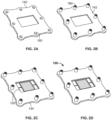
FIGS. 2A-D show an exemplary fabrication method of the subassembly ofFIG. 1 . -
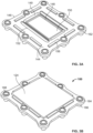
FIG. 3A is a perspective view of an underside of the stiffener with the installed hardware ofFIG. 1 . -
FIG. 3B is a perspective view of the underside of the subassembly ofFIG. 1 . -
FIG. 4A is a perspective view an exemplary chip. -
FIG. 4B is a perspective view the chip ofFIG. 4A shown bonded to an underside of a stiffener. -
FIG. 5 is a magnified photo of an exemplary aluminum silicon carbide ("AlSiC") composite showing silicon carbide particles in an aluminum matrix. -
FIG. 6 is a thermal comparison chart of particular materials in view of stiffener made of AlSiC. -
FIG. 7A is an assembled view of a mating assembly including a top plate secured to the subassembly ofFIG. 1 . -
FIG. 7B is an exploded perspective view of the mating assembly ofFIG. 7A . -
FIG. 7C is a side view of another exploded view of the mating assembly ofFIG. 7A . -
FIG. 7D is a cross-sectional view of the exploded side view ofFIG. 7C taken along a line A-A defining a mid-point of the shorter side surfaces of the top plate. -
FIG. 1 is a perspective view of apackage subassembly 100 of a semiconductor device including asubstrate 120 bonded to stiffener 140 with fasteners or threadedhardware 180 installed thereto. - The
stiffener 140 has a top surface, a bottom surface and an aperture through the top and bottom surfaces. The aperture may be generally central with respect to an outer perimeter of thestiffener 140, though in other examples the position of the aperture may be adjusted. For example, the size and shape and position of the aperture may be adapted based on circuitry of theunderlying substrate 120 to be exposed through the aperture. - The
substrate 120 may be coupled to the bottom surface of the stiffener, such as by an adhesive or other bonding techniques. A portion ofstiffener 140 may cover a portion of thesubstrate 120 when the substrate is coupled to the bottom surface of the stiffer. For example, the substrate may include circuitry on a least a first region on its top surface. The circuitry may include, by way of example only, microprocessors, memory, or other chips or components. When the substrate is assembled with the stiffener, the first region of the substrate including the circuitry may be accessible through the aperture of the stiffener. The portion of the substrate covered by the stiffener may be, for example, dead space or circuitry that does not need to be accessible. - According to some examples, described further below, the
stiffener 140 andsubstrate 120 may be included in an assembly, wherein a top plate is coupled to the top surface of the stiffener and an O-ring provides a seal between the stiffener and top plate. -
FIGS. 2A-D show an example assembly method ofsubassembly 100. InFIG. 2A ,stiffener 140 is sintered together. The stiffener may be formed of silicon carbide particles in an aluminum matrix, as one example. Post processing is completed, such as refining the peripheries of the stiffener, sanding the top or bottom surfaces thereof or ensuring holes and apertures meet specifications. InFIG. 2B , threadedhardware 180 is installed to atop surface 142 ofstiffener 140. InFIG. 2C , a substrate and/or chip is bonded to a bottom surface orunderside 144 ofstiffener 140. InFIG. 2D ,subassembly 100 is sputter coated before being soldered to a motherboard. WhileFIGS. 2A-2D provide one example, it should be understood that variations may be made. For example, coupling techniques other than bonding may be used, different coating techniques may be used, etc. For example, the stiffener could be coated or plated with different metals or polymers for adhesion improvement. In further examples, the stiffener could be made to be compatible for using a solder based or polymer adhesive based bonding. -
FIG. 3A is a perspective view of anunderside 144 ofstiffener 140. Theunderside 144 of thestiffener 140 may have at least one groove for receiving at least one protrusion extending from a chip and/or substrate. For example, first and second grooves in the stiffener may be configured to receive respective first and second protrusions of the substrate. - According to one example, the protrusions extending from the
underside 144 may each lie parallel to an edge of the central aperture of the stiffener. When the substrate is coupled to the bottom surface of the stiffener each of the plurality of protrusions may lie adjacent to a respective outer side surface of the substrate. In one example, the stiffener may have four protrusions in which each protrusion is configured to lie adjacent a respective outer surface side of a rectangular chip on the substrate when the substrate is coupled to the bottom surface of the stiffener. In other examples, additional or fewer protrusions may be included. -
Stiffener 140 has an irregularly shaped outer periphery orperimeter 146. Theaperture 150 defines an inner periphery orperimeter 148.Aperture 150 extends through top andbottom surfaces stiffener 140.Bottom surface 144 of stiffener may include at least onegroove 152 therein. -
FIG. 3A shows astiffener 140 with two recesses orgrooves 152 adjacent the longer sides ofinner periphery 148. Aramp surface 149 extending frombottom surface 144 towardtop surface 142 ofstiffener 140 is also provided. Ramp surfaces 149 are adjacent each of the shorter sides ofinner periphery 148.Protrusions 156 extending outwardly frombottom surface 144 ofstiffener 140 are also provided. Twoprotrusions 156 are shown forming a pair ofprotrusions 156 on each side ofstiffener 140 for a total of eightprotrusions 156 extending outwardly from a bottom surface ofstiffener 140.Stiffener 140 also includesperipheral apertures 160 extending through the top andbottom surfaces FIG. 2A ,stiffener 140 includes eightperipheral apertures 160. This is just one example of the number of recesses orgrooves 152,protrusions 156 andperipheral apertures 160 that stiffener 140 may have. In other examples,stiffener 140 may have more or less than two recesses orgrooves 152, more or less than twoprotrusions 156 and more or less than eightperipheral apertures 160. - Irregularly shaped
outer periphery 146 ofstiffener 140 may provide for weight optimization. Instead of a rectangular outer periphery,stiffener 140 is designed with aperipheral curve 162 about eachperipheral aperture 160. Each curve on a side surface of the stiffener may be approximately 180° while each curve on a corner of the stiffener may be approximately 270°. The lead line ofelement 162 shown inFIG. 3A is to a corner of theouter periphery 146 ofstiffener 140 while the curves adjacent this corner are on the aforementioned sides surfaces ofstiffener 140. The empty space between eachadjacent curves 162 reduces the weight of the stiffener while still providing the structural area needed to control warpage. -
Hardware 180 is installed through each ofperipheral apertures 160 ofstiffener 140. Each fastener orhardware 180 has abase 184, ashaft 186 and a threadedhole 188. To couple eachhardware 180 tostiffener 140,shaft 186 is inserted throughhole 188 from thebottom surface 144 and though thetop surface 142 ofstiffener 140 until based 184 come into directed contact withbottom surface 144. According to some examples, each fastener aperture or hole in the stiffener corresponds to a respective aperture or hole in the top plate. For example, each of the plurality of holes in the stiffener forms a pair with a respective one of the plurality of holes in the top plate. Each pair of the plurality of holes is adapted to receive a portion of a fastener therethrough for coupling the top plate to the stiffener. -
Hardware 180 may be utilized that can attach to a microprocessor such that it can handle the pressure loads under a direct liquid cooling regime while still being light enough to be soldered to a motherboard and handled in a high volume production environment. For example, a manifold may be configured to lie within an enclosure formed by the substrate, stiffener and top plate. The manifold may be configured to supply cooled liquid to the substrate. A portion of the manifold may lie within the central aperture of the stiffener in direct contact with the substrate when the manifold is within the enclosure formed by the substrate, stiffener and top plate. - As shown in
FIGS. 3B and4B , asubstrate 120 is coupled to abottom surface 144 ofstiffener 140.Subassembly 100 includes asubstrate 120 which also includes adie 130 which may also be referred to as a chip. Thedie 130 may be an integrated circuit ("IC") chip, system on chip ("SoC"), or portion thereof, that may include various passive and active microelectronic devices such as resistors, capacitors, inductors, diodes, metal-oxide semiconductor field effect ("MOSFET") transistors, CMOS transistors, bipolar junction transistors ("BJTs"), laterally diffused metal-oxide-silicon ("LDMOS") transistors, high power MOS transistors, other types of transistors, or other types of devices. Thedie 130 may comprise a memory device, a logic device, or other types of circuits, as examples.Die 130 is shown bonded to a carrier substrate orsubstrate 120.Substrate 120 can be, for example, a silicon substrate, a plastic substrate, a flexible substrate having polyimide and copper layers for example, a laminate substrate, a ceramic substrate, an interposer, or any other suitable support structure. -
Substrate 120 includes atop surface 122, abottom surface 124 andside surfaces 126 extending between top andbottom surfaces Top surface 122 also includes aramp surface 128 extending outwardly thereof that forms a perimeter ofchip 130. Adjacent the longer sides ofchip 130 areprotrusions 132 that also extending outwardly fromtop surface 122 ofsubstrate 120. - Prior to bonding
top surface 122 ofsubstrate 120 tobottom surface 144 of stiffener, a layer of adhesive 170 may be applied to the top surface ofsubstrate 120 and/or thebottom surface 144 ofstiffener 140. As an example,FIG. 4A shows adhesive 170 applied totop surface 122 ofsubstrate 120. The adhesive is used to mechanically couple togethersubstrate 120 andstiffener 140. Any type of adhesive used in the industry including but not limited to natural adhesive, synthetic adhesive, drying adhesives, thermoplastic adhesives, reactive adhesives, pressure sensitive adhesives, or any other commonly used adhesive may be used. - When positioning
substrate 120 with respect tostiffener 140 prior to bonding of these components,protrusions 132 of substrate are positioned withingrooves 152 ofstiffener 140 andside surfaces 126 ofsubstrate 120 are positionedadjacent protrusions 132 ofstiffener 140 as shown inFIG. 3B and4B .Ramp surface 128 ofsubstrate 120 is also positioned in contact with corresponding ramp surfaces 149 ofstiffener 140. -
FIG. 4B provides a transparency ofsubstrate 120 bonded tostiffener 140 which showscentral aperture 150 of stiffener even though atleast chip 130 ofsubstrate 120 is coveringcentral aperture 150 whensubstrate 120 is bonded tostiffener 140. - Subassembly 100 may be design according to particular specifications. For example, the weight of
subassembly 100 should be less than 130g total so that the ball grid array ("BGA") is not crushed during solder reflow. In one example, the optimized weight ofstiffener 140 plus hardware or rivetnuts 180 is less than 50g. With thechip 130 onsubstrate 120 or printed circuit board (PCB) being less than 25g and the adhesive weight used to bond thesubstrate 120 andchip 130 to stiffener 140 being less than 5g, the total package weight ofsubassembly 100 is approximately 80g, which is well under the maximum 130g weight specification for the total package. In other examples,stiffener 140 plushardware 180 may be more or less than 50g, thechip 130 onsubstrate 120 may be more or less than 25g and the adhesive used tobond stiffener 140 tosubstrate 120 may be more or less than 5g. - In designing the components of
subassembly 100, the total thermal mass should be low and conductivity should be high such that heat can be applied from above to melt the solder underneath without damaging other components. The outer periphery ofsubassembly 100 may be design to fit on an existing tray. Adhesive and O-ring joints/surfaces should provide sealing forsubassembly 100 for liquid water. The design ofsubassembly 100 should not promote any galvanic corrosion between electrolytically connected components. Thermal expansion ofsubassembly 100 should closely match the coefficient of a substrate it is bonded to for the purpose of minimizing thermal stresses. - According to some examples, the
stiffener 140 may be made of AlSiC. Threadedhardware 180 may be attached after the AlSiC is fabricated. AlSiC is a metal-ceramic composite material consisting of silicon carbide particles (SiC) dispersed in a matrix of aluminum alloy (A) as shown, for example, inFIG. 5 . The aluminum matrix contains high amount of dislocations, responsible for the strength of the material. The dislocations may be introduced during cooling by the SiC particles, due to their different thermal expansion coefficient. - AlSiC combines the benefits of high thermal conductivity (180-200 W/m K) of metal and low CTE of ceramic. With its composite features, AlSiC is an advanced packaging material for high technology thermal management. Its thermal expansion can be adjusted to match other materials, for example, silicon and gallium arsenide chips and various ceramics. When used in microelectronics as a substrate for power semiconductor devices and high density multi-chip modules, it aids with removal of waste heat.
-
FIG. 6 is a thermal comparison chart of particular materials in view ofstiffener 140 made of AlSiC. As can be seen, AlSiC has a coefficient of thermal expansion that is at least half that of planar circuit boards (in plane), 304 Stainless Steel and copper, for example. AlSiC has a thermal conductivity less than half of that of copper, but a much higher thermal conductivity than a circuit board or 304 Stainless Steel. The strain at +50 degrees C and relative strain as a function of percentage are highlighted between these materials as well. -
FIG. 2A discussed above states that stiffener 140 is sintered together. AlSiC parts may also be manufactured by near net shape approach, by creating a SiC preform by metal injection molding of an SiC-binder slurry, fired to remove the binder, and then infiltrated under pressure with molten aluminum. Parts can be made with sufficiently low tolerances to not require further machining. According to other examples, further processing ofstiffener 140 may be performed to meet certain specifications. - AlSiC is fully dense, without voids, and is hermetic. AlSiC can be plated with nickel and nickel-gold or by other metals by thermal spraying. Ceramic and metal insets can be inserted into the preform before aluminum infiltration, resulting in a hermetic seal. AlSiC can be also prepared by mechanical alloying. When lower degree of SiC content is used, parts can be stamped from AlSiC sheets.
-
FIG. 7A is an assembled view of amating assembly 300 whileFIG. 7B is an exploded view themating assembly 300 showing each of the components thereof.Mating assembly 300 includes the components ofsubassembly 100, namelysubstrate 120 andchip 130,stiffener 140, adhesive 170 andhardware 180 as well as the additional components of an O-ring 190, manifold 200,top plate 220 andfasteners 280. - Each fastener aperture or
hole 160 instiffener 140 corresponds to a respective aperture or hole 260 intop plate 220. For example, each of the plurality ofholes 160 instiffener 140 form a pair with a respective one of the plurality of holes 260 in thetop plate 220. Each pair of the plurality of holes 260 are adapted to receive a portion of afastener 280 therethrough for engaging threadedhardware 180 and couplingtop plate 220 to stiffener 140 as shown inFIG. 7A . -
Top plate 220 hastop portion 222 as shown inFIG. 7A and abottom portion 224 that can at least be partially be seen in the cross-sectional view ofFIG. 7D . There is an arrow inFIG. 4A pointing towardtop portion 222, which represents a flow regime or channels that would extend through thetop portion 222 andbottom portion 224 that are not shown with respect totop plate 220. Agroove 230 is formed inbottom portion 224 oftop plate 220.Groove 230 is configured to retain O-ring 190 whentop plate 220 is coupled tostiffener 140. In an exploded side view ofmating assembly 300 as shown inFIG. 7C , and as shown in the corresponding cross-sectional view ofFIG. 7D , the position of O-ring 190 with respect tocentral aperture 150 and its general orientation onstiffener 140 can be seen. -
FIG. 7D also shows an exploded view of the enclosure that manifold 200 is configured to lie within. The enclosure is formed whensubstrate 120,stiffener 140 andtop plate 220 are coupled together as shown inFIG. 7A .Manifold 200 is designed to direct flow over a microprocessor in order to significantly improve heat transfer between the microprocessor and the working fluid. A portion ofmanifold 200 is designed to lie withincentral aperture 150 ofstiffener 140 and is in direct contact withchip 130 ofsubstrate 120 when manifold 200 is within the enclosure formed bysubstrate 120,stiffener 140 andtop plate 220.Manifold 200 sits on top ofchip 130 with flow channels. It is designed with an intricate crossflow path for the coolant resulting in the improved crossflow path betweenchip 130 and the working fluid. Cooled fluid or liquid runs through aninlet channel 205 inmanifold 200 and on tochip 130. Liquid that has previously been used tocool chip 130 is expelled throughoutlet channels 215. - When
mating assembly 300 is fully assembled as shown inFIG. 7A , weight optimizedstiffener 140 may provide sealing ontop surface 142 thereof through the use of O-ring 190 and onbottom surface 144 thereof through the use ofadhesive 170. The top plate has a groove in an inner surface thereof that is configured to retain the O-ring when the top plate is coupled to the stiffener. -
Stiffener 140 provides warpage control for a lidless package while enabling direct liquid cooling ofchip 130 and/orsubstrate 120. Stiffener comprises weight optimization material such as AlSiC and geometry features such as irregularly shapedouter periphery 146. The weight optimization ofstiffener 140 reduces its thermal mass and the impact of weight concentrations during attachment ofstiffener 140, for example, to a motherboard. - Another aspect of the present disclosure relates to a weight optimized stiffener for use in a semiconductor device. In one example, the stiffener is made of AlSiC for its weight and thermal properties. An O-ring provides sealing between a top surface of the stiffener and a component of the semiconductor device and adhesive provides sealing between a bottom surface of the stiffener and another component of the semiconductor device. The stiffener provides warpage control for a lidless package while enabling direct liquid cooling of a chip or substrate.
- Further examples of the present disclosure are given below.
- Example 1. A device, comprising:
- a weight optimized stiffener having a top surface, a bottom surface, an irregularly shaped outer periphery and an inner periphery forming an aperture through the top and bottom surfaces,
- wherein the aperture is adapted to receive a portion of a substrate coupled to the bottom surface of the stiffener by an adhesive.
- Example 2. The device of example 1, wherein the stiffener is formed of silicon carbide particles in an aluminum matrix.
- Example 3. The device of example 1 or 2, further comprising:
a substrate coupled to the bottom surface of the stiffener by an adhesive, a portion of the substrate protruding into the aperture of the stiffener. - Example 4. The device of example 3, wherein the bottom surface of the stiffener has at least one recess for receiving at least one protrusion on the substrate, or
wherein the bottom surface of the stiffener has a plurality of protrusions extending therefrom that lie adjacent to outer side surfaces of the substrate when the substrate is coupled to the bottom surface of the stiffener. - Example 5. The device of example 3 or 4, further comprising:
- a top plate coupled to the top surface of the stiffener; and
- an O-ring for providing a seal between the stiffener and the top plate, and
- wherein optionally the stiffener has a plurality of holes corresponding to a plurality of holes in the top plate, each of the plurality of holes in the stiffener forming a pair with a respective one of the plurality of holes in the top plate, each pair of the plurality of holes adapted to receive a portion of a fastener therethrough for coupling the top plate to the stiffener.
- Example 6. The device of example 5, further comprising:
- a manifold configured to lie within an enclosure formed by the substrate, stiffener and top plate, the manifold configured to direct cooled liquid to the substrate, and
- wherein optionally a portion of the manifold lies within the aperture of the stiffener and is in direct contact with the substrate when the manifold is within the enclosure formed by the substrate, stiffener and top plate.
- Example 7. The device of example 5 or 6, wherein the top plate has a groove in an inner surface thereof that is configured to retain the O-ring when the top plate is coupled to the stiffener.
- Example 8. An assembly, comprising:
- a weight optimized stiffener having a top surface, a bottom surface, an outer periphery and an inner periphery forming an aperture through the top and bottom surfaces; and
- a substrate coupled to the bottom surface of the stiffener by an adhesive, a portion of the substrate protruding into the aperture of the stiffener.
- Example 9. The assembly of example 8, wherein the stiffener is formed of silicon carbide particles in an aluminum matrix.
- Example 10. The assembly of example 8 or 9, wherein the bottom surface of the stiffener has at least one recess for receiving at least one protrusion on the substrate, or
wherein the bottom surface of the stiffener has a plurality of protrusions extending therefrom that lie adjacent to outer side surfaces of the substrate when the substrate is coupled to the bottom surface of the stiffener. - Example 11. The assembly of example 9 or 10, further comprising:
- a top plate coupled to the top surface of the stiffener; and
- an O-ring for providing a seal between the stiffener and the top plate, and
- wherein optionally the stiffener has a plurality of holes corresponding to a plurality of holes in the top plate, each of the plurality of holes in the stiffener forming a pair with a respective one of the plurality of holes in the top plate, each pair of the plurality of holes adapted to receive a portion of a fastener therethrough for coupling the top plate to the stiffener.
- Example 12. The assembly of example 11, further comprising:
a manifold configured to lie within an enclosure formed by the substrate, stiffener and top plate, the manifold configured to direct cooled liquid to the substrate. - Example 13. The assembly of example 12, wherein a portion of the manifold lies within the central aperture of the stiffener and a bottom surface of the manifold is in direct contact with the substrate when the manifold is within the enclosure formed by the substrate, stiffener and top plate.
- Example 14. The assembly of any one of examples 11 to 13, wherein the top plate has a groove in an inner surface thereof that is configured to retain the O-ring when the top plate is coupled to the stiffener.
- Example 15. A method of assembling a semiconductor device for providing warpage control to a direct liquid cooled module, comprising:
- providing a weight optimized stiffener having a top surface, a bottom surface, an outer periphery and an inner periphery forming a central aperture through the top and bottom surfaces;
- providing a substrate having a top surface including circuitry on at least a first region of the top surface; and
- coupling the top surface of the substrate to the bottom surface of the stiffener such that the first region of the top surface of the substrate is accessible through the aperture of the stiffener.
- Unless otherwise stated, the foregoing alternative examples are not mutually exclusive, but may be implemented in various combinations to achieve unique advantages. As these and other variations and combinations of the features discussed above can be utilized without departing from the subject matter defined by the claims, the foregoing description should be taken by way of illustration rather than by way of limitation of the subject matter defined by the claims. In addition, the provision of the examples described herein, as well as clauses phrased as "such as," "including" and the like, should not be interpreted as limiting the subject matter of the claims to the specific examples; rather, the examples are intended to illustrate only one of many possible implementations. Further, the same reference numbers in different drawings can identify the same or similar elements.
Claims (12)
- A method of assembling a semiconductor device for providing warpage control to a direct liquid cooled module, comprising:providing a weight optimized stiffener having a top surface, a bottom surface, an outer periphery and an inner periphery forming a central aperture through the top and bottom surfaces;providing a substrate having a top surface including circuitry on at least a first region of the top surface; andcoupling the top surface of the substrate to the bottom surface of the stiffener such that the first region of the top surface of the substrate is accessible through the aperture of the stiffener,wherein a top plate is coupled to the top surface of the stiffener, anda manifold is configured to lie within an enclosure formed by the substrate, the stiffener and the top plate, the manifold configured to direct cooled liquid to the substrate,wherein the coupling the top surface of the substrate to the bottom surface comprises coupling the top surface to the bottom surface of the stiffener by an adhesive such that a portion of the substrate protrudes into the aperture of the stiffener.
- The method of claim 1, further comprising forming the stiffener of silicon carbide particles in an aluminum matrix.
- The method of claim 1 or 2, further comprising providing at least one recess in the bottom surface of the stiffener for receiving at least one protrusion on the substrate.
- The method of any one of claims 1 to 3, further comprising coupling a top plate to the top surface of the stiffener.
- The method of claim 4, further comprising providing a seal between the stiffener and the top plate.
- The method of claim 5, wherein the seal is provided by arranging an O-ring between the stiffener and the top plate.
- The method of claim 6, further comprising forming a groove in an inner surface of the top plate for receiving the O-ring.
- The method of claim 4, further comprising providing a manifold configured to lie within an enclosure formed by the substrate, the stiffener and the top plate, the manifold configured to direct cooled liquid to the substrate.
- The method of claim 8, wherein a portion of the manifold lies within the aperture of the stiffener and is in direct contact with the substrate when the manifold is within the enclosure formed by the substrate, the stiffener and the top plate.
- The method of any one of the preceding claims, further comprising:providing a plurality of holes in the top plate; andproviding a plurality of holes in the stiffener corresponding to the plurality of holes in the top plate;wherein each of the plurality of holes in the stiffener forms a pair with a respective one of the plurality of holes in the top plate.
- The method of claim 10, further comprising inserting at least a portion of a fastener in at least one pair of the plurality of holes for coupling the top plate to the stiffener.
- The method of any one of the preceding claims, wherein the outer periphery is irregularly shaped.
Applications Claiming Priority (2)
| Application Number | Priority Date | Filing Date | Title |
|---|---|---|---|
| US16/877,730 US11721641B2 (en) | 2020-05-19 | 2020-05-19 | Weight optimized stiffener and sealing structure for direct liquid cooled modules |
| EP20211008.6A EP3913663B1 (en) | 2020-05-19 | 2020-12-01 | Weight optimized stiffener and sealing structure for direct liquid cooled modules |
Related Parent Applications (2)
| Application Number | Title | Priority Date | Filing Date |
|---|---|---|---|
| EP20211008.6A Division EP3913663B1 (en) | 2020-05-19 | 2020-12-01 | Weight optimized stiffener and sealing structure for direct liquid cooled modules |
| EP20211008.6A Division-Into EP3913663B1 (en) | 2020-05-19 | 2020-12-01 | Weight optimized stiffener and sealing structure for direct liquid cooled modules |
Publications (3)
| Publication Number | Publication Date |
|---|---|
| EP4398297A2 true EP4398297A2 (en) | 2024-07-10 |
| EP4398297A3 EP4398297A3 (en) | 2024-10-30 |
| EP4398297B1 EP4398297B1 (en) | 2026-04-01 |
Family
ID=73698521
Family Applications (2)
| Application Number | Title | Priority Date | Filing Date |
|---|---|---|---|
| EP24178032.9A Active EP4398297B1 (en) | 2020-05-19 | 2020-12-01 | Weight optimized stiffener and sealing structure for direct liquid cooled modules |
| EP20211008.6A Active EP3913663B1 (en) | 2020-05-19 | 2020-12-01 | Weight optimized stiffener and sealing structure for direct liquid cooled modules |
Family Applications After (1)
| Application Number | Title | Priority Date | Filing Date |
|---|---|---|---|
| EP20211008.6A Active EP3913663B1 (en) | 2020-05-19 | 2020-12-01 | Weight optimized stiffener and sealing structure for direct liquid cooled modules |
Country Status (6)
| Country | Link |
|---|---|
| US (2) | US11721641B2 (en) |
| EP (2) | EP4398297B1 (en) |
| CN (2) | CN112185906B (en) |
| DK (1) | DK3913663T3 (en) |
| FI (1) | FI3913663T3 (en) |
| TW (2) | TWI829965B (en) |
Family Cites Families (30)
| Publication number | Priority date | Publication date | Assignee | Title |
|---|---|---|---|---|
| US5269372A (en) * | 1992-12-21 | 1993-12-14 | International Business Machines Corporation | Intersecting flow network for a cold plate cooling system |
| US5557503A (en) | 1995-05-12 | 1996-09-17 | International Business Machines Corporation | Circuit card having a large module strain relief and heat sink support |
| US5778523A (en) | 1996-11-08 | 1998-07-14 | W. L. Gore & Associates, Inc. | Method for controlling warp of electronic assemblies by use of package stiffener |
| US6011304A (en) * | 1997-05-05 | 2000-01-04 | Lsi Logic Corporation | Stiffener ring attachment with holes and removable snap-in heat sink or heat spreader/lid |
| US6315605B1 (en) | 2000-05-09 | 2001-11-13 | Fci Americas Technology, Inc. | Printed circuit board stiffener assembly |
| US8464781B2 (en) | 2002-11-01 | 2013-06-18 | Cooligy Inc. | Cooling systems incorporating heat exchangers and thermoelectric layers |
| US7516776B2 (en) | 2005-05-19 | 2009-04-14 | International Business Machines Corporation | Microjet module assembly |
| US7459782B1 (en) | 2005-10-05 | 2008-12-02 | Altera Corporation | Stiffener for flip chip BGA package |
| US7511957B2 (en) * | 2006-05-25 | 2009-03-31 | International Business Machines Corporation | Methods for fabricating a cooled electronic module employing a thermally conductive return manifold structure sealed to the periphery of a surface to be cooled |
| US20080054490A1 (en) | 2006-08-31 | 2008-03-06 | Ati Technologies Inc. | Flip-Chip Ball Grid Array Strip and Package |
| US7608924B2 (en) * | 2007-05-03 | 2009-10-27 | Delphi Technologies, Inc. | Liquid cooled power electronic circuit comprising stacked direct die cooled packages |
| US20080284047A1 (en) | 2007-05-15 | 2008-11-20 | Eric Tosaya | Chip Package with Stiffener Ring |
| WO2010087825A1 (en) | 2009-01-29 | 2010-08-05 | Hewlett-Packard Development Company, L.P. | Cooling apparatus |
| US9496199B2 (en) * | 2012-12-04 | 2016-11-15 | General Electric Company | Heat spreader with flexible tolerance mechanism |
| US9224673B2 (en) * | 2013-03-08 | 2015-12-29 | Taiwan Semiconductor Manufacturing Company, Ltd. | Packages for semiconductor devices, packaged semiconductor devices, and methods of cooling packaged semiconductor devices |
| US9265176B2 (en) * | 2013-03-08 | 2016-02-16 | International Business Machines Corporation | Multi-component electronic module with integral coolant-cooling |
| US9345169B1 (en) * | 2014-11-18 | 2016-05-17 | International Business Machines Corporation | Liquid-cooled heat sink assemblies |
| US9865522B2 (en) * | 2014-11-18 | 2018-01-09 | International Business Machines Corporation | Composite heat sink structures |
| US10090173B2 (en) | 2015-06-05 | 2018-10-02 | International Business Machines Corporation | Method of fabricating a chip module with stiffening frame and directional heat spreader |
| US10653332B2 (en) | 2015-07-17 | 2020-05-19 | Mc10, Inc. | Conductive stiffener, method of making a conductive stiffener, and conductive adhesive and encapsulation layers |
| US9583408B1 (en) * | 2015-08-21 | 2017-02-28 | International Business Machines Corporation | Reducing directional stress in an orthotropic encapsulation member of an electronic package |
| US10043730B2 (en) * | 2015-09-28 | 2018-08-07 | Xilinx, Inc. | Stacked silicon package assembly having an enhanced lid |
| WO2017119937A1 (en) * | 2016-01-07 | 2017-07-13 | Xilinx, Inc. | Stacked silicon package assembly having enhanced stiffener |
| US10643913B2 (en) * | 2017-12-06 | 2020-05-05 | Google Llc | Apparatus and mechanisms for reducing warpage and increasing surface mount technology yields in high performance integrated circuit packages |
| US10083920B1 (en) | 2018-02-01 | 2018-09-25 | Google Llc | Package stiffener for protecting semiconductor die |
| JP6493612B1 (en) | 2018-08-13 | 2019-04-03 | 富士電機株式会社 | Power semiconductor module and vehicle |
| US10561040B1 (en) | 2018-10-08 | 2020-02-11 | Hewlett Packard Enterprise Development Lp | Flexible gasket seal for direct liquid cooling of electronic devices |
| JP7098574B2 (en) * | 2019-05-28 | 2022-07-11 | 矢崎総業株式会社 | Heat dissipation structure |
| US11367628B2 (en) * | 2019-07-16 | 2022-06-21 | Advanced Micro Devices, Inc. | Molded chip package with anchor structures |
| US11282765B2 (en) * | 2020-03-11 | 2022-03-22 | Mellanox Technologies, Ltd. | Stiffener ring |
-
2020
- 2020-05-19 US US16/877,730 patent/US11721641B2/en active Active
- 2020-09-17 TW TW109132017A patent/TWI829965B/en active
- 2020-09-17 TW TW112150067A patent/TWI869132B/en active
- 2020-09-30 CN CN202011067664.1A patent/CN112185906B/en active Active
- 2020-09-30 CN CN202410515594.3A patent/CN118431090A/en active Pending
- 2020-12-01 EP EP24178032.9A patent/EP4398297B1/en active Active
- 2020-12-01 FI FIEP20211008.6T patent/FI3913663T3/en active
- 2020-12-01 EP EP20211008.6A patent/EP3913663B1/en active Active
- 2020-12-01 DK DK20211008.6T patent/DK3913663T3/en active
-
2023
- 2023-04-25 US US18/139,025 patent/US12588510B2/en active Active
Also Published As
| Publication number | Publication date |
|---|---|
| EP4398297A3 (en) | 2024-10-30 |
| EP3913663A1 (en) | 2021-11-24 |
| TWI869132B (en) | 2025-01-01 |
| US11721641B2 (en) | 2023-08-08 |
| US20210366841A1 (en) | 2021-11-25 |
| EP3913663B1 (en) | 2024-07-03 |
| US20230260931A1 (en) | 2023-08-17 |
| TWI829965B (en) | 2024-01-21 |
| FI3913663T3 (en) | 2024-08-27 |
| CN112185906B (en) | 2024-05-17 |
| CN118431090A (en) | 2024-08-02 |
| TW202418916A (en) | 2024-05-01 |
| US12588510B2 (en) | 2026-03-24 |
| DK3913663T3 (en) | 2024-09-30 |
| CN112185906A (en) | 2021-01-05 |
| TW202145859A (en) | 2021-12-01 |
| EP4398297B1 (en) | 2026-04-01 |
Similar Documents
| Publication | Publication Date | Title |
|---|---|---|
| TWI773566B (en) | Semiconductor package and printed circuit board assembly | |
| US12183659B2 (en) | Embedded cooling assemblies for advanced device packaging and methods of manufacturing the same | |
| US7119433B2 (en) | Packaging for enhanced thermal and structural performance of electronic chip modules | |
| US6665187B1 (en) | Thermally enhanced lid for multichip modules | |
| US6175497B1 (en) | Thermal vias-provided cavity-down IC package structure | |
| US7808781B2 (en) | Apparatus and methods for high-performance liquid cooling of multiple chips with disparate cooling requirements | |
| US6462410B1 (en) | Integrated circuit component temperature gradient reducer | |
| US12272619B2 (en) | Direct liquid cooling with O-ring sealing | |
| US5623394A (en) | Apparatus for cooling of chips using a plurality of customized thermally conductive materials | |
| US7250675B2 (en) | Method and apparatus for forming stacked die and substrate structures for increased packing density | |
| US5838545A (en) | High performance, low cost multi-chip modle package | |
| JPH0758254A (en) | Multi-chip module and manufacturing method thereof | |
| US20060091509A1 (en) | Flip chip package including a non-planar heat spreader and method of making the same | |
| US20070284711A1 (en) | Methods and apparatus for thermal management in a multi-layer embedded chip structure | |
| US12278150B2 (en) | Semiconductor package with annular package lid structure | |
| US12588510B2 (en) | Weight optimized stiffener and sealing structure for direct liquid cooled modules | |
| HK40044576B (en) | Weight optimized stiffener and sealing structure for direct liquid cooled modules | |
| HK40044576A (en) | Weight optimized stiffener and sealing structure for direct liquid cooled modules | |
| US12512390B2 (en) | Semiconductor package with liquid flow-over segmented inset lid | |
| US20250343099A1 (en) | Hybrid Material Lid, Heat Sink, or Cold Plate for Semiconductor Packages |
Legal Events
| Date | Code | Title | Description |
|---|---|---|---|
| PUAI | Public reference made under article 153(3) epc to a published international application that has entered the european phase |
Free format text: ORIGINAL CODE: 0009012 |
|
| STAA | Information on the status of an ep patent application or granted ep patent |
Free format text: STATUS: THE APPLICATION HAS BEEN PUBLISHED |
|
| AC | Divisional application: reference to earlier application |
Ref document number: 3913663 Country of ref document: EP Kind code of ref document: P |
|
| AK | Designated contracting states |
Kind code of ref document: A2 Designated state(s): AL AT BE BG CH CY CZ DE DK EE ES FI FR GB GR HR HU IE IS IT LI LT LU LV MC MK MT NL NO PL PT RO RS SE SI SK SM TR |
|
| PUAL | Search report despatched |
Free format text: ORIGINAL CODE: 0009013 |
|
| AK | Designated contracting states |
Kind code of ref document: A3 Designated state(s): AL AT BE BG CH CY CZ DE DK EE ES FI FR GB GR HR HU IE IS IT LI LT LU LV MC MK MT NL NO PL PT RO RS SE SI SK SM TR |
|
| RIC1 | Information provided on ipc code assigned before grant |
Ipc: H01L 23/36 20060101ALI20240925BHEP Ipc: H01L 23/473 20060101ALI20240925BHEP Ipc: H01L 23/00 20060101ALI20240925BHEP Ipc: H05K 7/20 20060101ALI20240925BHEP Ipc: H01L 23/40 20060101ALI20240925BHEP Ipc: H01L 23/367 20060101ALI20240925BHEP Ipc: H01L 23/16 20060101ALI20240925BHEP Ipc: H01L 23/04 20060101ALI20240925BHEP Ipc: H01L 25/04 20230101AFI20240925BHEP |
|
| STAA | Information on the status of an ep patent application or granted ep patent |
Free format text: STATUS: REQUEST FOR EXAMINATION WAS MADE |
|
| 17P | Request for examination filed |
Effective date: 20250423 |
|
| GRAP | Despatch of communication of intention to grant a patent |
Free format text: ORIGINAL CODE: EPIDOSNIGR1 |
|
| STAA | Information on the status of an ep patent application or granted ep patent |
Free format text: STATUS: GRANT OF PATENT IS INTENDED |
|
| RIC1 | Information provided on ipc code assigned before grant |
Ipc: H01L 25/04 20230101AFI20250924BHEP Ipc: H01L 23/04 20060101ALI20250924BHEP Ipc: H01L 23/16 20060101ALI20250924BHEP Ipc: H01L 23/367 20060101ALI20250924BHEP Ipc: H01L 23/40 20060101ALI20250924BHEP Ipc: H05K 7/20 20060101ALI20250924BHEP Ipc: H01L 23/00 20060101ALI20250924BHEP Ipc: H01L 23/473 20060101ALI20250924BHEP Ipc: H01L 23/36 20060101ALI20250924BHEP |
|
| INTG | Intention to grant announced |
Effective date: 20251021 |
|
| GRAS | Grant fee paid |
Free format text: ORIGINAL CODE: EPIDOSNIGR3 |
|
| GRAA | (expected) grant |
Free format text: ORIGINAL CODE: 0009210 |
|
| STAA | Information on the status of an ep patent application or granted ep patent |
Free format text: STATUS: THE PATENT HAS BEEN GRANTED |
|
| AC | Divisional application: reference to earlier application |
Ref document number: 3913663 Country of ref document: EP Kind code of ref document: P |
|
| AK | Designated contracting states |
Kind code of ref document: B1 Designated state(s): AL AT BE BG CH CY CZ DE DK EE ES FI FR GB GR HR HU IE IS IT LI LT LU LV MC MK MT NL NO PL PT RO RS SE SI SK SM TR |
|
| P01 | Opt-out of the competence of the unified patent court (upc) registered |
Free format text: CASE NUMBER: UPC_APP_0006055_4398297/2026 Effective date: 20260219 |
|
| REG | Reference to a national code |
Ref country code: CH Ref legal event code: F10 Free format text: ST27 STATUS EVENT CODE: U-0-0-F10-F00 (AS PROVIDED BY THE NATIONAL OFFICE) Effective date: 20260401 Ref country code: GB Ref legal event code: FG4D |
|
| REG | Reference to a national code |
Ref country code: IE Ref legal event code: FG4D |
|
| REG | Reference to a national code |
Ref country code: DE Ref legal event code: R096 Ref document number: 602020069884 Country of ref document: DE |