EP4398039A1 - Apparatus for substrate processing - Google Patents
Apparatus for substrate processing Download PDFInfo
- Publication number
- EP4398039A1 EP4398039A1 EP23740004.9A EP23740004A EP4398039A1 EP 4398039 A1 EP4398039 A1 EP 4398039A1 EP 23740004 A EP23740004 A EP 23740004A EP 4398039 A1 EP4398039 A1 EP 4398039A1
- Authority
- EP
- European Patent Office
- Prior art keywords
- substrate
- speed
- mask
- exposure
- coating
- Prior art date
- Legal status (The legal status is an assumption and is not a legal conclusion. Google has not performed a legal analysis and makes no representation as to the accuracy of the status listed.)
- Pending
Links
Images


Classifications
-
- G—PHYSICS
- G03—PHOTOGRAPHY; CINEMATOGRAPHY; ANALOGOUS TECHNIQUES USING WAVES OTHER THAN OPTICAL WAVES; ELECTROGRAPHY; HOLOGRAPHY
- G03F—PHOTOMECHANICAL PRODUCTION OF TEXTURED OR PATTERNED SURFACES, e.g. FOR PRINTING, FOR PROCESSING OF SEMICONDUCTOR DEVICES; MATERIALS THEREFOR; ORIGINALS THEREFOR; APPARATUS SPECIALLY ADAPTED THEREFOR
- G03F7/00—Photomechanical, e.g. photolithographic, production of textured or patterned surfaces, e.g. printing surfaces; Materials therefor, e.g. comprising photoresists; Apparatus specially adapted therefor
- G03F7/16—Coating processes; Apparatus therefor
-
- G—PHYSICS
- G03—PHOTOGRAPHY; CINEMATOGRAPHY; ANALOGOUS TECHNIQUES USING WAVES OTHER THAN OPTICAL WAVES; ELECTROGRAPHY; HOLOGRAPHY
- G03F—PHOTOMECHANICAL PRODUCTION OF TEXTURED OR PATTERNED SURFACES, e.g. FOR PRINTING, FOR PROCESSING OF SEMICONDUCTOR DEVICES; MATERIALS THEREFOR; ORIGINALS THEREFOR; APPARATUS SPECIALLY ADAPTED THEREFOR
- G03F7/00—Photomechanical, e.g. photolithographic, production of textured or patterned surfaces, e.g. printing surfaces; Materials therefor, e.g. comprising photoresists; Apparatus specially adapted therefor
- G03F7/70—Microphotolithographic exposure; Apparatus therefor
- G03F7/708—Construction of apparatus, e.g. environment aspects, hygiene aspects or materials
- G03F7/70991—Connection with other apparatus, e.g. multiple exposure stations, particular arrangement of exposure apparatus and pre-exposure and/or post-exposure apparatus; Shared apparatus, e.g. having shared radiation source, shared mask or workpiece stage, shared base-plate; Utilities, e.g. cable, pipe or wireless arrangements for data, power, fluids or vacuum
-
- B—PERFORMING OPERATIONS; TRANSPORTING
- B08—CLEANING
- B08B—CLEANING IN GENERAL; PREVENTION OF FOULING IN GENERAL
- B08B3/00—Cleaning by methods involving the use or presence of liquid or steam
- B08B3/02—Cleaning by the force of jets or sprays
-
- C—CHEMISTRY; METALLURGY
- C25—ELECTROLYTIC OR ELECTROPHORETIC PROCESSES; APPARATUS THEREFOR
- C25F—PROCESSES FOR THE ELECTROLYTIC REMOVAL OF MATERIALS FROM OBJECTS; APPARATUS THEREFOR
- C25F3/00—Electrolytic etching or polishing
- C25F3/02—Etching
- C25F3/14—Etching locally
-
- G—PHYSICS
- G03—PHOTOGRAPHY; CINEMATOGRAPHY; ANALOGOUS TECHNIQUES USING WAVES OTHER THAN OPTICAL WAVES; ELECTROGRAPHY; HOLOGRAPHY
- G03F—PHOTOMECHANICAL PRODUCTION OF TEXTURED OR PATTERNED SURFACES, e.g. FOR PRINTING, FOR PROCESSING OF SEMICONDUCTOR DEVICES; MATERIALS THEREFOR; ORIGINALS THEREFOR; APPARATUS SPECIALLY ADAPTED THEREFOR
- G03F7/00—Photomechanical, e.g. photolithographic, production of textured or patterned surfaces, e.g. printing surfaces; Materials therefor, e.g. comprising photoresists; Apparatus specially adapted therefor
- G03F7/16—Coating processes; Apparatus therefor
- G03F7/162—Coating on a rotating support, e.g. using a whirler or a spinner
-
- G—PHYSICS
- G03—PHOTOGRAPHY; CINEMATOGRAPHY; ANALOGOUS TECHNIQUES USING WAVES OTHER THAN OPTICAL WAVES; ELECTROGRAPHY; HOLOGRAPHY
- G03F—PHOTOMECHANICAL PRODUCTION OF TEXTURED OR PATTERNED SURFACES, e.g. FOR PRINTING, FOR PROCESSING OF SEMICONDUCTOR DEVICES; MATERIALS THEREFOR; ORIGINALS THEREFOR; APPARATUS SPECIALLY ADAPTED THEREFOR
- G03F7/00—Photomechanical, e.g. photolithographic, production of textured or patterned surfaces, e.g. printing surfaces; Materials therefor, e.g. comprising photoresists; Apparatus specially adapted therefor
- G03F7/16—Coating processes; Apparatus therefor
- G03F7/168—Finishing the coated layer, e.g. drying, baking, soaking
-
- G—PHYSICS
- G03—PHOTOGRAPHY; CINEMATOGRAPHY; ANALOGOUS TECHNIQUES USING WAVES OTHER THAN OPTICAL WAVES; ELECTROGRAPHY; HOLOGRAPHY
- G03F—PHOTOMECHANICAL PRODUCTION OF TEXTURED OR PATTERNED SURFACES, e.g. FOR PRINTING, FOR PROCESSING OF SEMICONDUCTOR DEVICES; MATERIALS THEREFOR; ORIGINALS THEREFOR; APPARATUS SPECIALLY ADAPTED THEREFOR
- G03F7/00—Photomechanical, e.g. photolithographic, production of textured or patterned surfaces, e.g. printing surfaces; Materials therefor, e.g. comprising photoresists; Apparatus specially adapted therefor
- G03F7/20—Exposure; Apparatus therefor
-
- G—PHYSICS
- G03—PHOTOGRAPHY; CINEMATOGRAPHY; ANALOGOUS TECHNIQUES USING WAVES OTHER THAN OPTICAL WAVES; ELECTROGRAPHY; HOLOGRAPHY
- G03F—PHOTOMECHANICAL PRODUCTION OF TEXTURED OR PATTERNED SURFACES, e.g. FOR PRINTING, FOR PROCESSING OF SEMICONDUCTOR DEVICES; MATERIALS THEREFOR; ORIGINALS THEREFOR; APPARATUS SPECIALLY ADAPTED THEREFOR
- G03F7/00—Photomechanical, e.g. photolithographic, production of textured or patterned surfaces, e.g. printing surfaces; Materials therefor, e.g. comprising photoresists; Apparatus specially adapted therefor
- G03F7/20—Exposure; Apparatus therefor
- G03F7/2002—Exposure; Apparatus therefor with visible light or UV light, through an original having an opaque pattern on a transparent support, e.g. film printing, projection printing; by reflection of visible or UV light from an original such as a printed image
- G03F7/201—Exposure; Apparatus therefor with visible light or UV light, through an original having an opaque pattern on a transparent support, e.g. film printing, projection printing; by reflection of visible or UV light from an original such as a printed image characterised by an oblique exposure; characterised by the use of plural sources; characterised by the rotation of the optical device; characterised by a relative movement of the optical device, the light source, the sensitive system or the mask
-
- G—PHYSICS
- G03—PHOTOGRAPHY; CINEMATOGRAPHY; ANALOGOUS TECHNIQUES USING WAVES OTHER THAN OPTICAL WAVES; ELECTROGRAPHY; HOLOGRAPHY
- G03F—PHOTOMECHANICAL PRODUCTION OF TEXTURED OR PATTERNED SURFACES, e.g. FOR PRINTING, FOR PROCESSING OF SEMICONDUCTOR DEVICES; MATERIALS THEREFOR; ORIGINALS THEREFOR; APPARATUS SPECIALLY ADAPTED THEREFOR
- G03F7/00—Photomechanical, e.g. photolithographic, production of textured or patterned surfaces, e.g. printing surfaces; Materials therefor, e.g. comprising photoresists; Apparatus specially adapted therefor
- G03F7/20—Exposure; Apparatus therefor
- G03F7/2022—Multi-step exposure, e.g. hybrid; backside exposure; blanket exposure, e.g. for image reversal; edge exposure, e.g. for edge bead removal; corrective exposure
- G03F7/2032—Simultaneous exposure of the front side and the backside
-
- G—PHYSICS
- G03—PHOTOGRAPHY; CINEMATOGRAPHY; ANALOGOUS TECHNIQUES USING WAVES OTHER THAN OPTICAL WAVES; ELECTROGRAPHY; HOLOGRAPHY
- G03F—PHOTOMECHANICAL PRODUCTION OF TEXTURED OR PATTERNED SURFACES, e.g. FOR PRINTING, FOR PROCESSING OF SEMICONDUCTOR DEVICES; MATERIALS THEREFOR; ORIGINALS THEREFOR; APPARATUS SPECIALLY ADAPTED THEREFOR
- G03F7/00—Photomechanical, e.g. photolithographic, production of textured or patterned surfaces, e.g. printing surfaces; Materials therefor, e.g. comprising photoresists; Apparatus specially adapted therefor
- G03F7/20—Exposure; Apparatus therefor
- G03F7/2035—Exposure; Apparatus therefor simultaneous coating and exposure; using a belt mask, e.g. endless
-
- G—PHYSICS
- G03—PHOTOGRAPHY; CINEMATOGRAPHY; ANALOGOUS TECHNIQUES USING WAVES OTHER THAN OPTICAL WAVES; ELECTROGRAPHY; HOLOGRAPHY
- G03F—PHOTOMECHANICAL PRODUCTION OF TEXTURED OR PATTERNED SURFACES, e.g. FOR PRINTING, FOR PROCESSING OF SEMICONDUCTOR DEVICES; MATERIALS THEREFOR; ORIGINALS THEREFOR; APPARATUS SPECIALLY ADAPTED THEREFOR
- G03F7/00—Photomechanical, e.g. photolithographic, production of textured or patterned surfaces, e.g. printing surfaces; Materials therefor, e.g. comprising photoresists; Apparatus specially adapted therefor
- G03F7/26—Processing photosensitive materials; Apparatus therefor
- G03F7/42—Stripping or agents therefor
-
- G—PHYSICS
- G03—PHOTOGRAPHY; CINEMATOGRAPHY; ANALOGOUS TECHNIQUES USING WAVES OTHER THAN OPTICAL WAVES; ELECTROGRAPHY; HOLOGRAPHY
- G03F—PHOTOMECHANICAL PRODUCTION OF TEXTURED OR PATTERNED SURFACES, e.g. FOR PRINTING, FOR PROCESSING OF SEMICONDUCTOR DEVICES; MATERIALS THEREFOR; ORIGINALS THEREFOR; APPARATUS SPECIALLY ADAPTED THEREFOR
- G03F7/00—Photomechanical, e.g. photolithographic, production of textured or patterned surfaces, e.g. printing surfaces; Materials therefor, e.g. comprising photoresists; Apparatus specially adapted therefor
- G03F7/26—Processing photosensitive materials; Apparatus therefor
- G03F7/42—Stripping or agents therefor
- G03F7/422—Stripping or agents therefor using liquids only
-
- G—PHYSICS
- G03—PHOTOGRAPHY; CINEMATOGRAPHY; ANALOGOUS TECHNIQUES USING WAVES OTHER THAN OPTICAL WAVES; ELECTROGRAPHY; HOLOGRAPHY
- G03F—PHOTOMECHANICAL PRODUCTION OF TEXTURED OR PATTERNED SURFACES, e.g. FOR PRINTING, FOR PROCESSING OF SEMICONDUCTOR DEVICES; MATERIALS THEREFOR; ORIGINALS THEREFOR; APPARATUS SPECIALLY ADAPTED THEREFOR
- G03F7/00—Photomechanical, e.g. photolithographic, production of textured or patterned surfaces, e.g. printing surfaces; Materials therefor, e.g. comprising photoresists; Apparatus specially adapted therefor
- G03F7/70—Microphotolithographic exposure; Apparatus therefor
- G03F7/70425—Imaging strategies, e.g. for increasing throughput or resolution, printing product fields larger than the image field or compensating lithography- or non-lithography errors, e.g. proximity correction, mix-and-match, stitching or double patterning
- G03F7/70433—Layout for increasing efficiency or for compensating imaging errors, e.g. layout of exposure fields for reducing focus errors; Use of mask features for increasing efficiency or for compensating imaging errors
-
- G—PHYSICS
- G03—PHOTOGRAPHY; CINEMATOGRAPHY; ANALOGOUS TECHNIQUES USING WAVES OTHER THAN OPTICAL WAVES; ELECTROGRAPHY; HOLOGRAPHY
- G03F—PHOTOMECHANICAL PRODUCTION OF TEXTURED OR PATTERNED SURFACES, e.g. FOR PRINTING, FOR PROCESSING OF SEMICONDUCTOR DEVICES; MATERIALS THEREFOR; ORIGINALS THEREFOR; APPARATUS SPECIALLY ADAPTED THEREFOR
- G03F7/00—Photomechanical, e.g. photolithographic, production of textured or patterned surfaces, e.g. printing surfaces; Materials therefor, e.g. comprising photoresists; Apparatus specially adapted therefor
- G03F7/70—Microphotolithographic exposure; Apparatus therefor
- G03F7/70425—Imaging strategies, e.g. for increasing throughput or resolution, printing product fields larger than the image field or compensating lithography- or non-lithography errors, e.g. proximity correction, mix-and-match, stitching or double patterning
- G03F7/70466—Multiple exposures, e.g. combination of fine and coarse exposures, double patterning or multiple exposures for printing a single feature
-
- G—PHYSICS
- G03—PHOTOGRAPHY; CINEMATOGRAPHY; ANALOGOUS TECHNIQUES USING WAVES OTHER THAN OPTICAL WAVES; ELECTROGRAPHY; HOLOGRAPHY
- G03F—PHOTOMECHANICAL PRODUCTION OF TEXTURED OR PATTERNED SURFACES, e.g. FOR PRINTING, FOR PROCESSING OF SEMICONDUCTOR DEVICES; MATERIALS THEREFOR; ORIGINALS THEREFOR; APPARATUS SPECIALLY ADAPTED THEREFOR
- G03F7/00—Photomechanical, e.g. photolithographic, production of textured or patterned surfaces, e.g. printing surfaces; Materials therefor, e.g. comprising photoresists; Apparatus specially adapted therefor
- G03F7/70—Microphotolithographic exposure; Apparatus therefor
- G03F7/70691—Handling of masks or workpieces
- G03F7/707—Chucks, e.g. chucking or un-chucking operations or structural details
-
- B—PERFORMING OPERATIONS; TRANSPORTING
- B08—CLEANING
- B08B—CLEANING IN GENERAL; PREVENTION OF FOULING IN GENERAL
- B08B2203/00—Details of cleaning machines or methods involving the use or presence of liquid or steam
- B08B2203/02—Details of machines or methods for cleaning by the force of jets or sprays
-
- H—ELECTRICITY
- H01—ELECTRIC ELEMENTS
- H01M—PROCESSES OR MEANS, e.g. BATTERIES, FOR THE DIRECT CONVERSION OF CHEMICAL ENERGY INTO ELECTRICAL ENERGY
- H01M4/00—Electrodes
- H01M4/02—Electrodes composed of, or comprising, active material
- H01M4/64—Carriers or collectors
- H01M4/70—Carriers or collectors characterised by shape or form
Definitions
- the material cannot continuously move at a uniform speed in the exposure device, so that the exposure device cannot be integrate with the coating device, the drying device and other devices.
- multiple separate devices are required for the processing of the current collector, which results in high equipment cost and cannot save on the time cost of transferring the current collector between the multiple devices, thus limiting the processing efficiency of the current collector.
- the current collector is processed by multiple separate devices, which cannot achieve high consistency.
- FIG. 1 shows a schematic structural diagram of a vehicle 1 according to the present application.
- the vehicle 1 may be a fuel vehicle, a gas vehicle or a new-energy vehicle.
- the new-energy vehicle may be a battery electric vehicle, a hybrid vehicle, an extended-range vehicle, etc.
- a motor 11, a controller 12 and a battery 10 may be provided inside the vehicle 1.
- the controller 12 is configured to control the battery 10 to supply power to the motor 11.
- the battery 10 may be arranged at the bottom, the front or the rear of the vehicle 1.
- the battery 10 may be configured to supply power to the vehicle 1.
- the battery 10 may serve as an operating power supply for the vehicle 1 for use in a circuit system of the vehicle 1 to meet, for example, the operating power demand during the startup, navigation and traveling of the vehicle 1.
- the battery 10 may not only serve as an operation power supply for the vehicle 1, but may also serve as a driving power supply for the vehicle 1, in place of or partially in place of fuel or natural gas, to supply driving power to the vehicle 1.
- a drying device 302 is configured to receive the substrate 30, which is coated by means of the coating device 301, at the first speed and dry the material.
- An etching device304 is configured to receive the substrate 30, which is exposed by means of the exposure device 303, at the first speed and etch the material and a portion of the substrate 30 in an unexposed region of the substrate.
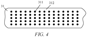
- FIG. 4 is a schematic structural diagram of a mask 31 according to an embodiment of the present application.
- the mask 31 has light-shielding portions 311 and a light-transmitting portion 312, and the light-shielding portions 311 and/or the light-transmitting portion 312 constitute an exposure pattern on the mask 31.
- the apparatus 300 further includes a feeding device 305 configured to convey the substrate 30 at the first speed in the feeding direction.
- the feeding device 305 in this embodiment of the present application is of, for example, but not limited to, a roll-to-roll structure.
- the feeding device 305 may also be in the form of a clamping and feeding mechanism having a manipulator, etc.
- the cleaning device 306 uses a combined structure of the spray rod 3061 and the cleaning tank 3062, and can quickly clean the etched substrate 30 to remove the residual material, etching liquid and other contaminants from the surface of the substrate 30, so that the apparatus 300 outputs the substrate 30 that can be directly used.
- the coating device 301 is also provided with a coating roller 3012.
- the coating roller 3012 is located between the two feeding rollers of the first feeding module 3011, and is configured to coat the substrate 30 in the vertical state with the material.
- the surface of the coating roller 3012 has a textured structure, the coating roller 3012 is partially immersed in a material tray, and during coating, the coating roller 3012 rotates to move the material such that the material passes through a flexible scraper and is then taken away by the reversely moving substrate 30 so as to coat the substrate 30 with a layer of material.
- the drying device 302 includes multiple heating tubes 3021 and multiple air knives 3022.
- the multiple heating tubes 3021 and multiple air knives 3022 are disposed at intervals on the two sides of the substrate 30 in the feeding direction.
- the arrangement of the multiple heating tubes 3021 and the multiple air knives 3022 at intervals means that, on each side of the substrate 30, the heating tubes 3021 and the air knives 3022 are spaced apart from each other, with one air knife 3022 being provided between two adjacent heating tubes 3021, and one heating tube 3021 being provided between two adjacent air knives 3022. It should be understood that, in some other embodiments, the number and arrangement of the heating tubes 3021 and the air knives 3022 can be configured according to the drying speed, feeding speed, etc. required for processing the substrate 30. For example, three heating tubes 3021 are provided between two adjacent air knives 3022.
- the material coated on the substrate 30 can be quickly dried for pre-curing of the material, and the substrate 30 does not need to stay in the drying device 302, so that the drying device 302 can cooperate with other devices to allow the substrate 30 to always travel at the same feeding speed in the feeding direction, which facilitates integration of the apparatus 300.
- the exposure device303 includes a mask conveying module 3031.
- the mask conveying module 3031 is configured to continuously convey the mask 31 at the first speed in the feeding direction.
- the exposure device 303 can perform continuous processing of a complex pattern, which improves the operation efficiency and performance of the exposure device 303 and is thus conducive to improving the efficiency and performance of the apparatus 300.
- the mask 31 is a strip-shaped mask
- the mask conveying module 3031 is configured to convey the strip-shaped mask to the exposure region at the first speed.
- the strip-shaped mask 31 may be conveyed in a roll-to-roll manner, so as to keep the mask 31 to move synchronously with the substrate 30 in the exposure region through a release and recovery process similar to that of the substrate 30. This will not be described herein again.
- the endless mask 31 is supported by the first drive roller 3031a and the driven roller 3031b provided on the inside to form a closed structure, and the first drive roller 3031a and the driven roller 3031b form a cyclic driving mechanism, so that the endless mask 31 can rotate in circles as the first drive roller 3031a and the driven roller 3031b rotate, and the endless mask 31 with the pattern can pass through the exposure region and then be rotated to the exposure region again.
- the mask conveying module 3031 rotates the mask 31 by means of the structure of the drive roller 3031a and the driven roller 3031b, and can control the movement conditions of the mask 31 by means of controlling the rotation speed and rotation direction of the drive roller 3031a and fix the movement path of the mask 31 by means of the driven roller 3031b, so as to achieve flexible control of the mask 31 to improve the flexibility of the exposure device 303, which is conducive to improving the treatment performance of the substrate treatment apparatus 300.
- the etching device 304 includes a conductive roller 3041, a first electrode 3042 and an etching tank 3043.
- the conductive roller 3041 and the first electrode 3042 are disposed in the etching tank 3043, and the etching tank 3043 holds an electrolyte solution.
- the conductive roller 3041 and the first electrode 3042 have opposite polarities, and the conductive roller 3041 comes into contact with the exposed substrate 30 and conveys the substrate 30 to the etching tank 3043 at the first speed.
- multiple first electrodes 3042 may be provided and disposed in the etching tank 3043 and close to the substrate 30.
- the conductive roller 3041 and the first electrode 3042 with opposite polarities form a cathode and an anode in a dielectric solution.
- the substrate 30 is a current collector, and the portions of the current collector that are not coated with photoresist will be etched so as to form a corresponding pattern or through hole.
- the electrochemical etching is taken as a specific example, but in some other embodiments, the etching device 304 may also use physical etching, dry etching, etc. to etch the substrate.
Landscapes
- Physics & Mathematics (AREA)
- General Physics & Mathematics (AREA)
- Engineering & Computer Science (AREA)
- Chemical & Material Sciences (AREA)
- Organic Chemistry (AREA)
- Electrochemistry (AREA)
- Materials Engineering (AREA)
- Metallurgy (AREA)
- Chemical Kinetics & Catalysis (AREA)
- Computer Networks & Wireless Communication (AREA)
- Health & Medical Sciences (AREA)
- Environmental & Geological Engineering (AREA)
- Epidemiology (AREA)
- Public Health (AREA)
- Manufacturing Of Printed Circuit Boards (AREA)
- Coating Apparatus (AREA)
Abstract
Description
- The present patent document claims for the priority and benefit of
Chinese patent application No. 202220092551.5, filed on January 14, 2022 - The present application relates to the field of substrate treatment, and in particular to a substrate treatment apparatus.
- With the rapid development of electronic products, higher requirements have been put forward for electronic processing. In an etching process, which is one of the important processes in electronic processing, a base or a material coated on the base is selectively removed by means of physical or chemical methods so as to design various fine structures on the base.
- In general, a substrate treatment process consists of coating, drying, exposure, developing and etching, which are respectively carried out by means of separate apparatuses such as a coater, a dryer and an exposure machine. These separate apparatuses cannot be integrated, and can neither control over the consistency of substrate treatment nor save on the time of transferring the substrate between the steps and the equipment cost, thus limiting the quality and efficiency of substrate treatment. Therefore, how to improve the substrate treatment efficiency is a problem to be solved.
- According to embodiments of the present application, there is provided a substrate treatment apparatus, by which the steps of coating, drying, exposure and etching for a substrate can be carried out by one apparatus, so that there is no need to transfer the substrate between the steps, thereby effectively improving the quality and efficiency of substrate treatment.
- In a first aspect, there is provided a substrate treatment apparatus, including: a coating device configured to coat a substrate, which is conveyed at a first speed in a feeding direction, with a material; a drying device configured to receive the substrate, which is coated by means of the coating device, at the first speed and dry the material; an exposure device configured to receive the substrate, which is dried by means of the drying device, at the first speed and continuously convey a mask at the first speed in the feeding direction, the mask being used for regional shading during exposure of the material by means of the exposure device, so that the material is subjected to continuous and regional exposure at the first speed by means of the exposure device; and an etching device configured to receive the substrate, which is exposed by means of the exposure device, at the first speed and etch the material and a portion of the substrate in an unexposed region of the substrate.
- In the embodiments of the present application, the exposure device can continuously convey the mask in the feeding direction, and during the exposure, the mask can move synchronously with the substrate in an exposure region, so that the substrate does not need to periodically stay in the exposure region. On this basis, the material can be conveyed to the devices at the same feeding speed and processed in the steps at the same feeding speed, and the exposure device, the coating device, the drying device and the etching device can be integrated into one apparatus to form an integrated apparatus, thereby saving on the time of transferring the substrate between the treatment steps during the substrate treatment process to improve the substrate treatment efficiency. In addition, the substrate treatment is implemented by means of the integrated apparatus, which is also conducive to saving on the equipment cost for transferring the substrate between the treatment steps.
- In some embodiments, the apparatus further includes: a feeding device configured to convey the substrate at the first speed in the feeding direction.
- In the embodiments of the present application, the substrate is continuously conveyed at the first speed by means of the feeding device, which facilitates controlling the movement conditions, such as the direction of movement and the speed of movement, of the substrate in the devices. This improves the consistency of movement of the substrate in the apparatus, and is conducive to improving the substrate treatment consistency and quality.
- In some embodiments, the apparatus further includes: a cleaning device configured to receive the substrate, which is etched by means of the etching device, at the first speed and clean the substrate.
- In the embodiments of the present application, the cleaning device can also be integrated in the substrate treatment apparatus to clean the etched substrate, so that the substrate output from the substrate treatment apparatus can be directly used, allowing the substrate treatment apparatus to have more functions and improving the performance of the substrate treatment apparatus.
- In some embodiments, the coating device includes: a first feeding module configured to allow the feeding direction in the coating device to be a vertical direction.
- In the embodiments of the present application, the coating device is provided with a first feeding module different from the feeding device, so that at least part of the substrate is in a vertical state in the coating device. The substrate is conveyed in the vertical direction in the coating device, which can make dust naturally fall off under gravity and reduce the dust attached to the material or the substrate, thereby improving the coating quality. In addition, the substrate is conveyed vertically during coating, so that the structure is compact, and the overall volume of the coating device can be reduced, thereby improving the space utilization of the substrate treatment apparatus.
- In some embodiments, the coating device performs coating by means of a gravure coating process.
- In the embodiments of the present application, by means of the gravure coating, the substrate can be uniformly and continuously coated with a thin layer of material, and the material has no defects such as adhesive residues and folds on the surface, which is conducive to improving the coating quality.
- In some embodiments, the substrate has a first surface and a second surface opposite to the first surface, and the coating device is configured to coat the first surface and the second surface with the material.
- In the embodiments of the present application, the coating device can coat the substrate on both sides at the same time, which improves the coating efficiency and is thus conducive to improving the substrate treatment efficiency.
- In some embodiments, the drying device includes: a plurality of heating tubes and a plurality of air knives arranged at intervals on two sides of the substrate in the feeding direction.
- In the embodiments of the present application, with the combination of the air knives and the heating tubes, the material coated on the substrate can be quickly dried for pre-curing of the material, and the substrate does not need to stay in the drying device, so that the drying device can cooperate with other devices to allow the substrate to always travel at the same feeding speed in the feeding direction, which facilitates integration of the apparatus.
- In some embodiments, the exposure device includes: a mask conveying module configured to continuously convey the mask at the first speed in the feeding direction.
- In the embodiments of the present application, the exposure device is provided with the mask conveying module that can continuously convey the mask. The mask is not fixed between a light source and the substrate, but passes through the exposure region together with the substrate at the same speed and in the same direction, so that the continuous exposure can be implemented. The substrate does not need to stay in the exposure region, so that the exposure device can cooperate with other devices to always convey the substrate at the same feeding speed in the feeding direction during the processing, which facilitates integration of the apparatus. Also, during the exposure, the mask always remains stationary relative to the substrate, which ensures that the pattern on the mask can be quickly and completely transferred to the substrate after exposure, achieving good pattern consistency. In addition, it is not necessary to make the direction of travel of the exposure pattern consistent with that of the substrate, so that the exposure device can perform continuous processing of a complex pattern, which improves the operation efficiency and performance of the exposure device and is thus conducive to improving the efficiency and performance of the substrate treatment apparatus.
- In some embodiments, the mask is an endless mask, and the mask conveying module is configured to rotate the endless mask at the first speed.
- In the embodiments of the present application, by means of the endless mask, the pattern on the mask can be used in cycles for exposure, which is conducive to improving the consistency of the exposure pattern, and the exposure device has a more compact structure, which is conducive to improving the space utilization of the substrate treatment apparatus.
- In some embodiments, the mask conveying module includes: a first drive roller and a driven roller, the first drive roller rotating at the first speed as a linear velocity, and the first drive roller and the driven roller being disposed on the inside of the endless mask to rotate the endless mask.
- In the embodiments of the present application, the mask conveying module rotates the mask by means of a structure of the drive roller and the driven roller, and can control the movement conditions of the mask by means of controlling the rotation speed and rotation direction of the drive roller and fix the movement path of the mask by means of the driven roller, so as to achieve flexible control of the mask to improve the flexibility of the exposure device, which is conducive to improving the treatment performance of the substrate treatment apparatus.
- In some embodiments, the etching device includes: a conductive roller, a first electrode and an etching tank, the conductive roller and the first electrode being disposed in the etching tank, and the etching tank holding an electrolyte solution, where the conductive roller and the first electrode have opposite polarities, and the conductive roller comes into contact with the exposed substrate and conveys the substrate to the etching tank at the first speed.
- In the embodiments of the present application, the etching device uses an electrochemical etching method, and can quickly etch the substrate and ensure that the substrate is subjected to etching while traveling at a certain speed, so that the substrate does not need to stay in the etching device, and thus the etching device can cooperate with other devices to allow the substrate to always travel at the same feeding speed in the feeding direction, which facilitates integration of the etching device with other devices.
- In some embodiments, the cleaning device includes: a spray rod and a cleaning tank, the spray rod being configured to spray a cleaning liquid to the etched substrate, and the washing tank being configured to collect and discharge a waste liquid after cleaning the substrate.
- In the embodiments of the present application, the cleaning device uses a combined structure of the spray rod and the cleaning tank, and can quickly clean the etched substrate to remove the residual material, etching liquid, etc. from the surface of the substrate, so that the substrate treatment apparatus can output substrates that can be directly used.
- To describe the technical solutions of the embodiments of the present application more clearly, the drawings required in the embodiments of the present application will be described briefly below. Obviously, the drawings illustrated below merely show some embodiments of the present application, and for those of ordinary skill in the art, other drawings can be obtained on the basis of these drawings without any creative efforts.
-
FIG. 1 is a schematic structural diagram of a vehicle according to the present application; -
FIG. 2 is a schematic structural diagram of a battery according to the present application; -
FIG. 3 is a schematic structural diagram of a substrate treatment apparatus according to the present application; and -
FIG. 4 is a schematic structural diagram of a mask according to the present application. - The implementations of the present application will be further described in detail below with reference to the drawings and the embodiments. The following detailed description of the embodiments and the drawings are used to illustrate the principle of the present application by way of example and are not intended to limit the scope of the present application. That is, the present application is not limited to the described embodiments.
- In the description of the present application, it should be noted that "multiple" means two or more, unless otherwise specified. The orientation or position relationship indicated by the terms "upper", "lower", "left", "right", "inner", "outer", etc. is only for the convenience of describing the present application and simplifying the description, rather than indicating or implying that the device or element referred to must have a particular orientation or be constructed and operated in a particular orientation, and therefore should not be construed as a limitation on the present application. In addition, the terms "first", "second", "third", etc. are merely for descriptive purposes, and should not be construed as indicating or implying the relative importance. The term "perpendicular" does not mean being perpendicular in the strict sense, but within an allowable range of tolerance. The term "parallel" does not mean being parallel in the strict sense, but within an allowable range of tolerance.
- The orientation terms in the following description all indicate directions shown in the drawings, but do not limit the specific structure in the present application. In the description of the present application, it should also be noted that the terms "mount", "couple" and "connect" should be interpreted in a broad sense. For example, the connection may be a fixed connection, a detachable connection or an integral connection; or may be a direct connection, or may be an indirect connection by means of an intermediate medium. For those of ordinary skill in the art, the specific meanings of the foregoing terms in the present application can be construed according to specific circumstances.
- The term "and/or" in the present application is merely intended to describe the associated relationship of associated objects, indicating that three relationships may exist. For example, A and/or B, may indicate: only A exists, both A and B exist, and only B exists. In addition, the character "/" in the present application generally indicates an "or" relationship between the associated objects.
- Unless otherwise defined, all technical and scientific terms used in the present application have the same meanings as those commonly understood by those skilled in the art to which the present application belongs. The terms used in the specification of the present application are merely for the purpose of describing specific embodiments, but are not intended to limit the present application. The terms "include/comprise" and "has/have" and any variations thereof in the specification and the claims of the present application and in the foregoing brief description of the drawings are intended to cover non-exclusive inclusions. The terms "first", "second", etc. in the specification and the claims of the present application and in the foregoing drawings are used to distinguish different objects, rather than describing a specific order or a primary-secondary relationship.
- The phrase "embodiment" mentioned in the present application means that the specific features, structures and characteristics described with reference to the embodiment may be encompassed in at least one embodiment of the present application. The phrase at various locations in the specification does not necessarily refer to the same embodiment, or an independent or alternative embodiment exclusive of other embodiments. Those skilled in the art should understand explicitly or implicitly that the embodiments described in the present application can be combined with other embodiments.
- In actual production and life, to improve the stability of an active substance layer on a surface of a current collector and increase the loading of active substances on the surface of the current collector, the current collector is generally designed and processed to form some microstructures, such as recesses, through holes, etc. on the surface. In general, during processing, a surface of a current collector is coated with photoresist, is covered with a processed mask, and is then subjected to exposure by means of an exposure source, and then after the patterned photoresist on the mask is developed, the current collector is etched to form microstructures on the surface of the current collector.
- During the processing described above, in the exposure device, the mask is generally fixed between a light source and the current collector, and the current collector is generally a continuous copper foil strip or aluminum foil strip, which is coated with photoresist on the surface and can be continuously conveyed relative to the light source and the mask. In the exposure process of the current collector, since the mask and the light source are fixed in position, the current collector needs to stay in an exposure region during exposure and wait for exposure, and a feeding device needs to be started after the exposure such that the exposed current collector is transferred while the unexposed current collector is continued to be conveyed to the exposure region, so that the current collector needs to periodically stay in the exposure region, and the light source also needs to periodically start for exposure. Thus, the material cannot continuously move at a uniform speed in the exposure device, so that the exposure device cannot be integrate with the coating device, the drying device and other devices. As a result, multiple separate devices are required for the processing of the current collector, which results in high equipment cost and cannot save on the time cost of transferring the current collector between the multiple devices, thus limiting the processing efficiency of the current collector. In addition, the current collector is processed by multiple separate devices, which cannot achieve high consistency.
- In view of this, the present application provides a substrate treatment apparatus, by which the steps of coating, drying, exposure and etching for a substrate can be carried out by one apparatus, so that there is no need to transfer the substrate between the steps, thereby effectively improving the quality and efficiency of substrate treatment.
- It should be understood that the processing of the current collector is taken as an example in the embodiments of the present application, and the substrate treatment apparatus provided in the embodiments of the present application can be used for, but is not limited to, manufacturing of current collectors. The apparatus can also be used for pattern processing operations in the fields such as display panels, integrated circuits and semiconductors, and can also improve the substrate treatment efficiency.
- In recent years, batteries as a major power device have been widely used in many fields such as electronic devices, electric bicycles, electric motorcycles, electric vehicles, military equipment, and aerospace.
- For example,
FIG. 1 shows a schematic structural diagram of avehicle 1 according to the present application. Thevehicle 1 may be a fuel vehicle, a gas vehicle or a new-energy vehicle. The new-energy vehicle may be a battery electric vehicle, a hybrid vehicle, an extended-range vehicle, etc. Amotor 11, acontroller 12 and abattery 10 may be provided inside thevehicle 1. Thecontroller 12 is configured to control thebattery 10 to supply power to themotor 11. For example, thebattery 10 may be arranged at the bottom, the front or the rear of thevehicle 1. Thebattery 10 may be configured to supply power to thevehicle 1. For example, thebattery 10 may serve as an operating power supply for thevehicle 1 for use in a circuit system of thevehicle 1 to meet, for example, the operating power demand during the startup, navigation and traveling of thevehicle 1. In another embodiment of the present application, thebattery 10 may not only serve as an operation power supply for thevehicle 1, but may also serve as a driving power supply for thevehicle 1, in place of or partially in place of fuel or natural gas, to supply driving power to thevehicle 1. - In the present application, a battery refers to a physical module including one or more battery cells to supply electric energy. For example, the battery mentioned in the present application may include a battery module, a battery pack, etc. The battery generally includes a case for packaging one or more battery cells. The case can prevent liquid or other foreign matters from affecting charging or discharging of the battery cell(s).
- The battery may include a plurality of battery cells in order to meet different power demands, with the plurality of battery cells being in series connection, in parallel connection, or in series-parallel connection. The series-parallel connection refers to a combination of series connection and parallel connection. The battery may also be referred to as a battery pack. Optionally, multiple battery cells may be in series connection, in parallel connection or in series-parallel connection to constitute a battery module, and then multiple battery modules may be in series connection, in parallel connection or in series-parallel connection to constitute the battery. That is, multiple battery cells may directly form a battery; or multiple battery cells may form a battery module first, and then the battery modules may form a battery.
- For example,
FIG. 2 shows a schematic structural diagram of abattery 10 according to the present application. Thebattery 10 may includemultiple battery cells 20. The number of thebattery cells 20 may be set as any value. Themultiple battery cells 20 may be in series connection, in parallel connection or in series-parallel connection to achieve high capacity or power. - Optionally, the
battery cell 20 may be a lithium ion secondary battery, a lithium ion primary battery, a lithium-sulfur battery, a sodium/lithium ion battery, a sodium ion battery, a magnesium ion battery, etc., which is not limited in the embodiments of the present application. In some embodiments, thebattery cell 20 may also be referred to as a cell. - The
battery cell 20 includes an electrode assembly and an electrolytic solution. The electrode assembly is composed of a positive electrode plate, a negative electrode plate and a separator. The operation of the battery cell mainly relies on the movement of metal ions between the positive electrode plate and the negative electrode plate. The positive electrode plate includes a positive current collector and a positive active material layer. The positive active material layer is coated on a surface of the positive current collector, and the current collector not coated with the positive active material layer protrudes from the current collector coated with the positive active material layer and serves as a positive electrode tab. Taking a lithium ion battery as an example, the positive current collector may be made of aluminum, and the positive active material may be lithium cobalt oxide, lithium iron phosphate, ternary lithium, lithium manganate, etc. The negative electrode plate includes a negative current collector and a negative active material. The negative active material is coated on a surface of the negative current collector, and the current collector not coated with the negative active material protrudes from the current collector coated with the negative active material and serves as a negative electrode tab. The negative current collector may be made of copper, and the negative electrode active material may be carbon, silicon, etc. In order to ensure that no fusing occurs when a large current passes, multiple positive electrode tabs are provided and are stacked together, and multiple negative electrode tabs are provided and are stacked together. The separator may be made from polypropylene (PP), polyethylene (PE) or the like. In addition, the electrode assembly may be of a wound structure or a laminated structure, which will not be limited in the embodiments of the present application. -
FIG. 3 is a schematic structural diagram of asubstrate treatment apparatus 300 according to the present application. Thesubstrate treatment apparatus 300 includes the following devices. - A
coating device 301 is configured to coat asubstrate 30, which is conveyed at a first speed in a feeding direction, with a material. - A
drying device 302 is configured to receive thesubstrate 30, which is coated by means of thecoating device 301, at the first speed and dry the material. - An
exposure device 303 is configured to receive thesubstrate 30, which is dried by means of thedrying device 302, at the first speed and continuously convey amask 31 in the feeding direction at the first speed, themask 31 being used for regional shading during exposure of the material by means of theexposure device 303, so that the material is subjected to continuous and regional exposure at the first speed by means of theexposure device 303. - An etching device304 is configured to receive the
substrate 30, which is exposed by means of theexposure device 303, at the first speed and etch the material and a portion of thesubstrate 30 in an unexposed region of the substrate. - Specifically, in the
apparatus 300, thesubstrate 30 travels in the devices at the same speed in the feeding direction. Especially in theexposure device 303, since theexposure device 303 can continuously convey themask 31 in the feeding direction, during the exposure, themask 31 can move synchronously with thesubstrate 30 in an exposure region, so that the substrate does not need to periodically stay in the exposure region. The synchronous movement means that themask 31 remains stationary relative to thesubstrate 30 in the exposure region. - During the processing of the current collector, the material coated on the substrate is photoresist. Photoresist, also referred to as photo-resist, refers to a thin etch-resist material whose solubility changes due to irradiation or radiation by ultraviolet light, electron beam, ion beam, X-ray, etc. Photoresist may be a light-sensitive mixed liquid mainly composed of photosensitive resin, a sensitizer and a solvent. Using an appropriate selective photoresist, it is possible to obtain a desired pattern on the surface. During the exposure, by means of light irradiation, the pattern on the
mask 31 is projected onto the photoresist through an optical system so as to achieve transfer of the pattern. - In some embodiments, after the photoresist is subj ected to exposure and development, the exposed portion of the photoresist is dissolved, while the unexposed portion remains, and this type of photoresist is a positive photoresist. In other embodiments, after the photoresist is subjected to exposure and development, the exposed portion remains, while the unexposed portion is dissolved, and this type of photoresist is a negative photoresist.
-
FIG. 4 is a schematic structural diagram of amask 31 according to an embodiment of the present application. Themask 31 has light-shieldingportions 311 and a light-transmittingportion 312, and the light-shieldingportions 311 and/or the light-transmittingportion 312 constitute an exposure pattern on themask 31. - The
light portion 311 shown inFIG. 4 is round, and multiple light-shieldingportions 311 are arranged in a rectangular array. In some embodiments, the light-shieldingportion 311 may also be in other shapes, and the shape, number and arrangement of the light-shieldingportions 311 or the light-transmittingportion 312 can be set according to the actual processing needs, which will not be limited in the present application. - For the
exposure device 303 provided in this embodiment of the present application, if the photoresist is a positive photoresist, the portion of the photoresist that is irradiated by the light transmitting through the light-transmittingportion 312 is dissolved so as to form a pattern in the shape consistent with the shape of the light-transmittingportion 312, and the portions of the photoresist corresponding to the light-shieldingportions 311 remain. If the photoresist is a negative photoresist, the portion of the photoresist that is irradiated by the light transmitting through the light-transmittingportion 312 remains, and the portions of the photoresist corresponding to the light-shieldingportions 311 are dissolved so as to form a pattern in the shape consistent with the shape of the light-shieldingportions 311. After the exposure and development, the portion of thesubstrate 30 having no photoresist is etched in the etching device, so as to form a pattern corresponding to the light-shieldingportions 311 or the light-transmittingportion 312 on the surface of the substrate. - In this embodiment, the
material 30 can be conveyed to the devices at the same feeding speed and processed in the steps at the same feeding speed, so that theexposure device 303, thecoating device 301, thedrying device 302 and theetching device 304 can be integrated into one apparatus to form anintegrated apparatus 300, thereby saving on the time of transferring thesubstrate 30 between the treatment steps in the treatment process of thesubstrate 30 to effectively improve the treatment efficiency of thesubstrate 30. In addition, thesubstrate 30 is treated by means of the integrated apparatus, which is also conducive to saving on the equipment cost of transferring thesubstrate 30 between the treatment steps. - Optionally, the
apparatus 300 further includes afeeding device 305 configured to convey thesubstrate 30 at the first speed in the feeding direction. - Optionally, in an embodiment, the feeding device may be of a roll-to-roll structure, with continued reference to
FIG. 3 . Thefeeding device 305 includes an unwindingroller 3051, a windingroller 3052, and aguide roller 3053 disposed between the unwindingroller 3051 and the windingroller 3052. There is a roll ofuntreated substrate 30 on thedischarge roller 3051, and theuntreated substrate 30 can be released with rotation of thedischarge roller 3051; and the treatedsubstrate 30 can be collected and wound into a roll with the rotation of the receivingroller 3052 to facilitate use. Optionally, thefeeding device 305 further includesmultiple guide rollers 3053 which are disposed between the unwindingroller 3051 and the windingroller 3052 for supporting thesubstrate 30 and driving thesubstrate 30 such that thesubstrate 30 is conveyed along the path of arrangement of theguide rollers 3053. - It should be understood that the
feeding device 305 in this embodiment of the present application is of, for example, but not limited to, a roll-to-roll structure. For example, thefeeding device 305 may also be in the form of a clamping and feeding mechanism having a manipulator, etc. - In this embodiment, the
substrate 30 is continuously conveyed at the first speed by means of thefeeding device 305, which facilitates controlling the movement conditions, such as the direction of movement and the speed of movement, of thesubstrate 30 in the devices. This can improve the consistency of movement of thesubstrate 30 in theapparatus 300 while flexibly controlling the movement conditions of the substrate, which is conducive to improving the treatment consistency and quality of thesubstrate 30. - Optionally, the
apparatus 300 further includes acleaning device 306 configured to receive the substrate, which is etched by means of the etching device, at the first speed and clean the substrate. - Specifically, after the
substrate 30 is etched by means of the etching device, there are waste and other contaminants attached to the surface. Thecleaning device 306 is provided after theetching device 304, and can quickly remove the contaminants from the surface of thesubstrate 30, so that thesubstrate 30 output from theapparatus 300 can be directly used, allowing theapparatus 300 to have more functions and improving the performance of theapparatus 300. - Optionally, the
cleaning device 306 includes aspray rod 3061 and acleaning tank 3062. Thespray rod 3061 is configured to spray a cleaning liquid to the etchedsubstrate 30, and thewashing tank 3062 is configured to collect and discharge a waste liquid after cleaning thesubstrate 30. - Specifically,
multiple spray rods 3061 may be provided and respectively disposed on two sides of thesubstrate 30; and thecleaning tank 3062 is disposed below thespray rod 3061 and thesubstrate 30. In a preferred embodiment, thecleaning device 306 includes fourspray rods 3061, and the fourspray rods 3061 are oppositely disposed in pairs on the two sides of thesubstrate 30. - In this embodiment, the
cleaning device 306 uses a combined structure of thespray rod 3061 and thecleaning tank 3062, and can quickly clean the etchedsubstrate 30 to remove the residual material, etching liquid and other contaminants from the surface of thesubstrate 30, so that theapparatus 300 outputs thesubstrate 30 that can be directly used. - Optionally, the
coating device 301 includes afirst feeding module 3011. By means of thefirst feeding module 3011, the feeding direction is a vertical direction in thecoating device 301. - Specifically, the
first feeding module 3011 has two feeding rollers arranged in the value direction, so that thesubstrate 30 located between the two feeding rollers is conveyed in the vertical direction. - In this embodiment, by means of the
first feeding module 3011 of thecoating device 301, at least part of thesubstrate 30 is in a vertical state in thecoating device 30, which can make dust naturally fall off under gravity and reduce the dust attached to the material or thesubstrate 30, thereby improving the coating quality. In addition, thesubstrate 30 is conveyed vertically during coating, so that the structure is compact, and the overall volume of thecoating device 301 can be reduced, thereby improving the space utilization of theapparatus 300. - Optionally, the
coating device 301 performs coating by a gravure coating process. - Specifically, the
coating device 301 is also provided with acoating roller 3012. Thecoating roller 3012 is located between the two feeding rollers of thefirst feeding module 3011, and is configured to coat thesubstrate 30 in the vertical state with the material. The surface of thecoating roller 3012 has a textured structure, thecoating roller 3012 is partially immersed in a material tray, and during coating, thecoating roller 3012 rotates to move the material such that the material passes through a flexible scraper and is then taken away by thereversely moving substrate 30 so as to coat thesubstrate 30 with a layer of material. - In this embodiment, by means of the gravure coating, the substrate can be uniformly and continuously coated with a thin layer of material, and the material has no defects such as adhesive residues and folds on the surface, which is conducive to improving the coating quality.
- Optionally, the
substrate 30 has a first surface and a second surface opposite to the first surface. Thecoating device 301 is configured to coat the first surface and the second surface with the material. Specifically, thecoating rollers 3012 may be disposed oppositely on the two sides of the material and can coat thesubstrate 30 with the material on the two sides at the same time, which is conducive to improving the stability of thesubstrate 30 during coating. - Optionally, in an embodiment, the
coating device 301 is further provided with a back roller (not shown in the figure). When thecoating device 301 only includes onecoating roller 3012, the back roller may be provided on the other side of thesubstrate 30 at a position corresponding to thecoating roller 3012, which is conducive to improving the stability of thesubstrate 30 during coating to improve the coating effect. - In the embodiments of the present application, the
coating device 301 can coat thesubstrate 30 on the two sides at the same time, which improves the coating efficiency and is thus conducive to improving the treatment efficiency of thesubstrate 30. - Optionally, the
drying device 302 includesmultiple heating tubes 3021 andmultiple air knives 3022. Themultiple heating tubes 3021 andmultiple air knives 3022 are disposed at intervals on the two sides of thesubstrate 30 in the feeding direction. - The arrangement of the
multiple heating tubes 3021 and themultiple air knives 3022 at intervals means that, on each side of thesubstrate 30, theheating tubes 3021 and theair knives 3022 are spaced apart from each other, with oneair knife 3022 being provided between twoadjacent heating tubes 3021, and oneheating tube 3021 being provided between twoadjacent air knives 3022. It should be understood that, in some other embodiments, the number and arrangement of theheating tubes 3021 and theair knives 3022 can be configured according to the drying speed, feeding speed, etc. required for processing thesubstrate 30. For example, threeheating tubes 3021 are provided between twoadjacent air knives 3022. - In this embodiment, with the combination of the
air knives 3022 and theheating tubes 3021, the material coated on thesubstrate 30 can be quickly dried for pre-curing of the material, and thesubstrate 30 does not need to stay in thedrying device 302, so that thedrying device 302 can cooperate with other devices to allow thesubstrate 30 to always travel at the same feeding speed in the feeding direction, which facilitates integration of theapparatus 300. - Optionally, the exposure device303 includes a
mask conveying module 3031. Themask conveying module 3031 is configured to continuously convey themask 31 at the first speed in the feeding direction. - Specifically, the
exposure device 303 is provided with alight source 3032 that can emit light in the UV band to the material, the light emitted by thelight source 3032 irradiates thesubstrate 30 to form a corresponding exposure region in which the light emitted by theexposure device 303 is blocked by themask 31, so that part of the light transmits through themask 31 and reaches the surface of thesubstrate 30 to interact with the photoresist. During the exposure, thesubstrate 30 and themask 31 move at the same speed in the same direction in the exposure region, that is, thesubstrate 30 and themask 31 move synchronously in the exposure region. - In this embodiment, the
exposure device 303 is provided with amask conveying module 3031 that can continuously convey themask 31. Themask 31 is not fixed between alight source 3032 and thesubstrate 30, but passes through the exposure region together with thesubstrate 30 at the same speed and in the same direction so as to achieve continuous exposure, so that thesubstrate 30 does not need to stay in the exposure region, and thus theexposure device 303 can cooperate with other devices to always convey thesubstrate 30 at the same feeding speed in the feeding direction during the processing, which facilitates integration of the apparatus. Also, during the exposure, themask 31 always remains stationary relative to thesubstrate 30, which ensures that the pattern on themask 31 can be quickly and completely transferred to thesubstrate 30 after exposure, achieving good pattern consistency. In addition, it is not necessary to make the direction of travel of the exposure pattern consistent with that of thesubstrate 30, so that theexposure device 303 can perform continuous processing of a complex pattern, which improves the operation efficiency and performance of theexposure device 303 and is thus conducive to improving the efficiency and performance of theapparatus 300. - Optionally, the
mask 31 is a strip-shaped mask, and themask conveying module 3031 is configured to convey the strip-shaped mask to the exposure region at the first speed. - Specifically, the strip-shaped
mask 31 may be conveyed in a roll-to-roll manner, so as to keep themask 31 to move synchronously with thesubstrate 30 in the exposure region through a release and recovery process similar to that of thesubstrate 30. This will not be described herein again. - Optionally, the
mask 31 is an endless mask, and themask conveying module 3031 is configured to rotate the endless mask at the first speed. - In this embodiment, the
endless mask 31 is connected end-to-end and can rotate in cycles, and by means of theendless mask 31, the pattern on themask 31 can be used in cycles for exposure, which is conducive to improving the consistency of the exposure pattern, and theexposure device 303 has a more compact structure, which is conducive to improving the space utilization of thesubstrate treatment apparatus 300. - Optionally, the
mask conveying module 3031 includes afirst drive roller 3031a and a drivenroller 3031b. Thefirst drive roller 3031a rotates at the first speed as a linear velocity, and thefirst drive roller 3031a and the drivenroller 3031b are disposed on the inside of theendless mask 31 to rotate the endless mask. - Specifically, the
endless mask 31 is supported by thefirst drive roller 3031a and the drivenroller 3031b provided on the inside to form a closed structure, and thefirst drive roller 3031a and the drivenroller 3031b form a cyclic driving mechanism, so that theendless mask 31 can rotate in circles as thefirst drive roller 3031a and the drivenroller 3031b rotate, and theendless mask 31 with the pattern can pass through the exposure region and then be rotated to the exposure region again. - In this embodiment, the
mask conveying module 3031 rotates themask 31 by means of the structure of thedrive roller 3031a and the drivenroller 3031b, and can control the movement conditions of themask 31 by means of controlling the rotation speed and rotation direction of thedrive roller 3031a and fix the movement path of themask 31 by means of the drivenroller 3031b, so as to achieve flexible control of themask 31 to improve the flexibility of theexposure device 303, which is conducive to improving the treatment performance of thesubstrate treatment apparatus 300. - Optionally, the
etching device 304 includes aconductive roller 3041, afirst electrode 3042 and an etching tank 3043. Theconductive roller 3041 and thefirst electrode 3042 are disposed in the etching tank 3043, and the etching tank 3043 holds an electrolyte solution. Theconductive roller 3041 and thefirst electrode 3042 have opposite polarities, and theconductive roller 3041 comes into contact with the exposedsubstrate 30 and conveys thesubstrate 30 to the etching tank 3043 at the first speed. - Specifically, multiple
first electrodes 3042 may be provided and disposed in the etching tank 3043 and close to thesubstrate 30. During the processing of the current collector, theconductive roller 3041 and thefirst electrode 3042 with opposite polarities form a cathode and an anode in a dielectric solution. In this case, thesubstrate 30 is a current collector, and the portions of the current collector that are not coated with photoresist will be etched so as to form a corresponding pattern or through hole. - In the embodiments of the present application, the
etching device 304 uses an electrochemical etching method, and can quickly etch the substrate and ensure that the substrate is subjected to etching while traveling at a certain speed, so that the substrate does not need to stay in the etching device, and thus the etching device can cooperate with other devices to allow the substrate to always travel at the same feeding speed in the feeding direction, which facilitates integration of the etching device with other devices. - It should be understood that, in the embodiments of the present application, the electrochemical etching is taken as a specific example, but in some other embodiments, the
etching device 304 may also use physical etching, dry etching, etc. to etch the substrate. - Although the present application has been described with reference to the preferred embodiments, various modifications can be made, and equivalents can be provided to substitute for the components thereof without departing from the scope of the present application. In particular, the technical features mentioned in the embodiments can be combined in any manner, provided that there is no structural conflict. The present application is not limited to the specific embodiments disclosed herein, but includes all the technical solutions that fall within the scope of the claims.
Claims (12)
- A substrate treatment apparatus, characterized by comprising:a coating device configured to coat a substrate, which is conveyed at a first speed in a feeding direction, with a material;a drying device configured to receive the substrate, which is coated by means of the coating device, at the first speed and dry the material;an exposure device configured to receive the substrate, which is dried by means of the drying device, at the first speed and continuously convey a mask at the first speed in the feeding direction, the mask being used for regional shading during exposure of the material by means of the exposure device, so that the material is subjected to continuous and regional exposure at the first speed by means of the exposure device; andan etching device configured to receive the substrate, which is exposed by means of the exposure device, at the first speed and etch the material and a portion of the substrate in an unexposed region of the substrate.
- The apparatus according to claim 1, characterized by further comprising:
a feeding device configured to convey the substrate at the first speed in the feeding direction. - The apparatus according to claim 1 or 2, characterized by further comprising:
a cleaning device configured to receive the substrate, which is etched by means of the etching device, at the first speed and clean the substrate. - The apparatus according to any one of claims 1-3, characterized in that the coating device comprises:
a first feeding module configured to allow the feeding direction in the coating device to be a vertical direction. - The apparatus according to claim 4, characterized in that the coating device performs coating by means of a gravure coating process.
- The apparatus according to claim 4 or 5, characterized in that the substrate has a first surface and a second surface opposite to the first surface, and the coating device is configured to coat the first surface and the second surface with the material.
- The apparatus according to any one of claims 1-6, characterized in that the drying device comprises: a plurality of heating tubes and a plurality of air knives arranged at intervals on two sides of the substrate in the feeding direction.
- The apparatus according to any one of claims 1-7, characterized in that the exposure device comprises:
a mask conveying module configured to continuously convey the mask at the first speed in the feeding direction. - The apparatus according to claim 8, characterized in that the mask is an endless mask, and the mask conveying module is configured to rotate the endless mask at the first speed.
- The apparatus according to claim 9, characterized in that the mask conveying module comprises:
a first drive roller and a driven roller, the first drive roller rotating at the first speed as a linear velocity, and the first drive roller and the driven roller being disposed on the inside of the endless mask to rotate the endless mask. - The apparatus according to any one of claims 1-10, characterized in that the etching device comprises:
a conductive roller, a first electrode and an etching tank, the conductive roller and the first electrode being disposed in the etching tank, and the etching tank holding an electrolyte solution, wherein the conductive roller and the first electrode have opposite polarities, and the conductive roller comes into contact with the exposed substrate and conveys the substrate to the etching tank at the first speed. - The apparatus according to claim 3, characterized in that the cleaning device comprises:
a spray rod and a cleaning tank, the spray rod being configured to spray a cleaning liquid to the etched substrate, and the washing tank being configured to collect and discharge a waste liquid after cleaning the substrate.
Applications Claiming Priority (2)
| Application Number | Priority Date | Filing Date | Title |
|---|---|---|---|
| CN202220092551.5U CN217181402U (en) | 2022-01-14 | 2022-01-14 | Equipment that substrate was handled |
| PCT/CN2023/071530 WO2023134662A1 (en) | 2022-01-14 | 2023-01-10 | Apparatus for substrate processing |
Publications (2)
| Publication Number | Publication Date |
|---|---|
| EP4398039A1 true EP4398039A1 (en) | 2024-07-10 |
| EP4398039A4 EP4398039A4 (en) | 2025-10-22 |
Family
ID=82736121
Family Applications (1)
| Application Number | Title | Priority Date | Filing Date |
|---|---|---|---|
| EP23740004.9A Pending EP4398039A4 (en) | 2022-01-14 | 2023-01-10 | DEVICE FOR SUBSTRATE PROCESSING |
Country Status (4)
| Country | Link |
|---|---|
| US (1) | US20240272562A1 (en) |
| EP (1) | EP4398039A4 (en) |
| CN (1) | CN217181402U (en) |
| WO (1) | WO2023134662A1 (en) |
Families Citing this family (3)
| Publication number | Priority date | Publication date | Assignee | Title |
|---|---|---|---|---|
| CN116360219A (en) * | 2021-12-21 | 2023-06-30 | 宁德时代新能源科技股份有限公司 | Exposure device |
| CN217181402U (en) * | 2022-01-14 | 2022-08-12 | 宁德时代新能源科技股份有限公司 | Equipment that substrate was handled |
| CN115832498B (en) * | 2022-11-24 | 2024-01-26 | 厦门海辰储能科技股份有限公司 | Battery electrode recycling equipment and recycling method |
Family Cites Families (10)
| Publication number | Priority date | Publication date | Assignee | Title |
|---|---|---|---|---|
| JPS60205452A (en) * | 1984-03-30 | 1985-10-17 | Canon Inc | Exposing method |
| US9465296B2 (en) * | 2010-01-12 | 2016-10-11 | Rolith, Inc. | Nanopatterning method and apparatus |
| CN102323719B (en) * | 2011-06-30 | 2014-09-03 | 丹阳博昱科技有限公司 | Continuous exposure method and device |
| KR20190141027A (en) * | 2012-05-24 | 2019-12-20 | 가부시키가이샤 니콘 | Device manufacturing method |
| JP2013254113A (en) * | 2012-06-07 | 2013-12-19 | Arisawa Mfg Co Ltd | Exposure device and exposure method |
| JP6702332B2 (en) * | 2015-09-29 | 2020-06-03 | 株式会社ニコン | Manufacturing system |
| WO2020026957A1 (en) * | 2018-07-31 | 2020-02-06 | 富士フイルム株式会社 | Planographic printing plate original plate, planographic printing plate original plate laminate body, platemaking method for planographic printing plate, and planographic printing method |
| CN111712046B (en) * | 2020-06-29 | 2021-04-09 | 江苏软讯科技有限公司 | Method for manufacturing high-resolution conductive pattern by combining roller coating and photomask |
| CN214766615U (en) * | 2020-12-30 | 2021-11-19 | 上海兰钧新能源科技有限公司 | a coating device |
| CN217181402U (en) * | 2022-01-14 | 2022-08-12 | 宁德时代新能源科技股份有限公司 | Equipment that substrate was handled |
-
2022
- 2022-01-14 CN CN202220092551.5U patent/CN217181402U/en active Active
-
2023
- 2023-01-10 WO PCT/CN2023/071530 patent/WO2023134662A1/en not_active Ceased
- 2023-01-10 EP EP23740004.9A patent/EP4398039A4/en active Pending
-
2024
- 2024-04-24 US US18/644,211 patent/US20240272562A1/en active Pending
Also Published As
| Publication number | Publication date |
|---|---|
| US20240272562A1 (en) | 2024-08-15 |
| CN217181402U (en) | 2022-08-12 |
| EP4398039A4 (en) | 2025-10-22 |
| WO2023134662A1 (en) | 2023-07-20 |
Similar Documents
| Publication | Publication Date | Title |
|---|---|---|
| EP4398039A1 (en) | Apparatus for substrate processing | |
| KR101204539B1 (en) | Doping apparatus for manufacturing electrode of enegy storage device, and method for manufacturing the electrode with the same | |
| KR101204598B1 (en) | Doping apparatus for manufacturing electrode of enegy storage device, and method for manufacturing the electrode with the same | |
| US20130302674A1 (en) | Battery electrode and a method for producing same | |
| WO2023128374A1 (en) | Device and method for laser processing | |
| CN217181403U (en) | Exposure equipment | |
| JP2011198774A (en) | Manufacturing process and apparatus for electrically insulating layers of electrochemical cell laminates | |
| CN210224168U (en) | Lithium ion battery pole piece prelithiation device | |
| KR102273330B1 (en) | Apparatus for stacking of system for producing electrodes of battery | |
| US12492479B2 (en) | Etching device | |
| US20260051553A1 (en) | Material separation device for waste battery recycling and method therefor | |
| EP4706840A1 (en) | Apparatus for cleaning rolling roller | |
| EP4443242A1 (en) | Exposure apparatus | |
| KR102903643B1 (en) | Apparatus for drying electrode | |
| JP2025527449A (en) | Electrode roll cleaning method and cleaning device | |
| US20260021602A1 (en) | Complex facility and facility layout | |
| KR20260056640A (en) | Battery cell Manufacturing Apparatus and Method | |
| KR102771652B1 (en) | Laser notching apparatus | |
| KR100343793B1 (en) | Apparatus for fabricating current collector of secondary battery and method for manufacturing current collector using the same | |
| KR102891247B1 (en) | Electrode drying device | |
| KR102891244B1 (en) | Secondary battery electrode manufacturing system | |
| US20250026597A1 (en) | Automatic Separator Supply Apparatus | |
| WO2024242225A1 (en) | Electrode drying apparatus | |
| KR20250053318A (en) | Electrode Manufacturing Device and Electrode Manufacturing Method Using the Same | |
| WO2025150932A1 (en) | Apparatus for manufacturing secondary battery and method for manufacturing secondary battery |
Legal Events
| Date | Code | Title | Description |
|---|---|---|---|
| STAA | Information on the status of an ep patent application or granted ep patent |
Free format text: STATUS: THE INTERNATIONAL PUBLICATION HAS BEEN MADE |
|
| PUAI | Public reference made under article 153(3) epc to a published international application that has entered the european phase |
Free format text: ORIGINAL CODE: 0009012 |
|
| STAA | Information on the status of an ep patent application or granted ep patent |
Free format text: STATUS: REQUEST FOR EXAMINATION WAS MADE |
|
| 17P | Request for examination filed |
Effective date: 20240403 |
|
| AK | Designated contracting states |
Kind code of ref document: A1 Designated state(s): AL AT BE BG CH CY CZ DE DK EE ES FI FR GB GR HR HU IE IS IT LI LT LU LV MC ME MK MT NL NO PL PT RO RS SE SI SK SM TR |
|
| RAP1 | Party data changed (applicant data changed or rights of an application transferred) |
Owner name: CONTEMPORARY AMPEREX TECHNOLOGY(HONG KONG) LIMITED |
|
| DAV | Request for validation of the european patent (deleted) | ||
| DAX | Request for extension of the european patent (deleted) | ||
| REG | Reference to a national code |
Ref country code: DE Ref legal event code: R079 Free format text: PREVIOUS MAIN CLASS: G03F0007420000 Ipc: G03F0007200000 |
|
| RIC1 | Information provided on ipc code assigned before grant |
Ipc: G03F 7/20 20060101AFI20250626BHEP Ipc: G03F 7/16 20060101ALI20250626BHEP Ipc: G03F 7/42 20060101ALI20250626BHEP |
|
| A4 | Supplementary search report drawn up and despatched |
Effective date: 20250924 |
|
| RIC1 | Information provided on ipc code assigned before grant |
Ipc: G03F 7/20 20060101AFI20250918BHEP Ipc: G03F 7/16 20060101ALI20250918BHEP Ipc: G03F 7/42 20060101ALI20250918BHEP |