EP4397992A1 - Solid-state optical sensor and device for measuring a distance comprising said sensor - Google Patents
Solid-state optical sensor and device for measuring a distance comprising said sensor Download PDFInfo
- Publication number
- EP4397992A1 EP4397992A1 EP23150189.1A EP23150189A EP4397992A1 EP 4397992 A1 EP4397992 A1 EP 4397992A1 EP 23150189 A EP23150189 A EP 23150189A EP 4397992 A1 EP4397992 A1 EP 4397992A1
- Authority
- EP
- European Patent Office
- Prior art keywords
- optical sensor
- photosensitive
- microcell
- microcells
- electrical
- Prior art date
- Legal status (The legal status is an assumption and is not a legal conclusion. Google has not performed a legal analysis and makes no representation as to the accuracy of the status listed.)
- Withdrawn
Links
Images


Classifications
-
- G—PHYSICS
- G01—MEASURING; TESTING
- G01S—RADIO DIRECTION-FINDING; RADIO NAVIGATION; DETERMINING DISTANCE OR VELOCITY BY USE OF RADIO WAVES; LOCATING OR PRESENCE-DETECTING BY USE OF THE REFLECTION OR RERADIATION OF RADIO WAVES; ANALOGOUS ARRANGEMENTS USING OTHER WAVES
- G01S7/00—Details of systems according to groups G01S13/00, G01S15/00, G01S17/00
- G01S7/48—Details of systems according to groups G01S13/00, G01S15/00, G01S17/00 of systems according to group G01S17/00
- G01S7/483—Details of pulse systems
- G01S7/486—Receivers
- G01S7/4861—Circuits for detection, sampling, integration or read-out
- G01S7/4863—Detector arrays, e.g. charge-transfer gates
-
- G—PHYSICS
- G01—MEASURING; TESTING
- G01S—RADIO DIRECTION-FINDING; RADIO NAVIGATION; DETERMINING DISTANCE OR VELOCITY BY USE OF RADIO WAVES; LOCATING OR PRESENCE-DETECTING BY USE OF THE REFLECTION OR RERADIATION OF RADIO WAVES; ANALOGOUS ARRANGEMENTS USING OTHER WAVES
- G01S17/00—Systems using the reflection or reradiation of electromagnetic waves other than radio waves, e.g. lidar systems
- G01S17/02—Systems using the reflection of electromagnetic waves other than radio waves
- G01S17/06—Systems determining position data of a target
- G01S17/08—Systems determining position data of a target for measuring distance only
- G01S17/10—Systems determining position data of a target for measuring distance only using transmission of interrupted, pulse-modulated waves
- G01S17/18—Systems determining position data of a target for measuring distance only using transmission of interrupted, pulse-modulated waves wherein range gates are used
-
- G—PHYSICS
- G01—MEASURING; TESTING
- G01S—RADIO DIRECTION-FINDING; RADIO NAVIGATION; DETERMINING DISTANCE OR VELOCITY BY USE OF RADIO WAVES; LOCATING OR PRESENCE-DETECTING BY USE OF THE REFLECTION OR RERADIATION OF RADIO WAVES; ANALOGOUS ARRANGEMENTS USING OTHER WAVES
- G01S7/00—Details of systems according to groups G01S13/00, G01S15/00, G01S17/00
- G01S7/48—Details of systems according to groups G01S13/00, G01S15/00, G01S17/00 of systems according to group G01S17/00
- G01S7/51—Display arrangements
-
- H—ELECTRICITY
- H10—SEMICONDUCTOR DEVICES; ELECTRIC SOLID-STATE DEVICES NOT OTHERWISE PROVIDED FOR
- H10F—INORGANIC SEMICONDUCTOR DEVICES SENSITIVE TO INFRARED RADIATION, LIGHT, ELECTROMAGNETIC RADIATION OF SHORTER WAVELENGTH OR CORPUSCULAR RADIATION
- H10F39/00—Integrated devices, or assemblies of multiple devices, comprising at least one element covered by group H10F30/00, e.g. radiation detectors comprising photodiode arrays
- H10F39/10—Integrated devices
- H10F39/107—Integrated devices having multiple elements covered by H10F30/00 in a repetitive configuration, e.g. radiation detectors comprising photodiode arrays
-
- H—ELECTRICITY
- H10—SEMICONDUCTOR DEVICES; ELECTRIC SOLID-STATE DEVICES NOT OTHERWISE PROVIDED FOR
- H10F—INORGANIC SEMICONDUCTOR DEVICES SENSITIVE TO INFRARED RADIATION, LIGHT, ELECTROMAGNETIC RADIATION OF SHORTER WAVELENGTH OR CORPUSCULAR RADIATION
- H10F39/00—Integrated devices, or assemblies of multiple devices, comprising at least one element covered by group H10F30/00, e.g. radiation detectors comprising photodiode arrays
- H10F39/80—Constructional details of image sensors
- H10F39/803—Pixels having integrated switching, control, storage or amplification elements
Definitions
- such a photosensitive microcell detects a photon and generates an electrical detection signal
- a microcell is no longer able to detect other photons until its polarization voltage is restored, either actively or passively. Since it takes some time for the polarization of a photosensitive microcell to be restored, when it detects a photon, the sensitivity of this sensor to the incidence of further photons is temporarily reduced until this microcell is restored. Furthermore, when a light radiation strikes the sensitive surface of such a sensor, the first photons of the radiation striking this surface are detected by almost all of the microcells of the sensor.
- Such a device comprises emission means of a light radiation configured to emit such light radiation in the direction of a reference object.
- Said device also comprises at least one solid-state optical sensor configured to detect the incidence of one or more photons of said light radiation that are reflected from said reference object.
- said device also comprises an electronic board configured to control the emission of said light radiation by the emission means, acquire in input the electrical signals generated by said at least one optical sensor and determine the distance between a first point of said device and a second point of said reference object based on the acquired electrical signals. For this distance to be determined, the device measures the time interval, also known as Time of Flight (ToF), that elapses between the start of the emission of such radiation by the emission means and the detection of the same radiation by the optical sensors.
- TOF Time of Flight
- an optical solid-state sensor according to the invention is indicated as a whole with the number 10 .
- This optical sensor 10 clearly visible in figures 1 and 2 , is configured to detect the incidence of one or more photons of a light radiation R during an acquisition window Ta .
- Said optical sensor 10 comprises a silicon plate 11 , also represented in figures 1 and 2 .
- the photosensitive microcells 12a, 12b, 12c are distributed on said sensitive surface 11a with a matrix structure of five rows and five columns.
- Each microcell of such a plurality of photosensitive microcells 12a, 12b, 12c is adapted to respectively generate an electrical detection signal Ua , Ub , Uc when a photon is detected.
- Said optical sensor 10 also comprises a control unit 14 , clearly visible in figures 1 and 2 , configured to acquire such electrical detection signals Ua , Ub, Uc in input.
- a control unit 14 is capable of processing such electrical detection signals Ua , Ub , Uc and is configured to generate at least one output electrical signal V obtained from a processing of such electrical detection signals Ua, Ub, Uc .
- the optical sensor 10 is configured to perform the following operating steps:
- This first embodiment example shows how an optical sensor 10 according to the invention solves the problem related to the "pile-up distortion" phenomenon, since only a part of the plurality of photosensitive microcells 12a, 12b, 12c of said optical sensor 10 is active at each instant of the acquisition window Ta.
- the enablement of the microcells is carried out by the control unit 14 which is capable of controlling the instant of activation of each of said plurality of photosensitive microcells 12a, 12b, 12c by means of the electrical enable signal Ea, Eb, Ec.
- the control unit 14 will activate a different inactive microcell by means of an electrical enable signal Ea, Eb, Ec.
- the control unit 14 is capable of controlling the instant of activation of at least one of such plurality of photosensitive microcells 12a, 12b, 12c by means of the electrical enable signal Ea, Eb, Ec.
- at least one first photosensitive microcell of such a plurality of photosensitive microcells 12a, 12b, 12c is connected in series to at least one second photosensitive microcell. This allows to obtain a "decentralized" enablement of the microcells, allowing the control of the instant of activation of said at least one second photosensitive microcell by said first photosensitive microcell by generating one of the aforesaid electrical detection signals Ua, Ub, Uc. Therefore, these electrical detection Ua, Ub, Uc, as can be clearly seen from Figure 5b , also act as electrical enable signals Ea, Eb, Ec, being directly responsible for the activation of inactive microcells.
- a variant of the latter embodiment of the invention still provides that each of said photosensitive microcells is connected in series to at least one different photosensitive microcell, as represented in Figure 5c .
- This allows to obtain a "cyclic" enablement of the photosensitive microcells that does not limit the acquisition window Ta to a single activation of each microcell, allowing the last microcell of the series to control the instant of activation of the first microcell in the series.
- the last microcell of the series in conjunction with the generation of the corresponding electrical detection signal, will generate an electrical enable signal Ea' enabling the microcell 12a again.
- Each microcell of such a plurality of photosensitive microcells 12a, 12b, 12c comprises a Single-Photon Avalanche Diode (SPAD), respectively 13a, 13b and 13c, as represented in Figures 1 and 2 .
- Each microcell of such a plurality of photosensitive microcells 12a, 12b, 12c is thus adapted to generate an electrical detection signal Ua, Ub, Uc when a photon is detected by the respective Single-Photon Avalanche Diode 13a, 13b and 13c.
- a device for measuring 100 a distance d, clearly visible in Figure 2 comprising at least one optical sensor 10 as described above, is also an object of the invention.
- said measuring device 100 comprises emission means 110, visible in figure 2 , of a light radiation R configured to emit said light radiation R with a duration equal to an emission window Te in the direction of a reference object O.
- emission means 110 comprise a laser emitter.
- said measuring device 100 also comprises at least one solid-state optical sensor 10, also visible in Figure 2 , configured to detect the incidence of one or more photons of said light radiation R that are reflected by said reference object O in the direction of said at least one optical sensor 10 during an acquisition window Ta.
- a measuring device 100 comprises a single optical sensor 10.
- the use of a plurality of optical sensors 10 cannot be excluded in other embodiments of the invention.
Landscapes
- Engineering & Computer Science (AREA)
- Physics & Mathematics (AREA)
- Computer Networks & Wireless Communication (AREA)
- General Physics & Mathematics (AREA)
- Radar, Positioning & Navigation (AREA)
- Remote Sensing (AREA)
- Electromagnetism (AREA)
- Optical Radar Systems And Details Thereof (AREA)
Abstract
Solid-state optical sensor (10) configured to detect the incidence of one or more photons of a light radiation (R) during an acquisition window (Ta), comprising:- a silicon plate (11) having a sensitive surface (11a) configured to detect the incidence of one or more photons of said light radiation (R) and comprising a plurality of photosensitive microcells (12a, 12b, 12c), each microcell being adapted to generate an electrical detection signal (Ua, Ub, Uc) when a photon is detected;- a control unit (14) configured to acquire said electrical detection signals (Ua, Ub, Uc) in input;and configured to perform the following operating steps:a) activating at least one microcell of said plurality of photosensitive microcells (12a, 12b, 12c) at the beginning of said acquisition window (Ta) while keeping the remaining microcells inactive;b) waiting for the generation of one of said electrical detection signals (Ua, Ub, Uc) by said at least one active microcell;c) activating at least one different inactive microcell by means of an electrical enable signal (Ea, Eb, Ec) when one of said electrical detection signals (Ua, Ub, Uc) has been generated;d) repeating steps b) and c) for the duration of said acquisition window (Ta).
Description
- The invention concerns a solid-state optical sensor. The invention also relates to a measuring device comprising such a solid-state optical sensor.
- Solid-state sensors capable of detecting the incidence of one or more photons of light radiation are now known. Such a sensor of known type comprises a surface sensitive to light radiation, configured to detect such photons. This sensitive surface in turn comprises a plurality of photosensitive microcells, each of which is adapted to generate an electrical detection signal when a photon is detected. Furthermore, such a sensor also comprises a control unit configured to acquire such electrical detection signals in input.
- Such a solid-state optical sensor, although known and appreciated, has an important limitation linked to a distortion phenomenon that occurs when detecting light radiations. In particular, the photosensitive microcells of such a sensor have very high gains compared, for example, to the photosensitive microcells typically employed for making image sensors. This allows generating a macroscopic electrical detection signal following the detection of a photon by a similar microcell.
- However, when such a photosensitive microcell detects a photon and generates an electrical detection signal, such a microcell is no longer able to detect other photons until its polarization voltage is restored, either actively or passively. Since it takes some time for the polarization of a photosensitive microcell to be restored, when it detects a photon, the sensitivity of this sensor to the incidence of further photons is temporarily reduced until this microcell is restored. Furthermore, when a light radiation strikes the sensitive surface of such a sensor, the first photons of the radiation striking this surface are detected by almost all of the microcells of the sensor. This implies that, immediately after the detection of the first photons of a light radiation by an optical solid-state sensor of known type, the sensitivity of such a sensor to the incidence of further photons is greatly reduced. Even more disadvantageously, if the light radiation has a particularly high intensity, such a sensor could quickly run out of microcells capable of detecting other photons. In this case, the sensitivity of the sensor to the incidence of further photons would be completely nullified until at least one of the microcells is restored. This phenomenon, which produces a distortion in the detections of the light radiations by known solid-state optical sensors, is also called "pile-up distortion".
- Devices for measuring a distance comprising such solid-state optical sensors of known type are also known. Such a device comprises emission means of a light radiation configured to emit such light radiation in the direction of a reference object. Said device also comprises at least one solid-state optical sensor configured to detect the incidence of one or more photons of said light radiation that are reflected from said reference object. Furthermore, said device also comprises an electronic board configured to control the emission of said light radiation by the emission means, acquire in input the electrical signals generated by said at least one optical sensor and determine the distance between a first point of said device and a second point of said reference object based on the acquired electrical signals. For this distance to be determined, the device measures the time interval, also known as Time of Flight (ToF), that elapses between the start of the emission of such radiation by the emission means and the detection of the same radiation by the optical sensors.
- An important limit of this device for measuring a distance is again linked to the aforesaid phenomenon of "pile-up distortion", which concerns the solid-state optical sensors used. In fact, the detection of the radiation by such optical sensors is strongly influenced by the reflection coefficient of the surface of the reference object whose distance from the device is to be measured.
- In particular, if the surface of the reference object is very reflective, for example due to a light colour of this surface, the phenomenon of "pile-up distortion" will make the totality of the optical sensors insensitive almost instantaneously. On the other hand, if the surface of the reference object is poorly reflective, e.g. due to a dark colour of that surface, the same distorting phenomenon will make the optical sensors insensitive much more slowly.
- Thus, such a device for measuring a distance is subject to a measurement error linked to such a phenomenon.
- The object of the present invention is to develop a solid-state optical sensor capable of obviating the aforesaid drawbacks and limitations of the prior art. In particular, an object of the present invention is to realize a solid-state optical sensor that is not affected by the "pile-up distortion" phenomenon during the step of detecting a light radiation. Still another object of the invention is to develop a device for measuring a distance, comprising such a solid-state optical sensor, which is not subject to a measurement error linked to the reflection coefficient of the surface of the reference object whose distance from the device is to be measured.
- These objects are satisfied by an optical solid-state sensor according to claim 1, as well as by a device for measuring a distance according to claim 8 which comprises such an optical solid-state sensor.
- Further features of the solid-state optical sensor according to claim 1 are described in the dependent claims.
- The invention, together with the advantages that will be mentioned hereinafter, is highlighted by the description of an embodiment of the invention, which is given by way of non-limiting example with reference to the attached drawings, where:
- Fig. 1
- represents a front view of a solid-state optical sensor according to the invention;
- Fig. 2
- represents a sectional perspective view of a device for measuring a distance comprising the solid-state optical sensor of
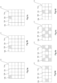
Figure 1 ; - Figs. 3a, 3b and 3c
- represent schematic views of the operation of the solid-state optical sensor of
Figure 1 ; - Figs. 4a, 4b, 4c and 4d
- represent schematic views of the operation of an embodiment variant of an optical solid-state sensor according to the invention;
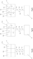
- Fig. 5a
- represents a schematic view of the operation of an optical solid-state sensor with enablement made by a control unit;
- Fig. 5b
- represents a schematic view of the operation of a solid-state optical sensor with "decentralized" enablement; and
- Fig. 5c
- represents a schematic view of the operation of a solid-state optical sensor with "cyclic" enablement.
- With reference to the aforesaid figures, an optical solid-state sensor according to the invention is indicated as a whole with the
number 10. Thisoptical sensor 10, clearly visible infigures 1 and2 , is configured to detect the incidence of one or more photons of a light radiation R during an acquisition window Ta. Saidoptical sensor 10 comprises asilicon plate 11, also represented infigures 1 and2 . - Said
silicon plate 11 comprises in turn asensitive surface 11a configured to detect the incidence of one or more photons of the light radiation R and on which a plurality ofphotosensitive microcells photosensitive microcells sensitive surface 11a according to a first embodiment example of the invention is clearly visible inFigures 1 ,2 ,3a, 3b and 3c . - In this embodiment of the invention, the
photosensitive microcells sensitive surface 11a with a matrix structure of five rows and five columns. -
Figures 4a, 4b, 4c and 4d represent another distribution of thephotosensitive microcells photosensitive microcells sensitive surface 11a with a matrix structure of three rows and five columns. - However, it cannot be ruled out that, in other embodiments of the invention, there is a different number of
photosensitive microcells - Each microcell of such a plurality of
photosensitive microcells optical sensor 10 also comprises acontrol unit 14, clearly visible infigures 1 and2 , configured to acquire such electrical detection signals Ua, Ub, Uc in input. Furthermore, in these embodiment examples of the invention, such acontrol unit 14 is capable of processing such electrical detection signals Ua, Ub, Uc and is configured to generate at least one output electrical signal V obtained from a processing of such electrical detection signals Ua, Ub, Uc. - It is important to point out that the application of the correct polarization voltage to the ends of a photosensitive microcell of such a plurality of
photosensitive microcells - It is also important to point out that only the active microcells of such a plurality of
photosensitive microcells photosensitive microcells - The
optical sensor 10, according to the invention, is configured to perform the following operating steps: - a) activating at least one microcell of the plurality of
photosensitive microcells - b) waiting for the generation of one of the electrical detection signals Ua, Ub, Uc by said at least one active microcell;
- c) activating at least one different inactive microcell by means of said electrical enable signal Ea, Eb, Ec when one of said electrical detection signals Ua, Ub, Uc has been generated;
- d) repeating steps b) and c) for the duration of the acquisition window Ta.
- In the aforesaid first embodiment example of the invention, schematically represented in
Figure 3a , at the beginning of the acquisition window Ta, only onemicrocell 12a is active, while the remaining microcells are kept inactive by theoptical sensor 10. After activating themicrocell 12a, theoptical sensor 10 waits for saidmicrocell 12a to detect a photon and then to generate the corresponding electrical detection signal Ua. When this electrical detection signal Ua is generated by themicrocell 12a, themicrocell 12a will be inactive, while themicrocell 12b will be activated by theoptical sensor 10. After activation of themicrocell 12b, schematically represented inFigure 3b , theoptical sensor 10 waits for saidmicrocell 12b to detect a photon and then to generate the corresponding electrical detection signal Ub. When such an electrical detection signal Ub is generated by themicrocell 12b, themicrocell 12b will be inactive, while a different inactive microcell will be activated by theoptical sensor 10, for example 12c as represented inFigure 3c . - In the aforesaid second embodiment example, schematised at the beginning of the acquisition window Ta in
Figure 4a , two photosensitive microcells are active, while the remaining microcells are kept inactive by theoptical sensor 10. Like in the previous schematisations ofFigure 3a, 3b and 3c , the active microcells are identified with an internal hatch. When an electrical detection signal is generated by the active microcells, these active microcells will then be inactive, while a combination of microcells will be activated by theoptical sensor 10, for example according to the schematisation offigure 4b . The light radiation detection procedure R then continues as schematised inFigure 4c and 4d . - This first embodiment example shows how an
optical sensor 10 according to the invention solves the problem related to the "pile-up distortion" phenomenon, since only a part of the plurality ofphotosensitive microcells optical sensor 10 is active at each instant of the acquisition window Ta. - In particular, according to a first embodiment of the
optical sensor 10 according to the invention, represented infigure 5a , the enablement of the microcells is carried out by thecontrol unit 14 which is capable of controlling the instant of activation of each of said plurality ofphotosensitive microcells control unit 14 will activate a different inactive microcell by means of an electrical enable signal Ea, Eb, Ec. - In a different embodiment of the invention, represented in
Figure 5b , thecontrol unit 14 is capable of controlling the instant of activation of at least one of such plurality ofphotosensitive microcells photosensitive microcells Figure 5b , also act as electrical enable signals Ea, Eb, Ec, being directly responsible for the activation of inactive microcells. - A variant of the latter embodiment of the invention still provides that each of said photosensitive microcells is connected in series to at least one different photosensitive microcell, as represented in
Figure 5c . This allows to obtain a "cyclic" enablement of the photosensitive microcells that does not limit the acquisition window Ta to a single activation of each microcell, allowing the last microcell of the series to control the instant of activation of the first microcell in the series. In particular, the last microcell of the series, in conjunction with the generation of the corresponding electrical detection signal, will generate an electrical enable signal Ea' enabling themicrocell 12a again. - In one embodiment of the invention, after the generation of an electrical detection signal, for example Ua, the activation of a different inactive microcell, for example 12b, takes place after a latency time Td. This latency time Td allows to extend the duration of the acquisition window Ta and adapt this window to the time duration of the light radiation R that is to be detected.
- However, it is not excluded that according to a variant of such an embodiment of the invention, after the generation of an electrical detection signal, for example Ua, the activation of a different inactive microcell, for example 12b, takes place almost instantaneously.
- Each microcell of such a plurality of
photosensitive microcells Figures 1 and2 . Each microcell of such a plurality ofphotosensitive microcells Photon Avalanche Diode - Other embodiments of the invention, not represented for simplicity's sake, involve the use of a plurality of Single-Photon Avalanche Diodes in each microcell. In this case, the sensitivity of each
photosensitive microcell - A device for measuring 100 a distance d, clearly visible in
Figure 2 , comprising at least oneoptical sensor 10 as described above, is also an object of the invention. In particular, said measuringdevice 100 comprises emission means 110, visible infigure 2 , of a light radiation R configured to emit said light radiation R with a duration equal to an emission window Te in the direction of a reference object O. In the present embodiment example of the invention, such emission means 110 comprise a laser emitter. - Furthermore, said measuring
device 100 also comprises at least one solid-stateoptical sensor 10, also visible inFigure 2 , configured to detect the incidence of one or more photons of said light radiation R that are reflected by said reference object O in the direction of said at least oneoptical sensor 10 during an acquisition window Ta. In the first embodiment of the invention described herein, such ameasuring device 100 comprises a singleoptical sensor 10. However, the use of a plurality ofoptical sensors 10 cannot be excluded in other embodiments of the invention. - Again in the present embodiment example of the invention, the sum of the latency times Td between the operating steps b) and the operating steps d) applied by said
optical sensor 10 during the emission window Te is greater than or equal to the emission window Te. This ensures that the acquisition window Ta of theoptical sensor 10 is at least equal to, if not greater than, the emission window Te of the emission means 110. In this way, the information contained in the light radiation Rthat is to be detected will be completely acquired by the measuringdevice 100. This information can then be used by the measuringdevice 100 to make a more accurate estimate of the ToF of the light radiation R, and therefore of the distance d that is to be measured. - The measuring
device 100 also comprises anelectronic board 120, still visible infigure 2 , configured to control the emission of such light radiation R with a duration equal to the emission window Te by the emission means 110. Saidelectronic board 120 is arranged to acquire in input at least one electrical signal generated by saidoptical sensor 10 during the acquisition window Ta. Further, theelectronic board 120 is configured to determine the distance between a first point A of saidmeasuring device 100 and a second point B of the reference object O based on said at least one electrical signal. - In the present embodiment example of the invention, the
electronic board 120 is adapted to generate at least one electrical measurement signal S relative to the measured distance d. - The measuring
device 100 further comprises interfacing means 130, clearly visible infigure 2 , configured to allow the initiation of a measurement of said distance d. In addition, said interfacing means 130 are also configured to allow the measured value of said distance d to be displayed. In particular, in the embodiment of the invention described herein, the interfacing means comprise a touch screen control panel through which a user can initiate a measurement of the distance d and display said measured value of the distance d. - It has in practice been established that the invention achieves the intended task and objects. In particular, with the invention, a solid-state optical sensor has been developed that is not affected by the "pile-up distortion" phenomenon during the step of detecting a light radiation. In addition, with the invention a device for measuring a distance has been developed, comprising such a solid-state optical sensor, which is not subject to a measurement error linked to the reflection coefficient of the surface of the reference object whose distance from the device is to be measured.
- The invention thus conceived is susceptible to many modifications and variants, all falling within the same inventive concept; furthermore, all details can be replaced by equivalent technical elements. In practice, the components and the materials used could be of any type, so long as they are compatible with the specific use, as well as the contingent shapes and dimensions, according to requirements and the state of the art.
- Where the features and techniques mentioned in any claim are followed by reference marks, such reference marks are intended to be affixed solely for the purpose of increasing the intelligibility of the claims and consequently such reference marks have no limiting effect on the interpretation of each element identified by way of example by such reference marks.
Claims (12)
- Solid-state optical sensor (10) configured to detect the incidence of one or more photons of a light radiation (R) during an acquisition window (Ta), said optical sensor (10) comprising:- a silicon plate (11) comprising a sensitive surface (11a), said sensitive surface (11a) being configured to detect the incidence of one or more photons of said light radiation (R), said sensitive surface (11) comprising a plurality of photosensitive microcells (12a, 12b, 12c), each microcell of said plurality of photosensitive microcells (12a, 12b, 12c) being adapted to generate respectively an electrical detection signal (Ua, Ub, Uc) when a photon is detected;- a control unit (14) configured to acquire said electrical detection signals (Ua, Ub, Uc) in input;
characterized in that said optical sensor (10) is configured to perform the following operating steps:a) activating at least one microcell of said plurality of photosensitive microcells (12a, 12b, 12c) at the beginning of said acquisition window (Ta) while keeping the remaining microcells inactive;b) waiting for the generation of one of said electrical detection signals (Ua, Ub, Uc) by said at least one active microcell;c) activating at least one different inactive microcell by means of an electrical enable signal (Ea, Eb, Ec) when one of said electrical detection signals (Ua, Ub, Uc) has been generated;d) repeating steps b) and c) for the duration of said acquisition window (Ta). - Optical sensor (10) according to claim 1, characterized in that said control unit (14) is capable of controlling the instant of activation of each of said plurality of photosensitive microcells (12a, 12b, 12c) by means of said electrical enable signal (Ea, Eb, Ec).
- Optical sensor (10) according to claim 1, characterized in that said control unit (14) is capable of controlling the instant of activation of at least one of said plurality of photosensitive microcells (12a, 12b, 12c) by means of said electrical enable signal (Ea, Eb, Ec), at least a first photosensitive microcell of said plurality of photosensitive microcells (12a, 12b, 12c) being connected in series to at least a second photosensitive microcell of said plurality of photosensitive microcells (12a, 12b, 12c), the instant of activation of said at least a second photosensitive microcell of said plurality of photosensitive microcells (12a, 12b, 12c) being controlled directly by said first photosensitive microcell of said plurality of photosensitive microcells (12a, 12b, 12c) by generating one of said electrical detection signals (Ua, Ub, Uc).
- Optical sensor (10) according to claim 3, characterized in that each of said photosensitive microcells of said plurality of photosensitive microcells (12a, 12b, 12c) is connected in series to at least one different photosensitive microcell of said plurality of photosensitive microcells (12a, 12b, 12c).
- Optical sensor (10) according to any one of the preceding claims, characterized in that a latency time (Td) is applied between said operating step b) and said operating step c).
- Optical sensor (10) according to any one of the preceding claims, characterized in that each microcell of said plurality of photosensitive microcells (12a, 12b, 12c) comprises at least one single-photon avalanche diode (13a, 13b, 13c), each of said plurality of photosensitive microcells (12a, 12b, 12c) being adapted to generate one of said electrical detection signals (Ua, Ub, Uc) when a photon is detected by said at least one single-photon avalanche diode (13a, 13b, 13c).
- Optical sensor (10) according to any one of the preceding claims, characterized in that said control unit (14) is capable of processing said electrical detection signals (Ua, Ub, Uc), said control unit (14) being configured to generate at least one electrical output signal (V) obtained by processing said electrical detection signals (Ua, Ub, Uc).
- Device for measuring (100) a distance (d) comprising:- emission means (110) of a light radiation (R) configured to emit said light radiation (R) with a duration equal to an emission window (Te) in the direction of a reference object (O);- at least one solid-state optical sensor (10) configured to detect the incidence of one or more photons of said light radiation (R) reflected from said reference object (O) in the direction of said at least one optical sensor (10) during an acquisition window (Ta);- an electronic board (120) configured to control the emission of said light radiation (R) having a duration equal to said emission window (Te) by said emission means (110), said electronic board (120) being configured to acquire in input at least one electrical signal generated by said at least one optical sensor (10) during said acquisition window (Ta), said electronic board (120) being configured to determine the distance between a first point (A) of said measuring device (100) and a second point (B) of said reference object (O) based on said at least one electrical signal, characterized in that said at least one optical sensor (10) is an optical sensor (10) according to any one of claims 1 to 8.
- Measuring device (100) according to claim 8 in combination with claim 5, characterized in that the sum of the latency times (Td) between said operating steps b) and said operating steps d) applied by said at least one optical sensor (10) during said acquisition window (Ta) is greater than or equal to said emission window (Te).
- Measuring device (100) according to claim 8 or 9, characterized in that said electronic board (120) is configured to generate at least one electrical measuring signal (S) relative to the measured distance (d).
- Measuring device (100) according to any one of claims 8 to 10, characterized by comprising interfacing means (130), said interfacing means (130) being configured to enable the initiation of a measurement of said distance (d).
- Measuring device (100) according to claim 11, characterized in that said interfacing means (130) are configured to allow the measured value of said distance (d) to be displayed.
Priority Applications (1)
| Application Number | Priority Date | Filing Date | Title |
|---|---|---|---|
| EP23150189.1A EP4397992A1 (en) | 2023-01-03 | 2023-01-03 | Solid-state optical sensor and device for measuring a distance comprising said sensor |
Applications Claiming Priority (1)
| Application Number | Priority Date | Filing Date | Title |
|---|---|---|---|
| EP23150189.1A EP4397992A1 (en) | 2023-01-03 | 2023-01-03 | Solid-state optical sensor and device for measuring a distance comprising said sensor |
Publications (1)
| Publication Number | Publication Date |
|---|---|
| EP4397992A1 true EP4397992A1 (en) | 2024-07-10 |
Family
ID=84829613
Family Applications (1)
| Application Number | Title | Priority Date | Filing Date |
|---|---|---|---|
| EP23150189.1A Withdrawn EP4397992A1 (en) | 2023-01-03 | 2023-01-03 | Solid-state optical sensor and device for measuring a distance comprising said sensor |
Country Status (1)
| Country | Link |
|---|---|
| EP (1) | EP4397992A1 (en) |
Citations (2)
| Publication number | Priority date | Publication date | Assignee | Title |
|---|---|---|---|---|
| CN105606232A (en) * | 2016-01-28 | 2016-05-25 | 中国人民解放军信息工程大学 | Optical signal detection realization method and system |
| WO2021258106A1 (en) * | 2020-06-15 | 2021-12-23 | Continental Automotive Systems, Inc. | Lidar system |
-
2023
- 2023-01-03 EP EP23150189.1A patent/EP4397992A1/en not_active Withdrawn
Patent Citations (2)
| Publication number | Priority date | Publication date | Assignee | Title |
|---|---|---|---|---|
| CN105606232A (en) * | 2016-01-28 | 2016-05-25 | 中国人民解放军信息工程大学 | Optical signal detection realization method and system |
| WO2021258106A1 (en) * | 2020-06-15 | 2021-12-23 | Continental Automotive Systems, Inc. | Lidar system |
Similar Documents
| Publication | Publication Date | Title |
|---|---|---|
| CN110888117B (en) | Detecting light using multiple avalanche photodiode elements | |
| CN110308451B (en) | Dual mode stacked photomultiplier suitable for remote time-of-flight applications | |
| US20180210084A1 (en) | Optoelectronic sensor and method of determining the distance of an object in a monitored zone | |
| CN105043539B (en) | Method and device for operating a photodetector | |
| US20210302553A1 (en) | Lidar systems with improved time-to-digital conversion circuitry | |
| JP2019032305A (en) | Photoelectric sensor for measuring distance and method therefor | |
| JP2019049531A (en) | Device for measuring a distance and method for measuring said distance | |
| TW201600875A (en) | Optical proximity sensors with reconfigurable photodiode array | |
| EP4018218B1 (en) | Infrared imaging assembly | |
| JP2018173379A (en) | Photodetector and distance measuring device | |
| KR20160092137A (en) | Controlling method in distance measuring device using TOF | |
| CA3085648C (en) | Arrangement and method for determining a distance of at least one object using light signals | |
| WO2019176752A1 (en) | Light detection device, light detection method and optical distance sensor | |
| CN111624615B (en) | Light Sensor | |
| US20220283307A1 (en) | Depth sensor calibration using internal reflections | |
| WO2020190920A1 (en) | Dynamic range improvements in lidar applications | |
| Jahromi et al. | A single chip laser radar receiver with a 9× 9 SPAD detector array and a 10-channel TDC | |
| CN115201781A (en) | Lidar sensor and method of removing noise therefrom | |
| CN114089355A (en) | Detection device and method | |
| KR20220008717A (en) | Light source device and light emission control | |
| JP7101529B2 (en) | Optical sensors and electronic devices | |
| US12529772B2 (en) | Time-of-flight imaging system and method and computer program for operating a time-of-flight imaging system | |
| EP3977157B1 (en) | High spatial resolution solid-state image sensor with distributed photomultiplier | |
| US20260063799A1 (en) | Time-of-flight detecting device, system, and method | |
| US20250341619A1 (en) | High photon rate spad device |
Legal Events
| Date | Code | Title | Description |
|---|---|---|---|
| PUAI | Public reference made under article 153(3) epc to a published international application that has entered the european phase |
Free format text: ORIGINAL CODE: 0009012 |
|
| STAA | Information on the status of an ep patent application or granted ep patent |
Free format text: STATUS: THE APPLICATION HAS BEEN PUBLISHED |
|
| AK | Designated contracting states |
Kind code of ref document: A1 Designated state(s): AL AT BE BG CH CY CZ DE DK EE ES FI FR GB GR HR HU IE IS IT LI LT LU LV MC ME MK MT NL NO PL PT RO RS SE SI SK SM TR |
|
| STAA | Information on the status of an ep patent application or granted ep patent |
Free format text: STATUS: THE APPLICATION IS DEEMED TO BE WITHDRAWN |
|
| 18D | Application deemed to be withdrawn |
Effective date: 20250111 |