EP4395522A1 - Thermoelectric conversion module and manufacturing method therefor - Google Patents
Thermoelectric conversion module and manufacturing method therefor Download PDFInfo
- Publication number
- EP4395522A1 EP4395522A1 EP22878393.2A EP22878393A EP4395522A1 EP 4395522 A1 EP4395522 A1 EP 4395522A1 EP 22878393 A EP22878393 A EP 22878393A EP 4395522 A1 EP4395522 A1 EP 4395522A1
- Authority
- EP
- European Patent Office
- Prior art keywords
- thermoelectric conversion
- conversion element
- type thermoelectric
- thermal conduction
- type
- Prior art date
- Legal status (The legal status is an assumption and is not a legal conclusion. Google has not performed a legal analysis and makes no representation as to the accuracy of the status listed.)
- Withdrawn
Links
Images

Classifications
-
- H—ELECTRICITY
- H10—SEMICONDUCTOR DEVICES; ELECTRIC SOLID-STATE DEVICES NOT OTHERWISE PROVIDED FOR
- H10N—ELECTRIC SOLID-STATE DEVICES NOT OTHERWISE PROVIDED FOR
- H10N10/00—Thermoelectric devices comprising a junction of dissimilar materials, i.e. devices exhibiting Seebeck or Peltier effects
- H10N10/80—Constructional details
- H10N10/85—Thermoelectric active materials
- H10N10/856—Thermoelectric active materials comprising organic compositions
-
- H—ELECTRICITY
- H10—SEMICONDUCTOR DEVICES; ELECTRIC SOLID-STATE DEVICES NOT OTHERWISE PROVIDED FOR
- H10N—ELECTRIC SOLID-STATE DEVICES NOT OTHERWISE PROVIDED FOR
- H10N10/00—Thermoelectric devices comprising a junction of dissimilar materials, i.e. devices exhibiting Seebeck or Peltier effects
- H10N10/10—Thermoelectric devices comprising a junction of dissimilar materials, i.e. devices exhibiting Seebeck or Peltier effects operating with only the Peltier or Seebeck effects
- H10N10/17—Thermoelectric devices comprising a junction of dissimilar materials, i.e. devices exhibiting Seebeck or Peltier effects operating with only the Peltier or Seebeck effects characterised by the structure or configuration of the cell or thermocouple forming the device
-
- H—ELECTRICITY
- H10—SEMICONDUCTOR DEVICES; ELECTRIC SOLID-STATE DEVICES NOT OTHERWISE PROVIDED FOR
- H10N—ELECTRIC SOLID-STATE DEVICES NOT OTHERWISE PROVIDED FOR
- H10N10/00—Thermoelectric devices comprising a junction of dissimilar materials, i.e. devices exhibiting Seebeck or Peltier effects
- H10N10/01—Manufacture or treatment
-
- H—ELECTRICITY
- H10—SEMICONDUCTOR DEVICES; ELECTRIC SOLID-STATE DEVICES NOT OTHERWISE PROVIDED FOR
- H10N—ELECTRIC SOLID-STATE DEVICES NOT OTHERWISE PROVIDED FOR
- H10N10/00—Thermoelectric devices comprising a junction of dissimilar materials, i.e. devices exhibiting Seebeck or Peltier effects
- H10N10/10—Thermoelectric devices comprising a junction of dissimilar materials, i.e. devices exhibiting Seebeck or Peltier effects operating with only the Peltier or Seebeck effects
- H10N10/13—Thermoelectric devices comprising a junction of dissimilar materials, i.e. devices exhibiting Seebeck or Peltier effects operating with only the Peltier or Seebeck effects characterised by the heat-exchanging means at the junction
-
- H—ELECTRICITY
- H10—SEMICONDUCTOR DEVICES; ELECTRIC SOLID-STATE DEVICES NOT OTHERWISE PROVIDED FOR
- H10N—ELECTRIC SOLID-STATE DEVICES NOT OTHERWISE PROVIDED FOR
- H10N10/00—Thermoelectric devices comprising a junction of dissimilar materials, i.e. devices exhibiting Seebeck or Peltier effects
- H10N10/80—Constructional details
- H10N10/85—Thermoelectric active materials
- H10N10/851—Thermoelectric active materials comprising inorganic compositions
- H10N10/855—Thermoelectric active materials comprising inorganic compositions comprising compounds containing boron, carbon, oxygen or nitrogen
-
- H—ELECTRICITY
- H10—SEMICONDUCTOR DEVICES; ELECTRIC SOLID-STATE DEVICES NOT OTHERWISE PROVIDED FOR
- H10N—ELECTRIC SOLID-STATE DEVICES NOT OTHERWISE PROVIDED FOR
- H10N10/00—Thermoelectric devices comprising a junction of dissimilar materials, i.e. devices exhibiting Seebeck or Peltier effects
- H10N10/80—Constructional details
- H10N10/85—Thermoelectric active materials
- H10N10/857—Thermoelectric active materials comprising compositions changing continuously or discontinuously inside the material
Definitions
- the substrate 2 is, a sheet member made of a resin showing heat resistance and flexibility, and, for example, has a substantially flat plate shape.
- the resin constituting the substrate 2 include a (meth)acrylic based resin, a (meth)acrylonitrile based resin, a polyamide based resin, a polycarbonate based resin, a polyether based resin, a polyester based resin, an epoxy based resin, an organosiloxane based resin, a polyimide based resin, and a polysulfone based resin.
- the thickness of the substrate 2 is, for example, 5 ⁇ m or more and 50 ⁇ m or less.
- thermoelectric conversion region R1 and two conductive regions R2 are defined on the first main face 2a.
- a plurality of thermoelectric conversion groups 3 are provided in the thermoelectric conversion region R1.
- a plurality of conductive parts 4 are provided in each conductive region R2.
- the thermoelectric conversion region R1 is located between the two conductive regions R2 in the first direction D2. The higher the percentage of the thermoelectric conversion region R1 in the first main face 2a is, the higher output of the thermoelectric conversion module 1 is likely to be.
- the thermoelectric conversion region R1 accounts for, for example, 50% or more and 90% or less of the area of the first main face 2a.
- the two conductive regions R2 accounts for, for example, 5% or more and 30% or less of the area of the first main face 2a.
- the thermoelectric conversion module 1 can exhibit excellent output while reliably forming a conductive path connecting the thermoelectric conversion groups 3 to each other.
- thermoelectric conversion part 11 In two thermoelectric conversion parts 11 adjacent to each other in the first direction D2, the second end part 21b of the p-type thermoelectric conversion element 21 included in one thermoelectric conversion part 11 and the second end part 22b of the n-type thermoelectric conversion element 22 included in the other thermoelectric conversion part 11 are in contact with each other.
- the length L1 of the p-type thermoelectric conversion element 21 in the first direction D2 is, for example, 2 mm or more and 10 mm or less. In this case, a temperature gradient can be easily formed inside the p-type thermoelectric conversion element 21.
- the length of the p-type thermoelectric conversion element 21 in the second direction D3 is, for example, 5 mm or more and 30 mm or less. In this case, a sufficient number of thermoelectric conversion parts 11 can be formed on the first main face 2a.
- the thermal conductivity of the p-type thermoelectric conversion element 21 in the in-plane direction is, for example, 0.01 W/mK or more and 40.0 W/mK or less.
- the electrical conductivity of the p-type thermoelectric conversion element 21 is further enhanced.
- the electron acceptor include polystyrene sulfonic acid, polyvinyl sulfonic acid, poly (meth)acrylic acid, polyvinyl sulfonic acid, toluenesulfonic acid, dodecylbenzenesulfonic acid, camphorsulfonic acid, bis(2-ethylhexyl) sulfosuccinate, chlorine, bromine, iodine, phosphorus pentafluoride, arsenic pentafluoride, boron trifluoride, hydrogen chloride, sulfuric acid, nitric acid, tetrafluoroboric acid, perchloric acid, iron(III) chloride, tetracyanoquinodimethane, and the like.
- the electron acceptor may be polystyrene sulfonic acid (PSS).
- PSS polystyrene sulfonic acid
- the carbon nanotube and the conductive resin may aggregate.
- the p-type thermoelectric conversion element 21 may include a porous structure in which carbon nanotubes are bonded to each other by the conductive resin.
- the n-type thermoelectric conversion element 22 is, for example, an n-type semiconductor layer.
- the n-type thermoelectric conversion element 22 includes, for example, a composite of a plurality of organic substances or a composite of an inorganic substance and an organic substance.
- the n-type thermoelectric conversion element 22 is a portion that exhibits n-type by including a dopant in the p-type thermoelectric conversion element 21. Therefore, the n-type thermoelectric conversion element 22 includes a carbon nanotube, a conductive resin, and a dopant.
- dopant means a substance which changes a Seebeck coefficient of a portion to be doped with the dopant.
- thermoelectric conversion material having a positive Seebeck coefficient value has p-type conductivity
- thermoelectric conversion material having a negative Seebeck coefficient value has an n-type material.
- the dopant of the present embodiment contains: a coordination compound capable of dissociating into an anion that is a complex ion (hereinafter, also simply referred to as "anion”) and an alkali metal cation (hereinafter, also simply referred to as "cation”); and a cation scavenger (hereinafter, also simply referred to as "scavenger”).
- anion an anion that is a complex ion
- cation alkali metal cation
- scavenger a cation scavenger
- the dopant may contain plural kinds of at least one of the coordination compound and
- the scavenger contained in the dopant captures the cation to dissociate the anion and the anion changes a carrier of the carbon nanotube from a hole to an electron.
- the anion is a complex ion having a metal atom at the center, it is conceivable that the n-type conversion is significantly performed by an interaction between the metal atom and the carbon nanotube. It is also conceivable to exhibit the above-described effect because the ionic size of the complex ion is large so that the dissociation of the complex ion from the cation captured by the scavenger is favorable.
- the anion is a complex ion.
- the n-type thermoelectric conversion element 22 contains the metal atom derived from the complex ion. Therefore, in the present embodiment, the metal atom remaining in the n-type thermoelectric conversion element 22 can function as an antioxidant.
- the complex ion (anion) obtained by dissociation of the coordination compound may be selected from the group consisting of ferrocyanide ions, ferricyanide ions, tetrachloroferrate(III) ions, tetrachloroferrate(II) ions, tetracyanonickelate(II) ions, tetrachloronickelate(II) ions, tetracyanocobaltate(II) ions, tetrachlorocobaltate(II) ions, tetracyanocuprate(I) ions, tetrachlorocuprate(II) ions, hexacyanochromate(III) ions, tetrahydroxidozincate(II) ions, and tetrahydroxidoaluminate(III) ions.
- ferrocyanide ions may be used.
- the anion is a ferrocyanide ion
- a material having more favorable characteristics is obtained.
- the anion is a ferrocyanide ion
- the iron atom remaining in the n-type thermoelectric conversion element 22 suitably functions as an antioxidant. For this reason, there are tendencies that a change in physical properties over time is further suppressed and the storage stability is further improved.
- the anion may comprise an iron atom. That is, the coordination compound may include the iron atom.
- the anion may be selected, for example, from the group consisting of ferrocyanide ions, ferricyanide ions, tetrachloroferrate(III) ions, and tetrachloroferrate(II) ions.
- the anion containing the iron atom may be ferrocyanide ions.
- the content of the iron atom in the n-type thermoelectric conversion element 22 may be 0.001% by mass or more and 15% by mass or less, may be 0.005% by mass or more and 12% by mass or less, or may be 0.01% by mass or more and 10% by mass or less.
- the content of the iron atom in the n-type thermoelectric conversion element 22 indicates a value measured by, for example, ICP emission spectrometry.
- the coordination compound may be a complex salt.
- the complex salt include potassium ferrocyanide, sodium ferrocyanide, potassium ferricyanide, sodium ferricyanide, potassium tetrachloroferrate(III), sodium tetrachloroferrate(III), potassium tetrachloroferrate(II), sodium tetrachloroferrate(II), and the like.
- the complex salt may be a hydrate.
- the alkali metal cation obtained by dissociation of the coordination compound examples include a sodium ion, a potassium ion, a lithium ion, and the like.
- the coordination compound may include at least one of a ferrocyanide compound and a ferricyanide compound.
- the cation scavenger is not particularly limited as long as it is a substance which is capable of taking in a cation.
- examples of the cation scavenger include a crown ether-based compound, cyclodextrin, calixarene, ethylenediaminetetraacetate, porphyrin, phthalocyanine, derivatives thereof, and the like.
- the cation scavenger is a crown ether-based compound.
- the crown ether-based compound examples include 15-crown-5-ether, 18-crown-6-ether, 12-crown-4-ether, benzo-18-crown-6-ether, benzo-15-crown-5-ether, benzo-12-crown-4-ether, and the like.
- the ring size of the crown ether used as the scavenger is selected in accordance with, for example, the size of the metal ion to be taken in.
- the crown ether-based compound may be an 18-membered crown ether.
- the crown ether-based compound may be a 15-membered ring crown ether. In a case where the metal ion is a lithium ion, the crown ether-based compound may be a 12-membered ring crown ether.
- the crown ether-based compound may contain a benzene ring. In this case, the stability of the crown ether-based compound may be improved.
- Examples of the crown ether-based compound having a benzene ring include benzo-18-crown-6-ether, benzo-15-crown-5-ether, benzo-12-crown-4-ether, and the like.
- a molar ratio (C 2 /C 1 ) of a content C 2 of the scavenger with respect to a content Ci of the cation may be 0.1 or more and 5 or less, 0.3 or more and 3 or less, or 0.5 or more and 2 or less.
- Each of the plurality of conductive parts 4 is a conductive part located on the first main face 2a and is connected to the corresponding thermoelectric conversion group 3.
- Each conductive part 4 may be a semiconductor instead of a conductor.
- the thickness of each conductive part 4 is identical or substantially identical to the thickness T1 of the p-type thermoelectric conversion element 21.
- the conductivity of each conductive part 4 may be equal to or higher than the conductivity of the p-type thermoelectric conversion element 21.
- the thermal conductivity of each conductive part 4 may be equal to or higher than the thermal conductivity of the p-type thermoelectric conversion element 21.
- At least a part of the plurality of conductive parts 4 may have a single-layer structure or a laminated structure.
- the plurality of conductive parts 4 may include an organic conductive layer and a metal conductive layer located on the organic conductive layer.
- the plurality of conductive parts 4 are formed of the identical material as the p-type thermoelectric conversion element 21. Therefore, each conductive parts 4 has identical conductivity type (p-type).
- the plurality of conductive parts 4 include a first conductive part 4a functioning as a terminal connected to the external device and a second conductive part 4b functioning as a conductive path connecting the adjacent thermoelectric conversion groups 3.
- the plurality of conductive parts 4 have two first conductive parts 4a, and the two first conductive parts 4a are located in one conductive region R2. Only the second conductive parts 4b are provided in the other conductive region R2.
- the plurality of thermoelectric conversion groups 3 are connected in series to each other via a plurality of second conductive parts 4b. Thus, when the thermoelectric conversion module 1 is performing thermoelectric conversion, current may flow in series from one first conductive part 4a to the other first conductive part 4a.
- one first conductive part 4a located in one conductive region R2 is connected to one end of the first thermoelectric conversion group 3a in the first direction D2
- one second conductive part 4b located in the other conductive region R2 is connected to the other end of the first thermoelectric conversion group 3a and one end of the second thermoelectric conversion group 3b in the first direction D2.
- each thermal conduction part 5 in a plan view is not particularly limited, and is, for example, a polygonal shape, a circular shape, an elliptical shape, or the like.
- Each thermal conduction part 5 includes, for example, metal (silver, copper, or the like), carbon, resin (for example, silicone resin, epoxy-based resin, (meth) acrylic-based resin), or the like.
- Each thermal conduction part 5 may include a ceramic such as boron nitride, aluminum nitride, or the like that exhibits high thermal conductivity. From the viewpoint of manufacturing efficiency, each thermal conduction part 5 may include the resin described above. In this case, the thermal conduction part 5 may be formed using the resin or a solution containing the resin.
- each thermal conduction part 5 is, for example, 1 W/mK or more and 400 W/mK or less. Accordingly, when the thermoelectric conversion module 1 is heated, heat is favorably transferred to the thermoelectric conversion part 11 via the plurality of thermal conduction parts 5.
- the length T2 of each thermal conduction part 5 along the thickness direction D1 is, for example, 50 ⁇ m or more and 2000 ⁇ m or less.
- the width L2 of each thermal conduction part 5 along the first direction D2 is, for example, 0.5 mm or more and 2.0 mm or less. In these cases, the thermal conduction function of each thermal conduction part 5 can be favorably exhibited.
- the interval S along the first direction D2 is greater than the length L1 of the p-type thermoelectric conversion element 21 in the first direction D2 and the length of the n-type thermoelectric conversion element 22 in the first direction D2, and is 3 mm or more and 15 mm or less.
- the interval S may be greater than or equal to 4 mm, greater than or equal to 5mm, greater than or equal to 6mm, less than or equal to 12 mm, less than or equal to 10 mm, or less than or equal to 8 mm. Alternatively, the interval S may be less than 12 mm or less than 10 mm.
- one thermal conduction part 5 of the two thermal conduction parts 5 illustrated in (b) of FIG. 2 may be referred to as a first thermal conduction part 5a
- the other thermal conduction part 5 adjacent to the first thermal conduction part 5a along the first direction D2 may be referred to as a second thermal conduction part 5b.
- the first thermal conduction part 5a overlaps one end of the first thermoelectric conversion part 11a in the first direction D2.
- the second thermal conduction part 5b is overlapped with the other end of the first thermoelectric conversion part 11a in the first direction D2.
- the first thermal conduction part 5a overlaps the second end part 22b of the n-type thermoelectric conversion element 22 included in the first thermoelectric conversion part 11a
- the second thermal conduction part 5b overlaps the second end part 21b of the p-type thermoelectric conversion element 21 included in the first thermoelectric conversion part 11a.
- the first thermal conduction part 5a overlaps the second end part 21b of the p-type thermoelectric conversion element 21 included in the second thermoelectric conversion part 11b
- the second thermal conduction part 5b overlaps the second end part 22b of the n-type thermoelectric conversion element 22 included in the second thermoelectric conversion part 11b.
- thermoelectric conversion module 1 may further include configurations other than those described above.
- the thermoelectric conversion module 1 may include wiring for electrically connecting another thermoelectric conversion module, wiring for taking out power to an external circuit, and the like.
- a mask 31 is formed on the first main face 2a of the substrate 2 prepared in advance (first step).
- the mask 31 is formed in a predetermined region of the first main face 2a.
- the mask 31 is a resist mask, a masking tape, or the like.
- the mask 31 is formed by known patterning.
- the tape is fixed to the predetermined region.
- a first layer 41 is formed on the first main face 2a (second step).
- a dispersion liquid is dropped onto the first main face 2a by a known method such as an inkjet method, a dispensing method, a doctor-blade method, a screen printing method, a casting method, a dip coating method, or a spray coating method.
- the first layer 41 is formed by drying the dispersion liquid.
- the substrate 2 is heated by placing the substrate 2 on a hotplate set at 25°C or more and 90°C or less for 10 minutes or more and 21,600minutes or less. Thereby, the dispersion liquid is dried to form the first layer 41.
- the dispersion liquid may be dried by housing the substrate 2 in a blowing and drying oven for 10minutes or more and 21,600minutes or less.
- the dispersion liquid used in the second step is, for example, a liquid in which the p-type thermoelectric conversion material is dispersed.
- the dispersion liquid is a liquid in which the carbon nanotube and the conductive resin are dispersed.
- the content of the carbon nanotube in the dispersion liquid is, for example, 20% by mass or more, 25 % by mass or more, 30% by mass or more, or 35 % by mass or more, and 95% by mass or less, 90% by mass or less, 85% by mass or less, or 80% by mass or less based on the total amount of the conductive resin and the carbon nanotube.
- the electrical conductivity of the first layer 41 tends to increase.
- the first liquid includes, for example, the carbon nanotube and a first solvent.
- the concentration of the carbon nanotube in the first solvent is, for example, 0.01% by mass or more and 10% by mass or less.
- the first solvent may be a solvent capable of dispersing the carbon nanotube, and is, for example, a polar liquid or an aqueous solvent.
- the aqueous solvent is water or a mixed solvent of water and an organic solvent.
- the first solvent may be a protic solvent or an aprotic solvent.
- the first solvent examples include water, alcohols (such as methanol and ethanol), amides (such as N, N-dimethylformamide, N, N-dimethylacetamide, and N-methylpyrrolidone), ketones (such as acetone and methyl ethyl ketone), glycols (such as ethylene glycol and diethylene glycol), dimethyl sulfoxide, and acetonitrile, or the like.
- the first solvent may include one or more selected from the group consisting of water, methanol, ethanol, N-methylpyrrolidone, and dimethyl sulfoxide, and may be water.
- the first liquid may further include additives such as a surfactant and an organic binder.
- the second liquid includes, for example, a conductive resin made of PEDOT and PSS (PEDOT/PSS) and a second solvent.
- PEDOT/PSS the content ratio of PEDOT and PSS is not particularly limited.
- the ratio (mass ratio) of PSS to PEDOT is, for example, 1 or more, 1.25 or more, or 1.5 or more, and 30 or less, or 20 or less.
- the second solvent may be a solvent capable of dispersing PEDOT/PSS, and is, for example, a polar liquid or an aqueous solvent.
- the second solvent may be a protic solvent or an aprotic solvent. Specific examples of the second solvent are identical to the specific examples of the first solvent.
- the second solvent may include one or more of the group consisting of water, methanol, and ethanol, and may be water.
- the second liquid may be an aqueous dispersion liquid of PEDOT/PSS.
- the second solvent may be used alone or as a mixture of two or more.
- the second liquid may further include various additives.
- the mask 31 is removed, and then the substrate 2 is immersed in an organic solvent to form the p-type thermoelectric conversion layer 42 (third step).
- the mask 31 is removed by light, a solvent, or the like.
- a solvent or the like that does not affect the dispersion liquid is used.
- the mask 31 is physically peeled off from the substrate 2.
- the entire substrate 2 is immersed in dimethylsulfoxide (DMSO) of the above described organic solvent (immersion treatment).
- DMSO dimethylsulfoxide
- the entire substrate 2 is immersed in dimethylsulfoxide set at room temperature for 1 minute or more and 7,200 minutes or less.
- the substrate 2 may be heated from the second main face 2b side.
- the substrate 2 is heated by placing the substrate 2 on a hotplate set at 25°C or more and 90°C or less for 10 minutes or more and 21,600minutes or less.
- the patterned p-type thermoelectric conversion layer 42 is formed.
- a portion of the p-type thermoelectric conversion layer 42 is to be the n-type thermoelectric conversion element 22 later.
- Another portion of the p-type thermoelectric conversion layer 42 is to be the p-type thermoelectric conversion element 21 later.
- Still another portion of the p-type thermoelectric conversion layer 42 is to be the conductive part 4 later.
- a plurality of thermal conduction parts 5 are formed on the second main face 2b of the substrate 2 (fourth step).
- a high thermal conduction material is coated by a known method such as an inkjet method, a dispensing method, a doctor-blade method, or a screen printing method.
- the plurality of thermal conduction parts 5 are formed by curing the high thermal conduction material by heating.
- the n-type thermoelectric conversion element 22 is formed in a portion 42a by dropping a dopant-containing solution (dopant solution 51) onto the portion 42a of the p-type thermoelectric conversion layer 42 (fifth step).
- the portion 42a of the p-type thermoelectric conversion layer 42 is impregnated with the dopant solution 51 by a known method such as an inkjet method or a dispensing method.
- regions where the dopant solution 51 is dropped and regions where the dopant solution 51 is not dropped are alternately provided.
- the dopant solution 51 is dried so that the portion 42a becomes an n-type thermoelectric conversion element 22.
- the substrate 2 is heated by placing the substrate 2 on a hotplate set at 25°C or more and 90°C or less for 10 minutes or more and 600 minutes or less.
- the solvent contained in the dopant solution 51 is, for example, water, acetonitrile, ethanol, ethylene glycol, dimethyl sulfoxide (DMSO), N-methylpyrrolidone, N, N-dimethylformamide, N, N-dimethylacetamide or the like.
- thermoelectric conversion module 1 in which the plurality of thermoelectric conversion parts 11 are formed is formed.
- the thickness T1 of the p-type thermoelectric conversion element 21 may be 5 ⁇ m or more and 25 ⁇ m or less.
- the thickness T1 of the p-type thermoelectric conversion element 21 may be 5 ⁇ m or more and 25 ⁇ m or less, and the interval S may be 3 mm or more and less than 12 mm. In these cases, it is possible to further improve output per unit area of the thermoelectric conversion module 1.
- Example 1 the polyimide film was fixed on the glass plate in a state where the thermal conduction part faced the glass plate. Subsequently, the glass plate was placed on a hot plate set at 60°C. Subsequently, the dopant solution was dropped onto a portion of the p-type thermoelectric conversion layer functioning as a thermoelectric conversion element. In Example 1, first, the dopant solution was dropped onto the area with the width of 10mm and the length of 3.5 mm. Subsequently, the dopant solution was dropped onto the area with the width of 10 mm and the length of 3.5 mm in the same way after leaving a space with the length of 3.5 mm.
- thermoelectric conversion module in which the p-type thermoelectric conversion element and the n-type thermoelectric conversion element were alternately arranged in series connection was manufactured.
- the thermal conductivity of the p-type thermoelectric conversion element in the in-plane direction was 32 W/mK.
- Example 1 Example 2
- Example 3 Example 4
- Example 5 Example 6 resistance value (normalization value) 101 74 141 255 97 99 open-circuit voltage (normalization value) 167 238 213 267 146 142 short-circuit current (normalization value) 166 320 151 105 150 143 maximum output (normalization value) 291 191 320 279 322 202 maximum output density per unit area (normalization value) 283 186 311 271 258 208
- the maximum output and the maximum output density of each of Examples 1 to 6 were higher than those of Comparative Example 1 and were about twice or more.
- the maximum output of each of Examples 1, 3, 4 and 5 was about 2.8 times or more the maximum output of Comparative Example 1, and the maximum output density of each of Examples 1, 3, 4 and 5 was about 2.5 times or more the maximum output density of Comparative Example 1.
- the maximum output and the maximum output density of each of Comparative Examples 2 to 4 were equal to or lower than those of Comparative Example 1.
Landscapes
- Engineering & Computer Science (AREA)
- Manufacturing & Machinery (AREA)
- Chemical & Material Sciences (AREA)
- Inorganic Chemistry (AREA)
- Cooling Or The Like Of Semiconductors Or Solid State Devices (AREA)
Abstract
Description
- The present disclosure relates to a thermoelectric conversion module and a method for manufacturing the same.
- A thermoelectric conversion element may be used to perform power generation using geothermal heat, exhaust heat of a factory, or the like.
Patent Document 1 discloses an embodiment in which a flexible substrate having a pattern layer composed of resin layers and metal layers is provided on both surfaces of a thermoelectric conversion module having a P-type thermoelectric element material and an N-type thermoelectric element material. InPatent Document 1, a metal layer included in one flexible substrate overlaps one electrode included in the thermoelectric conversion module, and a metal layer included in the other flexible substrate overlaps the other electrode included in the thermoelectric conversion module. In the above embodiment, by setting one flexible substrate to a high temperature state and setting the other flexible substrate to a low temperature state, a temperature difference is generated in a planar direction of the thermoelectric conversion module. Accordingly, an electromotive force is generated in the thermoelectric conversion module. - [Patent Document 1]
Japanese Patent No. 4,895,293 - In order to improve output of the thermoelectric conversion module as described in
Patent Document 1, for example, it is conceivable to increase thermoelectric conversion efficiency by increasing the temperature difference. In order to increase the temperature difference inPatent Document 1, for example, the P-type thermoelectric element material and the N-type thermoelectric element material may be thinned, or the distance between the metal layers may be increased. However, in the former case, the thinner each thermoelectric element material is, the higher the electric resistance of each thermoelectric element material becomes. In the latter case, as the distance increases, the number of elements per unit area decreases. Therefore, in the case the temperature difference is simply increased, output of the thermoelectric conversion module per unit area may rather decrease. - An object of one aspect of the present disclosure is to provide a thermoelectric conversion module capable of improving output per unit area and a method for manufacturing the same.
- A thermoelectric conversion module and a method for manufacturing the same according to one aspect of the present disclosure are as follows.
- [1] A thermoelectric conversion module includes a substrate having a first main face and a second main face located opposite the first main face, a thermoelectric conversion part located on the first main face, and a first thermal conduction part and a second thermal conduction part located on the second main face and adjacent to each other along a first direction orthogonal to a thickness direction of the substrate, where the thermoelectric conversion part has a p-type thermoelectric conversion element and an n-type thermoelectric conversion element arranged along the first direction, a first end part of the p-type thermoelectric conversion element in the first direction is in contact with a first end part of the n-type thermoelectric conversion element in the first direction, wherein in the thickness direction, the first thermal conduction part is overlapped a second end part of the p-type thermoelectric conversion element in the first direction, in the thickness direction, the second thermal conduction part is overlapped with a second end part of the n-type thermoelectric conversion element in the first direction, each thickness of the p-type thermoelectric conversion element and the n-type thermoelectric conversion element is 3 µm or more and 30 µm or less, and an interval between the first thermal conduction part and the second thermal conduction part in the first direction is greater than a length of the p-type thermoelectric conversion element in the first direction and a length of the n-type thermoelectric conversion element in the first direction, and is 3 mm or more and 15 mm or less.
- [2] The thermoelectric conversion module according to [1], where each thickness of the p-type thermoelectric conversion element and the n-type thermoelectric conversion element is 5 µm or more and 25 µm or less.
- [3] The thermoelectric conversion module according to [1] or [2], where each thickness of the p-type thermoelectric conversion element and the n-type thermoelectric conversion element is 5 µm or more and 25 µm or less, and wherein the interval between the first thermal conduction part and the second thermal conduction part in the first direction is 3 mm or more and less than 12 mm.
- [4] The thermoelectric conversion module according to any one of [1] to [3], further includes a first thermoelectric conversion group located on the first main face and having the thermoelectric conversion par,; and a second thermoelectric conversion group located on the first main face and adjacent to the first thermoelectric conversion group along a second direction orthogonal to the thickness direction and the first direction, where the second thermoelectric conversion group has a second thermoelectric conversion part adjacent to the thermoelectric conversion part along the second direction, the second thermoelectric conversion part has a second p-type thermoelectric conversion element and a second n-type thermoelectric conversion element arranged along the first direction, a first end part of the second p-type thermoelectric conversion element in the first direction is in contact with a first end part of the second n-type thermoelectric conversion element in the first direction, the first thermal conduction part and the second thermal conduction part each extend along the second direction, in the thickness direction, the first thermal conduction part is overlapped a second end part of the second n-type thermoelectric conversion element included in the second thermoelectric conversion part in the first direction, and in the thickness direction, the second thermal conduction part is overlapped with a second end part of the second p-type thermoelectric conversion element included in the second thermoelectric conversion part in the first direction.
- [5] The thermoelectric conversion module according to [4], further includes a first conductive part located on the first main face and connected to one end of the first thermoelectric conversion group in the first direction, and a second conductive part located on the first main face and connected to the other end of the first thermoelectric conversion group in the first direction and one end of the second thermoelectric conversion group in the first direction, where each conductivity type of the first conductive part and the second conductive part is identical.
- [6] The thermoelectric conversion module according to any one of [1] to [5], where each width along the first direction of the first thermal conduction part and the second thermal conduction part is 0.5 mm or more and 2.0 mm or less.
- [7] The thermoelectric conversion module according to any one of [1] to [6], where the p-type thermoelectric conversion element includes a carbon nanotube and a conductive resin, and the n-type thermoelectric conversion element includes the carbon nanotube, the conductive resin, a crown ether-based compound, and a coordination compound including iron atom.
- [8] The thermoelectric conversion module according to [7], where the crown ether-based compound has a benzene ring.
- [9] The thermoelectric conversion module according to [7] or [8], where the coordination compound includes at least one of a ferrocyanide compound and a ferricyanide compound.
- [10] The thermoelectric conversion module according to any one of [1] to [9], where each of the substrate, the first thermoelectric conversion part, the second thermoelectric conversion part, the first thermal conduction part, and the second thermal conduction part shows flexibility.
- [11] A method for manufacturing a thermoelectric conversion module according to any one of [1] to [10], including a first step of forming a mask on the first main face of the substrate, a second step of forming a first layer including a p-type thermoelectric conversion material on the first main face, a third step of forming a thermoelectric conversion layer extending along the first direction by immersing the substrate in an organic solvent after removing the mask, a fourth step of forming a plurality of thermal conduction parts on the second main face of the substrate after the third step, and a fifth step of forming an n-type thermoelectric conversion element in a portion of the thermoelectric conversion layer by dripping a dopant solution on the part after the fourth step.
- According to one aspect of the present disclosure, a thermoelectric conversion module capable of improving output per unit area and a method for manufacturing the same may be provided.
-
- [
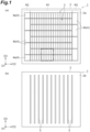
FIG. 1 ] (a) ofFIG. 1 is a schematic plan view illustrating a thermoelectric conversion module according to an embodiment, and (b) ofFIG. 1 is a schematic bottom view illustrating the thermoelectric conversion module according to an embodiment. - [
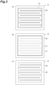
FIG. 2 ] (a) ofFIG. 2 is an enlarged view of a part of (a) ofFIG. 1 , and (b) ofFIG. 2 is a cross-sectional view taken along line IIb-IIb of (a) ofFIG. 2 . - [
FIG. 3 ] (a) to (c) ofFIG. 3 are views for describing a method for manufacturing a thermoelectric conversion module according to an embodiment. - [
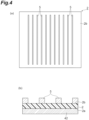
FIG. 4 ] (a) and (b) ofFIG. 4 are views for describing a method for manufacturing a thermoelectric conversion module according to an embodiment. - [
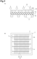
FIG. 5 ] (a) and (b) ofFIG. 5 are views for describing a method for manufacturing a thermoelectric conversion module according to an embodiment. - Hereinafter, an embodiment of the present disclosure will be described in detail with reference to the accompanying drawings. In the following description, the same reference numerals are used for the same element or element having the same function, and redundant description is omitted. In the present specification, "identical" and words similar thereto are not limited to "completely identical".
- First, a configuration of a thermoelectric conversion module according to the present embodiment will be described with reference to
FIGS. 1 and2 . (a) ofFIG. 1 is a schematic plan view showing the thermoelectric conversion module according to the present embodiment, and (b) ofFIG. 1 is a schematic bottom view showing the thermoelectric conversion module according to the present embodiment, (a) ofFIG. 2 is an enlarged view of a part (a region surrounded by an alternate long and short dash line) of (a) ofFIG. 1 . (b) ofFIG. 2 is a cross-sectional view taken along line IIb-IIb of (a) ofFIG. 2 . - The
thermoelectric conversion module 1 shown in (a) and (b) ofFIG. 1 is a device capable of generating power by being supplied with heat from the outside. Thethermoelectric conversion module 1 is a so-called in-plane type device. Thus, thethermoelectric conversion module 1 is likely to be more excellent in workability and flexibility than, for example, a π-type element (cross-plane type element). Therefore, thethermoelectric conversion module 1 can be provided along the side surface of a cylindrical pipe or the like used for recovering factory exhaust heat, for example. That is, thethermoelectric conversion module 1 can be easily disposed at various positions. Therefore, thethermoelectric conversion module 1 is used, for example, as a power source for a plant sensor using exhaust heat. In addition, the contact resistance between the thermoelectric conversion material and the electrode included in thethermoelectric conversion module 1 is likely to be lower than that of the π-type module. In the following, the temperature of each component of thethermoelectric conversion module 1 is measured under natural convection conditions of air. - The
thermoelectric conversion module 1 includes asubstrate 2, a plurality ofthermoelectric conversion groups 3, a plurality ofconductive parts 4, and a plurality ofthermal conduction parts 5. At least one of thesubstrate 2, the plurality ofthermoelectric conversion groups 3, the plurality ofconductive parts 4, and the plurality ofthermal conduction parts 5 shows flexibility. - The
substrate 2 is, a sheet member made of a resin showing heat resistance and flexibility, and, for example, has a substantially flat plate shape. Examples of the resin constituting thesubstrate 2 include a (meth)acrylic based resin, a (meth)acrylonitrile based resin, a polyamide based resin, a polycarbonate based resin, a polyether based resin, a polyester based resin, an epoxy based resin, an organosiloxane based resin, a polyimide based resin, and a polysulfone based resin. The thickness of thesubstrate 2 is, for example, 5 µm or more and 50 µm or less. The thermal conductivity of thesubstrate 2 is, for example, 0.1 W/mK (corresponding to 0.1 watts per meter per Kelvin and 0.1W×m-1 ×K-1) or more and 0.3 W/mK or less. The thermal conductivity of thesubstrate 2 is 0.3 W/mK or less, so that a temperature difference may occur in thethermoelectric conversion group 3. The thermal conductivity of thesubstrate 2 is measured by a steady state method or a non-steady state method. Thesubstrate 2 has a firstmain face 2a and a secondmain face 2b located on the opposite side of the firstmain face 2a. The firstmain face 2a and the secondmain face 2b are surfaces intersecting with a direction along the thickness of thesubstrate 2. The shapes of the firstmain face 2a and the secondmain face 2b is not particularly limited, and are, for example, a polygonal shape, a circular shape, an elliptical shape, or the like. Hereinafter, a direction along the thickness of thesubstrate 2 is simply referred to as a thickness direction D1. Viewing from the thickness direction D1 corresponds to a plan view. Further, directions orthogonal to the thickness direction D1 are referred to as a first direction D2 and a second direction D3. - A thermoelectric conversion region R1 and two conductive regions R2 are defined on the first
main face 2a. A plurality ofthermoelectric conversion groups 3 are provided in the thermoelectric conversion region R1. A plurality ofconductive parts 4 are provided in each conductive region R2. The thermoelectric conversion region R1 is located between the two conductive regions R2 in the first direction D2. The higher the percentage of the thermoelectric conversion region R1 in the firstmain face 2a is, the higher output of thethermoelectric conversion module 1 is likely to be. In a plan view, the thermoelectric conversion region R1 accounts for, for example, 50% or more and 90% or less of the area of the firstmain face 2a. In a plan view, the two conductive regions R2 accounts for, for example, 5% or more and 30% or less of the area of the firstmain face 2a. In this case, thethermoelectric conversion module 1 can exhibit excellent output while reliably forming a conductive path connecting thethermoelectric conversion groups 3 to each other. - Each of the plurality of
thermoelectric conversion groups 3 is a portion capable of generating power by being supplied with heat from the outside, and is located on the firstmain face 2a. Thethermoelectric conversion groups 3 extend along the first direction D2 and are arranged along the second direction D3. Each of thethermoelectric conversion groups 3 has a band shape when viewed from the thickness direction D1. Eachthermoelectric conversion group 3 is electrically connected to each other in series while being spaced apart from each other. In the first direction D2, one end of eachthermoelectric conversion group 3 is connected to one of the plurality ofconductive parts 4 included in one conductive region R2, and the other end of eachthermoelectric conversion group 3 is connected to one of the plurality ofconductive parts 4 included in the other conductive region R2. Each of the plurality ofthermoelectric conversion groups 3 includes a plurality ofthermoelectric conversion parts 11. In the present embodiment, eachthermoelectric conversion group 3 includes tenthermoelectric conversion parts 11, but is not limited thereto. In eachthermoelectric conversion group 3, the plurality ofthermoelectric conversion parts 11 are arranged along the first direction D2. Twothermoelectric conversion parts 11 adjacent to each other in the first direction D2 are in contact with each other and are connected in series. - Hereinafter, one
thermoelectric conversion group 3 of the twothermoelectric conversion groups 3 illustrated in (a) ofFIG. 2 may be referred to as a firstthermoelectric conversion group 3a, and the otherthermoelectric conversion group 3 adjacent to the firstthermoelectric conversion group 3a along the second direction D3 may be referred to as a secondthermoelectric conversion group 3b. Further, thethermoelectric conversion part 11 included in the firstthermoelectric conversion group 3a may be referred to as a firstthermoelectric conversion part 11a, and thethermoelectric conversion part 11 included in the secondthermoelectric conversion group 3b may be referred to as a secondthermoelectric conversion part 11b. A plurality of the firstthermoelectric conversion part 11a included in the firstthermoelectric conversion group 3a are arranged in order along the first direction D2. A plurality of the secondthermoelectric conversion part 11b included in the secondthermoelectric conversion group 3b are arranged in order along the first direction D2. The firstthermoelectric conversion part 11a and the secondthermoelectric conversion part 11b are adjacent to each other along the second direction D3. - Each of the plurality of
thermoelectric conversion parts 11 is a part in which thermoelectric conversion is performed in thethermoelectric conversion module 1, and shows flexibility. The shape of thethermoelectric conversion part 11 in a plan view is not particularly limited, and is, for example, a polygonal shape, a circular shape, an elliptical shape, or the like. Ap-typethermoelectric conversion element 21 and an n-typethermoelectric conversion element 22 have an identical shape as each other, but are not limited thereto. Eachthermoelectric conversion part 11 has the p-typethermoelectric conversion element 21 and the n-typethermoelectric conversion element 22 arranged along the first direction D2. In eachthermoelectric conversion part 11, afirst end part 21a of the p-typethermoelectric conversion element 21 in the first direction D2 and afirst end part 22a of the n-typethermoelectric conversion element 22 in the first direction D2 are in contact with each other. In eachthermoelectric conversion part 11, asecond end part 21b of the p-typethermoelectric conversion element 21 in the first direction D2 is located at one end of the correspondingthermoelectric conversion part 11, and asecond end part 22b of the n-typethermoelectric conversion element 22 in the first direction D2 is located at the other end of the correspondingthermoelectric conversion part 11. In twothermoelectric conversion parts 11 adjacent to each other in the first direction D2, thesecond end part 21b of the p-typethermoelectric conversion element 21 included in onethermoelectric conversion part 11 and thesecond end part 22b of the n-typethermoelectric conversion element 22 included in the otherthermoelectric conversion part 11 are in contact with each other. - In each of the plurality of
thermoelectric conversion groups 3, the p-typethermoelectric conversion element 21 and the n-typethermoelectric conversion element 22 are alternately arranged in the first direction D2. As shown in (a) ofFIG. 2 , in the present embodiment, the p-typethermoelectric conversion element 21 of the firstthermoelectric conversion part 11a is adjacent to the n-type thermoelectric conversion element 22 (second n-type thermoelectric conversion element) of the secondthermoelectric conversion part 11b in the second direction D3, and the n-typethermoelectric conversion element 22 of the firstthermoelectric conversion part 11a is adjacent to the p-type thermoelectric conversion element 21 (second p-type thermoelectric conversion element) of the secondthermoelectric conversion part 11b in the second direction D3. - The p-type
thermoelectric conversion element 21 is provided on the firstmain face 2a of thesubstrate 2 and in contact with the n-typethermoelectric conversion element 22. The thickness T1 of the p-typethermoelectric conversion element 21 is, for example, 3 µm or more and 30 µm or less. Since the thickness T1 is 3µm or more, the electric resistance of the p-typethermoelectric conversion element 21 can be favorably reduced. Since the thickness T1 is 30 µm or less, a temperature gradient can be easily formed inside the p-typethermoelectric conversion element 21. The thickness T1 may be 5 µm or more, 8 µm or more, 10 µm or more, 25 µm or less, 2 µm or less, or 15 µm or less. The length L1 of the p-typethermoelectric conversion element 21 in the first direction D2 is, for example, 2 mm or more and 10 mm or less. In this case, a temperature gradient can be easily formed inside the p-typethermoelectric conversion element 21. The length of the p-typethermoelectric conversion element 21 in the second direction D3 is, for example, 5 mm or more and 30 mm or less. In this case, a sufficient number ofthermoelectric conversion parts 11 can be formed on the firstmain face 2a. The thermal conductivity of the p-typethermoelectric conversion element 21 in the in-plane direction is, for example, 0.01 W/mK or more and 40.0 W/mK or less. The thermal conductivity of the p-typethermoelectric conversion element 21 in the in-plane direction is measured by, for example, an alternating current method, a 3-omega method, or a laser flash method. The p-typethermoelectric conversion element 21 is formed by, for example, various dry methods or wet methods. Examples of the wet method include a doctor blade method, a dip coating method, a spray coating method, a spin coating method, and an ink jet method or the like. - The p-type
thermoelectric conversion element 21 is, for example, a p-type semiconductor layer. The p-typethermoelectric conversion element 21 includes, for example, carbon nanotubes (CNTs) and conductive resin different from the carbon nanotubes. The carbon nanotube exhibits p-type. The carbon nanotube may be single-walled, double-walled, or multi-walled. From the viewpoint of the electrical conductivity of the p-typethermoelectric conversion element 21, single-walled carbon nanotubes (SWCNTs) may be used. The percentage of the single-walled carbon nanotube in the total amount of the carbon nanotube may be 25% by mass or more, 50% by mass or more, or 100% by mass. The diameter of the single-walled carbon nanotube is not particularly limited, and is, for example, 20 nm or less, 10 nm or less, or 3 nm or less. The lower limit of the diameter of the single-walled carbon nanotube is also not particularly limited, but may be 0.4 nm or more, or may be 0.5 nm or more. The thermal conductivity of the carbon nanotube in the in-plane direction may be, for example, 5 W/mK or more and 40 W/mK or less, or 30 W/mK or more and 40 W/mK or less. - In the present specification, the diameter of the single-walled carbon nanotube can be determined by formula: "Diameter (nm) = 248/ω" using the wave number (ω (cm-1)) of a peak appearing at 100 to 300 cm-1 by Raman spectroscopy. As a method for evaluating the single-walled carbon nanotube, a G/D ratio in laser Raman spectroscopy is known. In the present embodiment, the G/D ratio of the single-walled carbon nanotube in laser Raman spectroscopy at a wavelength of 532 nm may be 10 or more or 20 or more. By using such a single-walled carbon nanotube, there is a tendency that the p-type
thermoelectric conversion element 21 having further excellent electrical conductivity is obtained. Note that, the upper limit of the G/D ratio is not particularly limited, and may be, 500 or less or 300 or less. - The content of the carbon nanotube in the p-type
thermoelectric conversion element 21 may be, for example, 20 parts by mass or more, 30 parts by mass or more, 40 parts by mass or more, 99 parts by mass or less, 95 parts by mass or less, or 90 parts by mass or less with respect to 100 parts by mass of the material (p-type thermoelectric conversion material) constituting the p-typethermoelectric conversion element 21. - The conductive resin of the present embodiment is not particularly limited, and a known conductive resin can be used without particular limitation. Examples of the conductive resin include those including a polyaniline-based conductive resin, a polythiophene-based conductive resin, a polypyrrole -based conductive resin, a polyacetylene-based conductive resin, a polyphenylene-based conductive resin, a polyphenylenevinylene-based conductive resin, and the like. As the polythiophene-based conductive resin, poly (3, 4-ethylenedioxythiophene) (PEDOT) can be exemplified. In the present embodiment, the conductive resin includes PEDOT and an electron acceptor. In this case, there is a tendency that the electrical conductivity of the p-type
thermoelectric conversion element 21 is further enhanced. Examples of the electron acceptor include polystyrene sulfonic acid, polyvinyl sulfonic acid, poly (meth)acrylic acid, polyvinyl sulfonic acid, toluenesulfonic acid, dodecylbenzenesulfonic acid, camphorsulfonic acid, bis(2-ethylhexyl) sulfosuccinate, chlorine, bromine, iodine, phosphorus pentafluoride, arsenic pentafluoride, boron trifluoride, hydrogen chloride, sulfuric acid, nitric acid, tetrafluoroboric acid, perchloric acid, iron(III) chloride, tetracyanoquinodimethane, and the like. In view of the electrical conductivity of the p-typethermoelectric conversion element 21, the electron acceptor may be polystyrene sulfonic acid (PSS). In the p-typethermoelectric conversion element 21, the carbon nanotube and the conductive resin may aggregate. The p-typethermoelectric conversion element 21 may include a porous structure in which carbon nanotubes are bonded to each other by the conductive resin. - The n-type
thermoelectric conversion element 22 is provided on the firstmain face 2a of thesubstrate 2 and is in contact with the p-typethermoelectric conversion element 21. The thickness of the n-typethermoelectric conversion element 22 is identical to or substantially identical to the thickness T1 of the p-typethermoelectric conversion element 21. The length of the n-typethermoelectric conversion element 22 in the first direction D2 is identical to or substantially identical to the length L1 of the p-typethermoelectric conversion element 21. The length of the n-typethermoelectric conversion element 22 in the second direction D3 is, for example, 2 mm or more and 10 mm or less. In this case, a sufficient number ofthermoelectric conversion parts 11 can be formed on the firstmain face 2a. The thermal conductivity of the n-typethermoelectric conversion element 22 in the in-plane direction is, for example, 0.01 W/mK or more and 40.0 W/mK or less. The thermal conductivity of the n-typethermoelectric conversion element 22 in the in-plane direction is measured by, for example, an alternating current method, a 3-omega method, or a laser flash method. As same as the p-typethermoelectric conversion element 21, the n-typethermoelectric conversion element 22 is formed by, for example, various dry methods or wet methods. - The n-type
thermoelectric conversion element 22 is, for example, an n-type semiconductor layer. The n-typethermoelectric conversion element 22 includes, for example, a composite of a plurality of organic substances or a composite of an inorganic substance and an organic substance. In the present embodiment, the n-typethermoelectric conversion element 22 is a portion that exhibits n-type by including a dopant in the p-typethermoelectric conversion element 21. Therefore, the n-typethermoelectric conversion element 22 includes a carbon nanotube, a conductive resin, and a dopant. In the present embodiment, dopant means a substance which changes a Seebeck coefficient of a portion to be doped with the dopant. The expression "changing a Seebeck coefficient" means decreasing a Seebeck coefficient value or changing a Seebeck coefficient value from a positive value to a negative value. A thermoelectric conversion material having a positive Seebeck coefficient value has p-type conductivity, and a thermoelectric conversion material having a negative Seebeck coefficient value has an n-type material. - The dopant of the present embodiment, for example, contains: a coordination compound capable of dissociating into an anion that is a complex ion (hereinafter, also simply referred to as "anion") and an alkali metal cation (hereinafter, also simply referred to as "cation"); and a cation scavenger (hereinafter, also simply referred to as "scavenger"). Within the n-type
thermoelectric conversion element 22, at least a part of the coordination compound may be dissociated into the anion and the cation. In this case, the cation may be captured by the scavenger. The dopant may contain plural kinds of at least one of the coordination compound and a scavenger. In the portion where the p-typethermoelectric conversion element 21 contains the dopant, the Seebeck coefficient changes. As a result, the n-typethermoelectric conversion element 22 is formed in the above portion. - The reason why the above-described effect is exhibited is not particularly limited, and as one of the causes it is conceivable that the scavenger contained in the dopant captures the cation to dissociate the anion and the anion changes a carrier of the carbon nanotube from a hole to an electron. At this time, in the present embodiment, since the anion is a complex ion having a metal atom at the center, it is conceivable that the n-type conversion is significantly performed by an interaction between the metal atom and the carbon nanotube. It is also conceivable to exhibit the above-described effect because the ionic size of the complex ion is large so that the dissociation of the complex ion from the cation captured by the scavenger is favorable. In the dopant of the present embodiment, the anion is a complex ion. Thus, the n-type
thermoelectric conversion element 22 contains the metal atom derived from the complex ion. Therefore, in the present embodiment, the metal atom remaining in the n-typethermoelectric conversion element 22 can function as an antioxidant. - The complex ion (anion) obtained by dissociation of the coordination compound may be selected from the group consisting of ferrocyanide ions, ferricyanide ions, tetrachloroferrate(III) ions, tetrachloroferrate(II) ions, tetracyanonickelate(II) ions, tetrachloronickelate(II) ions, tetracyanocobaltate(II) ions, tetrachlorocobaltate(II) ions, tetracyanocuprate(I) ions, tetrachlorocuprate(II) ions, hexacyanochromate(III) ions, tetrahydroxidozincate(II) ions, and tetrahydroxidoaluminate(III) ions. Among these, ferrocyanide ions may be used. When the anion is a ferrocyanide ion, a material having more favorable characteristics is obtained. Furthermore, when the anion is a ferrocyanide ion, the iron atom remaining in the n-type
thermoelectric conversion element 22 suitably functions as an antioxidant. For this reason, there are tendencies that a change in physical properties over time is further suppressed and the storage stability is further improved. - The anion may comprise an iron atom. That is, the coordination compound may include the iron atom. In this case, the anion may be selected, for example, from the group consisting of ferrocyanide ions, ferricyanide ions, tetrachloroferrate(III) ions, and tetrachloroferrate(II) ions. In view of the characteristics of the n-type
thermoelectric conversion element 22, the anion containing the iron atom may be ferrocyanide ions. From the viewpoint of the antioxidant effect, the content of the iron atom in the n-typethermoelectric conversion element 22 may be 0.001% by mass or more and 15% by mass or less, may be 0.005% by mass or more and 12% by mass or less, or may be 0.01% by mass or more and 10% by mass or less. The content of the iron atom in the n-typethermoelectric conversion element 22 indicates a value measured by, for example, ICP emission spectrometry. - The coordination compound may be a complex salt. Examples of the complex salt include potassium ferrocyanide, sodium ferrocyanide, potassium ferricyanide, sodium ferricyanide, potassium tetrachloroferrate(III), sodium tetrachloroferrate(III), potassium tetrachloroferrate(II), sodium tetrachloroferrate(II), and the like. The complex salt may be a hydrate.
- Examples of the alkali metal cation obtained by dissociation of the coordination compound include a sodium ion, a potassium ion, a lithium ion, and the like. The coordination compound may include at least one of a ferrocyanide compound and a ferricyanide compound.
- The cation scavenger is not particularly limited as long as it is a substance which is capable of taking in a cation. Examples of the cation scavenger include a crown ether-based compound, cyclodextrin, calixarene, ethylenediaminetetraacetate, porphyrin, phthalocyanine, derivatives thereof, and the like. In the present embodiment, the cation scavenger is a crown ether-based compound. Examples of the crown ether-based compound include 15-crown-5-ether, 18-crown-6-ether, 12-crown-4-ether, benzo-18-crown-6-ether, benzo-15-crown-5-ether, benzo-12-crown-4-ether, and the like. The ring size of the crown ether used as the scavenger is selected in accordance with, for example, the size of the metal ion to be taken in. For example, in a case where the metal ion is a potassium ion, the crown ether-based compound may be an 18-membered crown ether. In a case where the metal ion is a sodium ion, the crown ether-based compound may be a 15-membered ring crown ether. In a case where the metal ion is a lithium ion, the crown ether-based compound may be a 12-membered ring crown ether.
- The crown ether-based compound may contain a benzene ring. In this case, the stability of the crown ether-based compound may be improved. Examples of the crown ether-based compound having a benzene ring include benzo-18-crown-6-ether, benzo-15-crown-5-ether, benzo-12-crown-4-ether, and the like.
- A molar ratio (C2/C1) of a content C2 of the scavenger with respect to a content Ci of the cation may be 0.1 or more and 5 or less, 0.3 or more and 3 or less, or 0.5 or more and 2 or less.
- Each of the plurality of
conductive parts 4 is a conductive part located on the firstmain face 2a and is connected to the correspondingthermoelectric conversion group 3. Eachconductive part 4 may be a semiconductor instead of a conductor. The thickness of eachconductive part 4 is identical or substantially identical to the thickness T1 of the p-typethermoelectric conversion element 21. The conductivity of eachconductive part 4 may be equal to or higher than the conductivity of the p-typethermoelectric conversion element 21. The thermal conductivity of eachconductive part 4 may be equal to or higher than the thermal conductivity of the p-typethermoelectric conversion element 21. At least a part of the plurality ofconductive parts 4 may have a single-layer structure or a laminated structure. For example, at least a part of the plurality ofconductive parts 4 may include an organic conductive layer and a metal conductive layer located on the organic conductive layer. In the present embodiment, the plurality ofconductive parts 4 are formed of the identical material as the p-typethermoelectric conversion element 21. Therefore, eachconductive parts 4 has identical conductivity type (p-type). - The plurality of
conductive parts 4 include a firstconductive part 4a functioning as a terminal connected to the external device and a secondconductive part 4b functioning as a conductive path connecting the adjacentthermoelectric conversion groups 3. The plurality ofconductive parts 4 have two firstconductive parts 4a, and the two firstconductive parts 4a are located in one conductive region R2. Only the secondconductive parts 4b are provided in the other conductive region R2. The plurality ofthermoelectric conversion groups 3 are connected in series to each other via a plurality of secondconductive parts 4b. Thus, when thethermoelectric conversion module 1 is performing thermoelectric conversion, current may flow in series from one firstconductive part 4a to the other firstconductive part 4a. For example, one firstconductive part 4a located in one conductive region R2 is connected to one end of the firstthermoelectric conversion group 3a in the first direction D2, and one secondconductive part 4b located in the other conductive region R2 is connected to the other end of the firstthermoelectric conversion group 3a and one end of the secondthermoelectric conversion group 3b in the first direction D2. - The plurality of
thermal conduction parts 5 are portions exhibiting higher thermal conductivity than thesubstrate 2, and are located on the secondmain face 2b. At least a part of the plurality ofthermal conduction parts 5 overlaps the thermoelectric conversion group 3 (that is, the thermoelectric conversion part 11) in the thickness direction D1. More specifically, at least a part of the plurality ofthermal conduction parts 5 overlaps an end of thethermoelectric conversion part 11. On the other hand, eachthermal conduction part 5 does not overlap the center of thethermoelectric conversion part 11. Accordingly, a temperature gradient inside thethermoelectric conversion part 11 along the first direction D2 may be favorably generated. The plurality ofthermal conduction parts 5 are spaced apart from each other along the first direction D2, and have a band shape extending along the second direction D3 in a plan view. The shape of eachthermal conduction part 5 in a plan view is not particularly limited, and is, for example, a polygonal shape, a circular shape, an elliptical shape, or the like. Eachthermal conduction part 5 includes, for example, metal (silver, copper, or the like), carbon, resin (for example, silicone resin, epoxy-based resin, (meth) acrylic-based resin), or the like. Eachthermal conduction part 5 may include a ceramic such as boron nitride, aluminum nitride, or the like that exhibits high thermal conductivity. From the viewpoint of manufacturing efficiency, eachthermal conduction part 5 may include the resin described above. In this case, thethermal conduction part 5 may be formed using the resin or a solution containing the resin. The thermal conductivity of eachthermal conduction part 5 is, for example, 1 W/mK or more and 400 W/mK or less. Accordingly, when thethermoelectric conversion module 1 is heated, heat is favorably transferred to thethermoelectric conversion part 11 via the plurality ofthermal conduction parts 5. - The length T2 of each
thermal conduction part 5 along the thickness direction D1 is, for example, 50µm or more and 2000µm or less. The width L2 of eachthermal conduction part 5 along the first direction D2 is, for example, 0.5 mm or more and 2.0 mm or less. In these cases, the thermal conduction function of eachthermal conduction part 5 can be favorably exhibited. In two adjacentthermal conduction parts 5, the interval S along the first direction D2 is greater than the length L1 of the p-typethermoelectric conversion element 21 in the first direction D2 and the length of the n-typethermoelectric conversion element 22 in the first direction D2, and is 3 mm or more and 15 mm or less. The interval S may be greater than or equal to 4 mm, greater than or equal to 5mm, greater than or equal to 6mm, less than or equal to 12 mm, less than or equal to 10 mm, or less than or equal to 8 mm. Alternatively, the interval S may be less than 12 mm or less than 10 mm. - Hereinafter, one
thermal conduction part 5 of the twothermal conduction parts 5 illustrated in (b) ofFIG. 2 may be referred to as a firstthermal conduction part 5a, and the otherthermal conduction part 5 adjacent to the firstthermal conduction part 5a along the first direction D2 may be referred to as a secondthermal conduction part 5b. In this case, in the thickness direction D1, the firstthermal conduction part 5a overlaps one end of the firstthermoelectric conversion part 11a in the first direction D2. Further, in the thickness direction D1, the secondthermal conduction part 5b is overlapped with the other end of the firstthermoelectric conversion part 11a in the first direction D2. To be more specific, in the thickness direction D1, the firstthermal conduction part 5a overlaps thesecond end part 22b of the n-typethermoelectric conversion element 22 included in the firstthermoelectric conversion part 11a, and the secondthermal conduction part 5b overlaps thesecond end part 21b of the p-typethermoelectric conversion element 21 included in the firstthermoelectric conversion part 11a. In addition, as shown in (a) ofFIG. 2 , in the thickness direction D1, the firstthermal conduction part 5a overlaps thesecond end part 21b of the p-typethermoelectric conversion element 21 included in the secondthermoelectric conversion part 11b, and the secondthermal conduction part 5b overlaps thesecond end part 22b of the n-typethermoelectric conversion element 22 included in the secondthermoelectric conversion part 11b. - The
thermoelectric conversion module 1 may further include configurations other than those described above. For example, thethermoelectric conversion module 1 may include wiring for electrically connecting another thermoelectric conversion module, wiring for taking out power to an external circuit, and the like. - Next, an example of a method for manufacturing the
thermoelectric conversion module 1 according to the present embodiment will be described with reference toFIGS. 3 to 5 . (a) to (c) ofFIG. 3 , (a) and (b) ofFIG. 4 , and (a) and (b) ofFIG. 5 illustrate a method for manufacturing a thermoelectric conversion module according to the present embodiment. - First, as shown in (a) of
FIG. 3 , amask 31 is formed on the firstmain face 2a of thesubstrate 2 prepared in advance (first step). In the first step, themask 31 is formed in a predetermined region of the firstmain face 2a. Themask 31 is a resist mask, a masking tape, or the like. In the former case, themask 31 is formed by known patterning. In the latter case, the tape is fixed to the predetermined region. - Next, as shown in (b) of
FIG. 3 , afirst layer 41 is formed on the firstmain face 2a (second step). In the second step, first, a dispersion liquid is dropped onto the firstmain face 2a by a known method such as an inkjet method, a dispensing method, a doctor-blade method, a screen printing method, a casting method, a dip coating method, or a spray coating method. Subsequently, thefirst layer 41 is formed by drying the dispersion liquid. For example, thesubstrate 2 is heated by placing thesubstrate 2 on a hotplate set at 25°C or more and 90°C or less for 10 minutes or more and 21,600minutes or less. Thereby, the dispersion liquid is dried to form thefirst layer 41. In the second step, instead of placing thesubstrate 2 on a hotplate, the dispersion liquid may be dried by housing thesubstrate 2 in a blowing and drying oven for 10minutes or more and 21,600minutes or less. - The dispersion liquid used in the second step is, for example, a liquid in which the p-type thermoelectric conversion material is dispersed. In the present embodiment, the dispersion liquid is a liquid in which the carbon nanotube and the conductive resin are dispersed. The content of the carbon nanotube in the dispersion liquid is, for example, 20% by mass or more, 25 % by mass or more, 30% by mass or more, or 35 % by mass or more, and 95% by mass or less, 90% by mass or less, 85% by mass or less, or 80% by mass or less based on the total amount of the conductive resin and the carbon nanotube. In this case, the electrical conductivity of the
first layer 41 tends to increase. In addition, the total mass concentration of the carbon nanotube and the conductive resin in the dispersion liquid is, for example, 0.05% by mass or more, 0.06% by mass or more, 0.07% by mass or more, 0.10% by mass or more, 0.12% by mass or more, or 0.15% by mass or more. The total mass concentration of the carbon nanotube and the conductive resin in the dispersion may be 10% by mass or less, or 2% by mass or less. The dispersion liquid used in the second step is, for example, a mixed liquid formed by mixing a first liquid containing a carbon nanotube and a second liquid containing a conductive resin. - The first liquid includes, for example, the carbon nanotube and a first solvent. The concentration of the carbon nanotube in the first solvent is, for example, 0.01% by mass or more and 10% by mass or less. The first solvent may be a solvent capable of dispersing the carbon nanotube, and is, for example, a polar liquid or an aqueous solvent. The aqueous solvent is water or a mixed solvent of water and an organic solvent. The first solvent may be a protic solvent or an aprotic solvent. Specific examples of the first solvent include water, alcohols (such as methanol and ethanol), amides (such as N, N-dimethylformamide, N, N-dimethylacetamide, and N-methylpyrrolidone), ketones (such as acetone and methyl ethyl ketone), glycols (such as ethylene glycol and diethylene glycol), dimethyl sulfoxide, and acetonitrile, or the like. The first solvent may include one or more selected from the group consisting of water, methanol, ethanol, N-methylpyrrolidone, and dimethyl sulfoxide, and may be water. The first liquid may further include additives such as a surfactant and an organic binder.
- The second liquid includes, for example, a conductive resin made of PEDOT and PSS (PEDOT/PSS) and a second solvent. In the PEDOT/PSS, the content ratio of PEDOT and PSS is not particularly limited. The ratio (mass ratio) of PSS to PEDOT is, for example, 1 or more, 1.25 or more, or 1.5 or more, and 30 or less, or 20 or less. The second solvent may be a solvent capable of dispersing PEDOT/PSS, and is, for example, a polar liquid or an aqueous solvent. The second solvent may be a protic solvent or an aprotic solvent. Specific examples of the second solvent are identical to the specific examples of the first solvent. The second solvent may include one or more of the group consisting of water, methanol, and ethanol, and may be water. In one embodiment, the second liquid may be an aqueous dispersion liquid of PEDOT/PSS. The second solvent may be used alone or as a mixture of two or more. The second liquid may further include various additives.
- Next, as shown in (c) of
FIG. 3 , themask 31 is removed, and then thesubstrate 2 is immersed in an organic solvent to form the p-type thermoelectric conversion layer 42 (third step). For example, in the case where themask 31 is a resist mask, themask 31 is removed by light, a solvent, or the like. In this case, a solvent or the like that does not affect the dispersion liquid is used. For example, in the case where themask 31 is a masking tape, themask 31 is physically peeled off from thesubstrate 2. In the present embodiment, after patterning of thefirst layer 41, theentire substrate 2 is immersed in dimethylsulfoxide (DMSO) of the above described organic solvent (immersion treatment). For example, theentire substrate 2 is immersed in dimethylsulfoxide set at room temperature for 1 minute or more and 7,200 minutes or less. After the immersion treatment, thesubstrate 2 may be heated from the secondmain face 2b side. For example, thesubstrate 2 is heated by placing thesubstrate 2 on a hotplate set at 25°C or more and 90°C or less for 10 minutes or more and 21,600minutes or less. Through the above process, the patterned p-typethermoelectric conversion layer 42 is formed. A portion of the p-typethermoelectric conversion layer 42 is to be the n-typethermoelectric conversion element 22 later. Another portion of the p-typethermoelectric conversion layer 42 is to be the p-typethermoelectric conversion element 21 later. Still another portion of the p-typethermoelectric conversion layer 42 is to be theconductive part 4 later. - Next, as shown (a) and (b) of
FIG. 4 , after the above third step, a plurality ofthermal conduction parts 5 are formed on the secondmain face 2b of the substrate 2 (fourth step). In the fourth step, a high thermal conduction material is coated by a known method such as an inkjet method, a dispensing method, a doctor-blade method, or a screen printing method. Subsequently, the plurality ofthermal conduction parts 5 are formed by curing the high thermal conduction material by heating. - Next, as shown in (a) of
FIG. 5 , after the fourth step, the n-typethermoelectric conversion element 22 is formed in aportion 42a by dropping a dopant-containing solution (dopant solution 51) onto theportion 42a of the p-type thermoelectric conversion layer 42 (fifth step). In the fifth step, theportion 42a of the p-typethermoelectric conversion layer 42 is impregnated with thedopant solution 51 by a known method such as an inkjet method or a dispensing method. In the present embodiment, in the p-typethermoelectric conversion layer 42, regions where thedopant solution 51 is dropped and regions where thedopant solution 51 is not dropped are alternately provided. Subsequently, thedopant solution 51 is dried so that theportion 42a becomes an n-typethermoelectric conversion element 22. For example, thesubstrate 2 is heated by placing thesubstrate 2 on a hotplate set at 25°C or more and 90°C or less for 10 minutes or more and 600 minutes or less. Thus, thedopant solution 51 is dried. The solvent contained in thedopant solution 51 is, for example, water, acetonitrile, ethanol, ethylene glycol, dimethyl sulfoxide (DMSO), N-methylpyrrolidone, N, N-dimethylformamide, N, N-dimethylacetamide or the like. A portion of the p-typethermoelectric conversion layer 42 to which thedopant solution 51 is not dropped becomes the p-typethermoelectric conversion element 21 or theconductive part 4 as illustrated in (b) ofFIG. 5 . As described above, thethermoelectric conversion module 1 in which the plurality ofthermoelectric conversion parts 11 are formed is formed. - Next, operations and effects achieved by the
thermoelectric conversion module 1 formed by the manufacturing method according to the present embodiment described above will be described. - The
thermoelectric conversion module 1 according to the present embodiment includes the firstthermal conduction part 5a and the secondthermal conduction part 5b, in the thickness direction D1, the firstthermal conduction part 5a overlaps thesecond end part 22b of the n-typethermoelectric conversion element 22 included in the firstthermoelectric conversion part 11a, and in the thickness direction D1, the secondthermal conduction part 5b overlaps thesecond end part 21b of the p-typethermoelectric conversion element 21 included in the firstthermoelectric conversion part 11a. In addition, the interval S between the firstthermal conduction part 5a and the secondthermal conduction part 5b in the first direction D2 is larger than the length L1 of the p-typethermoelectric conversion element 21 in the first direction D2 and the length of the n-typethermoelectric conversion element 22 in the first direction D2. Accordingly, each of the firstthermal conduction part 5a and the secondthermal conduction part 5b overlaps both ends of the firstthermoelectric conversion part 11a in the thickness direction D1, whereas does not overlap the center of the firstthermoelectric conversion part 11a. Therefore, for example, by heating the firstthermal conduction part 5a and the secondthermal conduction part 5b, an internal temperature difference can be generated in each of the p-typethermoelectric conversion element 21 and the n-typethermoelectric conversion element 22. Herein, the interval S is 3 mm or more and 15 mm or less, and the thickness T1 of the p-type thermoelectric conversion element 21 (and the thickness of the n-type thermoelectric conversion element 22) is 3 µm or more and 30 µm or less. Since the interval S and the thickness T1 are within the above ranges, it is possible to suppress an increase in the number of elements per unit area and an internal resistance of the element while realizing an increase in the temperature difference due to the firstthermal conduction part 5a and the secondthermal conduction part 5b described above. Therefore, by adopting thethermoelectric conversion module 1 according to the present embodiment, it is possible to realize an output improvement per unit area. - In the present embodiment, the thickness T1 of the p-type
thermoelectric conversion element 21 may be 5 µm or more and 25 µm or less. Alternatively, the thickness T1 of the p-typethermoelectric conversion element 21 may be 5 µm or more and 25 µm or less, and the interval S may be 3 mm or more and less than 12 mm. In these cases, it is possible to further improve output per unit area of thethermoelectric conversion module 1. - In the present embodiment, the width L2 of each
thermal conduction part 5 along the first direction D2 may be 0.5 mm or more and 2.0 mm or less. In this case, the heat transfer performance by eachthermal conduction part 5 is favorably exhibited, and the internal temperature difference of thethermoelectric conversion part 11 can be increased. - In the present embodiment, each of the
substrate 2, thethermoelectric conversion part 11, and thethermal conduction part 5 may show flexibility. In this case, for example, thethermoelectric conversion module 1 can be easily provided along the surface of the cylindrical pipe. That is, it is possible to relax the restriction on the mounting place of thethermoelectric conversion module 1. - In the present embodiment, the
dopant solution 51 is dropped onto theportion 42a of the p-typethermoelectric conversion layer 42 to make theportion 42a become the n-typethermoelectric conversion element 22. In this case, the contact resistance between the p-typethermoelectric conversion element 21 and the n-typethermoelectric conversion element 22 can be favorably reduced. Dropping of thedopant solution 51 is performed after formation of thethermal conduction part 5. Thus, the material contained in thedopant solution 51 is less likely to be deteriorated by heating or the like. - The thermoelectric conversion module and the manufacturing method thereof according to the present disclosure are not limited to the above-described embodiment, and various other modifications are possible. For example, although the thermoelectric conversion element is exposed on the first main face in the above-described embodiment, the present disclosure is not limited thereto. For example, the thermoelectric conversion element may be covered with a resinous sealing layer or the like. In addition, an insulator may be provided between two adjacent thermoelectric conversion groups. In this case, from the viewpoint of maintaining the internal temperature difference of the thermoelectric conversion element, the thermal conductivity of the insulator may be low.
- In the above-described embodiment, a space is present between two adjacent thermal conduction parts, but the present disclosure is not limited thereto. For example, an insulator may be provided between two adjacent thermal conduction parts. In this case, from the viewpoint of maintaining the internal temperature difference of the thermoelectric conversion element, the thermal conductivity of the insulator may be low.
- One aspect of the present disclosure will be described in more detail with the following examples, but one aspect of the present disclosure is not limited to these examples.
- 80 g of the carbon nanotube dispersion liquid (concentration: 0.2% by mass, G/D ratio: 41, aqueous dispersion liquid, single-walled carbon nanotubes, diameters: 0.9 to 1.7nm) was concentrated by evacuation until the carbon nanotube concentration became 0.4% by mass. Subsequently, 3.6g of PEDOT/PSS aqueous dispersion liquid ("Clevious (registered trademark) PH1000" manufactured by Heraeus Holding, solid content concentration: 1.2% by mass) and the concentrated carbon nanotube dispersion liquid were sufficiently stirred with a three one motor ("PM203 type" manufactured by AS ONECORPORATION) (stirring time: 30minutes). Subsequently, the stirred liquid was sufficiently defoamed with a planetary centrifugal mixer ("THINKY MIXER ARE-310" manufactured by THINKY CORPORATION) (treatment time: 3 minutes). Thus, a dispersion liquid in which the content of the carbon nanotube was 75% by mass with respect to the total amount of the PEDOT/PSS and the carbon nanotubes was prepared. The viscosity of the dispersion liquid at a shear rate of 0.01s-1 was 1,320,000mPa- sec. The viscosity of the dispersion liquid was measured using a rheometer ("MCR302" (product name) manufactured by Anton Paar GmbH). The measurement conditions were as follows: 25°C of temperature, ϕ 25 mm parallel plate of plate, 1 mm of gap.
- 0.32 g of potassium ferrocyanide trihydrate and 0.94 g of benzo-18-crown-6-ether were dissolved in 15 mL of ultrapure water to obtain a dopant solution. The concentrations of potassium ions and benzo-18-crown-6-ether in the dopant solution were 0.2M, respectively.
- A double-sided tape (manufactured by NICHIBAN Co., Ltd., NICETACK Lower Adhesion type) was attached to four sides of a 100mm square glass plate. Further, A spray adhesive (Regular Series S/N 55 manufactured by 3M Japan Limited) was applied to the glass plate. In addition, a 100mm square polyimide film (manufactured by DU PONT-TORAY Co., Ltd., Kapton H type, film thickness of 25 µm, and thermal conductivity of 0. 16 W/mK) was prepared as a substrate material. Subsequently, the protective sheet of the double-sided tape attached to the glass plate was peeled off, and then the polyimide film was attached to the glass plate. Subsequently, the polyimide film was washed with acetone. Subsequently, a masking tape (Micron Masking Tape with width of 1mm manufactured by AIZU PROJECT Co., Ltd.) was attached to a predetermined position on the polyimide film. In addition, a polyimide tape was attached to edge part of the polyimide film and the glass plate. Thus, a laminated body of the polyimide film and the glass plate, which functioning as a substrate, was formed.
- The dispersion liquid was dropped onto the polyimide film, and the polyimide film was coated with the dispersion liquid using a doctor-blade having a gap of 2.8 mm. Subsequently, the laminated body coated with the dispersion liquid was placed in a blowing and drying oven set at 60°C for 3 hours. In this manner, a composite film having a thickness of 62 µm was formed on the polyimide film. The composite film is provided in both of a thermoelectric conversion region where thermoelectric conversion elements are to be provided on the polyimide film later and a conductive region where conductive parts are to be provided on the polyimide film later. Then, the masking tape was removed. As a result, the composite film was patterned. In the thermoelectric conversion region, the composite film is patterned in a stripe shape.
- The thickness of the composite film was measured using a high-accuracy digimatic micrometer (manufactured by Mitutoyo Corporation, MDH-25MB). Specifically, the thickness of the part where the composite film was provided and the thickness of the part where the composite film was not provided (the part where only the polyimide film was provided) were measured, and the difference between the two was taken as the thickness of the composite film.
- Next, the entire laminated body was immersed in DMSO (manufactured by FUJIFILM Wako Pure Chemical Corporation) at room temperature for 30minutes. Subsequently, the laminate body pulled up from the DMSO was placed on a hot plate set at 60°C for 120 minutes. Thereafter, the polyimide film was separated from the glass plate by removing the polyimide tape at the edge. Thus, a p-type thermoelectric conversion layer was formed on a first main face of the polyimide film. In Example 1, the thickness of the p-type thermoelectric conversion layer was 14.7 µm.
- Next, the polyimide film was fixed on the glass plate in a state where the p-type thermoelectric conversion layer faced the glass plate. Subsequently, a second main face of the polyimide film was coated with a high thermal conduction material (G-789 manufactured by Shin-Etsu Chemical Co., Ltd.) using a dispenser "AD3000C" and a desktop robot "EzROBO-5GX" manufactured by Iwashita Engineering, Inc. At this time, an interval of the nozzle position from which the high thermal conduction material was discharged was set to 7 mm, and the coating was performed by moving the nozzle along the second direction. As a result, a plurality of high thermal conduction materials having strip shapes were coated on the second main face. After coating, the substrate was placed on a hotplate set at 120°C for 60 minutes. Thus, a plurality of thermal conduction parts were formed. The width of the thermal conduction part is 1 mm, and the interval between the thermal conduction parts in the second direction orthogonal to the first direction is 6 mm. The direction in which each thermal conduction part extends is orthogonal to the direction in which the p-type thermoelectric conversion layer provided in the thermoelectric conversion region extends.
- Next, the polyimide film was fixed on the glass plate in a state where the thermal conduction part faced the glass plate. Subsequently, the glass plate was placed on a hot plate set at 60°C. Subsequently, the dopant solution was dropped onto a portion of the p-type thermoelectric conversion layer functioning as a thermoelectric conversion element. In Example 1, first, the dopant solution was dropped onto the area with the width of 10mm and the length of 3.5 mm. Subsequently, the dopant solution was dropped onto the area with the width of 10 mm and the length of 3.5 mm in the same way after leaving a space with the length of 3.5 mm. By repeating this dropping operation, the region to which the dopant solution was dropped and the region to which the dopant solution was not dropped were alternately arranged. As described above, 80 p-type thermoelectric conversion elements and 80 n-type thermoelectric conversion elements were formed on the polyimide film. That is, a total of 160 thermoelectric conversion elements were formed on the polyimide film. Accordingly, a total of 80 thermoelectric conversion parts including one p-type thermoelectric conversion element and one n-type thermoelectric conversion element are formed. End parts of each thermoelectric conversion part overlap the thermal conduction part, and at least a center of each thermoelectric conversion part does not overlap the thermal conduction part. The area occupied by the thermoelectric conversion elements on the polyimide film was 56 cm2. The area occupied by two conductive regions R2 on the polyimide film was 17.4 cm2.
- Next, the while polyimide film provided with the thermoelectric conversion elements was disposed on a hotplate, it is dried for 30 minutes. Subsequently, the polyimide film was placed in a blowing and drying oven set at 100°C for 60 minutes. Through above processes, a thermoelectric conversion module in which the p-type thermoelectric conversion element and the n-type thermoelectric conversion element were alternately arranged in series connection was manufactured. The thermal conductivity of the p-type thermoelectric conversion element in the in-plane direction was 32 W/mK.
- A thermoelectric conversion module was formed in the same manner as in Example 1, except that the gap of the doctor-blade was changed to 4.0 mm. Each parameter in Example 2 is shown in Table 1 below.
- A thermoelectric conversion module was formed in the same manner as in Example 1, except that the gap of the doctor-blade was changed to 2.0 mm. Each parameter in Example 3 is shown in Table 1 below.
- A thermoelectric conversion module was formed in the same manner as in Example 1, except that the gap of the doctor-blade was changed to 1.1mm. Each parameter in Example 4 is shown in Table 1 below.
- A thermoelectric conversion module was formed in the same manner as in Example 1, except that the interval of the nozzle position was changed to 5 mm, the width and the length of the dropping area of the dopant solution were changed to width of 10 mm and the length of 2.5 mm, and the number of the thermoelectric conversion element on the polyimide film was changed to 224. Each parameter in Example 5 is shown in Table 1 below.
- A thermoelectric conversion module was formed in the same manner as in Example 1, except that the interval of the nozzle position was changed to 11 mm, the width and the length of the dropping area of the dopant solution were changed to width of 10 mm and the length of 5.5 mm, and the number of thermoelectric conversion element on the polyimide film was changed to 96. Each parameter in Example 6 is shown in Table 1 below.
- A thermoelectric conversion module was formed in the same manner as in Example 1, except that the interval of the nozzle position was changed to 17 mm, the width and the length of the dropping area of the dopant solution were changed to width of 10 mm and the length of 8.5 mm, and the number of thermoelectric conversion element on the polyimide film was changed to 64. Each parameter in Comparative Example 1 is shown in Table 2 below.
- A thermoelectric conversion module was formed in the same manner as in Example 1, except that the interval of the nozzle position was changed to 3 mm, the width and the length of the dropping area of the dopant solution were changed to width of 10 mm and the length of 1.5mm, and the number of thermoelectric conversion element on the polyimide film was changed to 368. Each parameter in Comparative Example 2 is shown in Table 2 below.
- A thermoelectric conversion module was formed in the same manner as in Example 1, except that the gap of the doctor-blade was changed to 0.2 mm. Each parameter in Comparative Example 3 is shown in Table 2 below.
- A thermoelectric conversion module was formed in the same manner as in Example 1, except that the amount of the carbon nanotube dispersion liquid to be used was changed to 150 g, the amount of the PEDOT/PSS aqueous dispersion liquid was changed to 6 g, the gap of the doctor-blade was changed to 3.5 mm, and the prepared dispersion liquid was divided into three portions and the repeated coating was repeated three times. Each parameter in Comparative Example 4 is shown in Table 2 below.
[Table 1] Example 1 Example 2 Example 3 Example 4 Example 5 Example 6 the interval between the thermal conduction parts (mm) 6.0 6.0 6.0 6.0 4.0 10.0 the thickness of a thermoelectric conversion element (µm) 14.7 21.2 10.5 5.8 15.2 14.9 the length of the element (mm) 3.5 3.5 3.5 3.5 2.5 5.5 the number of the element 160 160 160 160 272 96 the area of the elements (cm2) 56 56 56 56 68 53 [Table 2] Comparative Example 1 Comparative Example 2 Comparative Example 3 Comparative Example 4 the interval between the thermal conduction parts (mm) 16.0 2.0 6.0 6.0 the thickness of a thermoelectric conversion element (µm) 14.8 15.2 1.1 58.0 the length of the element (mm) 8.5 1.5 3.5 3.5 the number of the element 64 368 160 160 the area of the elements (cm2) 54 55 56 56 - The thermal conduction parts of the thermoelectric conversion modules of Examples 1 to 6 and Comparative Examples 1 to 4 were brought into contact with a hot plate at 100°C. Thus, a temperature difference was generated in each thermoelectric conversion element. In each thermoelectric conversion module, resistance value, open-circuit voltage, short-circuit current, maximum output, and maximum output density per unit area of thermoelectric conversion element were evaluated using a source meter ("Keithley 2612B" manufactured by Tektronix Inc.). In the case where in the thermoelectric conversion module of Comparative Example 1 resistance value, open-circuit voltage, short-circuit current, maximum output, and maximum output density per unit area of thermoelectric conversion element are each set to 100, the evaluating results of Examples 1 to 6 are shown in Table 3 below. The evaluating results of Comparative Examples 1 to 4 are shown in Table 4 below.
[Table 3] Example 1 Example 2 Example 3 Example 4 Example 5 Example 6 resistance value (normalization value) 101 74 141 255 97 99 open-circuit voltage (normalization value) 167 238 213 267 146 142 short-circuit current (normalization value) 166 320 151 105 150 143 maximum output (normalization value) 291 191 320 279 322 202 maximum output density per unit area (normalization value) 283 186 311 271 258 208 [Table 4] Comparative Example 1 Comparative Example 2 Comparative Example 3 Comparative Example 4 resistance value (normalization value) 100 97 1345 26 open-circuit voltage (normalization value) 100 64 375 21 short-circuit current (normalization value) 100 66 28 82 maximum output (normalization value) 100 42 105 17 maximum output density per unit area (normalization value) 100 41 102 17 - As shown in Tables 3 and 4, the open-circuit voltage of each of Examples 1 to 6 was higher than that of Comparative Example 1 and was about 1.4 times or more. The open-circuit voltage of each of Examples 2 to 4 was about 2.1 times or more that of Comparative Example 1. The short-circuit currents of Examples 1 to 6 were all higher than that of Comparative Example 1. The short-circuit current of each of Examples 1 to 3 and 5 was about 1.5 times or more that of Comparative Example 1. On the other hand, the open-circuit voltage and the short-circuit current of each of Comparative Examples 2 to 4 were equal to or lower than those of Comparative Example 1. The fact that both the open-circuit voltage and the short-circuit current have high values is advantageous in practical use as a power source. Accordingly, it is understood that Examples 1 to 6 are more practical as a power source than Comparative Examples 1 to 4.
- The maximum output and the maximum output density of each of Examples 1 to 6 were higher than those of Comparative Example 1 and were about twice or more. The maximum output of each of Examples 1, 3, 4 and 5 was about 2.8 times or more the maximum output of Comparative Example 1, and the maximum output density of each of Examples 1, 3, 4 and 5 was about 2.5 times or more the maximum output density of Comparative Example 1. On the other hand, the maximum output and the maximum output density of each of Comparative Examples 2 to 4 were equal to or lower than those of Comparative Example 1. These results also show that Examples 1 to 6 are more useful than Comparative Examples 1 to 4.
-
- 1; thermoelectric conversion module
- 2; substrate
- 2a; first main face
- 2b; second main face
- 3; thermoelectric conversion group
- 3a; first thermoelectric conversion group
- 3b; second thermoelectric conversion group
- 4; conductive part
- 4a; first conductive part
- 4b; second conductive part
- 5; thermal conduction part
- 5a; first thermal conduction part
- 5b; second thermal conduction part
- 11; thermoelectric conversion part
- 11a; first thermoelectric conversion part
- 11b; second thermoelectric conversion part
- 21; p-type thermoelectric conversion element
- 21a; first end part
- 21b; second end part
- 22; n-type thermoelectric conversion element
- 22a; first end part
- 22b; second end part
- D1; thickness direction
- D2; first direction
- D3; second direction
- L1; length
- L2; width
- S; interval
- R1; thermoelectric conversion region
- R2; conductive region
- T1; thickness
- T2; length.
Claims (11)
- A thermoelectric conversion module comprising:a substrate having a first main face and a second main face located opposite the first main face;a thermoelectric conversion part located on the first main face; anda first thermal conduction part and a second thermal conduction part located on the second main face and adjacent to each other along a first direction orthogonal to a thickness direction of the substrate,wherein the thermoelectric conversion part comprises a p-type thermoelectric conversion element and an n-type thermoelectric conversion element arranged along the first direction,wherein a first end part of the p-type thermoelectric conversion element in the first direction is in contact with a first end part of the n-type thermoelectric conversion element in the first direction,wherein in the thickness direction, the first thermal conduction part is overlapped with a second end part of the p-type thermoelectric conversion element in the first direction,wherein in the thickness direction, the second thermal conduction part is overlapped with a second end part of the n-type thermoelectric conversion element in the first direction,wherein each thickness of the p-type thermoelectric conversion element and the n-type thermoelectric conversion element is 3 µm or more and 30 µm or less, andwherein an interval between the first thermal conduction part and the second thermal conduction part in the first direction is greater than each a length of the p-type thermoelectric conversion element in the first direction and a length of the n-type thermoelectric conversion element in the first direction, and is 3 mm or more and 15 mm or less.
- The thermoelectric conversion module according to claim 1,
wherein each thickness of the p-type thermoelectric conversion element and the n-type thermoelectric conversion element is 5 µm or more and 25 µm or less. - The thermoelectric conversion module according to claim 1 or 2,wherein each thickness of the p-type thermoelectric conversion element and the n-type thermoelectric conversion element is 5 µm or more and 25 µm or less, andwherein an interval between the first thermal conduction part and the second thermal conduction part in the first direction is 3 mm or more and less than 12 mm.
- The thermoelectric conversion module according to claim 1 or 2, further comprising:a first thermoelectric conversion group located on the first main face and having the thermoelectric conversion part; anda second thermoelectric conversion group located on the first main face and adjacent to the first thermoelectric conversion group along a second direction orthogonal to the thickness direction and the first direction,wherein the second thermoelectric conversion group has a second thermoelectric conversion part adjacent to the thermoelectric conversion part along the second direction,wherein the second thermoelectric conversion part has a second p-type thermoelectric conversion element and a second n-type thermoelectric conversion element arranged along the first direction,wherein a first end part of the second p-type thermoelectric conversion element in the first direction is in contact with a first end part of the second n-type thermoelectric conversion element in the first direction,wherein the first thermal conduction part and the second thermal conduction part each extend along the second direction,wherein in the thickness direction, the first thermal conduction part overlaps a second end part of the second n-type thermoelectric conversion element included in the second thermoelectric conversion part in the first direction, andwherein in the thickness direction, the second thermal conduction part is overlapped with a second end part of the second p-type thermoelectric conversion element included in the second thermoelectric conversion part in the first direction.
- The thermoelectric conversion module according to claim 4, further comprising:a first conductive part located on the first main face and connected to one end of the first thermoelectric conversion group in the first direction; anda second conductive part located on the first main face and connected to the other end of the first thermoelectric conversion group in the first direction and one end of the second thermoelectric conversion group in the first direction,wherein each conductivity type of the first conductive part and the second conductive part is identical.
- The thermoelectric conversion module according to claim 1 or 2,
wherein each width along the first direction of the first thermal conduction part and the second thermal conduction part is 0.5 mm or more and 2.0 mm or less. - The thermoelectric conversion module according to claim 1 or 2,wherein the p-type thermoelectric conversion element includes a carbon nanotube and a conductive resin, andwherein the n-type thermoelectric conversion element includes the carbon nanotube, the conductive resin, a crown ether-based compound, and a coordination compound including iron atom.
- The thermoelectric conversion module according to claim 7,
wherein the crown ether-based compound has a benzene ring. - The thermoelectric conversion module according to claim 7,
wherein the coordination compound includes at least one of a ferrocyanide compound and a ferricyanide compound. - The thermoelectric conversion module according to claim 1 or 2,
wherein each of the substrate, the thermoelectric conversion part, the first thermal conduction part, and the second thermal conduction part shows flexibility. - A method for manufacturing a thermoelectric conversion module according to claim 1 or 2, including:a first step of forming a mask on the first main face of the substrate;a second step of forming a first layer including a p-type thermoelectric conversion material on the first main face;a third step of forming a p-type thermoelectric conversion layer by immersing the substrate in an organic solvent after removing the mask;a fourth step of forming the first thermal conduction part and the second thermal conduction part on a second main face of the substrate after the third step; anda fifth step of forming an n-type thermoelectric conversion element in a portion of the p-type thermoelectric conversion layer by dripping a dopant solution on the part after the fourth step.
Applications Claiming Priority (2)
| Application Number | Priority Date | Filing Date | Title |
|---|---|---|---|
| JP2021163344 | 2021-10-04 | ||
| PCT/JP2022/036185 WO2023058523A1 (en) | 2021-10-04 | 2022-09-28 | Thermoelectric conversion module and manufacturing method therefor |
Publications (2)
| Publication Number | Publication Date |
|---|---|
| EP4395522A1 true EP4395522A1 (en) | 2024-07-03 |
| EP4395522A4 EP4395522A4 (en) | 2024-12-18 |
Family
ID=85803391
Family Applications (1)
| Application Number | Title | Priority Date | Filing Date |
|---|---|---|---|
| EP22878393.2A Withdrawn EP4395522A4 (en) | 2021-10-04 | 2022-09-28 | THERMOELECTRIC CONVERSION MODULE AND MANUFACTURING METHOD THEREFOR |
Country Status (6)
| Country | Link |
|---|---|
| US (1) | US20250048931A1 (en) |
| EP (1) | EP4395522A4 (en) |
| JP (1) | JPWO2023058523A1 (en) |
| KR (1) | KR20240065154A (en) |
| CN (1) | CN118160431A (en) |
| WO (1) | WO2023058523A1 (en) |
Families Citing this family (3)
| Publication number | Priority date | Publication date | Assignee | Title |
|---|---|---|---|---|
| WO2024237146A1 (en) * | 2023-05-17 | 2024-11-21 | デンカ株式会社 | Thermoelectric conversion module |
| WO2024237078A1 (en) * | 2023-05-17 | 2024-11-21 | デンカ株式会社 | Monitoring system, monitoring method, and monitoring program |
| WO2025052759A1 (en) * | 2023-09-06 | 2025-03-13 | 住友ベークライト株式会社 | Conductive paste and method for producing conductive paste |
Family Cites Families (10)
| Publication number | Priority date | Publication date | Assignee | Title |
|---|---|---|---|---|
| JPS4895293U (en) | 1972-02-14 | 1973-11-13 | ||
| JP4895293B2 (en) | 2007-01-26 | 2012-03-14 | 新日鐵化学株式会社 | Flexible thermoelectric conversion element and manufacturing method thereof |
| KR101249292B1 (en) * | 2008-11-26 | 2013-04-01 | 한국전자통신연구원 | Thermoelectric device, thermoelecric device module, and forming method of the same |
| KR101965041B1 (en) * | 2014-06-26 | 2019-04-02 | 고쿠리츠다이가쿠호징 나라 센탄카가쿠기쥬츠 다이가쿠인 다이가쿠 | Nanomaterial dopant composition composite, dopant composition, and method for manufacturing nanomaterial dopant composition composite |
| WO2018143185A1 (en) * | 2017-01-31 | 2018-08-09 | 日本ゼオン株式会社 | Thermoelectric conversion module |
| JP7054103B2 (en) * | 2017-02-23 | 2022-04-13 | 国立大学法人 奈良先端科学技術大学院大学 | Nanomaterial complex and its manufacturing method |
| JP2019204927A (en) * | 2018-05-25 | 2019-11-28 | 日本ゼオン株式会社 | Thermoelectric conversion module and power generation system |
| JP2019204926A (en) * | 2018-05-25 | 2019-11-28 | 日本ゼオン株式会社 | Thermoelectric conversion module and power generating system |
| US12262627B2 (en) * | 2018-12-21 | 2025-03-25 | National University Of Singapore | N-doped electrically conductive organic materials |
| KR20230014712A (en) * | 2020-05-21 | 2023-01-30 | 덴카 주식회사 | N-type material for thermoelectric conversion and its manufacturing method, dopant and thermoelectric conversion element |
-
2022
- 2022-09-28 CN CN202280066406.2A patent/CN118160431A/en active Pending
- 2022-09-28 JP JP2023552828A patent/JPWO2023058523A1/ja active Pending
- 2022-09-28 WO PCT/JP2022/036185 patent/WO2023058523A1/en not_active Ceased
- 2022-09-28 KR KR1020247013453A patent/KR20240065154A/en not_active Ceased
- 2022-09-28 US US18/696,481 patent/US20250048931A1/en active Pending
- 2022-09-28 EP EP22878393.2A patent/EP4395522A4/en not_active Withdrawn
Also Published As
| Publication number | Publication date |
|---|---|
| KR20240065154A (en) | 2024-05-14 |
| CN118160431A (en) | 2024-06-07 |
| JPWO2023058523A1 (en) | 2023-04-13 |
| US20250048931A1 (en) | 2025-02-06 |
| WO2023058523A1 (en) | 2023-04-13 |
| EP4395522A4 (en) | 2024-12-18 |
Similar Documents
| Publication | Publication Date | Title |
|---|---|---|
| US20250048931A1 (en) | Thermoelectric conversion module and manufacturing method therefor | |
| EP4151591B1 (en) | N-type material for thermoelectric conversion, method for producing same, dopant and thermoelectric conversion element | |
| US20190393393A1 (en) | Thermoelectric conversion layer, composition for forming thermoelectric conversion layer, thermoelectric conversion element, and thermoelectric conversion module | |
| US10991868B2 (en) | Thermoelectric conversion element | |
| CN108431982A (en) | Solid junction type photoelectric conversion element module and manufacturing method thereof | |
| US20180366632A1 (en) | Thermoelectric conversion layer, thermoelectric conversion element, and composition for forming thermoelectric conversion layer | |
| EP4482281A1 (en) | Thermoelectric conversion module and manufacturing method therefor | |
| EP4577027A1 (en) | Thermoelectric conversion module | |
| EP4539648A1 (en) | Thermoelectric conversion module and production method for same | |
| US10707398B2 (en) | N-type thermoelectric conversion layer, thermoelectric conversion element, and composition for forming N-type thermoelectric conversion layer | |
| JP7691836B2 (en) | Manufacturing method of thermoelectric conversion module | |
| CN118715888A (en) | N-type material for thermoelectric conversion, method for producing the same, dopant, and thermoelectric conversion element | |
| WO2024177071A1 (en) | Thermoelectric conversion module and manufacturing method for same | |
| JP7777696B2 (en) | P-type material for thermoelectric conversion, its manufacturing method, and thermoelectric conversion element | |
| JP7777234B2 (en) | N-type material for thermoelectric conversion, manufacturing method thereof, thermoelectric conversion element, and dopant | |
| WO2024177070A1 (en) | Thermoelectric conversion module | |
| Jo et al. | Hierarchically assembled plasmonic Ni/Cu particles enabling highly conductive nickel current collectors for high-voltage all-printed microsupercapacitors | |
| KR20240065310A (en) | Thermoelectric conversion element and method of manufacturing the same |
Legal Events
| Date | Code | Title | Description |
|---|---|---|---|
| STAA | Information on the status of an ep patent application or granted ep patent |
Free format text: STATUS: THE INTERNATIONAL PUBLICATION HAS BEEN MADE |
|
| PUAI | Public reference made under article 153(3) epc to a published international application that has entered the european phase |
Free format text: ORIGINAL CODE: 0009012 |
|
| STAA | Information on the status of an ep patent application or granted ep patent |
Free format text: STATUS: REQUEST FOR EXAMINATION WAS MADE |
|
| 17P | Request for examination filed |
Effective date: 20240328 |
|
| AK | Designated contracting states |
Kind code of ref document: A1 Designated state(s): AL AT BE BG CH CY CZ DE DK EE ES FI FR GB GR HR HU IE IS IT LI LT LU LV MC MK MT NL NO PL PT RO RS SE SI SK SM TR |
|
| A4 | Supplementary search report drawn up and despatched |
Effective date: 20241119 |
|
| RIC1 | Information provided on ipc code assigned before grant |
Ipc: H10N 10/13 20230101ALI20241113BHEP Ipc: H10N 10/857 20230101ALI20241113BHEP Ipc: H10N 10/856 20230101ALI20241113BHEP Ipc: H10N 10/855 20230101ALI20241113BHEP Ipc: H10N 10/01 20230101ALI20241113BHEP Ipc: H02N 3/00 20060101ALI20241113BHEP Ipc: H10N 10/17 20230101AFI20241113BHEP |
|
| DAV | Request for validation of the european patent (deleted) | ||
| DAX | Request for extension of the european patent (deleted) | ||
| STAA | Information on the status of an ep patent application or granted ep patent |
Free format text: STATUS: THE APPLICATION HAS BEEN WITHDRAWN |
|
| 18W | Application withdrawn |
Effective date: 20250616 |