EP4395473A1 - Substrate for mounting electronic element, electronic device, and electronic module - Google Patents
Substrate for mounting electronic element, electronic device, and electronic module Download PDFInfo
- Publication number
- EP4395473A1 EP4395473A1 EP22861192.7A EP22861192A EP4395473A1 EP 4395473 A1 EP4395473 A1 EP 4395473A1 EP 22861192 A EP22861192 A EP 22861192A EP 4395473 A1 EP4395473 A1 EP 4395473A1
- Authority
- EP
- European Patent Office
- Prior art keywords
- element mounting
- mounting substrate
- frame portion
- protrusion
- electronic
- Prior art date
- Legal status (The legal status is an assumption and is not a legal conclusion. Google has not performed a legal analysis and makes no representation as to the accuracy of the status listed.)
- Withdrawn
Links
Images




Classifications
-
- H—ELECTRICITY
- H05—ELECTRIC TECHNIQUES NOT OTHERWISE PROVIDED FOR
- H05K—PRINTED CIRCUITS; CASINGS OR CONSTRUCTIONAL DETAILS OF ELECTRIC APPARATUS; MANUFACTURE OF ASSEMBLAGES OF ELECTRICAL COMPONENTS
- H05K1/00—Printed circuits
- H05K1/18—Printed circuits structurally associated with non-printed electric components
- H05K1/182—Printed circuits structurally associated with non-printed electric components associated with components mounted in printed circuit boards [PCB], e.g. insert-mounted components [IMC]
- H05K1/185—Printed circuits structurally associated with non-printed electric components associated with components mounted in printed circuit boards [PCB], e.g. insert-mounted components [IMC] associated with components encapsulated in the insulating substrate of the PCBs; associated with components incorporated in internal layers of multilayer circuit boards
-
- H—ELECTRICITY
- H10—SEMICONDUCTOR DEVICES; ELECTRIC SOLID-STATE DEVICES NOT OTHERWISE PROVIDED FOR
- H10F—INORGANIC SEMICONDUCTOR DEVICES SENSITIVE TO INFRARED RADIATION, LIGHT, ELECTROMAGNETIC RADIATION OF SHORTER WAVELENGTH OR CORPUSCULAR RADIATION
- H10F39/00—Integrated devices, or assemblies of multiple devices, comprising at least one element covered by group H10F30/00, e.g. radiation detectors comprising photodiode arrays
- H10F39/80—Constructional details of image sensors
- H10F39/804—Containers or encapsulations
-
- H—ELECTRICITY
- H10—SEMICONDUCTOR DEVICES; ELECTRIC SOLID-STATE DEVICES NOT OTHERWISE PROVIDED FOR
- H10W—GENERIC PACKAGES, INTERCONNECTIONS, CONNECTORS OR OTHER CONSTRUCTIONAL DETAILS OF DEVICES COVERED BY CLASS H10
- H10W76/00—Containers; Fillings or auxiliary members therefor; Seals
- H10W76/10—Containers or parts thereof
- H10W76/17—Containers or parts thereof characterised by their materials
- H10W76/18—Insulating materials, e.g. resins, glasses or ceramics
-
- H—ELECTRICITY
- H10—SEMICONDUCTOR DEVICES; ELECTRIC SOLID-STATE DEVICES NOT OTHERWISE PROVIDED FOR
- H10W—GENERIC PACKAGES, INTERCONNECTIONS, CONNECTORS OR OTHER CONSTRUCTIONAL DETAILS OF DEVICES COVERED BY CLASS H10
- H10W76/00—Containers; Fillings or auxiliary members therefor; Seals
- H10W76/10—Containers or parts thereof
-
- H—ELECTRICITY
- H10—SEMICONDUCTOR DEVICES; ELECTRIC SOLID-STATE DEVICES NOT OTHERWISE PROVIDED FOR
- H10W—GENERIC PACKAGES, INTERCONNECTIONS, CONNECTORS OR OTHER CONSTRUCTIONAL DETAILS OF DEVICES COVERED BY CLASS H10
- H10W76/00—Containers; Fillings or auxiliary members therefor; Seals
- H10W76/10—Containers or parts thereof
- H10W76/12—Containers or parts thereof characterised by their shape
-
- H—ELECTRICITY
- H05—ELECTRIC TECHNIQUES NOT OTHERWISE PROVIDED FOR
- H05K—PRINTED CIRCUITS; CASINGS OR CONSTRUCTIONAL DETAILS OF ELECTRIC APPARATUS; MANUFACTURE OF ASSEMBLAGES OF ELECTRICAL COMPONENTS
- H05K2201/00—Indexing scheme relating to printed circuits covered by H05K1/00
- H05K2201/09—Shape and layout
- H05K2201/09818—Shape or layout details not covered by a single group of H05K2201/09009 - H05K2201/09809
- H05K2201/09845—Stepped hole, via, edge, bump or conductor
-
- H—ELECTRICITY
- H05—ELECTRIC TECHNIQUES NOT OTHERWISE PROVIDED FOR
- H05K—PRINTED CIRCUITS; CASINGS OR CONSTRUCTIONAL DETAILS OF ELECTRIC APPARATUS; MANUFACTURE OF ASSEMBLAGES OF ELECTRICAL COMPONENTS
- H05K3/00—Apparatus or processes for manufacturing printed circuits
- H05K3/46—Manufacturing multilayer circuits
- H05K3/4697—Manufacturing multilayer circuits having cavities, e.g. for mounting components
Definitions
- the present disclosure relates to an electronic element mounting substrate, an electronic device including the electronic element mounting substrate, and an electronic module.
- Patent Document 1 JP 2005-203485 A
- an electronic element mounting substrate includes a base having a rectangular shape in a plan view and comprising an element mounting portion on which an element is mounted; a first frame portion located on an upper surface of the base; and a second frame portion located on an upper surface of the first frame portion.
- the first frame portion comprises at least one set of a first protrusion portion and a second protrusion portion each protruding further than the second frame portion to a side of the element mounting portion, a protrusion width of the first protrusion portion is larger than a protrusion width of the second protrusion portion, and a distance between the first protrusion portion and the element mounting portion is smaller than a distance between the second protrusion portion and the element mounting portion.
- an electronic device includes the electronic element mounting substrate and an element.
- an electronic module includes the electronic device and a lid located above the electronic device.
- a case will be considered in which a plurality of frame portions for forming a recessed portion include opening portions having the same length in a predetermined direction (the frame portions have the same shape).
- the bottom area of the recessed portion seen from the side of the opening portion when the substrate is viewed in a plan view, is reduced as a result of the position of the opening portion being shifted due to a process error in a layering and pressing process (hereinafter referred to as a layering process).
- the possibility can be reduced of a change in the bottom area of the recessed portion visible from the side of the opening portion when an electronic element mounting substrate is viewed in a plan view.
- an electronic device a configuration in which an element is mounted on an electronic element mounting substrate
- an electronic module A configuration including an element and a lid located on the upper surface side of the element
- any direction may be defined as upward or downward, but for the sake of convenience, the orthogonal coordinate system xyz will be used herein, with a positive direction in a z direction defined as upward.
- an electronic device 200 includes an element that is an imaging element 20 will be described with reference to FIGs. 1 to 6 .
- FIG. 1 is a cross-sectional view of an electronic module 500 according to the present embodiment.
- the electronic module 500 includes the electronic device 200 and a lid 51 located above the electronic device 200.
- FIG. 2 is a cross-sectional view of the electronic device 200 according to the present embodiment, and is a cross-sectional view taken along the arrow line II-II in FIG. 3 .
- the electronic device 200 includes an electronic element mounting substrate 1 and the imaging element 20.
- FIG. 3 is a top view of the electronic device 200.
- FIG. 4 is a cross-sectional view of the electronic element mounting substrate 1 according to the present embodiment, and is a cross-sectional view taken along the arrow line IV-IV in FIG. 5.
- FIG. 5 is a top view of the electronic element mounting substrate 1.
- FIG. 6 is a cross-sectional view of the electronic element mounting substrate 1 according to the present embodiment, and illustrates an example in which the electronic element mounting substrate 1 includes an insulating film 17 and an insulating film 18.
- the electronic element mounting substrate 1 includes an insulating film 17 and an insulating film 18.
- the electronic element mounting substrate 1 is a base for mounting the imaging element 20, and includes a base 11, a first frame portion 12, a second frame portion 13, and a third frame portion 14. With this configuration, the electronic element mounting substrate 1 includes a recessed portion for mounting the imaging element 20. Electrode pads 16 for connection to an element are provided on the upper surface of the second frame portion 13. Terminal electrodes (not illustrated) for connection to an external electrical circuit are provided on the lower surface of the electronic element mounting substrate 1. The terminal electrodes may be provided from the lower surface to the side surface, or on the side surface, instead of being provided on the lower surface of the electronic element mounting substrate 1.
- the electronic element mounting substrate 1 may include an electrode formed between insulation layers, and a through-hole conductor vertically connecting an internal wiring conductor and internal wiring.
- Electrodes, internal wiring conductors, or through-hole conductors may be exposed at the surface of the electronic element mounting substrate 1.
- the electrode pads 16 and the terminal electrodes may be electrically connected by the electrodes, the internal wiring conductors, or the through-hole conductors.
- the base 11 has a rectangular shape in a plan view, and includes an element mounting portion 15 on which the imaging element 20 is mounted.
- the base 11 is constituted by at least one insulation layer 110.
- the first frame portion 12 is located on the upper surface of the base 11 so as to surround the element mounting portion 15. In other words, when the first frame portion 12 is layered on the upper surface of the base 11, the first frame portion 12 has an opening portion at a position surrounding the element mounting portion 15.
- the first frame portion 12 is constituted by at least one insulation layer 120.
- the second frame portion 13 is located on the upper surface of the first frame portion 12, and has the upper surface provided with the electrode pads 16. When the second frame portion 13 is layered on the upper surface of the first frame portion 12, the second frame portion 13 has an opening portion at a position surrounding the element mounting portion 15.
- the element mounting portion 15 is a region in which the imaging element 20 is mounted.
- the component mounted on the element mounting portion 15 is not limited to the above-described imaging element 20, and may be at least one of other electronic elements or electronic components.
- the element mounting portion 15 may be, for example, a region overlapping a component to be mounted on the element mounting portion 15 on the upper surface of the base 11.
- the element mounting portion 15 may be a region located on the upper surface of the base 11 and surrounded by a virtual line connecting alignment marks used when mounting the component to be mounted on the element mounting portion 15.
- the element mounting portion 15 may be a region in which a metallization layer for mounting is located, the metallization layer being provided between the component mounted on the element mounting portion 15 and the upper surface of the base 11.
- the base 11 may include the insulating film 17 at a position overlapping the upper surface of the base 11 and the inner edge of the first frame portion 12.
- a lower portion of the inner edge of the first frame portion 12 is reinforced, and thus, the possibility can be reduced of the first frame portion 12 being deformed due to a pressure at the time of performing layering.
- stress is likely to be applied to the base 11 immediately below the inner edge of the first frame portion and the internal wiring inside the base 11 by the pressure at the time of performing layering, the possibility can be reduced of generation of a crack in the base 11 immediately below the inner edge of the first frame portion or in the internal wiring inside the base 11.
- the base 11 is constituted by at least one of the insulation layers 110.
- the surface of the uppermost insulation layer 110 of the at least one of the insulation layers 110 may be exposed.
- the exposure of the surface of the insulation layer 110 means that the insulation layer 110 does not include an alumina coating layer or a metallization layer, and an electrically insulating ceramic or the like included in the insulation layer 110 is exposed.
- the insulating film 17 when the insulating film 17 is provided on a part of the surface of the base 11, the other part thereof may be exposed. That is, at least a part of the surface of the uppermost insulation layer 110 may be exposed.
- a method can be given in which an alumina coat or a metallization layer is provided on a surface on which an element is mounted using an adhesive, as a countermeasure against creeping-up of the adhesive.
- the alumina coating layer or the metallization layer may cause adhesion of dust, adhesion of gold plating, irregular reflection of incident light, or the like. Since the surface of the insulation layer 110 located at the uppermost layer of the base 11 is exposed, the possibility of occurrence of a problem such as that described above can be reduced.
- the first frame portion 12 may include the insulating film 18 at a position overlapping the upper surface of the first frame portion 12 and the inner edge of the second frame portion 13.
- a lower portion of the inner edge of the second frame portion 13 is reinforced, and thus, the possibility can be reduced of the second frame portion 13 being deformed due to the pressure at the time of performing layering.
- the possibility can be reduced of generation of the crack in the first frame portion 12, the base 11, or the internal wiring immediately below the inner edge of the second frame portion 13, to which stress is likely to be applied by the pressure at the time of performing layering.
- the electronic element mounting substrate 1 includes two sets of combinations of the first protrusion portion 121 and the second protrusion portion 122.
- the first pair will be referred to as the first protrusion portion 121 and the second protrusion portion 122
- the second pair will be referred to as a first protrusion portion 121A and a second protrusion portion 122A.
- the first protrusion portion 121 and the second protrusion portion 122 which are the pair face each other with the element mounting portion 15 interposed therebetween.
- a protrusion width X1 of the first protrusion portion 121 is larger than a protrusion width X2 of the second protrusion portion 122.
- a distance L1 between the first protrusion portion 121 and the element mounting portion 15 is smaller than a distance L2 between the second protrusion portion 122 and the element mounting portion 15.
- Each of the protrusion widths X1 and X2 indicates, for example, the width of the upper surface of the first frame portion 12 protruding from the lower surface of the second frame portion 13.
- Each of the distances L1 and L2 indicates the distance between the outer edge of the upper surface of the first frame portion 12 on the element mounting portion 15 side and the outer edge of the element mounting portion 15 in a top view.
- a protrusion width X1A of the first protrusion portion 121A is larger than a protrusion width X2A of the second protrusion portion 122A.
- a distance L1A between the first protrusion portion 121A and the element mounting portion 15 is smaller than a distance L2A between the second protrusion portion 122A and the element mounting portion 15.
- the protrusion width X1 and the protrusion width X1A may have the same length or may have different lengths.
- the protrusion width X2 and the protrusion width X2A may also have the same length or may have different lengths.
- the distance L1 and the distance L1A may have the same length or may have different lengths.
- the distance L2 and the distance L2A may also have the same length or may have different lengths.
- the bottom surface of the recessed portion visible when the electronic element mounting substrate 1 is viewed from the upper surface thereof is a surface region defined by the upper surface of the base 11 and the inner edges of the first frame portion 12 and the second frame portion 13 when the electronic element mounting substrate 1 is viewed from above.
- the bottom surface of the recessed portion includes the element mounting portion 15, and when the bottom area of the recessed portion is reduced, a problem may occur when an element is mounted.
- the fact that the size of the bottom area of the recessed portion does not change is a significant effect in terms of the electronic element mounting substrate.
- the imaging element 20 may be disposed on the upper surface of the base 11 with an adhesive interposed therebetween.
- the adhesive include a silver epoxy and a thermosetting resin.
- the width X2 of the second protrusion portion 122 is narrower than the width X1 of the first protrusion portion 121.
- the distance L2 between the second protrusion portion 122 and the element mounting portion 15 is larger than the distance L1 between the first protrusion portion 121 and the element mounting portion 15, the pushed-out adhesive can spread horizontally on the upper surface of the base 11.
- the possibility of the pushed-out adhesive reaching the electrode pads 16 can be reduced. Therefore, in the electronic device 200 and the electronic module 500 each including the electronic element mounting substrate 1, the possibility of deterioration of the electrical characteristics can be reduced.
- the protrusion width X1 is the distance between the short side of the opening portion of the first frame portion 12 and the element mounting portion. It can be also said that the protrusion width X1A is the distance between the long side of the opening portion of the first frame portion 12 and the element mounting portion.
- the distance between the short side of the opening portion of the first frame portion 12 and the element mounting portion 15 may be larger than the distance between the long side of the opening portion and the element mounting portion 15.
- the thickness of the first frame portion 12 when a direction (z direction) perpendicular to the upper surface of the base 11 is a thickness direction, the thickness of the first frame portion 12 may be larger than the thickness of the second frame portion 13.
- the number of the insulation layers 110 of the first frame portion 12 may be greater than the number of the insulation layers 130 of the second frame portion 13.
- the imaging element 20 may be, for example, an imaging element of a complementary metal oxide semiconductor (CCD) type, a complementary metal oxide semiconductor (CMOS) type, or the like. Although an example in which the electronic device 200 includes the imaging element 20 is described in the present embodiment, the element according to the present disclosure is not limited to the imaging element.
- the element according to the present disclosure may be a light-emitting element such as a light-emitting diode (LED) or a laser diode (LD), an element having a sensor function of sensing pressure, air pressure, acceleration, gyro, or the like, an integrated circuit, or the like in addition to the imaging element 20.
- the imaging element 20 and the electronic element mounting substrate 1 may be electrically connected to each other by, for example, connecting members 22 such as wire bonding members.
- the imaging element 20 may include a heat generating portion 21.
- the heat generating portion 21 is a portion that is more likely to generate heat than other portions, and is, for example, a calculation unit. As illustrated in FIGs. 2 and 3 , normally, the heat generating portion 21 can be present at a position displaced to one side from the center of the element. In the present embodiment, the heat generating portion 21 is located closer to the second protrusion portion 122 than to the first protrusion portion 121. With this configuration, in the electronic device 200 and the electronic module 500, the distance between the heat generating portion and the internal wiring present inside the first frame portion 12 and the second frame portion 13 can be increased. Thus, a resistance change due to heat can be reduced, and the electrical characteristics of the electronic device 200 and the electronic module 500 can be improved.
- the lid 51 When the element to be mounted on electronic device 200 is the imaging element such as a CCD or a CMOS, or the light-emitting element such as an LED or an LD, a member having high transparency such as a glass material is used for the lid 51.
- the lid 51 may include a lens holder and a lens made of a resin, liquid, glass, crystal, or the like.
- a metal material, a ceramic material, or an organic material may be used as the material for the lid 51.
- the lid 51 may be bonded to the electronic element mounting substrate 1 using a lid bonding material.
- a lid bonding material a thermosetting resin, low-melting point glass, or a brazing material containing a metal component may be used, for example.
- the material of the insulation layers 110, 120, 130, and 140 included in the electronic element mounting substrate 1 includes, for example, an electrically insulating ceramic or a resin.
- an electrically insulating ceramic for example, a ceramic such as an aluminum oxide sintered body (alumina ceramic), an aluminum nitride sintered body, a silicon nitride sintered body, a mullite sintered body, or a glass ceramic sintered body can be used.
- the resin include an epoxy resin, a polyimide resin, an acrylic resin, a phenol resin, and a fluorine-based resin.
- the fluorine-based resin include a polyester resin and a tetrafluoroethylene resin.
- a slurry is produced by adding a suitable organic binder, solvent, and the like to a raw material powder of aluminum oxide (Al 2 O 3 ), silicon oxide (SiO 2 ), magnesium oxide (MgO), calcium oxide (CaO), or the like, and then mixing them.
- a ceramic green sheet is produced by forming this slurry into a sheet by employing a well-known doctor blade method, calender roll method, or the like. This ceramic green sheet is subjected to an appropriate punching process, and multiple ceramic green sheets are layered to form a green body, which is then fired at a high temperature (approximately 1600°C) to produce the electronic element mounting substrate 1.
- the electrode pads 16 and the terminal electrodes mainly contain, for example, metals such as tungsten, molybdenum, manganese, copper, silver, palladium, gold, platinum, nickel, or cobalt, or alloys containing any of these metals as conductor materials.
- the electrode pads 16 and the terminal electrodes are formed on the surfaces of the electronic element mounting substrate 1 as metal layers such as metallization layers or plating layers of a conductor material.
- the internal wiring conductor is formed inside the electronic element mounting substrate 1 by metallization of a conductor material.
- the electrode pads 16, the internal wiring conductors, and the terminal electrodes are, for example, metallization layers of tungsten
- they can be formed by printing a metal paste prepared by mixing tungsten powder with an organic solvent and an organic binder at predetermined positions on the ceramic green sheets to be the electronic element mounting substrate 1 by a screen printing method or the like and firing the paste.
- a plating layer of nickel, gold, or the like may be further deposited on exposed surfaces of the metallization layers, which serve as the internal wiring conductors and the terminal electrodes, by an electrolytic plating method, an electroless plating method, or the like.
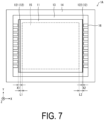
- FIG. 7 is a top view of an electronic element mounting substrate 1A, which is the first variation of the electronic element mounting substrate 1.
- the electronic element mounting substrate 1A illustrated in FIG. 7 is different from the above-described electronic element mounting substrate 1 in that only one combination of the first protrusion portion 121 and the second protrusion portion 122 is provided. Other configurations are the same as those of the electronic element mounting substrate 1. In this case, in a top view, the first protrusion portion 121 and the second protrusion portion 122 are located between the element mounting portion 15 and the electrode pads 16.
- the electronic element mounting substrate 1A having this configuration also achieves the same or similar effects as those of the above-described electronic element mounting substrate 1. Since the electronic element mounting substrate 1A has one set of sides provided with no protrusion portion, the electronic element mounting substrate 1A can be downsized.
- FIG. 8 is a top view of an electronic element mounting substrate 1B, which is the second variation of the electronic element mounting substrate 1.
- the electronic element mounting substrate 1B illustrated in FIG. 8 includes two sets of combinations of the first protrusion portion 121 and the second protrusion portion 122.
- the electronic element mounting substrate 1B is different from the above-described electronic element mounting substrate 1 in that the first protrusion portion 121 and the second protrusion portion 122 which are a pair are adjacent to each other.
- the first protrusion portion 121 and the second protrusion portion 122 which are the pair are arranged in an L shape in a top view.
- Other configurations are the same as those of the electronic element mounting substrate 1.
- a protrusion width X1B of the first protrusion portion 121 is larger than a protrusion width X2B of the second protrusion portion 122.
- a distance L1B between the first protrusion portion 121 and the element mounting portion 15 is smaller than a distance L2B between the second protrusion portion 122 and the element mounting portion 15.
- the electronic element mounting substrate 1B having this configuration also achieves the same or similar effects as those of the above-described electronic element mounting substrate 1.
- a protrusion width X1C of the first protrusion portion 121 is larger than a protrusion width X2C of the second protrusion portion 122.
- a distance L1C between the first protrusion portion 121 and the element mounting portion 15 is smaller than a distance L2C between the second protrusion portion 122 and the element mounting portion 15.
- the one second protrusion portion 122 and the other second protrusion portion 122A may face each other with the element mounting portion 15 interposed therebetween.
- FIG. 10 is a partial cross-sectional view of an electronic element mounting substrate 1D, which is the fourth variation of the electronic element mounting substrate 1.
- the electronic element mounting substrate 1D includes a base 11D, a first frame portion 12D, and a second frame portion 13D.
- An inner side surface 123D of the first frame portion 12D and an inner side surface 133D of the second frame portion 13D are inclined outward with respect to the bottom surface of the base 11D.
- the distance from the bottom surface to the upper surface of each of the frame portions can be increased.
- the possibility can be further reduced of the adhesive used when mounting the element reaching the electrode pads 16 provided on an upper portion of the second frame portion 13D.
- FIG. 11 is a partial cross-sectional view of an electronic element mounting substrate 1E, which is the fifth variation of the electronic element mounting substrate 1.
- the electronic element mounting substrate 1E includes a base 11E, a first frame portion 12E, and a second frame portion 13E.
- An inner side surface 123E of the first frame portion 12E and an inner side surface 133E of the second frame portion 13E are inclined inward with respect to the bottom surface of the base 11D.
- an acute angle can be provided between the inner side surface 123E and the bottom surface of the first frame portion 12E.
- An acute angle can be provided between the inner side surface 133E of the second frame portion 13E and the upper surface of the first frame portion 12E.
Landscapes
- Engineering & Computer Science (AREA)
- Microelectronics & Electronic Packaging (AREA)
- Solid State Image Pick-Up Elements (AREA)
- Structures For Mounting Electric Components On Printed Circuit Boards (AREA)
Abstract
Description
- The present disclosure relates to an electronic element mounting substrate, an electronic device including the electronic element mounting substrate, and an electronic module.
- As an electronic element mounting substrate including a recessed portion inside which an electronic element is accommodated, for example, as disclosed in Patent Document 1 (
JP 2005-203485 A - Patent Document 1:
JP 2005-203485 A - In an aspect of the present disclosure, an electronic element mounting substrate includes a base having a rectangular shape in a plan view and comprising an element mounting portion on which an element is mounted; a first frame portion located on an upper surface of the base; and a second frame portion located on an upper surface of the first frame portion. In the electronic element mounting substrate, the first frame portion comprises at least one set of a first protrusion portion and a second protrusion portion each protruding further than the second frame portion to a side of the element mounting portion, a protrusion width of the first protrusion portion is larger than a protrusion width of the second protrusion portion, and a distance between the first protrusion portion and the element mounting portion is smaller than a distance between the second protrusion portion and the element mounting portion.
- In an aspect of the present disclosure, an electronic device includes the electronic element mounting substrate and an element.
- In an aspect of the present disclosure, an electronic module includes the electronic device and a lid located above the electronic device.
-
-
FIG. 1 is a cross-sectional view of an electronic module according to a first embodiment of the present disclosure. -
FIG. 2 is a cross-sectional view of an electronic device according to the first embodiment of the present disclosure, and is a cross-sectional view taken along the arrow line II-II inFIG. 3 . -
FIG. 3 is a top view of the electronic device according to the first embodiment of the present disclosure. -
FIG. 4 is a cross-sectional view of an electronic element mounting substrate according to the first embodiment of the present disclosure, and is a cross-sectional view taken along the arrow line IV-IV inFIG. 5 . -
FIG. 5 is a top view of the electronic element mounting substrate according to the first embodiment of the present disclosure. -
FIG. 6 is a cross-sectional view of the electronic element mounting substrate according to the first embodiment of the present disclosure, and illustrates an example in which the electronic element mounting substrate includes aninsulating film 17 and aninsulating film 18. -
FIG. 7 is a top view of a first variation of the electronic element mounting substrate. -
FIG. 8 is a top view of a second variation of the electronic element mounting substrate. -
FIG. 9 is a top view of a third variation of the electronic element mounting substrate. -
FIG. 10 is a partial cross-sectional view of a fourth variation of the electronic element mounting substrate. -
FIG. 11 is a partial cross-sectional view of a fifth variation of the electronic element mounting substrate. -
FIG. 12 is a partial cross-sectional view of a sixth variation of the electronic element mounting substrate. - As in the substrate described in
Patent Document 1, a case will be considered in which a plurality of frame portions for forming a recessed portion include opening portions having the same length in a predetermined direction (the frame portions have the same shape). In the case of such a substrate, there has been a concern that the bottom area of the recessed portion, seen from the side of the opening portion when the substrate is viewed in a plan view, is reduced as a result of the position of the opening portion being shifted due to a process error in a layering and pressing process (hereinafter referred to as a layering process). - According to an aspect of the present disclosure, even in a case in which the position shift occurs in the process of layering the plurality of frame portions, the possibility can be reduced of a change in the bottom area of the recessed portion visible from the side of the opening portion when an electronic element mounting substrate is viewed in a plan view.
- Several exemplary embodiments of the present disclosure will be described hereinafter with reference to the drawings. In the following description, a configuration in which an element is mounted on an electronic element mounting substrate will be referred to as an electronic device. A configuration including an element and a lid located on the upper surface side of the element will be referred to as an electronic module. With respect to the electronic element mounting substrate, the electronic device, and the electronic module, any direction may be defined as upward or downward, but for the sake of convenience, the orthogonal coordinate system xyz will be used herein, with a positive direction in a z direction defined as upward.
- In the following embodiment, an example in which an
electronic device 200 includes an element that is animaging element 20 will be described with reference toFIGs. 1 to 6 . -
FIG. 1 is a cross-sectional view of anelectronic module 500 according to the present embodiment. Theelectronic module 500 includes theelectronic device 200 and alid 51 located above theelectronic device 200.FIG. 2 is a cross-sectional view of theelectronic device 200 according to the present embodiment, and is a cross-sectional view taken along the arrow line II-II inFIG. 3 . Theelectronic device 200 includes an electronicelement mounting substrate 1 and theimaging element 20.FIG. 3 is a top view of theelectronic device 200.FIG. 4 is a cross-sectional view of the electronicelement mounting substrate 1 according to the present embodiment, and is a cross-sectional view taken along the arrow line IV-IV inFIG. 5. FIG. 5 is a top view of the electronicelement mounting substrate 1.FIG. 6 is a cross-sectional view of the electronicelement mounting substrate 1 according to the present embodiment, and illustrates an example in which the electronicelement mounting substrate 1 includes aninsulating film 17 and aninsulating film 18. Hereinafter, constituent elements included in theelectronic module 500, theelectronic device 200, and the electronicelement mounting substrate 1 will be described in detail. - The electronic
element mounting substrate 1 is a base for mounting theimaging element 20, and includes abase 11, afirst frame portion 12, asecond frame portion 13, and athird frame portion 14. With this configuration, the electronicelement mounting substrate 1 includes a recessed portion for mounting theimaging element 20.Electrode pads 16 for connection to an element are provided on the upper surface of thesecond frame portion 13. Terminal electrodes (not illustrated) for connection to an external electrical circuit are provided on the lower surface of the electronicelement mounting substrate 1. The terminal electrodes may be provided from the lower surface to the side surface, or on the side surface, instead of being provided on the lower surface of the electronicelement mounting substrate 1. The electronicelement mounting substrate 1 may include an electrode formed between insulation layers, and a through-hole conductor vertically connecting an internal wiring conductor and internal wiring. These electrodes, internal wiring conductors, or through-hole conductors may be exposed at the surface of the electronicelement mounting substrate 1. Theelectrode pads 16 and the terminal electrodes may be electrically connected by the electrodes, the internal wiring conductors, or the through-hole conductors. - The
base 11 has a rectangular shape in a plan view, and includes anelement mounting portion 15 on which theimaging element 20 is mounted. Thebase 11 is constituted by at least oneinsulation layer 110. Thefirst frame portion 12 is located on the upper surface of thebase 11 so as to surround theelement mounting portion 15. In other words, when thefirst frame portion 12 is layered on the upper surface of thebase 11, thefirst frame portion 12 has an opening portion at a position surrounding theelement mounting portion 15. Thefirst frame portion 12 is constituted by at least oneinsulation layer 120. Thesecond frame portion 13 is located on the upper surface of thefirst frame portion 12, and has the upper surface provided with theelectrode pads 16. When thesecond frame portion 13 is layered on the upper surface of thefirst frame portion 12, thesecond frame portion 13 has an opening portion at a position surrounding theelement mounting portion 15. Thesecond frame portion 13 is constituted by at least oneinsulation layer 130. Thethird frame portion 14 is not necessarily a necessary constituent element, and may be provided on the upper surface of thesecond frame portion 13 as necessary. Thethird frame portion 14 may be constituted by aninsulation layer 140 as a constituent element of the electronicelement mounting substrate 1, or may be integrated with thelid 51 as a part of a constituent element of thelid 51 described later. - In the
base 11, theelement mounting portion 15 is a region in which theimaging element 20 is mounted. The component mounted on theelement mounting portion 15 is not limited to the above-describedimaging element 20, and may be at least one of other electronic elements or electronic components. Theelement mounting portion 15 may be, for example, a region overlapping a component to be mounted on theelement mounting portion 15 on the upper surface of thebase 11. Alternatively, theelement mounting portion 15 may be a region located on the upper surface of thebase 11 and surrounded by a virtual line connecting alignment marks used when mounting the component to be mounted on theelement mounting portion 15. Alternatively, theelement mounting portion 15 may be a region in which a metallization layer for mounting is located, the metallization layer being provided between the component mounted on theelement mounting portion 15 and the upper surface of thebase 11. - As illustrated in
FIG. 6 , thebase 11 may include the insulatingfilm 17 at a position overlapping the upper surface of thebase 11 and the inner edge of thefirst frame portion 12. With this configuration, a lower portion of the inner edge of thefirst frame portion 12 is reinforced, and thus, the possibility can be reduced of thefirst frame portion 12 being deformed due to a pressure at the time of performing layering. Although stress is likely to be applied to the base 11 immediately below the inner edge of the first frame portion and the internal wiring inside thebase 11 by the pressure at the time of performing layering, the possibility can be reduced of generation of a crack in the base 11 immediately below the inner edge of the first frame portion or in the internal wiring inside thebase 11. - The
base 11 is constituted by at least one of the insulation layers 110. The surface of theuppermost insulation layer 110 of the at least one of the insulation layers 110 may be exposed. The exposure of the surface of theinsulation layer 110 means that theinsulation layer 110 does not include an alumina coating layer or a metallization layer, and an electrically insulating ceramic or the like included in theinsulation layer 110 is exposed. As illustrated inFIG. 6 , when the insulatingfilm 17 is provided on a part of the surface of thebase 11, the other part thereof may be exposed. That is, at least a part of the surface of theuppermost insulation layer 110 may be exposed. In a related art, a method can be given in which an alumina coat or a metallization layer is provided on a surface on which an element is mounted using an adhesive, as a countermeasure against creeping-up of the adhesive. However, the alumina coating layer or the metallization layer may cause adhesion of dust, adhesion of gold plating, irregular reflection of incident light, or the like. Since the surface of theinsulation layer 110 located at the uppermost layer of thebase 11 is exposed, the possibility of occurrence of a problem such as that described above can be reduced. - In the electronic
element mounting substrate 1, thefirst frame portion 12 is constituted by the plurality ofinsulation layers 120, and inner side surfaces 123 of the plurality ofinsulation layers 120 coincide with each other in a plan view. With this configuration, the flatness of the upper surface of thefirst frame portion 12 can be improved. Thus, the possibility can be reduced of thesecond frame portion 13 being deformed (drooping) at the time of layering thesecond frame portion 13. - As illustrated in
FIG. 6 , thefirst frame portion 12 may include the insulatingfilm 18 at a position overlapping the upper surface of thefirst frame portion 12 and the inner edge of thesecond frame portion 13. With this configuration, a lower portion of the inner edge of thesecond frame portion 13 is reinforced, and thus, the possibility can be reduced of thesecond frame portion 13 being deformed due to the pressure at the time of performing layering. The possibility can be reduced of generation of the crack in thefirst frame portion 12, thebase 11, or the internal wiring immediately below the inner edge of thesecond frame portion 13, to which stress is likely to be applied by the pressure at the time of performing layering. - The
first frame portion 12 includes afirst protrusion portion 121 and asecond protrusion portion 122 each protruding further than thesecond frame portion 13 to the side of theelement mounting portion 15. When the electronicelement mounting substrate 1 is made of an electrically insulating ceramic, the insulation layers each in a state of being a ceramic green sheet are layered and pressed. By including thefirst protrusion portion 121 and thesecond protrusion portion 122, the possibility can be reduced of theinsulation layer 130 drooping when the second frame portion 13 (insulation layer 130) including theelectrode pads 16 is layered. - The electronic
element mounting substrate 1 includes two sets of combinations of thefirst protrusion portion 121 and thesecond protrusion portion 122. For the sake of convenience, the first pair will be referred to as thefirst protrusion portion 121 and thesecond protrusion portion 122, and the second pair will be referred to as afirst protrusion portion 121A and asecond protrusion portion 122A. As illustrated inFIG. 5 , in the electronicelement mounting substrate 1, thefirst protrusion portion 121 and thesecond protrusion portion 122 which are the pair face each other with theelement mounting portion 15 interposed therebetween. In the electronicelement mounting substrate 1, a protrusion width X1 of thefirst protrusion portion 121 is larger than a protrusion width X2 of thesecond protrusion portion 122. A distance L1 between thefirst protrusion portion 121 and theelement mounting portion 15 is smaller than a distance L2 between thesecond protrusion portion 122 and theelement mounting portion 15. Each of the protrusion widths X1 and X2 indicates, for example, the width of the upper surface of thefirst frame portion 12 protruding from the lower surface of thesecond frame portion 13. Each of the distances L1 and L2 indicates the distance between the outer edge of the upper surface of thefirst frame portion 12 on theelement mounting portion 15 side and the outer edge of theelement mounting portion 15 in a top view. These also apply to when the side surface of thefirst frame portion 12 and/or thesecond frame portion 13 on theelement mounting portion 15 side is inclined with respect to the bottom surface of thebase 11. - A protrusion width X1A of the
first protrusion portion 121A is larger than a protrusion width X2A of thesecond protrusion portion 122A. A distance L1A between thefirst protrusion portion 121A and theelement mounting portion 15 is smaller than a distance L2A between thesecond protrusion portion 122A and theelement mounting portion 15. The protrusion width X1 and the protrusion width X1A may have the same length or may have different lengths. The protrusion width X2 and the protrusion width X2A may also have the same length or may have different lengths. The distance L1 and the distance L1A may have the same length or may have different lengths. The distance L2 and the distance L2A may also have the same length or may have different lengths. - With this configuration, even if a position shift occurs in the layering process of the
first frame portion 12 and thesecond frame portion 13, the possibility can be reduced of a change in the bottom area of the recessed portion visible when the electronicelement mounting substrate 1 is viewed from the upper surface thereof. The bottom surface of the recessed portion visible when the electronicelement mounting substrate 1 is viewed from the upper surface thereof is a surface region defined by the upper surface of thebase 11 and the inner edges of thefirst frame portion 12 and thesecond frame portion 13 when the electronicelement mounting substrate 1 is viewed from above. The bottom surface of the recessed portion includes theelement mounting portion 15, and when the bottom area of the recessed portion is reduced, a problem may occur when an element is mounted. Thus, the fact that the size of the bottom area of the recessed portion does not change is a significant effect in terms of the electronic element mounting substrate. - The
imaging element 20 may be disposed on the upper surface of the base 11 with an adhesive interposed therebetween. Examples of the adhesive include a silver epoxy and a thermosetting resin. When theimaging element 20 is mounted using the adhesive, the adhesive is pushed out in some cases. The distance L1 between thefirst protrusion portion 121 and theelement mounting portion 15 is smaller than the distance L2 between thesecond protrusion portion 122 and theelement mounting portion 15. However, since the width X1 of thefirst protrusion portion 121 is wider than the width X2 of thesecond protrusion portion 122, the pushed-out adhesive can spread horizontally on the upper surface of thefirst protrusion portion 121. The width X2 of thesecond protrusion portion 122 is narrower than the width X1 of thefirst protrusion portion 121. However, since the distance L2 between thesecond protrusion portion 122 and theelement mounting portion 15 is larger than the distance L1 between thefirst protrusion portion 121 and theelement mounting portion 15, the pushed-out adhesive can spread horizontally on the upper surface of thebase 11. Thus, the possibility of the pushed-out adhesive reaching theelectrode pads 16 can be reduced. Therefore, in theelectronic device 200 and theelectronic module 500 each including the electronicelement mounting substrate 1, the possibility of deterioration of the electrical characteristics can be reduced. - Since the electronic
element mounting substrate 1 has a rectangular shape and the opening portion of thefirst frame portion 12 also has a rectangular shape, it can be said that the protrusion width X1 is the distance between the short side of the opening portion of thefirst frame portion 12 and the element mounting portion. It can be also said that the protrusion width X1A is the distance between the long side of the opening portion of thefirst frame portion 12 and the element mounting portion. In the electronicelement mounting substrate 1, the distance between the short side of the opening portion of thefirst frame portion 12 and theelement mounting portion 15 may be larger than the distance between the long side of the opening portion and theelement mounting portion 15. With this configuration, by increasing the distance between the inner edge of the frame portion and the element mounting portion on the side of the short side on which the adhesive is more likely to creep up, the possibility can be further reduced of the adhesive reaching the electrode pads provided on an upper portion of the second frame portion. - In the electronic
element mounting substrate 1, when a direction (z direction) perpendicular to the upper surface of thebase 11 is a thickness direction, the thickness of thefirst frame portion 12 may be larger than the thickness of thesecond frame portion 13. Alternatively, the number of the insulation layers 110 of thefirst frame portion 12 may be greater than the number of the insulation layers 130 of thesecond frame portion 13. With this configuration, the strength of the electronicelement mounting substrate 1 is improved. The possibility is further reduced of the adhesive reaching theelectrode pads 16 provided on the upper portion of the second frame portion. - The
imaging element 20 may be, for example, an imaging element of a complementary metal oxide semiconductor (CCD) type, a complementary metal oxide semiconductor (CMOS) type, or the like. Although an example in which theelectronic device 200 includes theimaging element 20 is described in the present embodiment, the element according to the present disclosure is not limited to the imaging element. The element according to the present disclosure may be a light-emitting element such as a light-emitting diode (LED) or a laser diode (LD), an element having a sensor function of sensing pressure, air pressure, acceleration, gyro, or the like, an integrated circuit, or the like in addition to theimaging element 20. Theimaging element 20 and the electronicelement mounting substrate 1 may be electrically connected to each other by, for example, connectingmembers 22 such as wire bonding members. - Given the characteristics of the
imaging element 20, it may include aheat generating portion 21. Theheat generating portion 21 is a portion that is more likely to generate heat than other portions, and is, for example, a calculation unit. As illustrated inFIGs. 2 and3 , normally, theheat generating portion 21 can be present at a position displaced to one side from the center of the element. In the present embodiment, theheat generating portion 21 is located closer to thesecond protrusion portion 122 than to thefirst protrusion portion 121. With this configuration, in theelectronic device 200 and theelectronic module 500, the distance between the heat generating portion and the internal wiring present inside thefirst frame portion 12 and thesecond frame portion 13 can be increased. Thus, a resistance change due to heat can be reduced, and the electrical characteristics of theelectronic device 200 and theelectronic module 500 can be improved. - When the element to be mounted on
electronic device 200 is the imaging element such as a CCD or a CMOS, or the light-emitting element such as an LED or an LD, a member having high transparency such as a glass material is used for thelid 51. Thelid 51 may include a lens holder and a lens made of a resin, liquid, glass, crystal, or the like. When the element to be mounted on theelectronic device 200 is the integrated circuit or the like, a metal material, a ceramic material, or an organic material may be used as the material for thelid 51. Thelid 51 may be bonded to the electronicelement mounting substrate 1 using a lid bonding material. As the lid bonding material, a thermosetting resin, low-melting point glass, or a brazing material containing a metal component may be used, for example. - In the electronic
element mounting substrate 1, the material of the insulation layers 110, 120, 130, and 140 included in the electronicelement mounting substrate 1 includes, for example, an electrically insulating ceramic or a resin. As the electrically insulating ceramic, for example, a ceramic such as an aluminum oxide sintered body (alumina ceramic), an aluminum nitride sintered body, a silicon nitride sintered body, a mullite sintered body, or a glass ceramic sintered body can be used. Examples of the resin include an epoxy resin, a polyimide resin, an acrylic resin, a phenol resin, and a fluorine-based resin. Examples of the fluorine-based resin include a polyester resin and a tetrafluoroethylene resin. - When the electronic
element mounting substrate 1 is, for example, an aluminum oxide sintered body, a slurry is produced by adding a suitable organic binder, solvent, and the like to a raw material powder of aluminum oxide (Al2O3), silicon oxide (SiO2), magnesium oxide (MgO), calcium oxide (CaO), or the like, and then mixing them. A ceramic green sheet is produced by forming this slurry into a sheet by employing a well-known doctor blade method, calender roll method, or the like. This ceramic green sheet is subjected to an appropriate punching process, and multiple ceramic green sheets are layered to form a green body, which is then fired at a high temperature (approximately 1600°C) to produce the electronicelement mounting substrate 1. - The
electrode pads 16 and the terminal electrodes mainly contain, for example, metals such as tungsten, molybdenum, manganese, copper, silver, palladium, gold, platinum, nickel, or cobalt, or alloys containing any of these metals as conductor materials. Theelectrode pads 16 and the terminal electrodes are formed on the surfaces of the electronicelement mounting substrate 1 as metal layers such as metallization layers or plating layers of a conductor material. The internal wiring conductor is formed inside the electronicelement mounting substrate 1 by metallization of a conductor material. - When the
electrode pads 16, the internal wiring conductors, and the terminal electrodes are, for example, metallization layers of tungsten, they can be formed by printing a metal paste prepared by mixing tungsten powder with an organic solvent and an organic binder at predetermined positions on the ceramic green sheets to be the electronicelement mounting substrate 1 by a screen printing method or the like and firing the paste. A plating layer of nickel, gold, or the like may be further deposited on exposed surfaces of the metallization layers, which serve as the internal wiring conductors and the terminal electrodes, by an electrolytic plating method, an electroless plating method, or the like. - Hereinafter, a first variation of the electronic
element mounting substrate 1 will be described with reference toFIG. 7 . For the sake of convenience of description, members having the same functions as those of the members described in the above-described embodiment are denoted by the same reference signs, and description thereof is not repeated. The same applies to other variations.FIG. 7 is a top view of an electronicelement mounting substrate 1A, which is the first variation of the electronicelement mounting substrate 1. - The electronic
element mounting substrate 1A illustrated inFIG. 7 is different from the above-described electronicelement mounting substrate 1 in that only one combination of thefirst protrusion portion 121 and thesecond protrusion portion 122 is provided. Other configurations are the same as those of the electronicelement mounting substrate 1. In this case, in a top view, thefirst protrusion portion 121 and thesecond protrusion portion 122 are located between theelement mounting portion 15 and theelectrode pads 16. - The electronic
element mounting substrate 1A having this configuration also achieves the same or similar effects as those of the above-described electronicelement mounting substrate 1. Since the electronicelement mounting substrate 1A has one set of sides provided with no protrusion portion, the electronicelement mounting substrate 1A can be downsized. - A second variation of the electronic
element mounting substrate 1 will be described with reference toFIG. 8. FIG. 8 is a top view of an electronicelement mounting substrate 1B, which is the second variation of the electronicelement mounting substrate 1. - The electronic
element mounting substrate 1B illustrated inFIG. 8 includes two sets of combinations of thefirst protrusion portion 121 and thesecond protrusion portion 122. The electronicelement mounting substrate 1B is different from the above-described electronicelement mounting substrate 1 in that thefirst protrusion portion 121 and thesecond protrusion portion 122 which are a pair are adjacent to each other. In other words, in the electronicelement mounting substrate 1B, thefirst protrusion portion 121 and thesecond protrusion portion 122 which are the pair are arranged in an L shape in a top view. Other configurations are the same as those of the electronicelement mounting substrate 1. - In the electronic
element mounting substrate 1B, a protrusion width X1B of thefirst protrusion portion 121 is larger than a protrusion width X2B of thesecond protrusion portion 122. A distance L1B between thefirst protrusion portion 121 and theelement mounting portion 15 is smaller than a distance L2B between thesecond protrusion portion 122 and theelement mounting portion 15. - The electronic
element mounting substrate 1B having this configuration also achieves the same or similar effects as those of the above-described electronicelement mounting substrate 1. - A third variation of the electronic
element mounting substrate 1 will be described with reference toFIG. 9. FIG. 9 is a top view of an electronicelement mounting substrate 1C, which is the third variation of the electronicelement mounting substrate 1. - The electronic
element mounting substrate 1C illustrated inFIG. 9 includes two sets of combinations of thefirst protrusion portion 121 and thesecond protrusion portion 122. The electronicelement mounting substrate 1C is different from the electronicelement mounting substrate 1 in that the onefirst protrusion portion 121 and the otherfirst protrusion portion 121A face each other with theelement mounting portion 15 interposed therebetween. In the electronicelement mounting substrate 1C, thefirst protrusion portion 121 and thesecond protrusion portion 122 which are a pair are adjacent to each other. In other words, in the electronicelement mounting substrate 1B, thefirst protrusion portion 121 and thesecond protrusion portion 122 which are the pair are arranged in an L shape in a top view. - In the electronic
element mounting substrate 1C, in each of the pairs, a protrusion width X1C of thefirst protrusion portion 121 is larger than a protrusion width X2C of thesecond protrusion portion 122. A distance L1C between thefirst protrusion portion 121 and theelement mounting portion 15 is smaller than a distance L2C between thesecond protrusion portion 122 and theelement mounting portion 15. - In the electronic
element mounting substrate 1C, both of the twosecond protrusion portions element mounting portion 15 and theelectrode pads 16 in a top view. Since widths X1 and X1A of thefirst protrusion portions second protrusion portions first protrusion portions electrode pads 16 can be further reduced. - In another aspect of the electronic
element mounting substrate 1C, the onesecond protrusion portion 122 and the othersecond protrusion portion 122A may face each other with theelement mounting portion 15 interposed therebetween. - In this case, since a distance L2 between the
second protrusion portion 122 and theelement mounting portion 15 is larger than a distance L1 between thefirst protrusion portion 121 and theelement mounting portion 15, the pushed-out adhesive can spread horizontally on the upper surface of thebase 11. Thus, the possibility of the pushed-out adhesive reaching theelectrode pads 16 can be further reduced. - A fourth variation of the electronic
element mounting substrate 1 will be described with reference toFIG. 10. FIG. 10 is a partial cross-sectional view of an electronic element mounting substrate 1D, which is the fourth variation of the electronicelement mounting substrate 1. - As illustrated in
FIG. 10 , the electronic element mounting substrate 1D includes abase 11D, afirst frame portion 12D, and asecond frame portion 13D. Aninner side surface 123D of thefirst frame portion 12D and aninner side surface 133D of thesecond frame portion 13D are inclined outward with respect to the bottom surface of thebase 11D. - With this configuration, at the
inner side surface 123D of thefirst frame portion 12D and theinner side surface 133D of thesecond frame portion 13D, the distance from the bottom surface to the upper surface of each of the frame portions can be increased. Thus, the possibility can be further reduced of the adhesive used when mounting the element reaching theelectrode pads 16 provided on an upper portion of thesecond frame portion 13D. - A fifth variation of the electronic
element mounting substrate 1 will be described with reference toFIG. 11. FIG. 11 is a partial cross-sectional view of an electronicelement mounting substrate 1E, which is the fifth variation of the electronicelement mounting substrate 1. - As illustrated in
FIG. 11 , the electronicelement mounting substrate 1E includes abase 11E, afirst frame portion 12E, and asecond frame portion 13E. Aninner side surface 123E of thefirst frame portion 12E and aninner side surface 133E of thesecond frame portion 13E are inclined inward with respect to the bottom surface of thebase 11D. - With this configuration, an acute angle can be provided between the
inner side surface 123E and the bottom surface of thefirst frame portion 12E. An acute angle can be provided between theinner side surface 133E of thesecond frame portion 13E and the upper surface of thefirst frame portion 12E. Thus, the adhesive used when mounting the element is trapped by acute angle portions, and further, since each of the inner side surfaces is inclined inward, creeping-up of the adhesive can be suppressed. Thus, the possibility can be further reduced of the adhesive reaching theelectrode pads 16 provided on an upper portion of thesecond frame portion 13E. - A sixth variation of the electronic
element mounting substrate 1 will be described with reference toFIG. 12. FIG. 12 is a partial cross-sectional view of an electronicelement mounting substrate 1F, which is the sixth variation of the electronicelement mounting substrate 1. - As illustrated in
FIG. 12 , the electronicelement mounting substrate 1F includes abase 11F, afirst frame portion 12F, and asecond frame portion 13F. When a direction (z direction) perpendicular to the upper surface of thebase 11F is defined as a thickness direction, the thickness of aninner side surface 123F of thefirst frame portion 12F is thicker than an outer side surface 124F of thefirst frame portion 12F. - With this configuration, the possibility can be further reduced of the adhesive used when mounting the element reaching the
electrode pads 16 provided on an upper portion of thesecond frame portion 13F. - In the present disclosure, the invention has been described above based on the various drawings and examples. However, the invention according to the present disclosure is not limited to each embodiment described above. That is, the invention according to the present disclosure can be modified in various ways within the scope illustrated in the present disclosure, and embodiments obtained by appropriately combining the technical means disclosed in different embodiments are also included in the technical scope of the invention according to the present disclosure. In other words, a person skilled in the art can easily make various variations or modifications based on the present disclosure. Note that these variations or modifications are included within the scope of the present disclosure.
-
- 1, 1A, 1B, 1C, 1D, 1E, 1F Electronic element mounting substrate
- 11, 11D, 11E, 11F Base
- 12, 12D, 12E, 12F First frame portion
- 121, 121A First protrusion portion
- 13, 13D, 13E, 13F Second frame portion
- 122, 122A Second protrusion portion
- 14 Third frame portion
- 15 Element mounting portion
- 16 Electrode pad
- 17, 18 Insulating film
- 20 Imaging element (element)
- 21 Heat generating portion
- 22 Connecting member
- 51 Lid
- 110, 120, 130, 140 Insulation layer
- 200 Electronic device
- 500 Electronic module
Claims (12)
- An electronic element mounting substrate comprising:a base having a rectangular shape in a plan view and comprising an element mounting portion on which an element is mounted;a first frame portion located on an upper surface of the base; anda second frame portion located on an upper surface of the first frame portion, whereinthe first frame portion comprises at least one set of a first protrusion portion and a second protrusion portion each protruding further than the second frame portion to a side of the element mounting portion,a protrusion width of the first protrusion portion is larger than a protrusion width of the second protrusion portion, anda distance between the first protrusion portion and the element mounting portion is smaller than a distance between the second protrusion portion and the element mounting portion.
- The electronic element mounting substrate according to claim 1, whereinthe base is constituted by at least one insulation layer, anda surface of the insulation layer located at an uppermost layer is exposed.
- The electronic element mounting substrate according to claim 1 or 2, whereina direction perpendicular to the upper surface of the base is a thickness direction, anda thickness of the first frame portion is larger than a thickness of the second frame portion.
- The electronic element mounting substrate according to any one of claims 1 to 3, wherein
the first frame portion is constituted by a plurality of insulation layers, and inner side surfaces of the plurality of insulation layers coincide with each other in a plan view. - The electronic element mounting substrate according to any one of claims 1 to 4, wherein
the base comprises an insulating film at a position at which the upper surface of the base and an inner edge of the first frame portion overlap with each other. - The electronic element mounting substrate according to any one of claims 1 to 5, wherein
the first frame portion comprises an insulating film at a position at which the upper surface of the first frame portion and an inner edge of the second frame portion overlap with each other. - The electronic element mounting substrate according to any one of claims 1 to 3, wherein
at least one of an inner side surface of the first frame portion or an inner side surface of the second frame portion is inclined with respect to a bottom surface of the base. - The electronic element mounting substrate according to any one of claims 1 to 7, whereina direction perpendicular to the upper surface of the base is a thickness direction, anda thickness of an inner side surface of the first frame portion is larger than a thickness of an outer side surface of the first frame portion.
- The electronic element mounting substrate according to any one of claims 1 to 8, wherein
a shape of an opening portion of the first frame portion is a rectangular shape, and a distance between a short side of the opening portion and the element mounting portion is larger than a distance between a long side of the opening portion and the element mounting portion. - An electronic device comprising:the electronic element mounting substrate according to any one of claims 1 to 9; andan element.
- The electronic device according to claim 10, whereinthe element comprises a heat generating portion, andthe heat generating portion is located at a position closer to the second protrusion portion than to the first protrusion portion.
- An electronic module comprising:the electronic device according to claim 10 or 11; anda lid located above the electronic device.
Applications Claiming Priority (2)
| Application Number | Priority Date | Filing Date | Title |
|---|---|---|---|
| JP2021139371 | 2021-08-27 | ||
| PCT/JP2022/030999 WO2023026904A1 (en) | 2021-08-27 | 2022-08-17 | Substrate for mounting electronic element, electronic device, and electronic module |
Publications (1)
| Publication Number | Publication Date |
|---|---|
| EP4395473A1 true EP4395473A1 (en) | 2024-07-03 |
Family
ID=85321978
Family Applications (1)
| Application Number | Title | Priority Date | Filing Date |
|---|---|---|---|
| EP22861192.7A Withdrawn EP4395473A1 (en) | 2021-08-27 | 2022-08-17 | Substrate for mounting electronic element, electronic device, and electronic module |
Country Status (6)
| Country | Link |
|---|---|
| US (1) | US20240355845A1 (en) |
| EP (1) | EP4395473A1 (en) |
| JP (1) | JP7652908B2 (en) |
| KR (1) | KR20240037326A (en) |
| CN (1) | CN117837275A (en) |
| WO (1) | WO2023026904A1 (en) |
Family Cites Families (10)
| Publication number | Priority date | Publication date | Assignee | Title |
|---|---|---|---|---|
| JPS63182570U (en) * | 1987-05-19 | 1988-11-24 | ||
| JP3470852B2 (en) * | 1996-12-25 | 2003-11-25 | 日本特殊陶業株式会社 | Wiring board and its manufacturing method |
| JP2005203485A (en) | 2004-01-14 | 2005-07-28 | Ngk Spark Plug Co Ltd | Electronic component storage container |
| JP2013120867A (en) | 2011-12-08 | 2013-06-17 | Seiko Epson Corp | Package, electronic device and electronic apparatus |
| CN105210183B (en) | 2014-04-23 | 2018-06-12 | 京瓷株式会社 | Electronic component mounting substrate and electronic device |
| JP6677595B2 (en) | 2016-07-11 | 2020-04-08 | 京セラ株式会社 | Electronic element mounting substrate, electronic device, and electronic module |
| JP2018019214A (en) | 2016-07-27 | 2018-02-01 | 京セラ株式会社 | Crystal oscillator |
| JP6818581B2 (en) | 2017-02-20 | 2021-01-20 | 京セラ株式会社 | Electronic component storage packages, electronic devices and electronic modules |
| JP6955366B2 (en) | 2017-04-25 | 2021-10-27 | 京セラ株式会社 | Substrate for mounting electronic devices, electronic devices and electronic modules |
| JP6625774B1 (en) | 2019-02-20 | 2019-12-25 | 中央電子工業株式会社 | Hollow package structure and its manufacturing method, and semiconductor device and its manufacturing method |
-
2022
- 2022-08-17 JP JP2023543830A patent/JP7652908B2/en active Active
- 2022-08-17 CN CN202280057383.9A patent/CN117837275A/en active Pending
- 2022-08-17 US US18/686,337 patent/US20240355845A1/en active Pending
- 2022-08-17 WO PCT/JP2022/030999 patent/WO2023026904A1/en not_active Ceased
- 2022-08-17 EP EP22861192.7A patent/EP4395473A1/en not_active Withdrawn
- 2022-08-17 KR KR1020247006217A patent/KR20240037326A/en not_active Ceased
Also Published As
| Publication number | Publication date |
|---|---|
| KR20240037326A (en) | 2024-03-21 |
| JPWO2023026904A1 (en) | 2023-03-02 |
| US20240355845A1 (en) | 2024-10-24 |
| WO2023026904A1 (en) | 2023-03-02 |
| CN117837275A (en) | 2024-04-05 |
| JP7652908B2 (en) | 2025-03-27 |
Similar Documents
| Publication | Publication Date | Title |
|---|---|---|
| CN104335345B (en) | Wiring substrate and electronic device | |
| US10334740B2 (en) | Electronic-component mount substrate, electronic device, and electronic module | |
| JP6140834B2 (en) | Wiring board and electronic device | |
| CN104412722B (en) | Circuit board, electronic device and light-emitting device | |
| US10985098B2 (en) | Electronic component mounting substrate, electronic device, and electronic module | |
| EP4395473A1 (en) | Substrate for mounting electronic element, electronic device, and electronic module | |
| US10319672B2 (en) | Wiring board, electronic device, and electronic module | |
| JP2021184481A (en) | Electronic module | |
| JP6626735B2 (en) | Electronic component mounting board, electronic device and electronic module | |
| JP6780996B2 (en) | Wiring boards, electronics and electronic modules | |
| JPWO2023026904A5 (en) | ||
| CN110291628B (en) | Wiring substrate, electronic device and electronic module | |
| CN110326101B (en) | Wiring substrates, electronic devices and electronic modules | |
| CN107431047B (en) | Wiring substrate, electronic device, and electronic module | |
| JP6818609B2 (en) | Wiring substrate and imaging device | |
| JP6737646B2 (en) | Wiring board, electronic device and electronic module | |
| US20250233059A1 (en) | Electronic element mounting substrate, electronic device, electronic module, and method for manufacturing electronic element mounting substrate | |
| JP6514036B2 (en) | Electronic component mounting substrate, electronic device and electronic module |
Legal Events
| Date | Code | Title | Description |
|---|---|---|---|
| STAA | Information on the status of an ep patent application or granted ep patent |
Free format text: STATUS: THE INTERNATIONAL PUBLICATION HAS BEEN MADE |
|
| PUAI | Public reference made under article 153(3) epc to a published international application that has entered the european phase |
Free format text: ORIGINAL CODE: 0009012 |
|
| STAA | Information on the status of an ep patent application or granted ep patent |
Free format text: STATUS: REQUEST FOR EXAMINATION WAS MADE |
|
| 17P | Request for examination filed |
Effective date: 20240222 |
|
| AK | Designated contracting states |
Kind code of ref document: A1 Designated state(s): AL AT BE BG CH CY CZ DE DK EE ES FI FR GB GR HR HU IE IS IT LI LT LU LV MC MK MT NL NO PL PT RO RS SE SI SK SM TR |
|
| DAV | Request for validation of the european patent (deleted) | ||
| DAX | Request for extension of the european patent (deleted) | ||
| STAA | Information on the status of an ep patent application or granted ep patent |
Free format text: STATUS: THE APPLICATION HAS BEEN WITHDRAWN |
|
| 18W | Application withdrawn |
Effective date: 20250527 |