EP4395360A1 - Imaging device and electronic apparatus - Google Patents
Imaging device and electronic apparatus Download PDFInfo
- Publication number
- EP4395360A1 EP4395360A1 EP22861201.6A EP22861201A EP4395360A1 EP 4395360 A1 EP4395360 A1 EP 4395360A1 EP 22861201 A EP22861201 A EP 22861201A EP 4395360 A1 EP4395360 A1 EP 4395360A1
- Authority
- EP
- European Patent Office
- Prior art keywords
- wall portion
- wall
- imaging device
- pixels
- shaped structure
- Prior art date
- Legal status (The legal status is an assumption and is not a legal conclusion. Google has not performed a legal analysis and makes no representation as to the accuracy of the status listed.)
- Pending
Links
- 238000003384 imaging method Methods 0.000 title claims abstract description 155
- 238000006243 chemical reaction Methods 0.000 claims abstract description 77
- 239000011159 matrix material Substances 0.000 claims abstract description 26
- 239000011800 void material Substances 0.000 claims description 157
- VYPSYNLAJGMNEJ-UHFFFAOYSA-N Silicium dioxide Chemical compound O=[Si]=O VYPSYNLAJGMNEJ-UHFFFAOYSA-N 0.000 claims description 60
- 239000011810 insulating material Substances 0.000 claims description 60
- 238000005192 partition Methods 0.000 claims description 56
- 229910052814 silicon oxide Inorganic materials 0.000 claims description 55
- 238000005530 etching Methods 0.000 claims description 29
- 229910020175 SiOH Inorganic materials 0.000 claims description 3
- 229910052681 coesite Inorganic materials 0.000 claims description 3
- 229910052906 cristobalite Inorganic materials 0.000 claims description 3
- 239000000377 silicon dioxide Substances 0.000 claims description 3
- 229910052682 stishovite Inorganic materials 0.000 claims description 3
- 229910052905 tridymite Inorganic materials 0.000 claims description 3
- 230000002542 deteriorative effect Effects 0.000 abstract description 6
- 230000035945 sensitivity Effects 0.000 abstract description 5
- 230000006872 improvement Effects 0.000 abstract description 2
- 238000010586 diagram Methods 0.000 description 161
- 238000004519 manufacturing process Methods 0.000 description 97
- 239000010410 layer Substances 0.000 description 88
- 230000004048 modification Effects 0.000 description 83
- 238000012986 modification Methods 0.000 description 83
- 229910052581 Si3N4 Inorganic materials 0.000 description 44
- HQVNEWCFYHHQES-UHFFFAOYSA-N silicon nitride Chemical compound N12[Si]34N5[Si]62N3[Si]51N64 HQVNEWCFYHHQES-UHFFFAOYSA-N 0.000 description 44
- 238000000034 method Methods 0.000 description 33
- 238000012545 processing Methods 0.000 description 30
- 239000011347 resin Substances 0.000 description 23
- 229920005989 resin Polymers 0.000 description 23
- 239000000463 material Substances 0.000 description 20
- XUIMIQQOPSSXEZ-UHFFFAOYSA-N Silicon Chemical compound [Si] XUIMIQQOPSSXEZ-UHFFFAOYSA-N 0.000 description 19
- 239000004065 semiconductor Substances 0.000 description 19
- 229910052710 silicon Inorganic materials 0.000 description 19
- 239000010703 silicon Substances 0.000 description 19
- WGTYBPLFGIVFAS-UHFFFAOYSA-M tetramethylammonium hydroxide Chemical compound [OH-].C[N+](C)(C)C WGTYBPLFGIVFAS-UHFFFAOYSA-M 0.000 description 16
- 238000001312 dry etching Methods 0.000 description 15
- 238000001039 wet etching Methods 0.000 description 15
- 229910021417 amorphous silicon Inorganic materials 0.000 description 14
- 230000009467 reduction Effects 0.000 description 14
- NBIIXXVUZAFLBC-UHFFFAOYSA-N Phosphoric acid Chemical compound OP(O)(O)=O NBIIXXVUZAFLBC-UHFFFAOYSA-N 0.000 description 12
- 238000005229 chemical vapour deposition Methods 0.000 description 12
- 238000000926 separation method Methods 0.000 description 12
- NRTOMJZYCJJWKI-UHFFFAOYSA-N Titanium nitride Chemical compound [Ti]#N NRTOMJZYCJJWKI-UHFFFAOYSA-N 0.000 description 11
- 230000006870 function Effects 0.000 description 11
- 239000010936 titanium Substances 0.000 description 11
- 229910016570 AlCu Inorganic materials 0.000 description 10
- 238000005516 engineering process Methods 0.000 description 9
- 239000011368 organic material Substances 0.000 description 9
- 230000000694 effects Effects 0.000 description 8
- 238000000206 photolithography Methods 0.000 description 8
- 239000000243 solution Substances 0.000 description 8
- 230000003287 optical effect Effects 0.000 description 7
- 239000000049 pigment Substances 0.000 description 7
- 238000003860 storage Methods 0.000 description 7
- MZLGASXMSKOWSE-UHFFFAOYSA-N tantalum nitride Chemical compound [Ta]#N MZLGASXMSKOWSE-UHFFFAOYSA-N 0.000 description 7
- MHAJPDPJQMAIIY-UHFFFAOYSA-N Hydrogen peroxide Chemical compound OO MHAJPDPJQMAIIY-UHFFFAOYSA-N 0.000 description 6
- 229910000147 aluminium phosphate Inorganic materials 0.000 description 6
- 239000010949 copper Substances 0.000 description 6
- 238000012937 correction Methods 0.000 description 6
- 238000005520 cutting process Methods 0.000 description 6
- QOSATHPSBFQAML-UHFFFAOYSA-N hydrogen peroxide;hydrate Chemical compound O.OO QOSATHPSBFQAML-UHFFFAOYSA-N 0.000 description 6
- 239000011259 mixed solution Substances 0.000 description 6
- XLYOFNOQVPJJNP-UHFFFAOYSA-N water Substances O XLYOFNOQVPJJNP-UHFFFAOYSA-N 0.000 description 6
- RYGMFSIKBFXOCR-UHFFFAOYSA-N Copper Chemical compound [Cu] RYGMFSIKBFXOCR-UHFFFAOYSA-N 0.000 description 5
- RTAQQCXQSZGOHL-UHFFFAOYSA-N Titanium Chemical compound [Ti] RTAQQCXQSZGOHL-UHFFFAOYSA-N 0.000 description 5
- 229910052782 aluminium Inorganic materials 0.000 description 5
- XAGFODPZIPBFFR-UHFFFAOYSA-N aluminium Chemical compound [Al] XAGFODPZIPBFFR-UHFFFAOYSA-N 0.000 description 5
- 230000015572 biosynthetic process Effects 0.000 description 5
- 229910052802 copper Inorganic materials 0.000 description 5
- 239000002356 single layer Substances 0.000 description 5
- 229910052715 tantalum Inorganic materials 0.000 description 5
- GUVRBAGPIYLISA-UHFFFAOYSA-N tantalum atom Chemical compound [Ta] GUVRBAGPIYLISA-UHFFFAOYSA-N 0.000 description 5
- 229910052719 titanium Inorganic materials 0.000 description 5
- 238000000231 atomic layer deposition Methods 0.000 description 4
- 238000010030 laminating Methods 0.000 description 4
- 230000007246 mechanism Effects 0.000 description 4
- 230000008569 process Effects 0.000 description 4
- 239000000126 substance Substances 0.000 description 4
- 101710141544 Allatotropin-related peptide Proteins 0.000 description 3
- 230000003321 amplification Effects 0.000 description 3
- 238000010560 atom transfer radical polymerization reaction Methods 0.000 description 3
- 230000007423 decrease Effects 0.000 description 3
- 238000003199 nucleic acid amplification method Methods 0.000 description 3
- 238000012546 transfer Methods 0.000 description 3
- PPBRXRYQALVLMV-UHFFFAOYSA-N Styrene Chemical compound C=CC1=CC=CC=C1 PPBRXRYQALVLMV-UHFFFAOYSA-N 0.000 description 2
- 230000008859 change Effects 0.000 description 2
- 230000000295 complement effect Effects 0.000 description 2
- 238000000151 deposition Methods 0.000 description 2
- 238000001514 detection method Methods 0.000 description 2
- 239000003989 dielectric material Substances 0.000 description 2
- NBBQQQJUOYRZCA-UHFFFAOYSA-N diethoxymethylsilane Chemical compound CCOC([SiH3])OCC NBBQQQJUOYRZCA-UHFFFAOYSA-N 0.000 description 2
- 238000009792 diffusion process Methods 0.000 description 2
- 238000005401 electroluminescence Methods 0.000 description 2
- 238000007667 floating Methods 0.000 description 2
- 239000007789 gas Substances 0.000 description 2
- 238000009434 installation Methods 0.000 description 2
- 239000000395 magnesium oxide Substances 0.000 description 2
- CPLXHLVBOLITMK-UHFFFAOYSA-N magnesium oxide Inorganic materials [Mg]=O CPLXHLVBOLITMK-UHFFFAOYSA-N 0.000 description 2
- AXZKOIWUVFPNLO-UHFFFAOYSA-N magnesium;oxygen(2-) Chemical compound [O-2].[Mg+2] AXZKOIWUVFPNLO-UHFFFAOYSA-N 0.000 description 2
- 239000007769 metal material Substances 0.000 description 2
- 229910003465 moissanite Inorganic materials 0.000 description 2
- TWNQGVIAIRXVLR-UHFFFAOYSA-N oxo(oxoalumanyloxy)alumane Chemical compound O=[Al]O[Al]=O TWNQGVIAIRXVLR-UHFFFAOYSA-N 0.000 description 2
- SIWVEOZUMHYXCS-UHFFFAOYSA-N oxo(oxoyttriooxy)yttrium Chemical compound O=[Y]O[Y]=O SIWVEOZUMHYXCS-UHFFFAOYSA-N 0.000 description 2
- BPUBBGLMJRNUCC-UHFFFAOYSA-N oxygen(2-);tantalum(5+) Chemical compound [O-2].[O-2].[O-2].[O-2].[O-2].[Ta+5].[Ta+5] BPUBBGLMJRNUCC-UHFFFAOYSA-N 0.000 description 2
- RVTZCBVAJQQJTK-UHFFFAOYSA-N oxygen(2-);zirconium(4+) Chemical compound [O-2].[O-2].[Zr+4] RVTZCBVAJQQJTK-UHFFFAOYSA-N 0.000 description 2
- 229920002120 photoresistant polymer Polymers 0.000 description 2
- 238000005268 plasma chemical vapour deposition Methods 0.000 description 2
- 239000002243 precursor Substances 0.000 description 2
- 210000001747 pupil Anatomy 0.000 description 2
- 230000002441 reversible effect Effects 0.000 description 2
- HBMJWWWQQXIZIP-UHFFFAOYSA-N silicon carbide Chemical compound [Si+]#[C-] HBMJWWWQQXIZIP-UHFFFAOYSA-N 0.000 description 2
- 229910010271 silicon carbide Inorganic materials 0.000 description 2
- 239000000758 substrate Substances 0.000 description 2
- 230000001360 synchronised effect Effects 0.000 description 2
- 229910001928 zirconium oxide Inorganic materials 0.000 description 2
- 240000004050 Pentaglottis sempervirens Species 0.000 description 1
- 235000004522 Pentaglottis sempervirens Nutrition 0.000 description 1
- GWEVSGVZZGPLCZ-UHFFFAOYSA-N Titan oxide Chemical compound O=[Ti]=O GWEVSGVZZGPLCZ-UHFFFAOYSA-N 0.000 description 1
- 230000001133 acceleration Effects 0.000 description 1
- -1 acryl Chemical group 0.000 description 1
- 230000003139 buffering effect Effects 0.000 description 1
- 238000002485 combustion reaction Methods 0.000 description 1
- 238000004891 communication Methods 0.000 description 1
- 239000000470 constituent Substances 0.000 description 1
- 238000007334 copolymerization reaction Methods 0.000 description 1
- 238000013500 data storage Methods 0.000 description 1
- 230000003247 decreasing effect Effects 0.000 description 1
- 230000008021 deposition Effects 0.000 description 1
- KPUWHANPEXNPJT-UHFFFAOYSA-N disiloxane Chemical class [SiH3]O[SiH3] KPUWHANPEXNPJT-UHFFFAOYSA-N 0.000 description 1
- 230000004313 glare Effects 0.000 description 1
- CJNBYAVZURUTKZ-UHFFFAOYSA-N hafnium(iv) oxide Chemical compound O=[Hf]=O CJNBYAVZURUTKZ-UHFFFAOYSA-N 0.000 description 1
- 238000010438 heat treatment Methods 0.000 description 1
- 239000012535 impurity Substances 0.000 description 1
- 238000005304 joining Methods 0.000 description 1
- 229910052747 lanthanoid Inorganic materials 0.000 description 1
- 150000002602 lanthanoids Chemical class 0.000 description 1
- 239000004973 liquid crystal related substance Substances 0.000 description 1
- 229910044991 metal oxide Inorganic materials 0.000 description 1
- 150000004706 metal oxides Chemical class 0.000 description 1
- 230000000116 mitigating effect Effects 0.000 description 1
- 239000000203 mixture Substances 0.000 description 1
- 230000000149 penetrating effect Effects 0.000 description 1
- 238000005498 polishing Methods 0.000 description 1
- 230000003252 repetitive effect Effects 0.000 description 1
- 238000005070 sampling Methods 0.000 description 1
- 230000035939 shock Effects 0.000 description 1
- 238000009751 slip forming Methods 0.000 description 1
- 238000004544 sputter deposition Methods 0.000 description 1
- 230000000087 stabilizing effect Effects 0.000 description 1
- 230000002123 temporal effect Effects 0.000 description 1
- 229920001187 thermosetting polymer Polymers 0.000 description 1
- 238000002834 transmittance Methods 0.000 description 1
- YHQGMYUVUMAZJR-UHFFFAOYSA-N α-terpinene Chemical compound CC(C)C1=CC=C(C)CC1 YHQGMYUVUMAZJR-UHFFFAOYSA-N 0.000 description 1
Images


















Classifications
-
- H—ELECTRICITY
- H10—SEMICONDUCTOR DEVICES; ELECTRIC SOLID-STATE DEVICES NOT OTHERWISE PROVIDED FOR
- H10F—INORGANIC SEMICONDUCTOR DEVICES SENSITIVE TO INFRARED RADIATION, LIGHT, ELECTROMAGNETIC RADIATION OF SHORTER WAVELENGTH OR CORPUSCULAR RADIATION
- H10F39/00—Integrated devices, or assemblies of multiple devices, comprising at least one element covered by group H10F30/00, e.g. radiation detectors comprising photodiode arrays
- H10F39/80—Constructional details of image sensors
- H10F39/805—Coatings
- H10F39/8053—Colour filters
-
- H—ELECTRICITY
- H04—ELECTRIC COMMUNICATION TECHNIQUE
- H04N—PICTORIAL COMMUNICATION, e.g. TELEVISION
- H04N25/00—Circuitry of solid-state image sensors [SSIS]; Control thereof
- H04N25/10—Circuitry of solid-state image sensors [SSIS]; Control thereof for transforming different wavelengths into image signals
- H04N25/11—Arrangement of colour filter arrays [CFA]; Filter mosaics
- H04N25/13—Arrangement of colour filter arrays [CFA]; Filter mosaics characterised by the spectral characteristics of the filter elements
-
- H—ELECTRICITY
- H04—ELECTRIC COMMUNICATION TECHNIQUE
- H04N—PICTORIAL COMMUNICATION, e.g. TELEVISION
- H04N25/00—Circuitry of solid-state image sensors [SSIS]; Control thereof
- H04N25/60—Noise processing, e.g. detecting, correcting, reducing or removing noise
- H04N25/62—Detection or reduction of noise due to excess charges produced by the exposure, e.g. smear, blooming, ghost image, crosstalk or leakage between pixels
-
- H—ELECTRICITY
- H10—SEMICONDUCTOR DEVICES; ELECTRIC SOLID-STATE DEVICES NOT OTHERWISE PROVIDED FOR
- H10F—INORGANIC SEMICONDUCTOR DEVICES SENSITIVE TO INFRARED RADIATION, LIGHT, ELECTROMAGNETIC RADIATION OF SHORTER WAVELENGTH OR CORPUSCULAR RADIATION
- H10F39/00—Integrated devices, or assemblies of multiple devices, comprising at least one element covered by group H10F30/00, e.g. radiation detectors comprising photodiode arrays
- H10F39/011—Manufacture or treatment of image sensors covered by group H10F39/12
- H10F39/024—Manufacture or treatment of image sensors covered by group H10F39/12 of coatings or optical elements
-
- H—ELECTRICITY
- H10—SEMICONDUCTOR DEVICES; ELECTRIC SOLID-STATE DEVICES NOT OTHERWISE PROVIDED FOR
- H10F—INORGANIC SEMICONDUCTOR DEVICES SENSITIVE TO INFRARED RADIATION, LIGHT, ELECTROMAGNETIC RADIATION OF SHORTER WAVELENGTH OR CORPUSCULAR RADIATION
- H10F39/00—Integrated devices, or assemblies of multiple devices, comprising at least one element covered by group H10F30/00, e.g. radiation detectors comprising photodiode arrays
- H10F39/10—Integrated devices
- H10F39/12—Image sensors
- H10F39/18—Complementary metal-oxide-semiconductor [CMOS] image sensors; Photodiode array image sensors
- H10F39/182—Colour image sensors
-
- H—ELECTRICITY
- H10—SEMICONDUCTOR DEVICES; ELECTRIC SOLID-STATE DEVICES NOT OTHERWISE PROVIDED FOR
- H10F—INORGANIC SEMICONDUCTOR DEVICES SENSITIVE TO INFRARED RADIATION, LIGHT, ELECTROMAGNETIC RADIATION OF SHORTER WAVELENGTH OR CORPUSCULAR RADIATION
- H10F39/00—Integrated devices, or assemblies of multiple devices, comprising at least one element covered by group H10F30/00, e.g. radiation detectors comprising photodiode arrays
- H10F39/80—Constructional details of image sensors
- H10F39/802—Geometry or disposition of elements in pixels, e.g. address-lines or gate electrodes
-
- H—ELECTRICITY
- H10—SEMICONDUCTOR DEVICES; ELECTRIC SOLID-STATE DEVICES NOT OTHERWISE PROVIDED FOR
- H10F—INORGANIC SEMICONDUCTOR DEVICES SENSITIVE TO INFRARED RADIATION, LIGHT, ELECTROMAGNETIC RADIATION OF SHORTER WAVELENGTH OR CORPUSCULAR RADIATION
- H10F39/00—Integrated devices, or assemblies of multiple devices, comprising at least one element covered by group H10F30/00, e.g. radiation detectors comprising photodiode arrays
- H10F39/80—Constructional details of image sensors
- H10F39/805—Coatings
- H10F39/8057—Optical shielding
-
- H—ELECTRICITY
- H10—SEMICONDUCTOR DEVICES; ELECTRIC SOLID-STATE DEVICES NOT OTHERWISE PROVIDED FOR
- H10F—INORGANIC SEMICONDUCTOR DEVICES SENSITIVE TO INFRARED RADIATION, LIGHT, ELECTROMAGNETIC RADIATION OF SHORTER WAVELENGTH OR CORPUSCULAR RADIATION
- H10F39/00—Integrated devices, or assemblies of multiple devices, comprising at least one element covered by group H10F30/00, e.g. radiation detectors comprising photodiode arrays
- H10F39/80—Constructional details of image sensors
- H10F39/806—Optical elements or arrangements associated with the image sensors
- H10F39/8063—Microlenses
-
- H—ELECTRICITY
- H10—SEMICONDUCTOR DEVICES; ELECTRIC SOLID-STATE DEVICES NOT OTHERWISE PROVIDED FOR
- H10F—INORGANIC SEMICONDUCTOR DEVICES SENSITIVE TO INFRARED RADIATION, LIGHT, ELECTROMAGNETIC RADIATION OF SHORTER WAVELENGTH OR CORPUSCULAR RADIATION
- H10F39/00—Integrated devices, or assemblies of multiple devices, comprising at least one element covered by group H10F30/00, e.g. radiation detectors comprising photodiode arrays
- H10F39/80—Constructional details of image sensors
- H10F39/807—Pixel isolation structures
-
- H—ELECTRICITY
- H10—SEMICONDUCTOR DEVICES; ELECTRIC SOLID-STATE DEVICES NOT OTHERWISE PROVIDED FOR
- H10F—INORGANIC SEMICONDUCTOR DEVICES SENSITIVE TO INFRARED RADIATION, LIGHT, ELECTROMAGNETIC RADIATION OF SHORTER WAVELENGTH OR CORPUSCULAR RADIATION
- H10F39/00—Integrated devices, or assemblies of multiple devices, comprising at least one element covered by group H10F30/00, e.g. radiation detectors comprising photodiode arrays
- H10F39/80—Constructional details of image sensors
- H10F39/806—Optical elements or arrangements associated with the image sensors
- H10F39/8067—Reflectors
Definitions
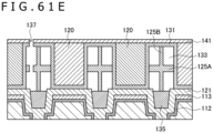
- the trench has a larger width and thus needs to be closed by a film having a larger thickness. In such a case, each distance between on-chip lenses and photoelectric conversion elements increases, and therefore a light collection property of the image sensor deteriorates.
- an internal space surrounded by the first wall portion 131 of the wall-shaped structure portion 130 constitutes the void 133 having a refractive index of approximately 1. Because the refractive index of the void 133 is thus considerably low, the wall-shaped structure portion 130 more easily satisfies conditions required for incident light to achieve total reflection on an interface between the void 133 and the first wall portion 131. Accordingly, the wall-shaped structure portion 130 is capable of more efficiently reflecting light entering the wall-shaped structure portion 130 on the interface between the void 133 and the first wall portion 131, and thus achieves more reduction of crosstalk caused by incident light coming over the wall-shaped structure portion 130 into the adjoining pixel 12.
- the openings 137 of the pixel unit 13 are formed only in a partial region of the first wall portion 131 constituting the upper surface of the wall-shaped structure portion 130. Accordingly, the closing film 140 is capable of closing the openings 137 formed in the first wall portion 131 constituting the upper surface of the wall-shaped structure portion 130 even if the closing film 140 has a smaller film thickness. According to the imaging device 1 of the present embodiment, therefore, each distance between the photoelectric conversion units 110 and the on-chip lenses 150 is allowed to further decrease. Accordingly, reduction of crosstalk between the pixels 12 is achievable without deteriorating a light collection property achieved by the on-chip lenses 150.
- each of the openings 137 closed by the closing film 140 can function as a waveguide having a waveguide effect for introducing incident light.
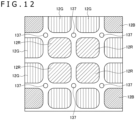
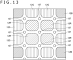
- the openings 137 may be formed between a larger number of the pixels located in diagonal directions in the pixels 12 arrayed in a matrix shape.
- the opening 137 may be formed between the pixels 12 located in diagonal directions and each adjacent to the pixel receiving light in the same color.
- the opening 137 closed by the closing film 140 is capable of more intensely introducing incident light to the respective pixels 12 provided adjacently to each other to receive light in the same color.
- FIG. 5 is a vertical cross-sectional diagram depicting the first modification of the wall-shaped structure portion 130.
- a second wall portion 132 may be further provided inside the first wall portion 131 of the wall-shaped structure portion 130.
- the second wall portion 132 includes an insulating material identical to the insulating material constituting the closing film 140 and is provided in a region located inside the wall-shaped structure portion 130 and facing the void 133.
- the light shielding portion 135 reduces crosstalk between the pixels 12 by shielding incident light passing between the pixels 12 from a lower portion of the wall-shaped structure portion 130. However, an amount of light entering each of the photoelectric conversion units 110 decreases by the shield of the incident light. Accordingly, in a case where crosstalk between the pixels 12 can be sufficiently reduced by the void 133 inside the wall-shaped structure portion 130, the light shielding portion 135 may be eliminated so as to increase the incident light entering the photoelectric conversion units 110.
- FIGS. 8 and 9 are vertical cross-sectional diagram depicting the fourth modification of the wall-shaped structure portion 130.
- the light shielding portion 135 provided in the lower part of the void 133 may have a smaller width than that of the lower part of the void 133.
- the light shielding portion 135 provided in the lower part of the void 133 may have a larger width than that of the lower part of the void 133.
- the light shielding portion 135 reduces crosstalk between the pixels 12, but decreases the amount of light entering each of the photoelectric conversion units 110. Accordingly, the size of the width of the light shielding portion 135 may be selected in consideration of a balance between reduction of crosstalk between the pixels 12, and the amount of light entering each of the photoelectric conversion units 110.
- the light shielding portion 135 may have a smaller width than that of the lower part of the void 133 so as to increase the incident light entering the photoelectric conversion units 110.
- the light shielding portion 135 may have a larger width than that of the lower part of the void 133 so as to further reduce crosstalk between the pixels 12.
- FIGS. 10 and 11 are vertical cross-sectional diagram depicting the fifth modification of the wall-shaped structure portion 130.
- the light shielding portion 135 provided in the lower part of the void 133 may be located above a lower surface of a photoelectric conversion unit 110 side of the color filter 120.
- the light shielding portion 135 provided in the lower part of the void 133 may be located below the lower surface of the photoelectric conversion unit 110 side of the color filter 120.
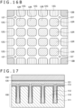
- FIG. 16B is a plan diagram depicting the second modification of the pixel unit 13.
- the pixel unit 13 according to the second modification may include sets of the red pixels 12R, the green pixels 12G, and the blue pixel 12B, each set being constituted by the adjoining 4 ⁇ 4 pixels 12.
- the pixel unit 13 may have what is called a 4 ⁇ 4 Bayer array where each set of the 4 ⁇ 4 pixels 12 contains the red pixel 12R, the green pixel 12G, or the blue pixels 12B.
- the arrangement of the openings 137 of the pixel unit 13 according to the second modification is not limited to the example depicted in FIG. 16B . Each of the arrangements depicted in FIGS. 12 to 15 may be similarly applied.
- TiN is deposited on the flattening film 121 to form the light shielding portion 135.
- AlCu aluminum containing copper
- a-Si amorphous silicon
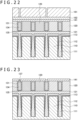
- the color filters 120 are formed in the areas corresponding to the pixels 12. Specifically, an ultraviolet curing resin containing a pigment of red, green, or blue is applied to each of areas from which the temporary wall portion 134 has been removed by photolithography or other methods. Thereafter, the ultraviolet curing resin is cured by ultraviolet light to form the color filters 120. The areas where the color filters 120 are formed are separated for each of the pixels 12 via the temporary wall portion 134. Accordingly, each of the color filters 120 can be formed in a more stable shape.
- a color arrangement of the color filters 120 provided for each of the pixels 12 may be a 2 ⁇ 2 Bayer array, a 3 ⁇ 3 Bayer array, or a 4 ⁇ 4 Bayer array as described above.
- a lower layer anti-reflection film 162 and a resist layer 161 are sequentially formed on the cap layer 141.
- the resist layer 161 includes an ordinary photoresist material and is patterned by photolithography such that areas constituting the openings 137 are opened in the following step.
- the lower layer anti-reflection film 162 is what is called a BARC film and reduces reflection on a bottom surface of the resist layer 161 during exposure of the resist layer 161 so as to prevent interference between incident light for exposure and reflection light.
- the openings 137 are formed by etching the lower layer anti-reflection film 162, the cap layer 141, and the first wall portion 131 with use of the resist layer 161 as a mask.
- the temporary wall portion 134 is exposed via the openings 137. Note that the resist layer 161 and the lower layer anti-reflection film 162 are removed after the openings 137 are formed.
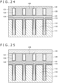
- the temporary wall portion 134 is removed by wet etching or dry etching to form the void 133.
- a tetramethylammonium hydroxide (TMAH) solution or the like is introduced into the first wall portion 131 via the openings 137 to remove the temporary wall portion 134 and form the void 133.
- TMAH tetramethylammonium hydroxide
- the temporary wall portion 134 includes AlCu
- a mixed solution of phosphoric acid, hydrogen peroxide solution, and water is introduced into the inside of the first wall portion 131 via the openings 137 to remove the temporary wall portion 134 and form the void 133.
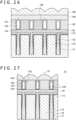
- the on-chip lens 150 is formed on the closing film 140 for each of the pixels 12.
- the temporary wall portion 134, and the first wall portion 131 covering the upper surface and the side surface of the temporary wall portion 134 are formed, and then only the temporary wall portion 134 is removed via the openings 137 formed in the first wall portion 131 to form the wall-shaped structure portion 130.
- This configuration allows the imaging device 1 to have a more reduced film thickness of the closing film 140 for closing the openings 137. Accordingly, more reduction of crosstalk between the pixels 12 is achievable by using the wall-shaped structure portion 130 without deteriorating the light collection property.
- FIG. 27 is a vertical cross-sectional diagram depicting one example of a cross-sectional configuration of the pixel unit 13 according to the present embodiment.
- each of the pixels 12 of the pixel unit 13 includes the photoelectric conversion unit 110, the flattening film 121, the color filter 120, the wall-shaped structure portion 130, and the on-chip lens 150.
- Configurations of the photoelectric conversion unit 110, the flattening film 121, the color filter 120, and the on-chip lens 150 are substantially similar to the corresponding configurations described in the first embodiment, and therefore will not be repeatedly explained herein.
- the wall-shaped structure portion 130 is a partition provided between the respective pixels 12 and has an external shape defined by a first wall portion 136 including an insulating material. Specifically, the wall-shaped structure portion 130 is defined by the first wall portion 136 which surrounds a side plane of a grid-shaped space between the pixels 12 planarly arranged in a matrix shape and an upper plane of a light receiving surface side .
- An internal space surrounded by the first wall portion 136 of the wall-shaped structure portion 130 constitutes the void 133 having a refractive index of approximately 1. Because the refractive index of the void 133 is considerably lower than the refractive index of the first wall portion 136, the wall-shaped structure portion 130 more easily satisfies conditions required for incident light to achieve total reflection on an interface between the void 133 and the first wall portion 136. Accordingly, the wall-shaped structure portion 130 is capable of more efficiently reflecting light entering the wall-shaped structure portion 130 on the interface between the void 133 and the first wall portion 136, and thus achieves more reduction of crosstalk caused by incident light coming over the wall-shaped structure portion 130 into the adjoining pixel 12.
- the foregoing structure of the wall-shaped structure portion 130 is formed by the following method, for example. Initially, a temporary wall portion is formed in a grid shape in areas between the pixels 12 by using resin decomposable in the following stage. Thereafter, the first wall portion 136 is formed on a side surface and an upper surface of the temporary wall portion to cover the temporary wall portion. According to the second embodiment, the first wall portion 136 to be provided has a porous structure. In this case, the temporary wall portion inside the first wall portion 136 is easily decomposed and removed by a chemical solution penetrating the first wall portion 136, ultraviolet light passing through the first wall portion 136, or the like. Accordingly, the void 133 can be formed inside the first wall portion 136 of the wall-shaped structure portion 130 without forming openings in the upper surface of the first wall portion 136.
- the first wall portion 136 having the porous structure can be formed by depositing a mixture of an organic material and an inorganic insulating material constituting the first wall portion 136 with use of CVD or other methods, and then selectively removing the organic material.
- the inorganic insulating material forms a firm mutual network, while the organic material is present dispersedly within the network of the inorganic insulating material.
- the first wall portion 136 thus formed has a structure containing a large number of holes corresponding to the organic material in the network of the inorganic insulating material (i.e., porous structure) after selective removal of the organic material.
- Examples of this type of organic material include ⁇ -terpinen (ATRP) which is volatilized by exposure to ultraviolet light or the like.
- Examples of the inorganic insulating material include diethoxymethylsilane (DEMS) which is a precursor of SiO x .
- DEMS diethoxymethylsilane
- a precursor of an inorganic insulating material such as Si, SiO 2 , SiN, SiC, SiCO, SiON, SiCN, SiH, SiOH, SiNH, SiCH, SiCOH, SiONH, or SiCNH may be used as the inorganic insulating material.
- first wall portion 136 may include a known porous low-k material other than the materials presented above as long as a porous structure is provided.
- the light shielding portion 135 may be provided in a lower portion of the void 133 inside the wall-shaped structure portion 130.
- the light shielding portion 135 is provided as a single-layer film including titanium (Ti), titanium nitride (TiN), tantalum (Ta), or tantalum nitride (TaN), each of which is a light shielding material, or a laminated film of these materials.
- the light shielding portion 135 can achieve further reduction of crosstalk between the pixels 12 by shielding incident light passing between the pixels 12 from a lower portion of the wall-shaped structure portion 130.
- openings are not formed in the upper surface of the first wall portion 136.
- a closing film for closing the openings is not provided on the light receiving surface side of the color filters 120. Accordingly, each height of the pixels 12 in the pixel unit 13 of the second embodiment can be further reduced.
- FIGS. 28A to 28D are vertical cross-sectional diagram explaining one step of the manufacturing method of the pixel unit 13 according to the present embodiment.
- the flattening film 121 is formed on the semiconductor layer 100 where the photoelectric conversion unit 110 is provided for each of the pixels 12 by the step depicted in FIG. 17 . Thereafter, the light shielding portion 135 and the temporary wall portion 134 are sequentially formed on the flattening film 121. Thereafter, the light shielding portion 135 and the temporary wall portion 134 in the areas corresponding to the pixels 12 are removed by the step depicted in FIG. 18 .
- the temporary wall portion 134 includes organic resin volatilized by exposure to ultraviolet light (e.g., ATRP).
- inorganic insulating material and organic material as mixed material constituting the first wall portion 136 is deposited on the flattening film 121 and the temporary wall portion 134 by CVD or other methods to form the first wall portion 136 on the upper surface and the side surface of the temporary wall portion 134.
- the organic material contained in the first wall portion 136 may be organic resin volatilized by exposure to ultraviolet light (e.g., ATRP).
- the organic material contained in the first wall portion 136 is selectively removed, and the temporary wall portion 134 is removed by exposure to ultraviolet light and heating. In this manner, the void 133 having a refractive index of approximately 1 is formed inside the first wall portion 136.
- the color filters 120 are formed in the areas corresponding to the pixels 12. Specifically, an ultraviolet curing resin containing a pigment of red, green, or blue is applied to each side area of the first wall portion 136 where the void 133 is formed inside. Then, the ultraviolet curing resin is cured by ultraviolet light to form the color filters 120. The areas where the color filters 120 are formed are separated for each of the pixels 12 via the first wall portion 136. Accordingly, each of the color filters 120 can be formed in a more stable shape.
- the color arrangement of the color filters 120 provided for each of the pixels 12 may be a 2 ⁇ 2 Bayer array, a 3 ⁇ 3 Bayer array, or a 4 ⁇ 4 Bayer array.
- the on-chip lens 150 is formed on the color filter 120 and the first wall portion 136 for each of the pixels 12. In the manner described above, the pixel unit 13 according to the second embodiment is manufactured.
- the temporary wall portion 134 in the pixel unit 13 of the second embodiment can be removed without forming openings in the first wall portion 136. Accordingly, the steps for forming the wall-shaped structure portion 130 can be simplified. Moreover, the height of the pixel unit 13 of the second embodiment is further reduced by eliminating a closing film formed on the color filters 120. Accordingly, crosstalk between the pixels 12 can be reduced by the wall-shaped structure portion 130 without deteriorating the light collection property.
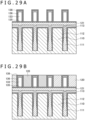
- FIGS. 29A to 30B Modifications of the pixel unit 13 according to the present embodiment will be subsequently described with reference to FIGS. 29A to 30B .
- FIGS. 29A to 29C is a vertical cross-sectional diagram explaining one step of a manufacturing method of the pixel unit 13 according to a first modification.
- FIGS. 30A to 30B is a vertical cross-sectional diagram explaining one step of a manufacturing method of the pixel unit 13 according to a second modification.
- a wall portion protection film 138 may be further provided on the first wall portion 136 and the flattening film 121 after the step depicted in FIG. 28B .
- the wall portion protection film 138 includes an inorganic insulating material such as silicon oxide (SiO x ), silicon nitride (SiN), or silicon oxynitride (SiON) and is provided along shapes of the first wall portion 136 and the flattening film 121.
- the wall portion protection film 138 can protect the first wall portion 136 which has strength lowered by the porous structure from a manufacturing process in the following stage.
- a filter protection film 151 may be further provided on the color filters 120 and the wall portion protection film 138 after the step depicted in FIG. 29B .
- the filter protection film 151 includes an inorganic insulating material such as silicon oxide (SiO x ), silicon nitride (SiN), or silicon oxynitride (SiON) and is provided on the color filters 120 and the wall portion protection film 138.
- the filter protection film 151 can protect the color filters 120 from the manufacturing process in the following stage and flatten unevenness of the color filters 120 and the wall portion protection film 138.
- the on-chip lens 150 is formed on the filter protection film 151 for each of the pixels 12.
- FIG. 31 is a vertical cross-sectional diagram depicting one example of a cross-sectional configuration of the pixel unit 13 according to the present embodiment.
- each of the pixels 12 of the pixel unit 13 includes the photoelectric conversion unit 110, the flattening film 121, the color filter 120, the wall-shaped structure portion 130, the closing film 140, and the on-chip lens 150.
- Configurations of the photoelectric conversion unit 110, the flattening film 121, the color filter 120, and the on-chip lens 150 are substantially similar to the corresponding configurations described in the first embodiment, and therefore will not be repeatedly explained herein.
- the wall-shaped structure portion 130 is a partition provided between the respective pixels 12 and has an external shape defined by the first wall portion 131 including an insulating material. Specifically, the wall-shaped structure portion 130 is defined by the first wall portion 131 which surrounds a side plane of a grid-shaped space between the pixels 12 planarly arranged in a matrix shape. Moreover, the first wall portion 131 is not provided on the upper plane of the wall-shaped structure portion 130 on the light receiving surface side. The opened upper plane of the first wall portion 131 is closed by the closing film 140 provided on the wall-shaped structure portion 130.
- the void 133 having a refractive index of approximately 1. Because the refractive index of the void 133 is considerably lower than the refractive index of the first wall portion 131, the wall-shaped structure portion 130 more easily satisfies conditions required for incident light to achieve total reflection on the interface between the void 133 and the first wall portion 131. Accordingly, the wall-shaped structure portion 130 is capable of more efficiently reflecting light entering the wall-shaped structure portion 130 on the interface between the void 133 and the first wall portion 131, and thus achieves more reduction of crosstalk caused by incident light coming over the wall-shaped structure portion 130 into the adjoining pixel 12.
- the light shielding portion 135 may be provided in a lower portion of the void 133 inside the wall-shaped structure portion 130.
- the light shielding portion 135 is provided as a single-layer film including titanium (Ti), titanium nitride (TiN), tantalum (Ta), or tantalum nitride (TaN), each of which is a light shielding material, or a laminated film of these materials.
- the light shielding portion 135 can achieve further reduction of crosstalk between the pixels 12 by shielding incident light passing between the pixels 12 from a lower portion of the wall-shaped structure portion 130.
- the closing film 140 is continuously provided on the light receiving surface side of the color filters 120 and extends through the multiple pixels 12.
- the closing film 140 includes an insulating material such as silicon oxide (SiO x ), silicon nitride (SiN), or silicon oxynitride (SiON).
- the second wall portion 132 is formed by entrance of a material constituting the closing film 140 into an inner side surface of the first wall portion 131 at the time of formation of the closing film 140 closing the upper plane of the wall-shaped structure portion 130.
- the second wall portion 132 having a uniform thickness may be formed on the inner surface of the first wall portion 131 and on the upper surface of the light shielding portion 135.
- the upper plane of the first wall portion 131 is uniformly opened, and the opened upper plane of the first wall portion 131 is closed by the closing film 140.
- the void 133 can be more reliably formed between the color filters 120 without using openings (through holes) in the pixel unit 13 of the third embodiment. Accordingly, crosstalk caused between the pixels 12 in the pixel unit 13 of the third embodiment can be more reliably reduced by the wall-shaped structure portion 130.
- the closing film 140 may have a smaller thickness than that in the case of the pixel unit 13 depicted in FIG. 31 .
- the closing film 140 has a large thickness to close the opened upper plane of the first wall portion 131.
- the height of the pixel unit 13 increases. In this case, crosstalk between the pixels 12 is difficult to reduce. Accordingly, the thickness of the closing film 140 may be reduced by CMP.
- the first wall portion 131 and the color filters 120 are simultaneously etched back when the upper surface of the first wall portion 131 is opened. Accordingly, heights of the first wall portion 131 and the color filters 120 may differ from each other depending on a difference between respective etching volumes during etching back. According to the pixel unit 13 of the present embodiment, the closing film 140 provided on the first wall portion 131 and the color filters 120 can absorb the height difference between the first wall portion 131 and the color filters 120. Accordingly, even in the foregoing case, the void 133 can be appropriately formed between the color filters 120 in the pixel unit 13 of the present embodiment.
- widths of the respective color filters 120 may differ from each other.
- Each distance between the pixels 12 is variable according to the arrangement of the pixels 12. For example, in a case where the pixels 12 are uniformly disposed in a matrix shape in an up-down direction and a left-right direction crossing each other at right angles, distances between the pixels 12 in each of the up-down direction and the left-right direction may be different from distances between the pixels in diagonal directions. Even in such a case, the void 133 can be formed between the color filters 120 in the pixel unit 13 of the present embodiment by appropriately controlling the formed film thickness of the closing film 140 provided on the first wall portion 131 and the color filters 120.
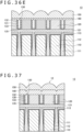
- FIGS. 36A to 36E are vertical cross-sectional diagram explaining one step of the manufacturing method of the pixel unit 13 according to the present embodiment.
- the flattening film 121, the light shielding portion 135, the temporary wall portion 134, the first wall portion 131, and the color filters 120 are sequentially formed on the semiconductor layer 100 where the photoelectric conversion unit 110 is provided for each of the pixels 12 by the steps depicted in FIGS. 17 to 20 .
- the first wall portion 131 and the color filters 120 are uniformly etched back by using dry etching, wet etching, CMP, or other methods.
- the first wall portion 131 provided on the upper surface of the temporary wall portion 134 is removed to open the upper plane of the first wall portion 131 and thus expose the temporary wall portion 134.
- the exposed temporary wall portion 134 is selectively removed.
- the temporary wall portion 134 includes AlCu
- the temporary wall portion 134 can be removed by wet etching using a mixed solution of phosphoric acid, hydrogen peroxide solution, and water.
- the temporary wall portion 134 can be removed by dry etching using SF 6 without bias.
- SiON having a large thickness is deposited on the first wall portion 131 and the color filters 120 by a low coverage film forming method, such as CVD, to form the closing film 140.
- the closing film 140 closes the opened upper plane of the first wall portion 131 to form the void 133.
- the on-chip lens 150 is formed on the closing film 140 for each of the pixels 12.
- the pixel unit 13 according to the third embodiment is manufactured.
- the forming step of the wall-shaped structure portion 130 including the void 133 in the pixel unit 13 of the third embodiment can be more simplified. Accordingly, crosstalk caused between the pixels 12 in the pixel unit 13 of the third embodiment can be reduced by the wall-shaped structure portion 130 produced at lower cost.
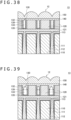
- FIG. 37 is a vertical cross-sectional diagram depicting one example of a cross-sectional configuration of the pixel unit 13 according to the present embodiment.
- each of the pixels 12 of the pixel unit 13 includes the photoelectric conversion unit 110, the flattening film 121, the color filter 120, the wall-shaped structure portion 130, the closing film 140, and the on-chip lens 150.
- Configurations of the photoelectric conversion unit 110, the flattening film 121, the color filter 120, and the on-chip lens 150 are substantially similar to the corresponding configurations described in the first embodiment, and therefore will not be repeatedly explained herein.
- the wall-shaped structure portion 130 is a partition provided between the respective pixels 12 and has an external shape defined by a first wall portion 139 including an insulating material. Specifically, the wall-shaped structure portion 130 is defined by the first wall portion 139 which surrounds a side plane of a grid-shaped space between the pixels 12 planarly arranged in a matrix shape. Moreover, the first wall portion 139 is not provided on the upper plane of the wall-shaped structure portion 130 on the light receiving surface side. The opened upper plane of the first wall portion 139 is closed by the closing film 140 provided on the wall-shaped structure portion 130.
- the void 133 having a refractive index of approximately 1. Because the refractive index of the void 133 is thus considerably lower than the refractive index of the first wall portion 139, the wall-shaped structure portion 130 more easily satisfies conditions required for incident light to achieve total reflection on an interface between the void 133 and the first wall portion 139. Accordingly, the wall-shaped structure portion 130 is capable of more efficiently reflecting light entering the wall-shaped structure portion 130 on the interface between the void 133 and the first wall portion 139, and thus achieves more reduction of crosstalk caused by incident light coming over the wall-shaped structure portion 130 into the adjoining pixel 12.
- the first wall portion 139 includes an inorganic insulating material such as silicon oxide (SiO x ), silicon nitride (SiN), or silicon oxynitride (SiON) and is provided on the side surfaces of the color filters 120.
- the first wall portion 139 may include an insulating material either identical to or different from the insulating material of the flattening film 121.
- the light shielding portion 135 may be provided in a lower portion of the void 133 inside the wall-shaped structure portion 130.
- the light shielding portion 135 is provided as a single-layer film including titanium (Ti), titanium nitride (TiN), tantalum (Ta), or tantalum nitride (TaN), each of which is a light shielding material, or a laminated film of these materials.
- the light shielding portion 135 can achieve further reduction of crosstalk between the pixels 12 by shielding incident light passing between the pixels 12 from a lower portion of the wall-shaped structure portion 130.
- the closing film 140 is continuously provided on the light receiving surface side of the color filters 120 and extends through the multiple pixels 12.
- the closing film 140 includes an insulating material such as silicon oxide (SiO x ), silicon nitride (SiN), or silicon oxynitride (SiON).
- the upper plane of the first wall portion 139 is uniformly opened, and the opened upper plane of the first wall portion 139 is closed by the closing film 140.
- the void 133 can be more reliably formed between the color filters 120 without using openings (through holes) in the pixel unit 13 of the fourth embodiment. Accordingly, crosstalk caused between the pixels 12 in the pixel unit 13 of the fourth embodiment can be more reliably reduced by the wall-shaped structure portion 130.
- FIGS. 38 to 40 are vertical cross-sectional diagram explaining a modification of the pixel unit 13 according to the present embodiment.
- the closing film 140 may have a smaller thickness than that in the case depicted in FIG. 37 .
- the closing film 140 has a large thickness to close the opened upper plane of the first wall portion 139.
- the height of the pixel unit 13 increases. In this case, crosstalk between the pixels 12 is difficult to reduce. Accordingly, the thickness of the closing film 140 may be reduced by CMP.
- widths of the respective color filters 120 may differ from each other.
- Each distance between the pixels 12 is variable according to the arrangement of the pixels 12. For example, in a case where the pixels 12 are uniformly disposed in a matrix shape in an up-down direction and a left-right direction crossing each other at right angles, distances between the pixels 12 in each of the up-down direction and the left-right direction can be mutually different from distances between the pixels in diagonal directions. Even in such a case, the void 133 can be formed between the color filters 120 in the pixel unit 13 of the present embodiment by appropriately controlling the formed film thickness of the closing film 140 provided on the first wall portion 139 and the color filters 120.
- a configuration above the flattening film 121 i.e., a light entering surface side
- a configuration below the flattening film 121 i.e., the side opposite to the light entering surface side.
- Such a shift is called pupil correction and applied to the pixels 12 provided in a region corresponding to a larger incident angle of light, such as a periphery of a pixel region.
- the centers of the on-chip lens 150, the closing film 140, the wall-shaped structure portion 130, and the color filter 120 may be shifted in the light entering direction with respect to the centers of the photoelectric conversion unit 110 and the flattening film 121.
- the pixel unit 13 according to the present embodiment is capable of more efficiently introducing light entering at a larger incident angle into the photoelectric conversion units 110. Accordingly, the pixel unit 13 according to the present embodiment is capable of more efficiently introducing light into the photoelectric conversion units 110 even with the pixels 12 provided in the periphery of the pixel region.
- the pupil correction described above can be performed not only for the pixel unit 13 of the fourth embodiment, but also for the pixel units 13 of the first to third embodiments, and the pixel unit 13 of a fifth embodiment described below in a similar manner.
- the configuration above the flattening film 121 may be similarly shifted in the light entering direction with respect to the configuration below the flattening film 121.
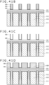
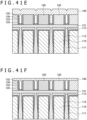
- FIGS. 41A to 41G are vertical cross-sectional diagram explaining one step of the manufacturing method of the pixel unit 13 according to the present embodiment.
- the flattening film 121, the light shielding portion 135, and the temporary wall portion 134 are sequentially formed on the semiconductor layer 100 where the photoelectric conversion unit 110 is provided for each of the pixels 12 by the steps depicted in FIGS. 17 and 18 .
- SiO x , SiN, SiON, or the like is deposited on the flattening film 121 and the temporary wall portion 134 by a high coverage film forming method to form the first wall portion 139 on the upper surface and the side surface of the temporary wall portion 134.
- the first wall portion 139 is uniformly etched back by using dry etching, wet etching, CMP, or other methods. Specifically, the first wall portion 139 provided on the flattening film 121, and the first wall portion 139 provided on the temporary wall portion 134 are removed by dry etching, wet etching, CMP, or other methods. In this manner, the first wall portion 139 provided on the upper surface of the temporary wall portion 134 is removed to open the upper surface of the first wall portion 139 and thus expose the temporary wall portion 134.
- the exposed temporary wall portion 134 is selectively removed.
- the temporary wall portion 134 can be removed by wet etching using a mixed solution of phosphoric acid, hydrogen peroxide solution, and water.
- the temporary wall portion 134 can be removed by dry etching using SF 6 without bias. In this manner, only the light shielding portion 135, and the first wall portion 139 extending in the normal direction of the surface of the flattening film 121 from both sides of the light shielding portion 135 are provided on the flattening film 121.
- the color filters 120 are formed in areas corresponding to the pixels 12. Specifically, an ultraviolet curing resin containing a pigment of red, green, or blue is applied to each of areas where the light shielding portion 135 and the first wall portion 139 are not provided. Then, the ultraviolet curing resin is cured by ultraviolet light to form the color filters 120. Each of the color filters 120 is formed in an area having a side surface defined by the temporary wall portion 134, and therefore is allowed to have a more stable shape.
- the color arrangement of the color filters 120 provided for each of the pixels 12 may be a 2 ⁇ 2 Bayer array, a 3 ⁇ 3 Bayer array, or a 4 ⁇ 4 Bayer array.
- SiON having a large thickness is deposited on the first wall portion 139 and the color filters 120 by a low coverage film forming method, such as CVD, to form the closing film 140.
- the closing film 140 thus formed closes the opened upper plane of the first wall portion 139 to form the void 133.
- the thickness of the closing film 140 is reduced by CMP to such an extent that closure of the void 133 by the closing film 140 is not destroyed. Note that the thickness of the closing film 140 is not required to be reduced.
- the on-chip lens 150 is formed on the closing film 140 for each of the pixels 12.
- the pixel unit 13 according to the fourth embodiment is manufactured.
- the forming step of the wall-shaped structure portion 130 including the void 133 in the pixel unit 13 of the fourth embodiment can be more simplified. Accordingly, crosstalk caused between the pixels 12 in the pixel unit 13 of the fourth embodiment can be reduced by the wall-shaped structure portion 130 produced at lower cost.
- FIG. 42 is a vertical cross-sectional diagram depicting one example of a cross-sectional configuration of the pixel unit 13 according to the present embodiment.
- the stopper layer 122 includes an insulating material having an etching rate different from that of the color filters 120 and is provided on the flattening film 121.
- the stopper layer 122 reduces progress of etching up to a lower layer of the stopper layer 122 at the time of etching for separating the color filters 120 for each of the pixels 12.
- the wall-shaped structure portion 130 includes a first wall portion 1312 and the void 133 and is provided in a space between the color filters 120 separated by etching.
- the first wall portion 1312 is formed by entrance of a material constituting the closing film 140 into the space between the color filters 120 at the time of formation of the closing film 140 for closing an upper plane of the space between the color filters 120.
- the first wall portion 1312 can be provided on the side surfaces of the color filters 120 and on an upper surface of the stopper layer 122.
- the void 133 is formed by closure of the upper plane of the space between the color filters 120 with use of the closing film 140.
- the filter protection film 151 includes an inorganic insulating material such as silicon oxide (SiO x ), silicon nitride (SiN), or silicon oxynitride (SiON) and is provided on the color filters 120.
- the filter protection film 151 is provided to protect the color filters 120 from a manufacturing process performed in the following stage.
- the filter protection film 151 can protect the color filters 120 from a process for separating resist used in an etching step for the color filters 120.
- the closing film 140 is continuously provided on the light receiving surface side of the filter protection film 151 and extends through the multiple pixels 12.
- the closing film 140 includes an insulating material such as silicon oxide (SiO x ), silicon nitride (SiN), or silicon oxynitride (SiON).
- the closing film 140 having a large thickness is formed on the filter protection film 151 by a low coverage film forming method, such as CVD, and therefore can close the upper plane of the space between the respective color filters 120.
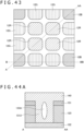
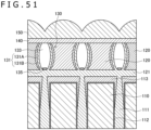
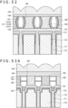
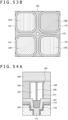
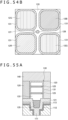
- FIG. 43 is a plan diagram depicting a planar configuration of the pixel unit 13 according to the fifth embodiment.
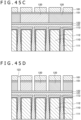
- FIG. 44A is a vertical cross-sectional diagram depicting a cross-sectional configuration taken along a cutting plane A-AA in FIG. 43
- FIG. 44B is a vertical cross-sectional diagram depicting a cross-sectional configuration taken along a cutting plane B-BB in FIG. 43 .
- the pixel unit 13 may have the pixels 12 including red pixels 12R, green pixels 12G, and blue pixels 12B and planarly arranged in a matrix shape.
- spaces between the color filters 120 included in the pixels 12 arrayed in a matrix shape and located in diagonal directions are relatively wide.
- the closing film 140 is easily embedded in these spaces, and the first wall portion 1312 to be formed easily has a large thickness.
- spaces between the color filters 120 included in the pixels 12 arrayed in a matrix shape and located in row directions or column directions are relatively narrow. In this case, these spaces are easily closed by the closing film 140, and the first wall portion 1312 to be formed easily has a smaller thickness.
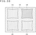
- a void 133A included in the pixels 12 and formed in a space between the color filters 120 located in a diagonal direction can be made smaller than a void 133B included in the pixels 12 and formed in a space between the color filters 120 located in a row direction or a column direction.
- the closing film 140 closes the upper plane of the space between the color filters 120 separated from each other for each of the pixels 12 by etching. Accordingly, the pixel unit 13 of the fifth embodiment is capable of stabilizing the shape of the color filters 120 by a more simplified method. Moreover, crosstalk caused between the pixels 12 in the pixel unit 13 of the fifth embodiment can be reduced by the void 133 formed between the color filters 120.
- FIGS. 45A to 45F are vertical cross-sectional diagram explaining one step of the manufacturing method of the pixel unit 13 according to the present embodiment.
- the flattening film 121 is formed on the semiconductor layer 100 where the photoelectric conversion unit 110 is provided for each of the pixels 12. Thereafter, the stopper layer 122 is sequentially formed on the flattening film 121.
- the stopper layer 122 may include SiN or SiON having an etching rate different from that of the color filters 120 and is provided on the flattening film 121 with a film thickness in a range of 10 to 15 nm.
- the color filters 120 are formed in areas corresponding to the pixels 12. Specifically, an ultraviolet curing resin containing a pigment of red, green, or blue is applied to each of the areas corresponding to the pixels 12. Then, the ultraviolet curing resin is cured by ultraviolet light to form the color filters 120.
- the color filters 120 are patterned for each of the pixels 12 by an etching process in the following stage. Accordingly, the areas where the color filters 120 are provided are only required to roughly coincide with the areas corresponding to the pixels 12.
- the filter protection film 151 and the resist layer 161 are formed on the color filters 120.
- SiON is initially deposited on the color filters 120 to form the filter protection film 151.
- the resist layer 161 is formed on the filter protection film 151.
- the resist layer 161 includes an ordinary photoresist material and is patterned by photolithography such that areas forming openings 123 are opened in the following step.
- the openings 123 are formed in areas corresponding to the areas between the pixels 12 by etching the filter protection film 151 and the color filters 120 with use of the resist layer 161 as a mask.
- the stopper layer 122 having an etching rate different from that of the color filters 120 is provided below the color filters 120. Accordingly, etching of the color filters 120 is stopped at the surface of the stopper layer 122.
- the respective color filters 120 of the pixel unit 13 according to the fifth embodiment can be separated for each of the pixels 12 by etching. Accordingly, the shape of the color filters 120 can be more easily stabilized. Moreover, crosstalk caused between the pixels 12 in the pixel unit 13 of the fifth embodiment can be reduced by the void 133 formed between the respective color filters 120.
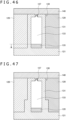
- the light shielding portion 135 is provided in the inner space surrounded by the first wall portion 131.
- the light shielding portion 135 is provided as a single-layer film including titanium (Ti), titanium nitride (TiN), tantalum (Ta), or tantalum nitride (TaN), each of which is a light shielding material, or a laminated film of these materials.
- the light shielding portion 135 can achieve reduction of crosstalk between the pixels 12 by shielding incident light passing between the pixels 12 from a lower portion of the wall-shaped structure portion 130.
- FIG. 48 is a vertical cross-sectional diagram explaining one step of the manufacturing method of the pixel unit 13 according to the present embodiment.
- the pixel unit 13 of the sixth embodiment can lower the magnitude of the tensile stress acting on the first wall portion 131 on the side surface side by controlling the respective positions of the lower ends of the color filters 120 and the void 133. Accordingly, the pixel unit 13 of the sixth embodiment can further lower the possibility of crack generation in the first wall portion 131 on the side surface side.
- each of the pixels 12 of the pixel unit 13 includes the photoelectric conversion unit 110, the flattening film 121, the color filter 120, the wall-shaped structure portion 130, the closing film 140, and the on-chip lens 150.
- Configurations of the photoelectric conversion unit 110, the flattening film 121, the color filter 120, the closing film 140, and the on-chip lens 150 are substantially similar to the configurations described in the first embodiment, and therefore will not be repeated herein.
- the wall-shaped structure portion 130 is a partition provided between the respective pixels 12 and has an external shape defined by a first wall portion 131 including an insulating material.
- the light shielding portion 135 having a light shielding property is provided in a lower part of the void 133 inside the wall-shaped structure portion 130, while the upper plane of the wall-shaped structure portion 130 (i.e., the opened upper plane of the first wall portion 131) is closed by the closing film 140.
- An internal space whose side plane is surrounded by the first wall portion 131 of the wall-shaped structure portion 130 constitutes the void 133 having a refractive index of approximately 1.
- the partition 125 is provided so as to extend in the horizontal direction and divide the void 133 into two upper and lower spaces.
- the partition 125 may include an insulating material such as silicon oxide (SiO x ), silicon nitride (SiN), or silicon oxynitride (SiON).
- the closing film 140 and the on-chip lenses 150 are formed by the steps depicted in FIGS. 25 and 26 to manufacture the second configuration example of the pixel unit 13 according to the eighth embodiment.
- the closing film 140 and the on-chip lenses 150 are formed by the steps depicted in FIGS. 25 and 26 to manufacture the third configuration example of the pixel unit 13 according to the eighth embodiment.
- the optical lens 1001 forms an image of incident light coming from a subject on an imaging surface of the imaging device 1.
- the shutter device 1002 controls irradiation or shielding of the incident light to and from the imaging device 1.
- the microcomputer 12051 can perform cooperative control intended for automated driving, which makes the vehicle to travel automatedly without depending on the operation of the driver, or the like, by controlling the driving force generating device, the steering mechanism, the braking device, or the like on the basis of the information about the outside or inside of the vehicle which information is obtained by the outside-vehicle information detecting unit 12030 or the in-vehicle information detecting unit 12040.
- the imaging sections 12101, 12102, 12103, 12104, and 12105 are, for example, disposed at positions on a front nose, sideview mirrors, a rear bumper, and a back door of the vehicle 12100 as well as a position on an upper portion of a windshield within the interior of the vehicle.
- the imaging section 12101 provided to the front nose and the imaging section 12105 provided to the upper portion of the windshield within the interior of the vehicle obtain mainly an image of the front of the vehicle 12100.
- the imaging sections 12102 and 12103 provided to the sideview mirrors obtain mainly an image of the sides of the vehicle 12100.
- the imaging section 12104 provided to the rear bumper or the back door obtains mainly an image of the rear of the vehicle 12100.
- the imaging section 12105 provided to the upper portion of the windshield within the interior of the vehicle is used mainly to detect a preceding vehicle, a pedestrian, an obstacle, a signal, a traffic sign, a lane, or the like.
- FIG. 64 depicts an example of photographing ranges of the imaging sections 12101 to 12104.
- An imaging range 12111 represents the imaging range of the imaging section 12101 provided to the front nose.
- Imaging ranges 12112 and 12113 respectively represent the imaging ranges of the imaging sections 12102 and 12103 provided to the sideview mirrors.
- An imaging range 12114 represents the imaging range of the imaging section 12104 provided to the rear bumper or the back door.
- a bird's-eye image of the vehicle 12100 as viewed from above is obtained by superimposing image data imaged by the imaging sections 12101 to 12104, for example.
- At least one of the imaging sections 12101 to 12104 may have a function of obtaining distance information.
- at least one of the imaging sections 12101 to 12104 may be a stereo camera constituted of a plurality of imaging elements, or may be an imaging element having pixels for phase difference detection.
- the microcomputer 12051 can classify three-dimensional object data on three-dimensional objects into three-dimensional object data of a two-wheeled vehicle, a standard-sized vehicle, a large-sized vehicle, a pedestrian, a utility pole, and other three-dimensional objects on the basis of the distance information obtained from the imaging sections 12101 to 12104, extract the classified three-dimensional object data, and use the extracted three-dimensional object data for automatic avoidance of an obstacle.
- the microcomputer 12051 identifies obstacles around the vehicle 12100 as obstacles that the driver of the vehicle 12100 can recognize visually and obstacles that are difficult for the driver of the vehicle 12100 to recognize visually. Then, the microcomputer 12051 determines a collision risk indicating a risk of collision with each obstacle.
- the microcomputer 12051 In a situation in which the collision risk is equal to or higher than a set value and there is thus a possibility of collision, the microcomputer 12051 outputs a warning to the driver via the audio speaker 12061 or the display section 12062, and performs forced deceleration or avoidance steering via the driving system control unit 12010. The microcomputer 12051 can thereby assist in driving to avoid collision.
- At least one of the imaging sections 12101 to 12104 may be an infrared camera that detects infrared rays.
- the microcomputer 12051 can, for example, recognize a pedestrian by determining whether or not there is a pedestrian in imaged images of the imaging sections 12101 to 12104. Such recognition of a pedestrian is, for example, performed by a procedure of extracting characteristic points in the imaged images of the imaging sections 12101 to 12104 as infrared cameras and a procedure of determining whether or not it is the pedestrian by performing pattern matching processing on a series of characteristic points representing the contour of the object.
- the sound/image output section 12052 controls the display section 12062 so that a square contour line for emphasis is displayed so as to be superimposed on the recognized pedestrian.
- the sound/image output section 12052 may also control the display section 12062 so that an icon or the like representing the pedestrian is displayed at a desired position.
- the technology according to the present disclosure is applicable to the imaging section 12031 in the configuration described above.
- a higher-sensitivity captured image is acquirable by applying the technology of the present disclosure to the imaging section 12031. Accordingly, recognition of an obstacle or a pedestrian on the basis of a captured image is achievable with higher sensitivity, for example.
- a higher-sensitivity captured image is presentable by applying the technology of the present disclosure to the imaging section 12031, for example. Accordingly, a driver is allowed to achieve observation around the driver with higher sensitivity.
Landscapes
- Engineering & Computer Science (AREA)
- Multimedia (AREA)
- Signal Processing (AREA)
- Physics & Mathematics (AREA)
- Spectroscopy & Molecular Physics (AREA)
- Solid State Image Pick-Up Elements (AREA)
- Color Television Image Signal Generators (AREA)
Abstract
Description
- The present disclosure relates to an imaging device and an electronic apparatus.
- A CCD (Charge Coupled Device) image sensor or a CMOS (Complementary Metal Oxide Semiconductor) image sensor is known as an imaging device included in a digital camera or a video camera.
- For these types of image sensors, it has been studied to form a void between respective color filters provided for pixels with one-to-one correspondence so as to reduce crosstalk between the pixels. For example,
PTL 1 identified below discloses an image sensor which has a void formed by closing, with a low coverage film, openings above a trench provided between respective color filters. -
- However, in a case where the void has a larger width to achieve more reduction of crosstalk between pixels in the image sensor disclosed in
PTL 1 disclosed above, the trench has a larger width and thus needs to be closed by a film having a larger thickness. In such a case, each distance between on-chip lenses and photoelectric conversion elements increases, and therefore a light collection property of the image sensor deteriorates. - Accordingly, the present disclosure proposes an imaging device and an electronic apparatus each of which is novel and improved, and capable of achieving more improvement of sensitivity by reducing crosstalk between pixels without deteriorating a light collection property.
- Provided according to the present disclosure is an imaging device including multiple pixels each including a photoelectric conversion unit, and planarly arranged in a matrix shape, a color filter provided on the photoelectric conversion unit for each of the pixels, and a wall-shaped structure portion that is formed between the adjoining color filters with an external shape of the wall-shaped structure portion defined by a first wall portion, and is configured to separate the color filters from each other.
- In addition, provided according to the present disclosure is an electronic apparatus including an imaging device. The imaging device includes multiple pixels each including a photoelectric conversion unit, and planarly arranged in a matrix shape, a color filter provided on the photoelectric conversion unit for each of the pixels, and a wall-shaped structure portion that is formed between the adjoining color filters with an external shape of the wall-shaped structure portion defined by a first wall portion, and is configured to separate the color filters from each other.
-
- [
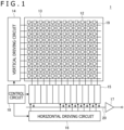
FIG. 1 ]
FIG. 1 is a schematic diagram depicting a general configuration of an imaging device according to a first embodiment of the present disclosure. - [
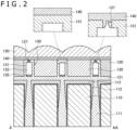
FIG. 2 ]
FIG. 2 is a vertical cross-sectional diagram depicting one example of a cross-sectional configuration of a pixel unit. - [
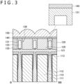
FIG. 3 ]
FIG. 3 is a vertical cross-sectional diagram depicting one example of the cross-sectional configuration of the pixel unit. - [
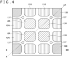
FIG. 4 ]
FIG. 4 is a plan diagram depicting a planar configuration of the pixel unit. - [
FIG. 5 ]
FIG. 5 is a vertical cross-sectional diagram depicting a first modification of a wall-shaped structure portion. - [
FIG. 6A ]
FIG. 6A is a vertical cross-sectional diagram depicting a second modification of the wall-shaped structure portion. - [
FIG. 6B ]
FIG. 6B is a vertical cross-sectional diagram depicting the second modification of the wall-shaped structure portion. - [
FIG. 7 ]
FIG. 7 is a vertical cross-sectional diagram depicting a third modification of the wall-shaped structure portion. - [
FIG. 8 ]
FIG. 8 is a vertical cross-sectional diagram depicting a fourth modification of the wall-shaped structure portion. - [
FIG. 9 ]
FIG. 9 is a vertical cross-sectional diagram depicting the fourth modification of the wall-shaped structure portion. - [
FIG. 10 ]
FIG. 10 is a vertical cross-sectional diagram depicting a fifth modification of the wall-shaped structure portion. - [
FIG. 11 ]
FIG. 11 is a vertical cross-sectional diagram depicting the fifth modification of the wall-shaped structure portion. - [
FIG. 12 ]
FIG. 12 is a plan diagram depicting a first modification of arrangement of openings. - [
FIG. 13 ]
FIG. 13 is a plan diagram depicting a second modification of the arrangement of the openings. - [
FIG. 14 ]
FIG. 14 is a plan diagram depicting a third modification of the arrangement of the openings. - [
FIG. 15 ]
FIG. 15 is a plan diagram depicting a fourth modification of the arrangement of the openings. - [
FIG. 16A ]
FIG. 16A is a plan diagram depicting a first modification of the pixel unit. - [
FIG. 16B ]
FIG. 16B is a plan diagram depicting a second modification of the pixel unit. - [
FIG. 17 ]
FIG. 17 is a vertical cross-sectional diagram explaining one step of a manufacturing method of the pixel unit. - [
FIG. 18 ]
FIG. 18 is a vertical cross-sectional diagram explaining one step of the manufacturing method of the pixel unit. - [
FIG. 19 ]
FIG. 19 is a vertical cross-sectional diagram explaining one step of the manufacturing method of the pixel unit. - [
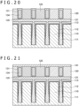
FIG. 20 ]
FIG. 20 is a vertical cross-sectional diagram explaining one step of the manufacturing method of the pixel unit. - [
FIG. 21 ]
FIG. 21 is a vertical cross-sectional diagram explaining one step of the manufacturing method of the pixel unit. - [
FIG. 22 ]
FIG. 22 is a vertical cross-sectional diagram explaining one step of the manufacturing method of the pixel unit. - [
FIG. 23 ]
FIG. 23 is a vertical cross-sectional diagram explaining one step of the manufacturing method of the pixel unit. - [
FIG. 24 ]
FIG. 24 is a vertical cross-sectional diagram explaining one step of the manufacturing method of the pixel unit. - [
FIG. 25 ]
FIG. 25 is a vertical cross-sectional diagram explaining one step of the manufacturing method of the pixel unit. - [
FIG. 26 ]
FIG. 26 is a vertical cross-sectional diagram explaining one step of the manufacturing method of the pixel unit. - [
FIG. 27 ]
FIG. 27 is a vertical cross-sectional diagram depicting one example of a cross-sectional configuration of the pixel unit according to a second embodiment. - [
FIG. 28A ]
FIG. 28A is a vertical cross-sectional diagram explaining one step of a manufacturing method of a pixel unit according to the second embodiment. - [
FIG. 28B ]
FIG. 28B is a vertical cross-sectional diagram explaining one step of the manufacturing method of the pixel unit according to the second embodiment. - [
FIG. 28C ]
FIG. 28C is a vertical cross-sectional diagram explaining one step of the manufacturing method of the pixel unit according to the second embodiment of the present disclosure. - [
FIG. 28D ]
FIG. 28D is a vertical cross-sectional diagram explaining one step of the manufacturing method of the pixel unit according to the second embodiment. - [
FIG. 29A ]
FIG. 29A is a vertical cross-sectional diagram explaining one step of a manufacturing method of a pixel unit according to a first modification of the second embodiment. - [
FIG. 29B ]
FIG. 29B is a vertical cross-sectional diagram explaining one step of the manufacturing method of the pixel unit according to the first modification of the second embodiment. - [
FIG. 29C ]
FIG. 29C is a vertical cross-sectional diagram explaining one step of the manufacturing method of the pixel unit according to the first modification of the second embodiment. - [
FIG. 30A ]
FIG. 30A is a vertical cross-sectional diagram explaining one step of a manufacturing method of a pixel unit according to a second modification of the second embodiment. - [
FIG. 30B ]
FIG. 30B is a vertical cross-sectional diagram explaining one step of the manufacturing method of the pixel unit according to the second modification of the second embodiment. - [
FIG. 31 ]
FIG. 31 is a vertical cross-sectional diagram depicting one example of a cross-sectional configuration of a pixel unit according to a third embodiment. - [
FIG. 32 ]
FIG. 32 is a vertical cross-sectional diagram explaining a modification of the pixel unit according to the third embodiment. - [
FIG. 33 ]
FIG. 33 is a vertical cross-sectional diagram explaining a modification of the pixel unit according to the third embodiment. - [
FIG. 34 ]
FIG. 34 is a vertical cross-sectional diagram explaining a modification of the pixel unit according to the third embodiment. - [
FIG. 35 ]
FIG. 35 is a vertical cross-sectional diagram explaining a modification of the pixel unit according to the third embodiment. - [
FIG. 36A ]
FIG. 36A is a vertical cross-sectional diagram explaining one step of a manufacturing method of the pixel unit according to the third embodiment. - [
FIG. 36B ]
FIG. 36B is a vertical cross-sectional diagram explaining one step of the manufacturing method of the pixel unit according to the third embodiment. - [
FIG. 36C ]
FIG. 36C is a vertical cross-sectional diagram explaining one step of the manufacturing method of the pixel unit according to the third embodiment. - [
FIG. 36D ]
FIG. 36D is a vertical cross-sectional diagram explaining one step of the manufacturing method of the pixel unit according to the third embodiment. - [
FIG. 36E ]
FIG. 36E is a vertical cross-sectional diagram explaining one step of the manufacturing method of the pixel unit according to the third embodiment. - [
FIG. 37 ]
FIG. 37 is a vertical cross-sectional diagram depicting one example of a cross-sectional configuration of a pixel unit according to a fourth embodiment. - [
FIG. 38 ]
FIG. 38 is a vertical cross-sectional diagram explaining a modification of the pixel unit according to the fourth embodiment. - [
FIG. 39 ]
FIG. 39 is a vertical cross-sectional diagram explaining a modification of the pixel unit according to the fourth embodiment. - [
FIG. 40 ]
FIG. 40 is a vertical cross-sectional diagram explaining a modification of the pixel unit according to the fourth embodiment. - [
FIG. 41A ]
FIG. 41A is a vertical cross-sectional diagram explaining one step of a manufacturing method of the pixel unit according to the fourth embodiment. - [
FIG. 41B ]
FIG. 41B is a vertical cross-sectional diagram explaining one step of the manufacturing method of the pixel unit according to the fourth embodiment. - [
FIG. 41C ]
FIG. 41C is a vertical cross-sectional diagram explaining one step of the manufacturing method of the pixel unit according to the fourth embodiment. - [
FIG. 41D ]
FIG. 41D is a vertical cross-sectional diagram explaining one step of the manufacturing method of the pixel unit according to the fourth embodiment. - [
FIG. 41E ]
FIG. 41E is a vertical cross-sectional diagram explaining one step of the manufacturing method of the pixel unit according to the fourth embodiment. - [
FIG. 41F ]
FIG. 41F is a vertical cross-sectional diagram explaining one step of the manufacturing method of the pixel unit according to the fourth embodiment. - [
FIG. 41G ]
FIG. 41G is a vertical cross-sectional diagram explaining one step of the manufacturing method of the pixel unit according to the fourth embodiment. - [
FIG. 42 ]
FIG. 42 is a vertical cross-sectional diagram depicting one example of a cross-sectional configuration of a pixel unit according to a fifth embodiment. - [
FIG. 43 ]
FIG. 43 is a plan diagram depicting a planar configuration of the pixel unit according to the fifth embodiment. - [
FIG. 44A ]
FIG. 44A is a vertical cross-sectional diagram depicting a cross-sectional configuration taken along a cutting plane A-AA inFIG. 43 . - [
FIG. 44B ]
FIG. 44B is a vertical cross-sectional diagram depicting a cross-sectional configuration taken along a cutting plane B-BB inFIG. 43 . - [
FIG. 45A ]
FIG. 45A is a vertical cross-sectional diagram explaining one step of a manufacturing method of the pixel unit according to the fifth embodiment. - [
FIG. 45B ]
FIG. 45B is a vertical cross-sectional diagram explaining one step of the manufacturing method of the pixel unit according to the fifth embodiment. - [
FIG. 45C ]
FIG. 45C is a vertical cross-sectional diagram explaining one step of the manufacturing method of the pixel unit according to the fifth embodiment. - [
FIG. 45D ]
FIG. 45D is a vertical cross-sectional diagram explaining one step of the manufacturing method of the pixel unit according to the fifth embodiment. - [
FIG. 45E ]
FIG. 45E is a vertical cross-sectional diagram explaining one step of the manufacturing method of the pixel unit according to the fifth embodiment. - [
FIG. 45F ]
FIG. 45F is a vertical cross-sectional diagram explaining one step of the manufacturing method of the pixel unit according to the fifth embodiment. - [
FIG. 46 ]
FIG. 46 is a vertical cross-sectional diagram depicting a cross-sectional configuration of the wall-shaped structure portion included in a pixel unit according to a sixth embodiment. - [
FIG. 47 ]
FIG. 47 is a vertical cross-sectional diagram depicting a first modification of the wall-shaped structure portion. - [
FIG. 48 ]
FIG. 48 is a vertical cross-sectional diagram explaining one step of a manufacturing method of the pixel unit according to the sixth embodiment. - [
FIG. 49 ]
FIG. 49 is a vertical cross-sectional diagram depicting one example of a cross-sectional configuration of the pixel unit according to the sixth embodiment. - [
FIG. 50 ]
FIG. 50 is a plan diagram depicting a planar configuration of the pixel unit according to the sixth embodiment. - [
FIG. 51 ]
FIG. 51 is a vertical cross-sectional diagram explaining a first modification of the pixel unit according to the sixth embodiment. - [
FIG. 52 ]
FIG. 52 is a vertical cross-sectional diagram explaining a second modification of the pixel unit according to the sixth embodiment. - [
FIG. 53A ]
FIG. 53A is a vertical cross-sectional diagram depicting a cross section of a first configuration example of a pixel unit according to a seventh embodiment. - [
FIG. 53B ]
FIG. 53B is a plan diagram depicting a plane of the first configuration example of the pixel unit according to the seventh embodiment. - [
FIG. 54A ]
FIG. 54A is a vertical cross-sectional diagram depicting a cross section of a second configuration example of the pixel unit according to the seventh embodiment. - [
FIG. 54B ]
FIG. 54B is a plan diagram depicting a plane of the second configuration example of the pixel unit according to the seventh embodiment. - [
FIG. 55A ]
FIG. 55A is a vertical cross-sectional diagram depicting a cross section of a third configuration example of the pixel unit according to the seventh embodiment. - [
FIG. 55B ]
FIG. 55B is a plan diagram depicting a plane of the third configuration example of the pixel unit according to the seventh embodiment. - [
FIG. 56A ]
FIG. 56A is a vertical cross-sectional diagram depicting a cross section of a fourth configuration example of the pixel unit according to the seventh embodiment. - [
FIG. 56B ]
FIG. 56B is a plan diagram depicting a plane of the fourth configuration example of the pixel unit according to the seventh embodiment. - [
FIG. 57A ]
FIG. 57A is a vertical cross-sectional diagram depicting a cross section of a fifth configuration example of the pixel unit according to the seventh embodiment. - [
FIG. 57B ]
FIG. 57B is a plan diagram depicting a plane of the fifth configuration example of the pixel unit according to the seventh embodiment. - [
FIG. 58A ]
FIG. 58A is a vertical cross-sectional diagram depicting a cross section of a sixth configuration example of the pixel unit according to the seventh embodiment. - [
FIG. 58B ]
FIG. 58B is a plan diagram depicting a plane of the sixth configuration example of the pixel unit according to the seventh embodiment. - [
FIG. 59A ]
FIG. 59A is a vertical cross-sectional diagram explaining a manufacturing method of the first configuration example of the pixel unit according to the seventh embodiment. - [
FIG. 59B ]
FIG. 59B is a vertical cross-sectional diagram explaining the manufacturing method of the first configuration example of the pixel unit according to the seventh embodiment. - [
FIG. 59C ]
FIG. 59C is a vertical cross-sectional diagram explaining the manufacturing method of the first configuration example of the pixel unit according to the seventh embodiment. - [
FIG. 59D ]
FIG. 59D is a vertical cross-sectional diagram explaining the manufacturing method of the first configuration example of the pixel unit according to the seventh embodiment. - [
FIG. 59E ]
FIG. 59E is a vertical cross-sectional diagram explaining the manufacturing method of the first configuration example of the pixel unit according to the seventh embodiment. - [
FIG. 59F ]
FIG. 59F is a vertical cross-sectional diagram explaining the manufacturing method of the first configuration example of the pixel unit according to the seventh embodiment. - [
FIG. 60A ]
FIG. 60A is a vertical cross-sectional diagram explaining a manufacturing method of the fourth configuration example of the pixel unit according to the seventh embodiment. - [
FIG. 60B ]
FIG. 60B is a vertical cross-sectional diagram explaining the manufacturing method of the fourth configuration example of the pixel unit according to the seventh embodiment. - [
FIG. 60C ]
FIG. 60C is a vertical cross-sectional diagram explaining the manufacturing method of the fourth configuration example of the pixel unit according to the seventh embodiment. - [
FIG. 60D ]
FIG. 60D is a vertical cross-sectional diagram explaining the manufacturing method of the fourth configuration example of the pixel unit according to the seventh embodiment. - [
FIG. 61A ]
FIG. 61A is a vertical cross-sectional diagram explaining a manufacturing method of the fifth configuration example of the pixel unit according to the seventh embodiment. - [
FIG. 61B ]
FIG. 61B is a vertical cross-sectional diagram explaining the manufacturing method of the fifth configuration example of the pixel unit according to the seventh embodiment. - [
FIG. 61C ]
FIG. 61C is a vertical cross-sectional diagram explaining the manufacturing method of the fifth configuration example of the pixel unit according to the seventh embodiment. - [
FIG. 61D ]
FIG. 61D is a vertical cross-sectional diagram explaining the manufacturing method of the fifth configuration example of the pixel unit according to the seventh embodiment. - [
FIG. 61E ]
FIG. 61E is a vertical cross-sectional diagram explaining the manufacturing method of the fifth configuration example of the pixel unit according to the seventh embodiment. - [
FIG. 62 ]
FIG. 62 is a block diagram depicting a configuration example of an electronic apparatus including an imaging device according to one embodiment of the present disclosure. - [
FIG. 63 ]
FIG. 63 is a block diagram depicting an example of schematic configuration of a vehicle control system. - [
FIG. 64 ]
FIG. 64 is a diagram of assistance in explaining an example of installation positions of an outside-vehicle information detecting section and an imaging section. - Preferred embodiments of the present disclosure will be hereinafter explained in detail with reference to the accompanying drawings. Note that constituent elements having substantially identical functional configurations in the present description and the drawings will be given identical reference signs to omit repetitive explanation.
- Note that the explanation will be presented in the following order.
- 1. First embodiment
- 1.1. General configuration of imaging device
- 1.2. Configuration of pixel unit
- 1.3. Manufacturing method
- 2. Second embodiment
- 2.1. Configuration of pixel unit
- 2.2. Manufacturing method
- 2.3. Modifications
- 3. Third embodiment
- 3.1. Configuration of pixel unit
- 3.2. Modifications
- 3.3. Manufacturing method
- 4. Fourth embodiment
- 4.1. Configuration of pixel unit
- 4.2. Modifications
- 4.3. Manufacturing method
- 5. Fifth embodiment
- 5.1. Configuration of pixel unit
- 5.2. Manufacturing method
- 6. Sixth embodiment
- 6.1. Configuration of pixel unit
- 6.2. Modifications
- 6.3. Manufacturing method
- 7. Seventh embodiment
- 7.1. Configuration of pixel unit
- 7.2. Modifications
- 8. Eighth embodiment
- 8.1. Configuration of pixel unit
- 8.2. Manufacturing method
- 9. Electronic apparatus
- 10. Application example
- A general configuration of an imaging device according to a first embodiment of the present disclosure will be initially described with reference to
FIG. 1. FIG. 1 is a schematic diagram depicting a general configuration of animaging device 1 according to the present embodiment. - As depicted in
FIG. 1 , theimaging device 1 includes apixel unit 13 includingmultiple pixels 12 provided on a semiconductor substrate, avertical driving circuit 14, columnsignal processing circuits 15, ahorizontal driving circuit 16, anoutput circuit 17, and acontrol circuit 18. - The
pixel unit 13 includes themultiple pixels 12 planarly arranged on a semiconductor substrate in a matrix shape. For example, each of thepixels 12 includes a photoelectric conversion unit containing a photodiode, and a pixel circuit containing a transfer transistor, an amplification transistor, a selection transistor, and a reset transistor. Note that the pixel circuit is not required to contain the selection transistor. Signal charge output from the photodiode is amplified by the pixel circuit to be converted into a pixel signal. - Moreover, the
pixels 12 to be provided may have a shared pixel structure. According to the shared pixel structure, a part or the whole of the pixel circuit is shared by the multiple adjoiningpixels 12. For example, each of the multiple adjoiningpixels 12 may share a pixel circuit containing an amplification transistor, a selection transistor, and a reset transistor provided in a stage subsequent to a transfer transistor. Specifically, each pixel circuit of the multiple adjoiningpixels 12 may include an own photodiode, an own transfer transistor, one shared floating diffusion (floating diffusion region: FD), one shared amplification transistor, one shared selection transistor, and one shared reset transistor. - The
control circuit 18 controls operations of the respective units of theimaging device 1. Specifically, thecontrol circuit 18 generates clock signals and control signals as operation references of thevertical driving circuit 14, the columnsignal processing circuits 15, and thehorizontal driving circuit 16 on the basis of vertical synchronized signals, horizontal synchronized signals, and master clocks. Thecontrol circuit 18 is capable of controlling the operations of thevertical driving circuit 14, the columnsignal processing circuits 15, and thehorizontal driving circuit 16 on the basis of the generated clock signals and control signals. - For example, the
vertical driving circuit 14 includes a shift register. Thevertical driving circuit 14 selectively scans thepixels 12 sequentially in the vertical direction for each row to drive thepixels 12 for each row. In this manner, thevertical driving circuit 14 is capable of reading a pixel signal generated according to a received light amount from each of thepixels 12 and supplying the read pixel signal to the corresponding columnsignal processing circuit 15 via a vertical signal line 19. - The column
signal processing circuit 15 is provided for each column of thepixels 12 to perform signal processing such as noise removal for pixel signals output from thepixels 12. For example, each of the columnsignal processing circuits 15 may perform correlative double sampling (CDS) processing for removing pattern noise unique to each of thepixels 12, AD (Analog-Digital) conversion processing, and the like for pixel signals output from thepixels 12. - For example, the
horizontal driving circuit 16 includes a shift register. Thehorizontal driving circuit 16 sequentially outputs a horizontal scanning pulse and sequentially selects the respective columnsignal processing circuits 15 to cause the respective columnsignal processing circuits 15 to output pixel signals to ahorizontal signal line 20. - The
output circuit 17 outputs, to the outside of theimaging device 1, pixel signals sequentially supplied from the respective columnsignal processing circuits 15 via thehorizontal signal line 20. For example, theoutput circuit 17 may perform buffering, black level adjustment, various types of digital signal processing such as column variation correction, or the like for pixel signals supplied from the respective columnsignal processing circuits 15, and then output the signal-processed pixel signals to the outside of theimaging device 1. - The
imaging device 1 having the foregoing configuration is what is called a column AD type CMOS (Complementary MOS) image sensor which includes the columnsignal processing circuit 15 performing CDS processing and AD conversion processing for each column of thepixels 12. - A configuration of the
pixel unit 13 of theimaging device 1 according to the present embodiment will be subsequently described with reference toFIGS. 2 to 4 . Each ofFIGS. 2 and3 is a vertical cross-sectional diagram depicting one example of a cross-sectional configuration of thepixel unit 13, whileFIG. 4 is a plan diagram depicting a planar configuration of thepixel unit 13. The cross-sectional configuration depicted inFIG. 2 corresponds to a cross-sectional configuration taken along a cutting plane A-AA inFIG. 4 , while the cross-sectional configuration depicted inFIG. 3 corresponds to a cross-sectional configuration taken along a cutting plane B-BB inFIG. 4 . - As depicted in
FIGS. 2 and3 , each of thepixels 12 of thepixel unit 13 includes aphotoelectric conversion unit 110, a flatteningfilm 121, acolor filter 120, a wall-shapedstructure portion 130, aclosing film 140, and an on-chip lens 150. - The
photoelectric conversion unit 110 is provided for each of thepixels 12. The respectivephotoelectric conversion units 110 are separated from each other by apixel separation layer 111. Each of thephotoelectric conversion units 110 is a photodiode and is produced by joining a first conductivity-type (e.g., p-type) semiconductor region and a second conductivity-type (e.g., n-type) semiconductor region by PN junction. For example, thephotoelectric conversion units 110 may be produced by forming a p-type well region in a semiconductor layer including silicon (Si) or the like and providing an n-type region for each of thepixels 12 inside the p-type well region. - Note that a circuit layer which includes a pixel circuit for converting signal charge photoelectrically converted by the
photoelectric conversion unit 110 into a pixel signal is provided on a surface of each of thephotoelectric conversion units 110 on the side opposite to a light receiving surface (i.e., a surface where the on-chip lens 150 is provided). Accordingly, theimaging device 1 of the present embodiment is what is called a back-illuminated imaging device. - The
pixel separation layer 111 includes an insulating material and is provided so as to extend in a normal direction of a plane where thepixels 12 are arrayed to separate thephotoelectric conversion units 110 for each of thepixels 12. In other words, thepixel separation layer 111 is provided so as to extend in a thickness direction of a semiconductor layer where thephotoelectric conversion units 110 are provided to separate thephotoelectric conversion units 110 for each of thepixels 12. Thepixel separation layer 111 may include an insulating material such as silicon oxide (SiOx), silicon nitride (SiN), or silicon oxynitride (SiON). - A pinning
layer 112 is provided on each surface of thephotoelectric conversion units 110 and on each interface between thephotoelectric conversion units 110 and thepixel separation layer 111. The pinninglayer 112 includes a high dielectric material having negative fixed charge, such as hafnium oxide (HfO2), zirconium oxide (ZrO2), aluminum oxide (Al2O3), tantalum oxide (Ta2O5), titanium oxide (TiO2), magnesium oxide (MgO), yttrium oxide (Y2O3), or an oxide of lanthanoid. The pinninglayer 112 forms a region where holes are accumulated on the surfaces of thephotoelectric conversion units 110 and the interfaces between thephotoelectric conversion units 110 and thepixel separation layer 111 to reduce generation of dark current in thephotoelectric conversion units 110. - Moreover, an
anti-reflection layer 113 is provided on each of thephotoelectric conversion units 110 on the light receiving surface side of the pinninglayer 112 in such a manner as to cover thephotoelectric conversion units 110. Theanti-reflection layer 113 thus provided includes an insulating material having a refractive index lower than a refractive index of the high dielectric material constituting the pinninglayer 112. Theanti-reflection layer 113 thus configured can further reduce reflection of light entering theanti-reflection layer 113 and the pinninglayer 112 from the on-chip lens 150 side corresponding to the light receiving surface side. For example, theanti-reflection layer 113 may include tantalum oxide (Ta2O5). - The flattening
film 121 is uniformly provided on the light receiving surface side of theanti-reflection layer 113 continuously through themultiple pixels 12. For example, the flatteningfilm 121 may include an insulating material having high light transparency (e.g., light transmittance of approximately 70% or higher in a visible light band), such as silicon oxide (SiOx), silicon nitride (SiN), or silicon oxynitride (SiON). - The flattening
film 121 may be provided continuously with thepixel separation layer 111. Specifically, the flatteningfilm 121 and thepixel separation layer 111 each including an insulating material such as SiOx may be continuously formed. In such a case, the flatteningfilm 121 and thepixel separation layer 111 are allowed to be formed by the same step. Accordingly, manufacturing steps of theimaging device 1 can be more simplified. - Provided on the light receiving surface side of the flattening
film 121 are thecolor filters 120 separated from each other by the wall-shapedstructure portion 130 for each of thepixels 12. For example, each of thecolor filters 120 may be formed by applying organic resin containing a pigment presenting red, green, or blue to an area of the correspondingpixel 12. - For example, as depicted in
FIG. 4 , thepixel unit 13 may have thepixels 12 includingred pixels 12R,green pixels 12G, andblue pixels 12B and planarly arranged in a matrix shape. Each of thered pixels 12R is a pixel containing a red color filter and receiving red light. Each of thegreen pixels 12G is a pixel containing a green color filter and receiving green light. Each of theblue pixels 12B is a pixel containing a blue color filter and receiving blue light. Thepixel unit 13 may include sets of thered pixels 12R, thegreen pixels 12G, and theblue pixel 12B, each set being constituted by the adjoining 2 × 2pixels 12. Specifically, for example, thepixel unit 13 may have what is called a 2 × 2 Bayer array where each set of the 2 × 2pixels 12 contains thered pixel 12R, thegreen pixel 12G, or theblue pixels 12B. - The wall-shaped
structure portion 130 is a partition provided between therespective pixels 12 and has an external shape defined by afirst wall portion 131 including an insulating material. Specifically, the wall-shapedstructure portion 130 is defined by thefirst wall portion 131 which surrounds a side plane of a grid-shaped space between thepixels 12 planarly arranged in a matrix shape and an upper plane of a light receiving surface side. - In this case, an internal space surrounded by the
first wall portion 131 of the wall-shapedstructure portion 130 constitutes the void 133 having a refractive index of approximately 1. Because the refractive index of the void 133 is thus considerably low, the wall-shapedstructure portion 130 more easily satisfies conditions required for incident light to achieve total reflection on an interface between the void 133 and thefirst wall portion 131. Accordingly, the wall-shapedstructure portion 130 is capable of more efficiently reflecting light entering the wall-shapedstructure portion 130 on the interface between the void 133 and thefirst wall portion 131, and thus achieves more reduction of crosstalk caused by incident light coming over the wall-shapedstructure portion 130 into the adjoiningpixel 12. - The foregoing structure of the wall-shaped
structure portion 130, which will be described in detail below, is formed by the following method, for example. Specifically, a temporary wall portion is initially formed in a grid shape in areas between thepixels 12. Thefirst wall portion 131 is subsequently formed on a side surface and an upper surface of the temporary wall portion to cover the temporary wall portion. Thereafter, thecolor filter 120 is formed in each area of thepixels 12, and thenopenings 137 are formed in the upper surface of thefirst wall portion 131. Subsequently, the temporary wall portion inside thefirst wall portion 131 is removed by wet etching or dry etching via theopenings 137 of thefirst wall portion 131 to form thevoid 133 inside thefirst wall portion 131. In addition, after thevoid 133 is formed, theopenings 137 of thefirst wall portion 131 are closed by theclosing film 140 described below. In this manner, thevoid 133 inside the wall-shapedstructure portion 130 is sealed. - The
first wall portion 131 may be formed such that a film thickness of the upper surface of the wall-shapedstructure portion 130 becomes larger than a film thickness of the side surface of the wall-shapedstructure portion 130. The upper surface of the wall-shapedstructure portion 130 is subjected to processing such as etching, CVD (Chemical Vapor Deposition), or CMP (Chemical Mechanical Polishing) in a later stage of the manufacturing steps. Accordingly, thefirst wall portion 131 constituting the upper surface of the wall-shapedstructure portion 130 and having a larger film thickness can further raise processing resistance during the manufacturing steps. For example, thefirst wall portion 131 constituting the upper surface of the wall-shapedstructure portion 130 can prevent collapsing of thefirst wall portion 131 of the upper surface during a step of flattening upper surfaces of thecolor filters 120 and the wall-shapedstructure portion 130 by CMP after thecolor filters 120 are formed. - A
light shielding portion 135 may be provided in a lower portion of the void 133 inside the wall-shapedstructure portion 130. For example, thelight shielding portion 135 is provided as a single-layer film including titanium (Ti), titanium nitride (TiN), tantalum (Ta), or tantalum nitride (TaN), each of which is a light shielding material, or a laminated film of these materials. Thelight shielding portion 135 can achieve further reduction of crosstalk between thepixels 12 by shielding incident light passing between thepixels 12 from a lower portion of the wall-shapedstructure portion 130. - The
closing film 140 is continuously provided on the light receiving surface side of thecolor filters 120 and extend through themultiple pixels 12. For example, theclosing film 140 includes an insulating material such as silicon oxide (SiOx), silicon nitride (SiN), or silicon oxynitride (SiON). Theclosing film 140 is a film including the insulating material described above and formed on the wall-shapedstructure portion 130 and thecolor filters 120 by using a low coverage film forming method, such as CVD, to close theopenings 137 formed in thefirst wall portion 131 constituting the upper surface of the wall-shapedstructure portion 130. - The
openings 137 of thepixel unit 13 are formed only in a partial region of thefirst wall portion 131 constituting the upper surface of the wall-shapedstructure portion 130. Accordingly, theclosing film 140 is capable of closing theopenings 137 formed in thefirst wall portion 131 constituting the upper surface of the wall-shapedstructure portion 130 even if theclosing film 140 has a smaller film thickness. According to theimaging device 1 of the present embodiment, therefore, each distance between thephotoelectric conversion units 110 and the on-chip lenses 150 is allowed to further decrease. Accordingly, reduction of crosstalk between thepixels 12 is achievable without deteriorating a light collection property achieved by the on-chip lenses 150. - However, the
closing film 140 may include an insulating material having a refractive index substantially equal to a refractive index of the on-chip lenses 150 described below or smaller than the refractive index of the on-chip lenses 150. Note that the "substantially equal" refractive index mentioned above may refer to a different refractive index of theclosing film 140 from the refractive index of the on-chip lenses 150 by 0.1 or smaller. This configuration can reduce a possibility that light entering theclosing film 140 via the on-chip lenses 150 reflects on interfaces between the on-chip lenses 150 and theclosing film 140, and therefore can further increase amounts of light entering thephotoelectric conversion units 110. - For example, in a case where the on-
chip lenses 150 include ordinary organic resin for optical use (refractive index: approximately 1.5 to 1.6), theclosing film 140 may include silicon oxynitride (SiON) having a refractive index of 1.58. - For example, as depicted in
FIG. 4 , each of theopenings 137 may be provided between thepixels 12 arrayed in a matrix shape and located in diagonal directions. Each of theopenings 137 is provided in the wall-shapedstructure portion 130 between thepixels 12. Accordingly, each of theopenings 137 formed between thepixels 12 in the diagonal directions is allowed to have a larger radius in comparison with a case where each of theopenings 137 is formed between thepixels 12 in row directions or column directions. - Each of the
openings 137 is an inlet port through which a chemical solution for wet etching or an etching gas for dry etching is introduced into the inside of thefirst wall portion 131. Accordingly, the number of theopenings 137 may be reduced to such an extent that etching is allowed to progress. For example, as depicted inFIG. 4 , theopenings 137 may be provided not between all thepixels 12 located in diagonal directions, but only between the pixels located in diagonal directions and adjacent to the three types of thepixels 12 each receiving different color light (red pixel 12R,green pixel 12G, andblue pixel 12B inFIG. 4 ). - Alternatively, the
openings 137 may be formed between a larger number of the pixels located in diagonal directions. In such a case, the chemical solution or the etching gas for etching can be more efficiently introduced into the inside of thefirst wall portion 131. Accordingly, a processing time required for etching can be more shortened. - Moreover, each of the
openings 137 closed by theclosing film 140 can function as a waveguide having a waveguide effect for introducing incident light. Accordingly, theopenings 137 may be formed between a larger number of the pixels located in diagonal directions in thepixels 12 arrayed in a matrix shape. For example, theopening 137 may be formed between thepixels 12 located in diagonal directions and each adjacent to the pixel receiving light in the same color. In such a case, theopening 137 closed by theclosing film 140 is capable of more intensely introducing incident light to therespective pixels 12 provided adjacently to each other to receive light in the same color. - The on-
chip lens 150 is provided on the light receiving surface side of theclosing film 140 for each of thepixels 12. Specifically, the on-chip lens 150 is provided as a convex lens which collects incident light for each of thepixels 12. In this case, the on-chip lens 150 allows thephotoelectric conversion unit 110 provided for each of thepixels 12 to efficiently receive light. For example, the on-chip lens 150 may include transparent organic resin, such as styrene-based resin, acryl-based resin, styrene-acryl copolymerization-based resin, or siloxane-based resin, such that light transparency becomes 70% or higher in a visible light band. - According to the
imaging device 1 which includes thepixel unit 13 having the above configuration, each radius of theopenings 137 used at the time of formation of the void 133 in the wall-shapedstructure portion 130 between thepixels 12 is allowed to become smaller. In this case, theopenings 137 can be closed by theclosing film 140 having a smaller film thickness. Accordingly, theimaging device 1 can reduce crosstalk caused between thepixels 12 by using the wall-shapedstructure portion 130 containing the void 133 without deteriorating the light collection property of the on-chip lenses 150 according to a height increase. As a result, sensitivity of theimaging device 1 is allowed to improve. - Moreover, according to the
imaging device 1, the external shape of the wall-shapedstructure portion 130 is defined by thefirst wall portion 131. In this case, the shape of the void 133 formed inside the wall-shapedstructure portion 130 can be further stabilized. Accordingly, theimaging device 1 can reduce variations in crosstalk between thepixels 12. - First to fifth modifications of the wall-shaped
structure portion 130 will be subsequently described with reference toFIGS. 5 to 11 . -
FIG. 5 is a vertical cross-sectional diagram depicting the first modification of the wall-shapedstructure portion 130. As depicted inFIG. 5 , asecond wall portion 132 may be further provided inside thefirst wall portion 131 of the wall-shapedstructure portion 130. Specifically, thesecond wall portion 132 includes an insulating material identical to the insulating material constituting theclosing film 140 and is provided in a region located inside the wall-shapedstructure portion 130 and facing thevoid 133. - For example, the
second wall portion 132 is formed by entrance of a material constituting theclosing film 140 into thevoid 133 inside the wall-shapedstructure portion 130 via theopenings 137 at the time of formation of theclosing film 140 for closing theopenings 137. Accordingly, for example, thesecond wall portion 132 may be provided in thevoid 133 inside the wall-shapedstructure portion 130 located near theopenings 137, while thesecond wall portion 132 may be eliminated from thevoid 133 inside the wall-shapedstructure portion 130 located away from theopenings 137. - Each of
FIGS. 6A and6B is a vertical cross-sectional diagram depicting the second modification of the wall-shapedstructure portion 130. As depicted inFIG. 6A , the wall-shapedstructure portion 130 may have a reverse tapered shape which has a width decreasing toward thephotoelectric conversion units 110 on the side opposite to the light receiving surface. Moreover, as depicted inFIG. 6B , the wall-shapedstructure portion 130 may have a forward tapered shape which has a width increasing toward thephotoelectric conversion units 110 on the side opposite to the light receiving surface. - The external shape of the wall-shaped
structure portion 130 is defined by thefirst wall portion 131 formed on the side surface and the upper surface of the temporary wall portion (which will be removed in the following process and thus is not depicted in the figure) in a manner to cover the temporary wall portion after the temporary wall portion is formed in the region where the wall-shapedstructure portion 130 is provided. Accordingly, the wall-shapedstructure portion 130 is allowed to have any cross section having a forward tapered shape, a reverse tapered shape, or a non-tapered shape by controlling a cross-sectional shape of the temporary wall. In this case, the wall-shapedstructure portion 130 to be provided has a more stabilized cross-sectional shape. Accordingly, variations in crosstalk between thepixels 12 produced by the wall-shapedstructure portion 130 can be reduced by theentire pixel unit 13. -
FIG. 7 is a vertical cross-sectional diagram depicting the third modification of the wall-shapedstructure portion 130. As depicted inFIG. 7 , thelight shielding portion 135 may be eliminated from thevoid 133 inside the wall-shapedstructure portion 130. - The
light shielding portion 135 reduces crosstalk between thepixels 12 by shielding incident light passing between thepixels 12 from a lower portion of the wall-shapedstructure portion 130. However, an amount of light entering each of thephotoelectric conversion units 110 decreases by the shield of the incident light. Accordingly, in a case where crosstalk between thepixels 12 can be sufficiently reduced by thevoid 133 inside the wall-shapedstructure portion 130, thelight shielding portion 135 may be eliminated so as to increase the incident light entering thephotoelectric conversion units 110. - Each of
FIGS. 8 and9 is a vertical cross-sectional diagram depicting the fourth modification of the wall-shapedstructure portion 130. As depicted inFIG. 8 , thelight shielding portion 135 provided in the lower part of the void 133 may have a smaller width than that of the lower part of thevoid 133. Alternatively, as depicted inFIG. 9 , thelight shielding portion 135 provided in the lower part of the void 133 may have a larger width than that of the lower part of thevoid 133. - As described in the third modification, the
light shielding portion 135 reduces crosstalk between thepixels 12, but decreases the amount of light entering each of thephotoelectric conversion units 110. Accordingly, the size of the width of thelight shielding portion 135 may be selected in consideration of a balance between reduction of crosstalk between thepixels 12, and the amount of light entering each of thephotoelectric conversion units 110. - For example, in a case where crosstalk between the
pixels 12 can be sufficiently reduced by thevoid 133 inside the wall-shapedstructure portion 130, thelight shielding portion 135 may have a smaller width than that of the lower part of the void 133 so as to increase the incident light entering thephotoelectric conversion units 110. On the other hand, in a case where crosstalk between thepixels 12 is difficult to reduce by thevoid 133 inside the wall-shapedstructure portion 130, thelight shielding portion 135 may have a larger width than that of the lower part of the void 133 so as to further reduce crosstalk between thepixels 12. - Each of
FIGS. 10 and11 is a vertical cross-sectional diagram depicting the fifth modification of the wall-shapedstructure portion 130. As depicted inFIG. 10 , thelight shielding portion 135 provided in the lower part of the void 133 may be located above a lower surface of aphotoelectric conversion unit 110 side of thecolor filter 120. Moreover, as depicted inFIG. 11 , thelight shielding portion 135 provided in the lower part of the void 133 may be located below the lower surface of thephotoelectric conversion unit 110 side of thecolor filter 120. - A shielding ability exerted by the
light shielding portion 135 to shield incident light coming from the lower part of the wall-shapedstructure portion 130 and passing between thepixels 12 is influenced by an incident angle and an incident position of the incident light and the position of thelight shielding portion 135. Accordingly, thelight shielding portion 135 can more efficiently reduce crosstalk between thepixels 12 by adjustment of the positions of thecolor filters 120 in a film thickness direction. - First to fourth modifications of arrangement of the
openings 137 will be subsequently described with reference toFIGS. 12 to 15 . -
FIG. 12 is a plan diagram depicting the first modification of the arrangement of theopenings 137. As depicted inFIG. 12 , theopenings 137 may be provided between the pixels included in thepixels 12 arrayed in a matrix shape and located in diagonal directions, and adjacent to the three types of thepixels 12 each receiving different color light (red pixel 12R,green pixel 12G, andblue pixel 12B inFIG. 12 ), and also between the pixels arranged in the row directions or the column directions including the pixels adjacent to the three types of thepixels 12. -
FIG. 13 is a plan diagram depicting the second modification of the arrangement of theopenings 137. As depicted inFIG. 13 , theopenings 137 may be provided between all thepixels 12 arrayed in a matrix shape and located in diagonal directions. Each of theopenings 137 closed by theclosing film 140 can function as a waveguide having a waveguide effect for introducing incident light. Accordingly, the arrangement of theopenings 137 between all thepixels 12 arrayed in a matrix shape and located diagonal directions can introduce a larger amount of incident light into each of thephotoelectric conversion units 110. Moreover, in a case where a larger number of theopenings 137 are provided, thevoid 133 inside the wall-shapedstructure portion 130 is further enlarged and made uniform within thepixel unit 13. In this manner, theimaging device 1 can further reduce variations in crosstalk between thepixels 12. -
FIG. 14 is a plan diagram depicting the third modification of the arrangement of theopenings 137. As depicted inFIG. 14 , theopenings 137 may be provided between the pixels each adjacent to the pixel receiving light in the same color (red pixel 12R inFIG. 14 ) in thepixels 12 arrayed in a matrix shape and located in diagonal directions. Each of theopenings 137 closed by theclosing film 140 can function as a waveguide having a waveguide effect for introducing incident light. Accordingly, the arrangement of theopenings 137 between thepixels 12 located in diagonal directions and each adjacent to the pixel receiving light in the same color can introduce a larger amount of incident light into each of thephotoelectric conversion units 110 of thepixels 12 receiving light in the same color. -
FIG. 15 is a plan diagram depicting the fourth modification of the arrangement of theopenings 137. As depicted inFIG. 15 , theopenings 137 may be provided between the pixels included in thepixels 12 arrayed in a matrix shape and located in diagonal directions and each adjacent to thepixel 12 receiving light in the same color (red pixel 12R inFIG. 15 ), and also between the pixels arranged in the row directions or the column directions including the pixels each adjacent to thepixel 12 receiving light in the same color. Each of theopenings 137 closed by theclosing film 140 can function as a waveguide having a waveguide effect for introducing incident light. Accordingly, the arrangement of theopenings 137 between thepixels 12 including the pixels located in diagonal directions and each adjacent to the pixel receiving light in the same color can introduce a larger amount of incident light into each of thephotoelectric conversion units 110 of thepixels 12 receiving light in the same color. - First and second modifications of the
pixel unit 13 will be further described with reference toFIGS. 16A and16B . -
FIG. 16A is a plan diagram depicting the first modification of thepixel unit 13. Thepixel unit 13 according to the first modification may include sets of thered pixels 12R, thegreen pixels 12G, and theblue pixel 12B, each set being constituted by the adjoining 3 × 3pixels 12. Specifically, for example, thepixel unit 13 may have what is called a 3 × 3 Bayer array where each set of the 3 × 3pixels 12 contains thered pixel 12R, thegreen pixel 12G, or theblue pixels 12B. The arrangement of theopenings 137 of thepixel unit 13 according to the first modification is not limited to the example depicted inFIG. 16A . Each of the arrangements depicted inFIGS. 12 to 15 may be similarly applied. -
FIG. 16B is a plan diagram depicting the second modification of thepixel unit 13. Thepixel unit 13 according to the second modification may include sets of thered pixels 12R, thegreen pixels 12G, and theblue pixel 12B, each set being constituted by the adjoining 4 × 4pixels 12. Specifically, for example, thepixel unit 13 may have what is called a 4 × 4 Bayer array where each set of the 4 × 4pixels 12 contains thered pixel 12R, thegreen pixel 12G, or theblue pixels 12B. The arrangement of theopenings 137 of thepixel unit 13 according to the second modification is not limited to the example depicted inFIG. 16B . Each of the arrangements depicted inFIGS. 12 to 15 may be similarly applied. - A manufacturing method of the
pixel unit 13 according to the present embodiment will be subsequently described with reference toFIGS. 17 to 26 . Each ofFIGS. 17 to 26 is a vertical cross-sectional diagram explaining one step of the manufacturing method of thepixel unit 13. - Initially, as depicted in
FIG. 17 , the flatteningfilm 121 is formed on asemiconductor layer 100 where thephotoelectric conversion unit 110 is provided for each of thepixels 12. Thereafter, thelight shielding portion 135 and atemporary wall portion 134 are sequentially formed on theflattening film 121. - Specifically, conductivity-type impurities are initially introduced into the
semiconductor layer 100 including silicon (Si) or the like to form thephotoelectric conversion units 110. Next, thesemiconductor layer 100 in a region other than regions corresponding to thepixels 12 is removed by etching, and then the pinninglayer 112 and theanti-reflection layer 113 are formed along external shapes of thephotoelectric conversion units 110. Subsequently, spaces produced between thephotoelectric conversion units 110 after the removal by etching is filled with SiOx to form thepixel separation layer 111. Moreover, SiOx constituting thepixel separation layer 111 is further deposited up to an area above theanti-reflection layer 113 to form theflattening film 121. For example, the flatteningfilm 121 may be flattened using CMP or other methods. - Thereafter, TiN is deposited on the
flattening film 121 to form thelight shielding portion 135. Moreover, aluminum containing copper (AlCu) or amorphous silicon (a-Si) is deposited on thelight shielding portion 135 to form thetemporary wall portion 134. Thetemporary wall portion 134 will be removed by wet etching or dry etching in the following step to produce thevoid 133. - Next, as depicted in
FIG. 18 , thelight shielding portion 135 and thetemporary wall portion 134 in the areas corresponding to thepixels 12 are removed by photolithography or other methods. As a result, areas where thecolor filters 120 will be formed in the following step are opened, and thelight shielding portion 135 and thetemporary wall portion 134 in a region other than a grid-shaped region between thepixels 12 are removed from the upper part of the flatteningfilm 121. - Subsequently, as depicted in
FIG. 19 , SiOx is deposited on theflattening film 121 and thetemporary wall portion 134 by a high coverage film forming method to form thefirst wall portion 131 on an upper surface and a side surface of thetemporary wall portion 134. - Next, as depicted in
FIG. 20 , thecolor filters 120 are formed in the areas corresponding to thepixels 12. Specifically, an ultraviolet curing resin containing a pigment of red, green, or blue is applied to each of areas from which thetemporary wall portion 134 has been removed by photolithography or other methods. Thereafter, the ultraviolet curing resin is cured by ultraviolet light to form the color filters 120. The areas where thecolor filters 120 are formed are separated for each of thepixels 12 via thetemporary wall portion 134. Accordingly, each of thecolor filters 120 can be formed in a more stable shape. - Note that a color arrangement of the
color filters 120 provided for each of thepixels 12 may be a 2 × 2 Bayer array, a 3 × 3 Bayer array, or a 4 × 4 Bayer array as described above. - Subsequently, as depicted in
FIG. 21 , SiON is deposited on thecolor filters 120 and thefirst wall portion 131 to form acap layer 141. Specifically, upper surfaces of thefirst wall portion 131 and thecolor filters 120 are flattened by etching back, CMP, or other methods, and then thecap layer 141 is formed on thecolor filters 120 and thefirst wall portion 131. - Next, as depicted in
FIG. 22 , a lowerlayer anti-reflection film 162 and a resistlayer 161 are sequentially formed on thecap layer 141. The resistlayer 161 includes an ordinary photoresist material and is patterned by photolithography such that areas constituting theopenings 137 are opened in the following step. The lowerlayer anti-reflection film 162 is what is called a BARC film and reduces reflection on a bottom surface of the resistlayer 161 during exposure of the resistlayer 161 so as to prevent interference between incident light for exposure and reflection light. - Subsequently, as depicted in
FIG. 23 , theopenings 137 are formed by etching the lowerlayer anti-reflection film 162, thecap layer 141, and thefirst wall portion 131 with use of the resistlayer 161 as a mask. Thetemporary wall portion 134 is exposed via theopenings 137. Note that the resistlayer 161 and the lowerlayer anti-reflection film 162 are removed after theopenings 137 are formed. - Thereafter, as depicted in
FIG. 24 , thetemporary wall portion 134 is removed by wet etching or dry etching to form thevoid 133. Specifically, in a case where thetemporary wall portion 134 includes a-Si, a tetramethylammonium hydroxide (TMAH) solution or the like is introduced into thefirst wall portion 131 via theopenings 137 to remove thetemporary wall portion 134 and form thevoid 133. Alternatively, in a case where thetemporary wall portion 134 includes AlCu, a mixed solution of phosphoric acid, hydrogen peroxide solution, and water is introduced into the inside of thefirst wall portion 131 via theopenings 137 to remove thetemporary wall portion 134 and form thevoid 133. - Subsequently, as depicted in
FIG. 25 , SiON is deposited on thecap layer 141 by a low coverage film forming method, such as CVD, to form theclosing film 140. Thevoid 133 is shielded by closing theopenings 137 with theclosing film 140. According to the present embodiment, theopenings 137 are formed between the pixels included in the array of thepixels 12 in a matrix shape and located in diagonal directions and each have a smaller radius than a width between the pixels. Accordingly, theopenings 137 can be easily closed by theclosing film 140 even with a small thickness. - Further, as depicted in
FIG. 26 , the on-chip lens 150 is formed on theclosing film 140 for each of thepixels 12. - According to the steps described above, the
temporary wall portion 134, and thefirst wall portion 131 covering the upper surface and the side surface of thetemporary wall portion 134 are formed, and then only thetemporary wall portion 134 is removed via theopenings 137 formed in thefirst wall portion 131 to form the wall-shapedstructure portion 130. This configuration allows theimaging device 1 to have a more reduced film thickness of theclosing film 140 for closing theopenings 137. Accordingly, more reduction of crosstalk between thepixels 12 is achievable by using the wall-shapedstructure portion 130 without deteriorating the light collection property. - A configuration of the
pixel unit 13 according to a second embodiment of the present disclosure will be subsequently described with reference toFIG. 27. FIG. 27 is a vertical cross-sectional diagram depicting one example of a cross-sectional configuration of thepixel unit 13 according to the present embodiment. - As depicted in
FIG. 27 , each of thepixels 12 of thepixel unit 13 includes thephotoelectric conversion unit 110, the flatteningfilm 121, thecolor filter 120, the wall-shapedstructure portion 130, and the on-chip lens 150. Configurations of thephotoelectric conversion unit 110, the flatteningfilm 121, thecolor filter 120, and the on-chip lens 150 are substantially similar to the corresponding configurations described in the first embodiment, and therefore will not be repeatedly explained herein. - The wall-shaped
structure portion 130 is a partition provided between therespective pixels 12 and has an external shape defined by afirst wall portion 136 including an insulating material. Specifically, the wall-shapedstructure portion 130 is defined by thefirst wall portion 136 which surrounds a side plane of a grid-shaped space between thepixels 12 planarly arranged in a matrix shape and an upper plane of a light receiving surface side . - An internal space surrounded by the
first wall portion 136 of the wall-shapedstructure portion 130 constitutes the void 133 having a refractive index of approximately 1. Because the refractive index of the void 133 is considerably lower than the refractive index of thefirst wall portion 136, the wall-shapedstructure portion 130 more easily satisfies conditions required for incident light to achieve total reflection on an interface between the void 133 and thefirst wall portion 136. Accordingly, the wall-shapedstructure portion 130 is capable of more efficiently reflecting light entering the wall-shapedstructure portion 130 on the interface between the void 133 and thefirst wall portion 136, and thus achieves more reduction of crosstalk caused by incident light coming over the wall-shapedstructure portion 130 into the adjoiningpixel 12. - The foregoing structure of the wall-shaped
structure portion 130, which will be described in detail below, is formed by the following method, for example. Initially, a temporary wall portion is formed in a grid shape in areas between thepixels 12 by using resin decomposable in the following stage. Thereafter, thefirst wall portion 136 is formed on a side surface and an upper surface of the temporary wall portion to cover the temporary wall portion. According to the second embodiment, thefirst wall portion 136 to be provided has a porous structure. In this case, the temporary wall portion inside thefirst wall portion 136 is easily decomposed and removed by a chemical solution penetrating thefirst wall portion 136, ultraviolet light passing through thefirst wall portion 136, or the like. Accordingly, the void 133 can be formed inside thefirst wall portion 136 of the wall-shapedstructure portion 130 without forming openings in the upper surface of thefirst wall portion 136. - For example, the
first wall portion 136 having the porous structure can be formed by depositing a mixture of an organic material and an inorganic insulating material constituting thefirst wall portion 136 with use of CVD or other methods, and then selectively removing the organic material. In thefirst wall portion 136 after the deposition, the inorganic insulating material forms a firm mutual network, while the organic material is present dispersedly within the network of the inorganic insulating material. Accordingly, thefirst wall portion 136 thus formed has a structure containing a large number of holes corresponding to the organic material in the network of the inorganic insulating material (i.e., porous structure) after selective removal of the organic material. - Examples of this type of organic material include α-terpinen (ATRP) which is volatilized by exposure to ultraviolet light or the like. Examples of the inorganic insulating material include diethoxymethylsilane (DEMS) which is a precursor of SiOx. In addition, a precursor of an inorganic insulating material such as Si, SiO2, SiN, SiC, SiCO, SiON, SiCN, SiH, SiOH, SiNH, SiCH, SiCOH, SiONH, or SiCNH may be used as the inorganic insulating material.
- Note that the
first wall portion 136 may include a known porous low-k material other than the materials presented above as long as a porous structure is provided. - The
light shielding portion 135 may be provided in a lower portion of the void 133 inside the wall-shapedstructure portion 130. For example, thelight shielding portion 135 is provided as a single-layer film including titanium (Ti), titanium nitride (TiN), tantalum (Ta), or tantalum nitride (TaN), each of which is a light shielding material, or a laminated film of these materials. Thelight shielding portion 135 can achieve further reduction of crosstalk between thepixels 12 by shielding incident light passing between thepixels 12 from a lower portion of the wall-shapedstructure portion 130. - According to the second embodiment, openings are not formed in the upper surface of the
first wall portion 136. In this case, a closing film for closing the openings is not provided on the light receiving surface side of the color filters 120. Accordingly, each height of thepixels 12 in thepixel unit 13 of the second embodiment can be further reduced. - A manufacturing method of the
pixel unit 13 according to the present embodiment will be subsequently described with reference toFIGS. 28A to 28D . Each ofFIGS. 28A to 28D is a vertical cross-sectional diagram explaining one step of the manufacturing method of thepixel unit 13 according to the present embodiment. - Initially, similarly to the first embodiment, the flattening
film 121 is formed on thesemiconductor layer 100 where thephotoelectric conversion unit 110 is provided for each of thepixels 12 by the step depicted inFIG. 17 . Thereafter, thelight shielding portion 135 and thetemporary wall portion 134 are sequentially formed on theflattening film 121. Thereafter, thelight shielding portion 135 and thetemporary wall portion 134 in the areas corresponding to thepixels 12 are removed by the step depicted inFIG. 18 . Note that thetemporary wall portion 134 includes organic resin volatilized by exposure to ultraviolet light (e.g., ATRP). - Subsequently, as depicted in
FIG. 28A , inorganic insulating material and organic material as mixed material constituting thefirst wall portion 136 is deposited on theflattening film 121 and thetemporary wall portion 134 by CVD or other methods to form thefirst wall portion 136 on the upper surface and the side surface of thetemporary wall portion 134. The organic material contained in thefirst wall portion 136 may be organic resin volatilized by exposure to ultraviolet light (e.g., ATRP). - Next, as depicted in
FIG. 28B , the organic material contained in thefirst wall portion 136 is selectively removed, and thetemporary wall portion 134 is removed by exposure to ultraviolet light and heating. In this manner, the void 133 having a refractive index of approximately 1 is formed inside thefirst wall portion 136. - Thereafter, as depicted in
FIG. 28C , thecolor filters 120 are formed in the areas corresponding to thepixels 12. Specifically, an ultraviolet curing resin containing a pigment of red, green, or blue is applied to each side area of thefirst wall portion 136 where thevoid 133 is formed inside. Then, the ultraviolet curing resin is cured by ultraviolet light to form the color filters 120. The areas where thecolor filters 120 are formed are separated for each of thepixels 12 via thefirst wall portion 136. Accordingly, each of thecolor filters 120 can be formed in a more stable shape. The color arrangement of thecolor filters 120 provided for each of thepixels 12 may be a 2 × 2 Bayer array, a 3 × 3 Bayer array, or a 4 × 4 Bayer array. - Further, as depicted in
FIG. 28D , the on-chip lens 150 is formed on thecolor filter 120 and thefirst wall portion 136 for each of thepixels 12. In the manner described above, thepixel unit 13 according to the second embodiment is manufactured. - According to the steps described above, the
temporary wall portion 134 in thepixel unit 13 of the second embodiment can be removed without forming openings in thefirst wall portion 136. Accordingly, the steps for forming the wall-shapedstructure portion 130 can be simplified. Moreover, the height of thepixel unit 13 of the second embodiment is further reduced by eliminating a closing film formed on the color filters 120. Accordingly, crosstalk between thepixels 12 can be reduced by the wall-shapedstructure portion 130 without deteriorating the light collection property. - Modifications of the
pixel unit 13 according to the present embodiment will be subsequently described with reference toFIGS. 29A to 30B . Each ofFIGS. 29A to 29C is a vertical cross-sectional diagram explaining one step of a manufacturing method of thepixel unit 13 according to a first modification. Each ofFIGS. 30A to 30B is a vertical cross-sectional diagram explaining one step of a manufacturing method of thepixel unit 13 according to a second modification. - For example, as depicted in
FIG. 29A , a wallportion protection film 138 may be further provided on thefirst wall portion 136 and theflattening film 121 after the step depicted inFIG. 28B . The wallportion protection film 138 includes an inorganic insulating material such as silicon oxide (SiOx), silicon nitride (SiN), or silicon oxynitride (SiON) and is provided along shapes of thefirst wall portion 136 and theflattening film 121. The wallportion protection film 138 can protect thefirst wall portion 136 which has strength lowered by the porous structure from a manufacturing process in the following stage. - Thereafter, as depicted in
FIG. 29B , thecolor filters 120 are formed in the areas corresponding to thepixels 12. Specifically, an ultraviolet curing resin containing a pigment of red, green, or blue is applied to each of areas sandwiched by the wallportion protection film 138. Then, the ultraviolet curing resin is cured by ultraviolet light to form the color filters 120. The areas where thecolor filters 120 are formed are separated for each of thepixels 12 via thefirst wall portion 136 and the wallportion protection film 138. Accordingly, each of thecolor filters 120 can be formed in a more stable shape. The color arrangement of thecolor filters 120 provided for each of thepixels 12 may be a 2 × 2 Bayer array, a 3 × 3 Bayer array, or a 4 × 4 Bayer array. Further, as depicted inFIG. 29C , the on-chip lens 150 is formed on thecolor filter 120 and the wallportion protection film 138 for each of thepixels 12. - For example, as depicted in
FIG. 30A , afilter protection film 151 may be further provided on thecolor filters 120 and the wallportion protection film 138 after the step depicted inFIG. 29B . Thefilter protection film 151 includes an inorganic insulating material such as silicon oxide (SiOx), silicon nitride (SiN), or silicon oxynitride (SiON) and is provided on thecolor filters 120 and the wallportion protection film 138. Thefilter protection film 151 can protect thecolor filters 120 from the manufacturing process in the following stage and flatten unevenness of thecolor filters 120 and the wallportion protection film 138. Thereafter, as depicted inFIG. 30B , the on-chip lens 150 is formed on thefilter protection film 151 for each of thepixels 12. - <3. Third embodiment>
- A configuration of the
pixel unit 13 according to a third embodiment of the present disclosure will be further described with reference toFIG. 31. FIG. 31 is a vertical cross-sectional diagram depicting one example of a cross-sectional configuration of thepixel unit 13 according to the present embodiment. - As depicted in
FIG. 31 , each of thepixels 12 of thepixel unit 13 includes thephotoelectric conversion unit 110, the flatteningfilm 121, thecolor filter 120, the wall-shapedstructure portion 130, theclosing film 140, and the on-chip lens 150. Configurations of thephotoelectric conversion unit 110, the flatteningfilm 121, thecolor filter 120, and the on-chip lens 150 are substantially similar to the corresponding configurations described in the first embodiment, and therefore will not be repeatedly explained herein. - The wall-shaped
structure portion 130 is a partition provided between therespective pixels 12 and has an external shape defined by thefirst wall portion 131 including an insulating material. Specifically, the wall-shapedstructure portion 130 is defined by thefirst wall portion 131 which surrounds a side plane of a grid-shaped space between thepixels 12 planarly arranged in a matrix shape. Moreover, thefirst wall portion 131 is not provided on the upper plane of the wall-shapedstructure portion 130 on the light receiving surface side. The opened upper plane of thefirst wall portion 131 is closed by theclosing film 140 provided on the wall-shapedstructure portion 130. - An internal space whose side plane and upper plane are surrounded respectively by the
first wall portion 131 of the wall-shapedstructure portion 130 and theclosing film 140 constitutes the void 133 having a refractive index of approximately 1. Because the refractive index of the void 133 is considerably lower than the refractive index of thefirst wall portion 131, the wall-shapedstructure portion 130 more easily satisfies conditions required for incident light to achieve total reflection on the interface between the void 133 and thefirst wall portion 131. Accordingly, the wall-shapedstructure portion 130 is capable of more efficiently reflecting light entering the wall-shapedstructure portion 130 on the interface between the void 133 and thefirst wall portion 131, and thus achieves more reduction of crosstalk caused by incident light coming over the wall-shapedstructure portion 130 into the adjoiningpixel 12. - The
light shielding portion 135 may be provided in a lower portion of the void 133 inside the wall-shapedstructure portion 130. For example, thelight shielding portion 135 is provided as a single-layer film including titanium (Ti), titanium nitride (TiN), tantalum (Ta), or tantalum nitride (TaN), each of which is a light shielding material, or a laminated film of these materials. Thelight shielding portion 135 can achieve further reduction of crosstalk between thepixels 12 by shielding incident light passing between thepixels 12 from a lower portion of the wall-shapedstructure portion 130. - The
closing film 140 is continuously provided on the light receiving surface side of thecolor filters 120 and extends through themultiple pixels 12. For example, theclosing film 140 includes an insulating material such as silicon oxide (SiOx), silicon nitride (SiN), or silicon oxynitride (SiON). Theclosing film 140 having a large film thickness and formed on the wall-shapedstructure portion 130 and thecolor filters 120 by using a low coverage film forming method, such as CVD, is capable of closing the upper plane of the wall-shaped structure portion 130 (i.e., the opened upper plane of the first wall portion 131). - For example, the
second wall portion 132 is formed by entrance of a material constituting theclosing film 140 into an inner side surface of thefirst wall portion 131 at the time of formation of theclosing film 140 closing the upper plane of the wall-shapedstructure portion 130. Thesecond wall portion 132 having a uniform thickness may be formed on the inner surface of thefirst wall portion 131 and on the upper surface of thelight shielding portion 135. - According to the third embodiment, the upper plane of the
first wall portion 131 is uniformly opened, and the opened upper plane of thefirst wall portion 131 is closed by theclosing film 140. In this case, the void 133 can be more reliably formed between thecolor filters 120 without using openings (through holes) in thepixel unit 13 of the third embodiment. Accordingly, crosstalk caused between thepixels 12 in thepixel unit 13 of the third embodiment can be more reliably reduced by the wall-shapedstructure portion 130. - Modifications of the
pixel unit 13 according to the present embodiment will be described with reference toFIGS. 32 to 35 . Each ofFIGS. 32 to 35 is a vertical cross-sectional diagram explaining a modification of thepixel unit 13 according to the present embodiment. - As depicted in
FIG. 32 , theclosing film 140 may have a smaller thickness than that in the case of thepixel unit 13 depicted inFIG. 31 . For example, theclosing film 140 has a large thickness to close the opened upper plane of thefirst wall portion 131. However, in a case where theclosing film 140 has a larger thickness, the height of thepixel unit 13 increases. In this case, crosstalk between thepixels 12 is difficult to reduce. Accordingly, the thickness of theclosing film 140 may be reduced by CMP. - Moreover, as depicted in
FIG. 33 , thefirst wall portion 131 may have a larger height than the color filters 120. Conversely, as depicted inFIG. 34 , thefirst wall portion 131 may have a smaller height than the color filters 120. - As will be described below, the
first wall portion 131 and thecolor filters 120 are simultaneously etched back when the upper surface of thefirst wall portion 131 is opened. Accordingly, heights of thefirst wall portion 131 and thecolor filters 120 may differ from each other depending on a difference between respective etching volumes during etching back. According to thepixel unit 13 of the present embodiment, theclosing film 140 provided on thefirst wall portion 131 and thecolor filters 120 can absorb the height difference between thefirst wall portion 131 and the color filters 120. Accordingly, even in the foregoing case, the void 133 can be appropriately formed between thecolor filters 120 in thepixel unit 13 of the present embodiment. - In addition, as depicted in
FIG. 35 , widths of the respective color filters 120 (i.e., distances between the respective pixels 12) may differ from each other. Each distance between thepixels 12 is variable according to the arrangement of thepixels 12. For example, in a case where thepixels 12 are uniformly disposed in a matrix shape in an up-down direction and a left-right direction crossing each other at right angles, distances between thepixels 12 in each of the up-down direction and the left-right direction may be different from distances between the pixels in diagonal directions. Even in such a case, the void 133 can be formed between thecolor filters 120 in thepixel unit 13 of the present embodiment by appropriately controlling the formed film thickness of theclosing film 140 provided on thefirst wall portion 131 and the color filters 120. - A manufacturing method of the
pixel unit 13 according to the present embodiment will be subsequently described with reference toFIGS. 36A to 36E . Each ofFIGS. 36A to 36E is a vertical cross-sectional diagram explaining one step of the manufacturing method of thepixel unit 13 according to the present embodiment. - Initially, similarly to the first embodiment, the flattening
film 121, thelight shielding portion 135, thetemporary wall portion 134, thefirst wall portion 131, and thecolor filters 120 are sequentially formed on thesemiconductor layer 100 where thephotoelectric conversion unit 110 is provided for each of thepixels 12 by the steps depicted inFIGS. 17 to 20 . - Subsequently, as depicted in
FIG. 36A , thefirst wall portion 131 and thecolor filters 120 are uniformly etched back by using dry etching, wet etching, CMP, or other methods. In this manner, thefirst wall portion 131 provided on the upper surface of thetemporary wall portion 134 is removed to open the upper plane of thefirst wall portion 131 and thus expose thetemporary wall portion 134. - Next, as depicted in
FIG. 36B , the exposedtemporary wall portion 134 is selectively removed. In a case where thetemporary wall portion 134 includes AlCu, for example, thetemporary wall portion 134 can be removed by wet etching using a mixed solution of phosphoric acid, hydrogen peroxide solution, and water. Alternatively, in a case where thetemporary wall portion 134 includes a-Si, thetemporary wall portion 134 can be removed by dry etching using SF6 without bias. - Subsequently, as depicted in
FIG. 36C , SiON having a large thickness is deposited on thefirst wall portion 131 and thecolor filters 120 by a low coverage film forming method, such as CVD, to form theclosing film 140. Theclosing film 140 closes the opened upper plane of thefirst wall portion 131 to form thevoid 133. - Thereafter, as depicted in
FIG. 36D , the thickness of theclosing film 140 is reduced by CMP to such an extent that closure of the void 133 by theclosing film 140 is not destroyed. Note that the thickness of theclosing film 140 is not required to be reduced. - Further, as depicted in
FIG. 36E , the on-chip lens 150 is formed on theclosing film 140 for each of thepixels 12. In the manner described above, thepixel unit 13 according to the third embodiment is manufactured. - According to the steps described above, the forming step of the wall-shaped
structure portion 130 including the void 133 in thepixel unit 13 of the third embodiment can be more simplified. Accordingly, crosstalk caused between thepixels 12 in thepixel unit 13 of the third embodiment can be reduced by the wall-shapedstructure portion 130 produced at lower cost. - A configuration of the
pixel unit 13 according to a fourth embodiment of the present disclosure will be subsequently described with reference toFIG. 37. FIG. 37 is a vertical cross-sectional diagram depicting one example of a cross-sectional configuration of thepixel unit 13 according to the present embodiment. - As depicted in
FIG. 37 , each of thepixels 12 of thepixel unit 13 includes thephotoelectric conversion unit 110, the flatteningfilm 121, thecolor filter 120, the wall-shapedstructure portion 130, theclosing film 140, and the on-chip lens 150. Configurations of thephotoelectric conversion unit 110, the flatteningfilm 121, thecolor filter 120, and the on-chip lens 150 are substantially similar to the corresponding configurations described in the first embodiment, and therefore will not be repeatedly explained herein. - The wall-shaped
structure portion 130 is a partition provided between therespective pixels 12 and has an external shape defined by afirst wall portion 139 including an insulating material. Specifically, the wall-shapedstructure portion 130 is defined by thefirst wall portion 139 which surrounds a side plane of a grid-shaped space between thepixels 12 planarly arranged in a matrix shape. Moreover, thefirst wall portion 139 is not provided on the upper plane of the wall-shapedstructure portion 130 on the light receiving surface side. The opened upper plane of thefirst wall portion 139 is closed by theclosing film 140 provided on the wall-shapedstructure portion 130. - An internal space whose side plane and upper plane are surrounded respectively by the
first wall portion 139 of the wall-shapedstructure portion 130 and theclosing film 140 constitutes the void 133 having a refractive index of approximately 1. Because the refractive index of the void 133 is thus considerably lower than the refractive index of thefirst wall portion 139, the wall-shapedstructure portion 130 more easily satisfies conditions required for incident light to achieve total reflection on an interface between the void 133 and thefirst wall portion 139. Accordingly, the wall-shapedstructure portion 130 is capable of more efficiently reflecting light entering the wall-shapedstructure portion 130 on the interface between the void 133 and thefirst wall portion 139, and thus achieves more reduction of crosstalk caused by incident light coming over the wall-shapedstructure portion 130 into the adjoiningpixel 12. - The
first wall portion 139 includes an inorganic insulating material such as silicon oxide (SiOx), silicon nitride (SiN), or silicon oxynitride (SiON) and is provided on the side surfaces of the color filters 120. For example, thefirst wall portion 139 may include an insulating material either identical to or different from the insulating material of the flatteningfilm 121. - The
light shielding portion 135 may be provided in a lower portion of the void 133 inside the wall-shapedstructure portion 130. For example, thelight shielding portion 135 is provided as a single-layer film including titanium (Ti), titanium nitride (TiN), tantalum (Ta), or tantalum nitride (TaN), each of which is a light shielding material, or a laminated film of these materials. Thelight shielding portion 135 can achieve further reduction of crosstalk between thepixels 12 by shielding incident light passing between thepixels 12 from a lower portion of the wall-shapedstructure portion 130. - The
closing film 140 is continuously provided on the light receiving surface side of thecolor filters 120 and extends through themultiple pixels 12. For example, theclosing film 140 includes an insulating material such as silicon oxide (SiOx), silicon nitride (SiN), or silicon oxynitride (SiON). Theclosing film 140 having a large film thickness and formed on the wall-shapedstructure portion 130 and thecolor filters 120 by using a low coverage film forming method, such as CVD, is capable of closing the upper plane of the wall-shaped structure portion 130 (i.e., the opened upper plane of the first wall portion 139). - For example, the
second wall portion 132 is formed by entrance of a material constituting theclosing film 140 into an inner side surface of thefirst wall portion 139 at the time of formation of theclosing film 140 closing the upper plane of the wall-shapedstructure portion 130. Thesecond wall portion 132 having a uniform thickness may be formed on the inner surface of thefirst wall portion 139 and on the upper surface of thelight shielding portion 135. - According to the fourth embodiment, the upper plane of the
first wall portion 139 is uniformly opened, and the opened upper plane of thefirst wall portion 139 is closed by theclosing film 140. In this case, the void 133 can be more reliably formed between thecolor filters 120 without using openings (through holes) in thepixel unit 13 of the fourth embodiment. Accordingly, crosstalk caused between thepixels 12 in thepixel unit 13 of the fourth embodiment can be more reliably reduced by the wall-shapedstructure portion 130. - Modifications of the
pixel unit 13 according to the present embodiment will be described with reference toFIGS. 38 to 40 . Each ofFIGS. 38 to 40 is a vertical cross-sectional diagram explaining a modification of thepixel unit 13 according to the present embodiment. - As depicted in
FIG. 38 , theclosing film 140 may have a smaller thickness than that in the case depicted inFIG. 37 . For example, theclosing film 140 has a large thickness to close the opened upper plane of thefirst wall portion 139. However, in a case where theclosing film 140 has a large thickness, the height of thepixel unit 13 increases. In this case, crosstalk between thepixels 12 is difficult to reduce. Accordingly, the thickness of theclosing film 140 may be reduced by CMP. - As depicted in
FIG. 39 , widths of the respective color filters 120 (i.e., distances between the respective pixels 12) may differ from each other. Each distance between thepixels 12 is variable according to the arrangement of thepixels 12. For example, in a case where thepixels 12 are uniformly disposed in a matrix shape in an up-down direction and a left-right direction crossing each other at right angles, distances between thepixels 12 in each of the up-down direction and the left-right direction can be mutually different from distances between the pixels in diagonal directions. Even in such a case, the void 133 can be formed between thecolor filters 120 in thepixel unit 13 of the present embodiment by appropriately controlling the formed film thickness of theclosing film 140 provided on thefirst wall portion 139 and the color filters 120. - As depicted in
FIG. 40 , a configuration above the flattening film 121 (i.e., a light entering surface side) may be shifted in a light entering direction with respect to a configuration below the flattening film 121 (i.e., the side opposite to the light entering surface side). Such a shift is called pupil correction and applied to thepixels 12 provided in a region corresponding to a larger incident angle of light, such as a periphery of a pixel region. - Specifically, the centers of the on-
chip lens 150, theclosing film 140, the wall-shapedstructure portion 130, and thecolor filter 120 may be shifted in the light entering direction with respect to the centers of thephotoelectric conversion unit 110 and theflattening film 121. In such a case, thepixel unit 13 according to the present embodiment is capable of more efficiently introducing light entering at a larger incident angle into thephotoelectric conversion units 110. Accordingly, thepixel unit 13 according to the present embodiment is capable of more efficiently introducing light into thephotoelectric conversion units 110 even with thepixels 12 provided in the periphery of the pixel region. - The pupil correction described above can be performed not only for the
pixel unit 13 of the fourth embodiment, but also for thepixel units 13 of the first to third embodiments, and thepixel unit 13 of a fifth embodiment described below in a similar manner. Specifically, in each of thepixel units 13 according to the first to third embodiments, and the fifth embodiment, the configuration above the flatteningfilm 121 may be similarly shifted in the light entering direction with respect to the configuration below the flatteningfilm 121. - A manufacturing method of the
pixel unit 13 according to the present embodiment will be subsequently described with reference toFIGS. 41A to 41G . Each ofFIGS. 41A to 41G is a vertical cross-sectional diagram explaining one step of the manufacturing method of thepixel unit 13 according to the present embodiment. - Initially, similarly to the first embodiment, the flattening
film 121, thelight shielding portion 135, and thetemporary wall portion 134 are sequentially formed on thesemiconductor layer 100 where thephotoelectric conversion unit 110 is provided for each of thepixels 12 by the steps depicted inFIGS. 17 and18 . - Next, as depicted in
FIG. 41A , SiOx, SiN, SiON, or the like is deposited on theflattening film 121 and thetemporary wall portion 134 by a high coverage film forming method to form thefirst wall portion 139 on the upper surface and the side surface of thetemporary wall portion 134. - Subsequently, as depicted in
FIG. 41B , thefirst wall portion 139 is uniformly etched back by using dry etching, wet etching, CMP, or other methods. Specifically, thefirst wall portion 139 provided on theflattening film 121, and thefirst wall portion 139 provided on thetemporary wall portion 134 are removed by dry etching, wet etching, CMP, or other methods. In this manner, thefirst wall portion 139 provided on the upper surface of thetemporary wall portion 134 is removed to open the upper surface of thefirst wall portion 139 and thus expose thetemporary wall portion 134. - Next, as depicted in
FIG. 41C , the exposedtemporary wall portion 134 is selectively removed. In a case where thetemporary wall portion 134 includes AlCu, for example, thetemporary wall portion 134 can be removed by wet etching using a mixed solution of phosphoric acid, hydrogen peroxide solution, and water. Alternatively, in a case where thetemporary wall portion 134 includes a-Si, thetemporary wall portion 134 can be removed by dry etching using SF6 without bias. In this manner, only thelight shielding portion 135, and thefirst wall portion 139 extending in the normal direction of the surface of the flatteningfilm 121 from both sides of thelight shielding portion 135 are provided on theflattening film 121. - Subsequently, as depicted in
FIG. 41D , thecolor filters 120 are formed in areas corresponding to thepixels 12. Specifically, an ultraviolet curing resin containing a pigment of red, green, or blue is applied to each of areas where thelight shielding portion 135 and thefirst wall portion 139 are not provided. Then, the ultraviolet curing resin is cured by ultraviolet light to form the color filters 120. Each of thecolor filters 120 is formed in an area having a side surface defined by thetemporary wall portion 134, and therefore is allowed to have a more stable shape. The color arrangement of thecolor filters 120 provided for each of thepixels 12 may be a 2 × 2 Bayer array, a 3 × 3 Bayer array, or a 4 × 4 Bayer array. - Subsequently, as depicted in
FIG. 41E , SiON having a large thickness is deposited on thefirst wall portion 139 and thecolor filters 120 by a low coverage film forming method, such as CVD, to form theclosing film 140. Theclosing film 140 thus formed closes the opened upper plane of thefirst wall portion 139 to form thevoid 133. - Thereafter, as depicted in
FIG. 41F , the thickness of theclosing film 140 is reduced by CMP to such an extent that closure of the void 133 by theclosing film 140 is not destroyed. Note that the thickness of theclosing film 140 is not required to be reduced. - Further, as depicted in
FIG. 41G , the on-chip lens 150 is formed on theclosing film 140 for each of thepixels 12. In the manner described above, thepixel unit 13 according to the fourth embodiment is manufactured. - According to the steps described above, the forming step of the wall-shaped
structure portion 130 including the void 133 in thepixel unit 13 of the fourth embodiment can be more simplified. Accordingly, crosstalk caused between thepixels 12 in thepixel unit 13 of the fourth embodiment can be reduced by the wall-shapedstructure portion 130 produced at lower cost. - A configuration of the
pixel unit 13 according to the fifth embodiment of the present disclosure will be subsequently described with reference toFIG. 42. FIG. 42 is a vertical cross-sectional diagram depicting one example of a cross-sectional configuration of thepixel unit 13 according to the present embodiment. - As depicted in
FIG. 42 , each of thepixels 12 of thepixel unit 13 includes thephotoelectric conversion unit 110, the flatteningfilm 121, astopper layer 122, thecolor filter 120, the wall-shapedstructure portion 130, thefilter protection film 151, theclosing film 140, and the on-chip lens 150. Configurations of thephotoelectric conversion unit 110, the flatteningfilm 121, thecolor filter 120, and the on-chip lens 150 are substantially similar to the corresponding configurations described in the first embodiment, and therefore will not be repeatedly explained herein. - The
stopper layer 122 includes an insulating material having an etching rate different from that of thecolor filters 120 and is provided on theflattening film 121. Thestopper layer 122 reduces progress of etching up to a lower layer of thestopper layer 122 at the time of etching for separating thecolor filters 120 for each of thepixels 12. - The wall-shaped
structure portion 130 includes afirst wall portion 1312 and thevoid 133 and is provided in a space between thecolor filters 120 separated by etching. - For example, the
first wall portion 1312 is formed by entrance of a material constituting theclosing film 140 into the space between thecolor filters 120 at the time of formation of theclosing film 140 for closing an upper plane of the space between the color filters 120. For example, thefirst wall portion 1312 can be provided on the side surfaces of thecolor filters 120 and on an upper surface of thestopper layer 122. Thevoid 133 is formed by closure of the upper plane of the space between thecolor filters 120 with use of theclosing film 140. - The
void 133 has a refractive index of approximately 1, which is considerably lower than a refractive index of thefirst wall portion 1312. In this case, the wall-shapedstructure portion 130 more easily satisfies conditions required for incident light to achieve total reflection on an interface between the void 133 and thefirst wall portion 1312. Accordingly, the wall-shapedstructure portion 130 is capable of more efficiently reflecting light entering the wall-shapedstructure portion 130 on the interface between the void 133 and thefirst wall portion 1312, and thus achieves more reduction of crosstalk caused by incident light coming over the wall-shapedstructure portion 130 into the adjoiningpixel 12. - The
filter protection film 151 includes an inorganic insulating material such as silicon oxide (SiOx), silicon nitride (SiN), or silicon oxynitride (SiON) and is provided on the color filters 120. Thefilter protection film 151 is provided to protect thecolor filters 120 from a manufacturing process performed in the following stage. For example, thefilter protection film 151 can protect thecolor filters 120 from a process for separating resist used in an etching step for the color filters 120. - The
closing film 140 is continuously provided on the light receiving surface side of thefilter protection film 151 and extends through themultiple pixels 12. For example, theclosing film 140 includes an insulating material such as silicon oxide (SiOx), silicon nitride (SiN), or silicon oxynitride (SiON). Theclosing film 140 having a large thickness is formed on thefilter protection film 151 by a low coverage film forming method, such as CVD, and therefore can close the upper plane of the space between the respective color filters 120. - Note that the void 133 provided between the
color filters 120 may have various sizes for each of thepixels 12. The size of the void 133 between thecolor filters 120 is described with reference toFIGS. 43, 44A , and44B .FIG. 43 is a plan diagram depicting a planar configuration of thepixel unit 13 according to the fifth embodiment.FIG. 44A is a vertical cross-sectional diagram depicting a cross-sectional configuration taken along a cutting plane A-AA inFIG. 43 , whileFIG. 44B is a vertical cross-sectional diagram depicting a cross-sectional configuration taken along a cutting plane B-BB inFIG. 43 . - For example, as depicted in
FIG. 43 , thepixel unit 13 may have thepixels 12 includingred pixels 12R,green pixels 12G, andblue pixels 12B and planarly arranged in a matrix shape. - As depicted in
FIG. 44A , spaces between thecolor filters 120 included in thepixels 12 arrayed in a matrix shape and located in diagonal directions are relatively wide. In this case, theclosing film 140 is easily embedded in these spaces, and thefirst wall portion 1312 to be formed easily has a large thickness. On the other hand, as depicted inFIG. 44B , spaces between thecolor filters 120 included in thepixels 12 arrayed in a matrix shape and located in row directions or column directions are relatively narrow. In this case, these spaces are easily closed by theclosing film 140, and thefirst wall portion 1312 to be formed easily has a smaller thickness. Accordingly, avoid 133A included in thepixels 12 and formed in a space between thecolor filters 120 located in a diagonal direction can be made smaller than a void 133B included in thepixels 12 and formed in a space between thecolor filters 120 located in a row direction or a column direction. - According to the fifth embodiment, the
closing film 140 closes the upper plane of the space between thecolor filters 120 separated from each other for each of thepixels 12 by etching. Accordingly, thepixel unit 13 of the fifth embodiment is capable of stabilizing the shape of thecolor filters 120 by a more simplified method. Moreover, crosstalk caused between thepixels 12 in thepixel unit 13 of the fifth embodiment can be reduced by the void 133 formed between the color filters 120. - A manufacturing method of the
pixel unit 13 according to the present embodiment will be subsequently described with reference toFIGS. 45A to 45F . Each ofFIGS. 45A to 45F is a vertical cross-sectional diagram explaining one step of the manufacturing method of thepixel unit 13 according to the present embodiment. - Initially, as depicted in
FIG. 45A , the flatteningfilm 121 is formed on thesemiconductor layer 100 where thephotoelectric conversion unit 110 is provided for each of thepixels 12. Thereafter, thestopper layer 122 is sequentially formed on theflattening film 121. For example, thestopper layer 122 may include SiN or SiON having an etching rate different from that of thecolor filters 120 and is provided on theflattening film 121 with a film thickness in a range of 10 to 15 nm. - Next, as depicted in
FIG. 45B , thecolor filters 120 are formed in areas corresponding to thepixels 12. Specifically, an ultraviolet curing resin containing a pigment of red, green, or blue is applied to each of the areas corresponding to thepixels 12. Then, the ultraviolet curing resin is cured by ultraviolet light to form the color filters 120. The color filters 120 are patterned for each of thepixels 12 by an etching process in the following stage. Accordingly, the areas where thecolor filters 120 are provided are only required to roughly coincide with the areas corresponding to thepixels 12. - Subsequently, as depicted in
FIG. 45C , thefilter protection film 151 and the resistlayer 161 are formed on the color filters 120. Specifically, SiON is initially deposited on thecolor filters 120 to form thefilter protection film 151. Thereafter, the resistlayer 161 is formed on thefilter protection film 151. The resistlayer 161 includes an ordinary photoresist material and is patterned by photolithography such thatareas forming openings 123 are opened in the following step. - Subsequently, as depicted in
FIG. 45D , theopenings 123 are formed in areas corresponding to the areas between thepixels 12 by etching thefilter protection film 151 and thecolor filters 120 with use of the resistlayer 161 as a mask. Note that thestopper layer 122 having an etching rate different from that of thecolor filters 120 is provided below the color filters 120. Accordingly, etching of thecolor filters 120 is stopped at the surface of thestopper layer 122. - Subsequently, as depicted in
FIG. 45E , the resistlayer 161 is removed, and then SiON having a large thickness is deposited on thefilter protection film 151 by a low coverage film forming method, such as CVD, to form theclosing film 140. In this manner, the upper plane of the space between thecolor filters 120 is closed by theclosing film 140. As a result, thevoid 133 is formed in the space between the color filters 120. - Thereafter, as depicted in
FIG. 45F , theclosing film 140 is thinned and flattened by CMP, and then the on-chip lens 150 is formed on theclosing film 140 for each of thepixels 12. In this manner, thepixel unit 13 according to the fifth embodiment is manufactured. - According to the steps described above, the
respective color filters 120 of thepixel unit 13 according to the fifth embodiment can be separated for each of thepixels 12 by etching. Accordingly, the shape of thecolor filters 120 can be more easily stabilized. Moreover, crosstalk caused between thepixels 12 in thepixel unit 13 of the fifth embodiment can be reduced by the void 133 formed between the respective color filters 120. - A configuration of the
pixel unit 13 according to a sixth embodiment of the present disclosure will be subsequently described with reference toFIG. 46. FIG. 46 is a vertical cross-sectional diagram depicting a cross-sectional configuration of the wall-shapedstructure portion 130 included in thepixel unit 13 according to the present embodiment. - As depicted in
FIG. 46 , the wall-shapedstructure portion 130 provided between thecolor filters 120 is produced by thefirst wall portion 131 including an insulating material and surrounding the side plane of the space between thecolor filters 120 and the upper plane of the light receiving surface side. An inner space surrounded by thefirst wall portion 131 corresponds to the void 133 in a vacuum state and having a refractive index of approximately 1 by closing theopenings 137 provided in a partial region of the upper surface of thefirst wall portion 131 with use of theclosing film 140. - Moreover, the
light shielding portion 135 is provided in the inner space surrounded by thefirst wall portion 131. For example, thelight shielding portion 135 is provided as a single-layer film including titanium (Ti), titanium nitride (TiN), tantalum (Ta), or tantalum nitride (TaN), each of which is a light shielding material, or a laminated film of these materials. Thelight shielding portion 135 can achieve reduction of crosstalk between thepixels 12 by shielding incident light passing between thepixels 12 from a lower portion of the wall-shapedstructure portion 130. - According to the wall-shaped
structure portion 130 of the present embodiment herein, a lower end of thecolor filter 120 is provided so as to be located below a lower end of thevoid 133. Note that the lower end of the void 133 is a lower end of a space in a vacuum state in the inner space surrounded by thefirst wall portion 131 and corresponds to an upper surface of thelight shielding portion 135 inFIG. 46 . Meanwhile, in a case where thelight shielding portion 135 is not provided, the lower end of the void 133 corresponds to an upper surface of the flatteningfilm 121 in the inner space surrounded by thefirst wall portion 131. - A positional relation between each lower end of the
color filters 120 and the lower end of the void 133 influences stress applied to thefirst wall portion 131 on the side plane of thevoid 133. Specifically, in a case where each lower end of thecolor filters 120 is located above the lower end of the void 133, structurally large tensile stress acts on an area around an interface between each lower end of thecolor filters 120 and theflattening film 121 in the side surface of thefirst wall portion 131. In such a case, a possibility of crack generation increases in thefirst wall portion 131 on the side surface side. - According to the wall-shaped
structure portion 130 of the present embodiment, each lower end of thecolor filters 120 is located below the lower end of thevoid 133. This configuration can reduce the influence imposed on thefirst wall portion 131 by the tensile stress applied to the interface between each lower end of thecolor filters 120 and theflattening film 121. In this case, the wall-shapedstructure portion 130 can lower the magnitude of the tensile stress acting on thefirst wall portion 131 on the side surface of thevoid 133. Accordingly, the possibility of crack generation in thefirst wall portion 131 on the side surface side can be lowered. - First to third modifications of the wall-shaped
structure portion 130 will be described with reference toFIG. 47 and other figures. Each of the first to third modifications of the wall-shapedstructure portion 130 is a modification for further reducing the possibility of crack generation in thefirst wall portion 131 on the side surface side. -
FIG. 47 is a vertical cross-sectional diagram depicting the first modification of the wall-shapedstructure portion 130. As depicted inFIG. 47 , a lower part of the side surface of thefirst wall portion 131 may have a larger width than that of an upper part of the side surface of thefirst wall portion 131. The tensile stress acting on thefirst wall portion 131 on the side surface side is higher chiefly for the lower part. Accordingly, by providing a larger width for the lower part of the side surface of thefirst wall portion 131 than that for the upper part, stress tolerance of thefirst wall portion 131 on the side surface side can be more efficiently raised. As a result, the wall-shapedstructure portion 130 thus configured can further lower the possibility of crack generation in the structure including thevoid 133. - According to the second modification of the wall-shaped
structure portion 130, thelight shielding portion 135 may include a light shielding material having lower rigidity than that of Ti, TiN, Ta, or TaN described above. Specifically, thelight shielding portion 135 of the wall-shapedstructure portion 130 may include a metal material having a light shielding property, such as copper (Cu) and aluminum (Al). Thelight shielding portion 135 including a metal material having low rigidity is deformable by itself, and therefore can prevent excessive tensile stress acting on thefirst wall portion 131 on the side surface side. Accordingly, the wall-shapedstructure portion 130 thus configured can further lower the possibility of crack generation in thefirst wall portion 131 on the side surface side. - According to the third modification of the wall-shaped
structure portion 130, each of thecolor filters 120 may include a light curing resin containing a pigment presenting red, green, or blue. Each of thecolor filters 120 including a light curing resin less subjected to an influence of heat expansion or heat shrink than a thermosetting resin can reduce stress generated by heat expansion or heat shrink. In this case, the wall-shapedstructure portion 130 can lower the magnitude of the tensile stress acting on thefirst wall portion 131 on the side surface side. Accordingly, the wall-shapedstructure portion 130 can further lower the possibility of crack generation in thefirst wall portion 131 on the side surface side. - A manufacturing method of the
pixel unit 13 according to the present embodiment will be subsequently described with reference toFIG. 48. FIG. 48 is a vertical cross-sectional diagram explaining one step of the manufacturing method of thepixel unit 13 according to the present embodiment. - Initially, similarly to the first embodiment, the flattening
film 121, thelight shielding portion 135, and thetemporary wall portion 134 are sequentially formed on thesemiconductor layer 100 where thephotoelectric conversion unit 110 is provided for each of thepixels 12 by the steps depicted inFIGS. 17 to 18 . - Subsequently, as depicted in
FIG. 48 , amask 163 including SiOx or the like is provided on the upper surface of thetemporary wall portion 134, and then the entire surface of the flatteningfilm 121 is etched. As a result, an upper surface of the flatteningfilm 121 in areas where thecolor filters 120 will be provided in the following stage comes to be located lower than the upper surface of thelight shielding portion 135 covered with thetemporary wall portion 134. - Thereafter, similarly to the first embodiment, the
first wall portion 131 and thecolor filters 120 are formed by the steps depicted inFIGS. 19 to 26 , and then thetemporary wall portion 134 is removed by etching performed via theopenings 137. Moreover, theclosing film 140 and the on-chip lenses 150 are provided on thecolor filters 120 and the wall-shapedstructure portion 130 to manufacture thepixel unit 13 according to the sixth embodiment. - According to the steps described above, the
pixel unit 13 of the sixth embodiment can lower the magnitude of the tensile stress acting on thefirst wall portion 131 on the side surface side by controlling the respective positions of the lower ends of thecolor filters 120 and thevoid 133. Accordingly, thepixel unit 13 of the sixth embodiment can further lower the possibility of crack generation in thefirst wall portion 131 on the side surface side. - A configuration of the
pixel unit 13 according to a seventh embodiment of the present disclosure will be subsequently described with reference toFIGS. 49 and50 .FIG. 49 is a vertical cross-sectional diagram depicting one example of a cross-sectional configuration of thepixel unit 13 of the present embodiment, whileFIG. 50 is a plan diagram depicting a planar configuration of thepixel unit 13 of the present embodiment. For example,FIG. 49 corresponds to a cross section ofFIG. 50 in a diagonal direction. - As depicted in
FIG. 49 , each of thepixels 12 of thepixel unit 13 includes thephotoelectric conversion unit 110, the flatteningfilm 121, thecolor filter 120, the wall-shapedstructure portion 130, theclosing film 140, and the on-chip lens 150. Configurations of thephotoelectric conversion unit 110, the flatteningfilm 121, thecolor filter 120, theclosing film 140, and the on-chip lens 150 are substantially similar to the configurations described in the first embodiment, and therefore will not be repeated herein. - The wall-shaped
structure portion 130 is a partition provided between therespective pixels 12 and has an external shape defined by afirst wall portion 131 including an insulating material. Thelight shielding portion 135 having a light shielding property is provided in a lower part of the void 133 inside the wall-shapedstructure portion 130, while the upper plane of the wall-shaped structure portion 130 (i.e., the opened upper plane of the first wall portion 131) is closed by theclosing film 140. An internal space whose side plane is surrounded by thefirst wall portion 131 of the wall-shapedstructure portion 130 constitutes the void 133 having a refractive index of approximately 1. - According to the seventh embodiment, the wall-shaped
structure portion 130 is configured such that a vertically central portion of the void 133 has a larger width than that of an upper portion and a lower portion of thevoid 133. Specifically, the wall-shapedstructure portion 130 is provided such that thevoid 133 has a barrel-shaped vertical cross-sectional shape. The wall-shapedstructure portion 130 thus configured can be formed by thefirst wall portion 131 configured to have tensile stress. For example, thefirst wall portion 131 may include silicon oxide (SiOx) formed by multiple cycles of ALD (Atomic Layer Deposition). In this case, thefirst wall portion 131 constituting a film having tensile stress can be formed by changing a film forming condition (e.g., RF output or pressure) for each cycle. - Moreover, as depicted in
FIG. 50 , tensile stress acts also in an in-plane direction of the film of thefirst wall portion 131 thus configured. In this case, thefirst wall portion 131 constitutes a film having tensile stress also in a planar direction. Accordingly, the wall-shapedstructure portion 130 including the void 133 can also have a barrel shape in a plane. In such a case, each of the pixels 12 (red pixel 12R,green pixel 12G, andblue pixel 12B) may have a quadrangular planar shape having sides each curved toward the inside. - According to the seventh embodiment, the wall-shaped
structure portion 130 which includes the barrel-shapedvoid 133 formed by thefirst wall portion 131 having tensile stress can further increase structural strength of thevoid 133. Accordingly, thepixel unit 13 of the seventh embodiment can reduce an increase in crosstalk caused between thepixels 12 by reducing crush of thevoid 133. - First and second modifications of the
pixel unit 13 according to the present embodiment will be subsequently described with reference toFIGS. 51 and52 . -
FIG. 51 is a vertical cross-sectional diagram explaining the first modification of thepixel unit 13 according to the present embodiment. As depicted inFIG. 51 , thefirst wall portion 131 may include a laminated film formed by laminating two different films. Specifically, thefirst wall portion 131 may include a laminated film formed by sequentially laminating an SiOx film 131A and anSiN film 131B from the void 133 side. The SiOx film 131A is a silicon oxide film formed by ALD, while theSiN film 131B is a silicon nitride film formed by plasma CVD. Thefirst wall portion 131 can be formed such that the two layers of the SiOx film 131A and theSiN film 131B have tensile stress as a whole. -
FIG. 52 is a vertical cross-sectional diagram explaining the second modification of thepixel unit 13 according to the present embodiment. As depicted inFIG. 52 , thefirst wall portion 131 may include a laminated film formed by laminating three different films. Specifically, thefirst wall portion 131 may include a laminated film formed by sequentially laminating the SiOx film 131A, theSiN film 131B, and aTiN film 131C from the void 133 side. The SiOx film 131A is a silicon oxide film formed by ALD, theSiN film 131B is a silicon nitride film formed by plasma CVD, and theTiN film 131C is a titanium nitride film formed by sputtering. Thefirst wall portion 131 can be formed such that the three layers of the SiOx film 131A, theSiN film 131B, and theTiN film 131C have tensile stress as a whole. - As described in the first and second modifications, the
first wall portion 131 as a laminated film can also constitute a film having tensile stress. In this case, the void 133 surrounded by thefirst wall portion 131 has a barrel shape formed such that the vertically central part has a larger width than that of the upper part and the lower part. Accordingly, the wall-shapedstructure portion 130 can further raise structural strength of thevoid 133. As a result, thepixel unit 13 can reduce an increase in crosstalk caused between thepixels 12 by reducing crush of thevoid 133. - First to sixth configuration examples of the
pixel unit 13 according to an eighth embodiment of the present disclosure will be subsequently described with reference toFIG. 53A to 58B . Thepixel unit 13 according to the present embodiment further includes a support or a partition inside thevoid 133 for supporting thefirst wall portion 131. According to this configuration, thepixel unit 13 of the present embodiment can increase strength of the wall-shapedstructure portion 130, and therefore can reduce an increase in crosstalk caused between thepixels 12 by reducing crush of thevoid 133. -
FIG. 53A is a vertical cross-sectional diagram depicting a cross section of the first configuration example of thepixel unit 13, whileFIG. 53B is a plan diagram depicting a plane of the first configuration example of thepixel unit 13. According to the first configuration example, apartition 125 is provided inside the void 133 to divide the void 133 into two spaces as depicted inFIGS. 53A and53B . - Specifically, the
partition 125 is provided so as to extend in the horizontal direction and divide the void 133 into two upper and lower spaces. For example, thepartition 125 may include an insulating material such as silicon oxide (SiOx), silicon nitride (SiN), or silicon oxynitride (SiON). - Note that each of the
openings 137 provided in thefirst wall portion 131 of the upper surface of the wall-shapedstructure portion 130 penetrates thepartition 125 to connect the upper space and the lower space of the void 133 divided by thepartition 125. According to this configuration, even in a case where the inside of the wall-shapedstructure portion 130 is divided into multiple spaces, the void 133 can be formed in all of the multiple spaces. -
FIG. 54A is a vertical cross-sectional diagram depicting a cross section of the second configuration example of thepixel unit 13, whileFIG. 54B is a plan diagram depicting a plane of the second configuration example of thepixel unit 13. According to the second configuration example, asupport 126 is provided inside the void 133 to support thefirst wall portion 131 of the upper surface as depicted inFIGS. 54A and54B . - Specifically, the
support 126 is provided so as to extend in the up-down direction between thefirst wall portion 131 of the upper surface and thelight shielding portion 135 to support thefirst wall portion 131 of the upper surface. For example, thesupport 126 may include an insulating material such as silicon oxide (SiOx), silicon nitride (SiN), or silicon oxynitride (SiON). Moreover, a cross section of thesupport 126 in the in-plane direction may have a circular shape, or a polygonal shape such as a triangular shape and a quadrangular shape. - Note that each of the
openings 137 formed in thefirst wall portion 131 of the upper surface of the wall-shapedstructure portion 130 may be located at a planar position shifted from thesupport 126. In this manner, the wall-shapedstructure portion 130 can be configured to prevent interference between theopenings 137 and thesupport 126. -
FIG. 55A is a vertical cross-sectional diagram depicting a cross section of the third configuration example of thepixel unit 13, whileFIG. 55B is a plan diagram depicting a plane of the third configuration example of thepixel unit 13. According to the third configuration example, themultiple partitions 125 are provided inside the void 133 to divide the void 133 into three spaces as depicted inFIGS. 55A and55B . - Specifically, the
multiple partitions 125 are provided so as to extend in the horizontal direction and divide the void 133 into three spaces separated in the up-down direction. For example, each of themultiple partitions 125 may include an insulating material such as silicon oxide (SiOx), silicon nitride (SiN), or silicon oxynitride (SiON). Themultiple partitions 125 thus provided can further increase the strength of the wall-shapedstructure portion 130. - Note that each of the
openings 137 provided in thefirst wall portion 131 of the upper surface of the wall-shapedstructure portion 130 penetrates the respective twopartitions 125 to connect the three spaces of the void 133 divided by themultiple partitions 125. According to this configuration, even in a case where the inside of the wall-shapedstructure portion 130 is divided into multiple spaces, the void 133 can be formed in all of the multiple spaces of the wall-shapedstructure portion 130. -
FIG. 56A is a vertical cross-sectional diagram depicting a cross section of the fourth configuration example of thepixel unit 13, whileFIG. 56B is a plan diagram depicting a plane of the fourth configuration example of thepixel unit 13. According to the fourth configuration example, thepartition 125 is provided inside the void 133 to support thefirst wall portion 131 of the upper surface and divide the void 133 into multiple spaces in a planar direction as depicted inFIGS. 56A and56B . - Specifically, the
partition 125 is provided so as to extend in the up-down direction between thefirst wall portion 131 of the upper surface and thelight shielding portion 135 and divide the wall-shapedstructure portion 130 between thepixels 12 into two parts in the left-right direction. For example, thepartition 125 may include an insulating material such as silicon oxide (SiOx), silicon nitride (SiN), or silicon oxynitride (SiON). - Note that the
opening 137 formed in thefirst wall portion 131 of the upper surface of the wall-shapedstructure portion 130 is provided for each of the multiple spaces of the void 133 divided by thepartition 125. According to this configuration, even in a case where the inside of the wall-shapedstructure portion 130 is divided into multiple spaces, the void 133 can be formed in all of the multiple spaces of the wall-shapedstructure portion 130. -
FIG. 57A is a vertical cross-sectional diagram depicting a cross section of the fifth configuration example of thepixel unit 13, whileFIG. 57B is a plan diagram depicting a plane of the fifth configuration example of thepixel unit 13. According to the fifth configuration example, twopartitions FIGS. 57A and57B . - Specifically, the
partition 125A is provided so as to extend in the horizontal direction and divide the void 133 into two upper and lower spaces. Thepartition 125B is provided so as to extend in the up-down direction between thefirst wall portion 131 of the upper surface and thelight shielding portion 135 and divide the wall-shapedstructure portion 130 between thepixels 12 into two parts in the left-right direction. For example, each of thepartitions partitions structure portion 130. - Note that each of the
openings 137 provided in thefirst wall portion 131 of the upper surface of the wall-shapedstructure portion 130 penetrates thepartition 125A to connect the two spaces of the void 133 divided by thepartition 125A. Theopening 137 provided in thefirst wall portion 131 of the upper surface of the wall-shapedstructure portion 130 is provided for each of the multiple spaces of the void 133 separated by thepartition 125B. According to this configuration, even in a case where the inside of the wall-shapedstructure portion 130 is divided into multiple spaces, the void 133 can be formed in all of the multiple spaces of the wall-shapedstructure portion 130. -
FIG. 58A is a vertical cross-sectional diagram depicting a cross section of the sixth configuration example of thepixel unit 13, whileFIG. 58B is a plan diagram depicting a plane of the sixth configuration example of thepixel unit 13. According to the sixth configuration example, themultiple partitions 125 are provided inside the void 133 to support thefirst wall portion 131 of the upper surface and divide the void 133 into multiple spaces in an in-plane direction as depicted inFIGS. 58A and58B . - Specifically, the
multiple partitions 125 are provided so as to extend in the up-down direction between thefirst wall portion 131 of the upper surface and thelight shielding portion 135 and divide the wall-shapedstructure portion 130 between thepixels 12 into three parts in the left-right direction. For example, each of themultiple partitions 125 may include an insulating material such as silicon oxide (SiOx), silicon nitride (SiN), or silicon oxynitride (SiON). Themultiple partitions 125 thus provided can further increase the strength of the wall-shapedstructure portion 130. - Note that the
opening 137 formed in thefirst wall portion 131 of the upper surface of the wall-shapedstructure portion 130 is provided for each of the multiple spaces of the void 133 separated by themultiple partitions 125. According to this configuration, even in a case where the inside of the wall-shapedstructure portion 130 is divided into multiple spaces, the void 133 can be formed in all of the multiple spaces of the wall-shapedstructure portion 130. - According to the eighth embodiment, the wall-shaped
structure portion 130 which includes thepartition 125 or thesupport 126 inside the void 133 can further increase the strength of thefirst wall portion 131 constituting thevoid 133. Accordingly, thepixel unit 13 of the eighth embodiment can reduce an increase in crosstalk caused between thepixels 12 by reducing crush of thevoid 133. - A manufacturing method of the first configuration example of the
pixel unit 13 according to the present embodiment will be described with reference toFIGS. 59A to 59F . Each ofFIGS. 59A to 59F is a vertical cross-sectional diagram explaining the manufacturing method of the first configuration example of thepixel unit 13 according to the present embodiment. - Initially, as depicted in
FIG. 59A , the flatteningfilm 121 is formed on thesemiconductor layer 100 where thephotoelectric conversion unit 110 is provided for each of thepixels 12. Thereafter, thelight shielding portion 135, a firsttemporary wall portion 134A, thepartition 125, and a secondtemporary wall portion 134B are sequentially formed on theflattening film 121. Themask 163 opened in areas corresponding to thepixels 12 is formed on the secondtemporary wall portion 134B. Each of the firsttemporary wall portion 134A and the secondtemporary wall portion 134B is a layer which will be removed by wet etching or dry etching to form the void 133 in the following step and includes aluminum containing copper (AlCu) or amorphous silicon (a-Si). - Subsequently, as depicted in
FIG. 59B , the firsttemporary wall portion 134A, thepartition 125, and the secondtemporary wall portion 134B in the areas corresponding to thepixels 12 are removed by photolithography or other methods. As a result, areas where thecolor filters 120 will be formed in the following step are opened, and the firsttemporary wall portion 134A, thepartition 125, and the secondtemporary wall portion 134B in a region other than the grid-shaped region between thepixels 12 are removed from the upper part of the flatteningfilm 121. - Next, as depicted in
FIG. 59C , SiOx is deposited on theflattening film 121 and the secondtemporary wall portion 134B by a high coverage film forming method to form thefirst wall portion 131 on an upper surface and a side surface of each of the firsttemporary wall portion 134A, thepartition 125, and the secondtemporary wall portion 134B. - Subsequently, as depicted in
FIG. 59D , thecolor filters 120 are formed in the areas from which the firsttemporary wall portion 134A, thepartition 125, and the secondtemporary wall portion 134B have been removed. Thereafter, SiON is deposited on thecolor filters 120 and thefirst wall portion 131 to form thecap layer 141. - Next, as depicted in
FIG. 59E , a part of thecap layer 141 is etched to form theopenings 137. Each of theopenings 137 is provided so as to penetrate thepartition 125 to expose the firsttemporary wall portion 134A and the second temporary wall portion B. - Subsequently, as depicted in
FIG. 59F , the firsttemporary wall portion 134A and the secondtemporary wall portion 134B are removed by wet etching or dry etching performed via theopenings 137 to form thevoid 133. In a case where each of the firsttemporary wall portion 134A and the secondtemporary wall portion 134B includes a-Si, for example, a tetramethylammonium hydroxide (TMAH) solution or the like is introduced into thefirst wall portion 131 to selectively remove the firsttemporary wall portion 134A and the secondtemporary wall portion 134B. Alternatively, in a case where each of the firsttemporary wall portion 134A and the secondtemporary wall portion 134B includes AlCu, a mixed solution of phosphoric acid, hydrogen peroxide solution, and water is introduced into thefirst wall portion 131 to selectively remove the firsttemporary wall portion 134A and the secondtemporary wall portion 134B. - Thereafter, similarly to the first embodiment, the
closing film 140 and the on-chip lenses 150 are formed by the steps depicted inFIGS. 25 and26 to manufacture the first configuration example of thepixel unit 13 according to the eighth embodiment. - Further, a manufacturing method of the fourth configuration example of the
pixel unit 13 according to the present embodiment will be described with reference toFIGS. 60A to 60D . Each ofFIGS. 60A to 60D is a vertical cross-sectional diagram explaining the manufacturing method of the fourth configuration example of thepixel unit 13 according to the present embodiment. - Initially, as depicted in
FIG. 60A , the flatteningfilm 121 is formed on thesemiconductor layer 100 where thephotoelectric conversion unit 110 is provided for each of thepixels 12. Thereafter, thelight shielding portion 135 and thetemporary wall portion 134 are sequentially formed on theflattening film 121. Thetemporary wall portion 134 is a layer which will be removed by wet etching or dry etching to form the void 133 in the following step and includes aluminum containing copper (AlCu) or amorphous silicon (a-Si). - Moreover, photolithography or the like is performed with use of the
mask 163 opened in areas corresponding to thepixels 12 and a region where thepartition 125 is formed to remove thetemporary wall portion 134 in a region corresponding to the openings of themask 163. As a result, thetemporary wall portion 134 in a region other than the grid-shaped region between thepixels 12 is removed from the upper part of the flatteningfilm 121. Moreover, a slit for forming thepartition 125 is formed in thetemporary wall portion 134 so as to divide thetemporary wall portion 134 into two parts. - Subsequently, as depicted in
FIG. 60B , SiOx is deposited on theflattening film 121 and thetemporary wall portion 134 by a high coverage film forming method to form thefirst wall portion 131 on an upper surface and a side surface. Further, SiOx is embedded in the slit formed in thetemporary wall portion 134 to provide thepartition 125. - Next, as depicted in
FIG. 60C , thecolor filters 120 are formed in the areas corresponding to thepixels 12 by photolithography or other methods. Thereafter, SiON is deposited on thecolor filters 120 and thefirst wall portion 131 to form thecap layer 141. - Subsequently, as depicted in
FIG. 60D , a part of thecap layer 141 is etched to form theopenings 137. Thetemporary wall portion 134 is removed by wet etching or dry etching performed via theopenings 137 to form thevoid 133. In a case where thetemporary wall portion 134 includes a-Si, for example, a tetramethylammonium hydroxide (TMAH) solution or the like is introduced into thefirst wall portion 131 to selectively remove thetemporary wall portion 134. Alternatively, in a case where thetemporary wall portion 134 includes AlCu, a mixed solution of phosphoric acid, hydrogen peroxide solution, and water is introduced into thefirst wall portion 131 to selectively remove thetemporary wall portion 134. - Thereafter, similarly to the first embodiment, the
closing film 140 and the on-chip lenses 150 are formed by the steps depicted inFIGS. 25 and26 to manufacture the second configuration example of thepixel unit 13 according to the eighth embodiment. - Further, a manufacturing method of the fifth configuration example of the
pixel unit 13 according to the present embodiment will be described with reference toFIGS. 61A to 61E . Each ofFIGS. 61A to 61E is a vertical cross-sectional diagram explaining the manufacturing method of the fifth configuration example of thepixel unit 13 according to the present embodiment. - Initially, as depicted in
FIG. 61A , the flatteningfilm 121 is formed on thesemiconductor layer 100 where thephotoelectric conversion unit 110 is provided for each of thepixels 12. Thereafter, thelight shielding portion 135, the firsttemporary wall portion 134A, thepartition 125A, and the secondtemporary wall portion 134B are sequentially formed on theflattening film 121. Each of the firsttemporary wall portion 134A and the secondtemporary wall portion 134B is a layer which will be removed by wet etching or dry etching to form the void 133 in the following step and includes aluminum containing copper (AlCu) or amorphous silicon (a-Si). - Moreover, photolithography or the like is performed with use of the
mask 163 opened in areas corresponding to thepixels 12 and a region where thepartition 125B is formed to remove the firsttemporary wall portion 134A, thepartition 125A, and the secondtemporary wall portion 134B in a region corresponding to the openings of themask 163. As a result, the firsttemporary wall portion 134A, thepartition 125A, and the secondtemporary wall portion 134B in a region other than the grid-shaped region between thepixels 12 are removed from the upper part of the flatteningfilm 121. Moreover, a slit for forming thepartition 125B is formed in each of the firsttemporary wall portion 134A and the secondtemporary wall portion 134B so as to divide each of the firsttemporary wall portion 134A and the secondtemporary wall portion 134B into two parts. - Subsequently, as depicted in
FIG. 61B , SiOx is deposited on theflattening film 121 and thetemporary wall portion 134 by a high coverage film forming method to form thefirst wall portion 131 on an upper surface and a side surface of each of the firsttemporary wall portion 134A, thepartition 125A, and the secondtemporary wall portion 134B. Further, SiOx is embedded in the slits formed in the firsttemporary wall portion 134A and the secondtemporary wall portion 134B to form thepartition 125B. - Next, as depicted in
FIG. 61C , thecolor filters 120 are formed in the areas from which the firsttemporary wall portion 134A, thepartition 125A, and the secondtemporary wall portion 134B have been removed. Thereafter, SiON is deposited on thecolor filters 120 and thefirst wall portion 131 to form thecap layer 141. - Subsequently, as depicted in
FIG. 61D , a part of thecap layer 141 is etched to form theopenings 137. Each of theopenings 137 is provided so as to penetrate thepartition 125A to expose the firsttemporary wall portion 134A and the second temporary wall portion B. - Next, as depicted in
FIG. 61E , the firsttemporary wall portion 134A and the secondtemporary wall portion 134B are removed by wet etching or dry etching performed via theopenings 137 to form thevoid 133. In a case where each of the firsttemporary wall portion 134A and the secondtemporary wall portion 134B includes a-Si, for example, a tetramethylammonium hydroxide (TMAH) solution or the like is introduced into thefirst wall portion 131 to selectively remove the firsttemporary wall portion 134A and the secondtemporary wall portion 134B. Alternatively, in a case where each of the firsttemporary wall portion 134A and the secondtemporary wall portion 134B includes AlCu, a mixed solution of phosphoric acid, hydrogen peroxide solution, and water is introduced into thefirst wall portion 131 to selectively remove the firsttemporary wall portion 134A and the secondtemporary wall portion 134B. - Thereafter, similarly to the first embodiment, the
closing film 140 and the on-chip lenses 150 are formed by the steps depicted inFIGS. 25 and26 to manufacture the third configuration example of thepixel unit 13 according to the eighth embodiment. - According to the steps described above, the
partition 125 or thesupport 126 is can be formed inside the void 133 surrounded by thefirst wall portion 131 in thepixel unit 13 of the eighth embodiment. Accordingly, thepixel unit 13 of the eighth embodiment can further increase strength of the wall-shapedstructure portion 130, and therefore can reduce an increase in crosstalk caused between thepixels 12 by reducing crush of thevoid 133. - An electronic apparatus including the
imaging device 1 according to the present embodiment will be subsequently described with reference toFIG. 62. FIG. 62 is a block diagram depicting a configuration example of anelectronic apparatus 1000 including theimaging device 1 according to the present embodiment. For example, theelectronic apparatus 1000 is an electronic apparatus in general, which includes an imaging device as an image pickup unit (photoelectric conversion unit), such as an imaging apparatus like a digital camera or a video camera, a portable terminal device having an imaging function, and a copying machine equipped with an imaging device as an image reading unit. The imaging device may be mounted on theelectronic apparatus 1000 either in a chip form, or in a module form as a package collectively including an imaging unit and a signal processing unit or an optical system. - As depicted in
FIG. 62 , theelectronic apparatus 1000 includes anoptical lens 1001, ashutter device 1002, theimaging device 1, a DSP (Digital Signal Processor)circuit 1011, aframe memory 1014, adisplay unit 1012, astorage unit 1015, anoperation unit 1013, and apower source unit 1016. TheDSP circuit 1011, theframe memory 1014, thedisplay unit 1012, thestorage unit 1015, theoperation unit 1013, and thepower source unit 1016 are connected to one another via a bus line 1017. - The
optical lens 1001 forms an image of incident light coming from a subject on an imaging surface of theimaging device 1. Theshutter device 1002 controls irradiation or shielding of the incident light to and from theimaging device 1. - The
imaging device 1 converts light quantities of the incident light formed on the imaging surface by theoptical lens 1001 into electric signals for each pixel, and outputs the electric signals as pixel signals. - The
DSP circuit 1011 is a signal processing circuit which performs ordinary camera signal processing for the pixel signals output from theimaging device 1. For example, theDSP circuit 1011 may perform white balance processing, demosaic processing, gamma correction processing, or the like. - The
frame memory 1014 is a storage unit for temporary data. Theframe memory 1014 is used for data storage as appropriate in a process of signal processing performed by theDSP circuit 1011. - For example, the
display unit 1012 includes a panel-type display device such as a liquid crystal panel and an organic EL (Electro Luminescence) panel. Thedisplay unit 1012 is capable of displaying moving images or still images captured by theimaging device 1. - The
storage unit 1015 includes a storage medium such as a hard disk drive, an optical disk, and a semiconductor memory, and records the moving images or the still images captured by theimaging device 1 in this storage medium. - The
operation unit 1013 outputs operation commands associated with various functions of theelectronic apparatus 1000 on the basis of operation by a user. - The
power source unit 1016 provides operation power sources for theDSP circuit 1011, theframe memory 1014, thedisplay unit 1012, thestorage unit 1015, and theoperation unit 1013. Thepower source unit 1016 is capable of supplying power to these components as appropriate. - The technology according to the present disclosure (present technology) is applicable to various products. For example, the technology according to the present disclosure may be implemented as a device mounted on a mobile body of any type, such as a car, an electric car, a hybrid electric car, a motorcycle, a bicycle, a personal mobility, an airplane, a drone, a vessel, and a robot.
-
FIG. 63 is a block diagram depicting an example of schematic configuration of a vehicle control system as an example of a mobile body control system to which the technology according to an embodiment of the present disclosure can be applied. - The
vehicle control system 12000 includes a plurality of electronic control units connected to each other via acommunication network 12001. In the example depicted inFIG. 63 , thevehicle control system 12000 includes a drivingsystem control unit 12010, a bodysystem control unit 12020, an outside-vehicleinformation detecting unit 12030, an in-vehicleinformation detecting unit 12040, and anintegrated control unit 12050. In addition, amicrocomputer 12051, a sound/image output section 12052, and a vehicle-mounted network interface (I/F) 12053 are illustrated as a functional configuration of theintegrated control unit 12050. - The driving
system control unit 12010 controls the operation of devices related to the driving system of the vehicle in accordance with various kinds of programs. For example, the drivingsystem control unit 12010 functions as a control device for a driving force generating device for generating the driving force of the vehicle, such as an internal combustion engine, a driving motor, or the like, a driving force transmitting mechanism for transmitting the driving force to wheels, a steering mechanism for adjusting the steering angle of the vehicle, a braking device for generating the braking force of the vehicle, and the like. - The body
system control unit 12020 controls the operation of various kinds of devices provided to a vehicle body in accordance with various kinds of programs. For example, the bodysystem control unit 12020 functions as a control device for a keyless entry system, a smart key system, a power window device, or various kinds of lamps such as a headlamp, a backup lamp, a brake lamp, a turn signal, a fog lamp, or the like. In this case, radio waves transmitted from a mobile device as an alternative to a key or signals of various kinds of switches can be input to the bodysystem control unit 12020. The bodysystem control unit 12020 receives these input radio waves or signals, and controls a door lock device, the power window device, the lamps, or the like of the vehicle. - The outside-vehicle
information detecting unit 12030 detects information about the outside of the vehicle including thevehicle control system 12000. For example, the outside-vehicleinformation detecting unit 12030 is connected with animaging section 12031. The outside-vehicleinformation detecting unit 12030 makes theimaging section 12031 image an image of the outside of the vehicle, and receives the imaged image. On the basis of the received image, the outside-vehicleinformation detecting unit 12030 may perform processing of detecting an object such as a human, a vehicle, an obstacle, a sign, a character on a road surface, or the like, or processing of detecting a distance thereto. - The
imaging section 12031 is an optical sensor that receives light, and which outputs an electric signal corresponding to a received light amount of the light. Theimaging section 12031 can output the electric signal as an image, or can output the electric signal as information about a measured distance. In addition, the light received by theimaging section 12031 may be visible light, or may be invisible light such as infrared rays or the like. - The in-vehicle
information detecting unit 12040 detects information about the inside of the vehicle. The in-vehicleinformation detecting unit 12040 is, for example, connected with a driverstate detecting section 12041 that detects the state of a driver. The driverstate detecting section 12041, for example, includes a camera that images the driver. On the basis of detection information input from the driverstate detecting section 12041, the in-vehicleinformation detecting unit 12040 may calculate a degree of fatigue of the driver or a degree of concentration of the driver, or may determine whether the driver is dozing. - The
microcomputer 12051 can calculate a control target value for the driving force generating device, the steering mechanism, or the braking device on the basis of the information about the inside or outside of the vehicle which information is obtained by the outside-vehicleinformation detecting unit 12030 or the in-vehicleinformation detecting unit 12040, and output a control command to the drivingsystem control unit 12010. For example, themicrocomputer 12051 can perform cooperative control intended to implement functions of an advanced driver assistance system (ADAS) which functions include collision avoidance or shock mitigation for the vehicle, following driving based on a following distance, vehicle speed maintaining driving, a warning of collision of the vehicle, a warning of deviation of the vehicle from a lane, or the like. - In addition, the
microcomputer 12051 can perform cooperative control intended for automated driving, which makes the vehicle to travel automatedly without depending on the operation of the driver, or the like, by controlling the driving force generating device, the steering mechanism, the braking device, or the like on the basis of the information about the outside or inside of the vehicle which information is obtained by the outside-vehicleinformation detecting unit 12030 or the in-vehicleinformation detecting unit 12040. - In addition, the
microcomputer 12051 can output a control command to the bodysystem control unit 12020 on the basis of the information about the outside of the vehicle which information is obtained by the outside-vehicleinformation detecting unit 12030. For example, themicrocomputer 12051 can perform cooperative control intended to prevent a glare by controlling the headlamp so as to change from a high beam to a low beam, for example, in accordance with the position of a preceding vehicle or an oncoming vehicle detected by the outside-vehicleinformation detecting unit 12030. - The sound/
image output section 12052 transmits an output signal of at least one of a sound and an image to an output device capable of visually or auditorily notifying information to an occupant of the vehicle or the outside of the vehicle. In the example ofFIG. 63 , anaudio speaker 12061, a display section 12062, and aninstrument panel 12063 are illustrated as the output device. The display section 12062 may, for example, include at least one of an on-board display and a head-up display. -
FIG. 64 is a diagram depicting an example of the installation position of theimaging section 12031. - In
FIG. 64 , theimaging section 12031 includesimaging sections - The
imaging sections vehicle 12100 as well as a position on an upper portion of a windshield within the interior of the vehicle. Theimaging section 12101 provided to the front nose and theimaging section 12105 provided to the upper portion of the windshield within the interior of the vehicle obtain mainly an image of the front of thevehicle 12100. Theimaging sections vehicle 12100. Theimaging section 12104 provided to the rear bumper or the back door obtains mainly an image of the rear of thevehicle 12100. Theimaging section 12105 provided to the upper portion of the windshield within the interior of the vehicle is used mainly to detect a preceding vehicle, a pedestrian, an obstacle, a signal, a traffic sign, a lane, or the like. - Incidentally,
FIG. 64 depicts an example of photographing ranges of theimaging sections 12101 to 12104. Animaging range 12111 represents the imaging range of theimaging section 12101 provided to the front nose. Imaging ranges 12112 and 12113 respectively represent the imaging ranges of theimaging sections imaging range 12114 represents the imaging range of theimaging section 12104 provided to the rear bumper or the back door. A bird's-eye image of thevehicle 12100 as viewed from above is obtained by superimposing image data imaged by theimaging sections 12101 to 12104, for example. - At least one of the
imaging sections 12101 to 12104 may have a function of obtaining distance information. For example, at least one of theimaging sections 12101 to 12104 may be a stereo camera constituted of a plurality of imaging elements, or may be an imaging element having pixels for phase difference detection. - For example, the
microcomputer 12051 can determine a distance to each three-dimensional object within the imaging ranges 12111 to 12114 and a temporal change in the distance (relative speed with respect to the vehicle 12100) on the basis of the distance information obtained from theimaging sections 12101 to 12104, and thereby extract, as a preceding vehicle, a nearest three-dimensional object in particular that is present on a traveling path of thevehicle 12100 and which travels in substantially the same direction as thevehicle 12100 at a predetermined speed (for example, equal to or more than 0 km/hour). Further, themicrocomputer 12051 can set a following distance to be maintained in front of a preceding vehicle in advance, and perform automatic brake control (including following stop control), automatic acceleration control (including following start control), or the like. It is thus possible to perform cooperative control intended for automated driving that makes the vehicle travel automatedly without depending on the operation of the driver or the like. - For example, the
microcomputer 12051 can classify three-dimensional object data on three-dimensional objects into three-dimensional object data of a two-wheeled vehicle, a standard-sized vehicle, a large-sized vehicle, a pedestrian, a utility pole, and other three-dimensional objects on the basis of the distance information obtained from theimaging sections 12101 to 12104, extract the classified three-dimensional object data, and use the extracted three-dimensional object data for automatic avoidance of an obstacle. For example, themicrocomputer 12051 identifies obstacles around thevehicle 12100 as obstacles that the driver of thevehicle 12100 can recognize visually and obstacles that are difficult for the driver of thevehicle 12100 to recognize visually. Then, themicrocomputer 12051 determines a collision risk indicating a risk of collision with each obstacle. In a situation in which the collision risk is equal to or higher than a set value and there is thus a possibility of collision, themicrocomputer 12051 outputs a warning to the driver via theaudio speaker 12061 or the display section 12062, and performs forced deceleration or avoidance steering via the drivingsystem control unit 12010. Themicrocomputer 12051 can thereby assist in driving to avoid collision. - At least one of the
imaging sections 12101 to 12104 may be an infrared camera that detects infrared rays. Themicrocomputer 12051 can, for example, recognize a pedestrian by determining whether or not there is a pedestrian in imaged images of theimaging sections 12101 to 12104. Such recognition of a pedestrian is, for example, performed by a procedure of extracting characteristic points in the imaged images of theimaging sections 12101 to 12104 as infrared cameras and a procedure of determining whether or not it is the pedestrian by performing pattern matching processing on a series of characteristic points representing the contour of the object. When themicrocomputer 12051 determines that there is a pedestrian in the imaged images of theimaging sections 12101 to 12104, and thus recognizes the pedestrian, the sound/image output section 12052 controls the display section 12062 so that a square contour line for emphasis is displayed so as to be superimposed on the recognized pedestrian. The sound/image output section 12052 may also control the display section 12062 so that an icon or the like representing the pedestrian is displayed at a desired position. - One example of the vehicle control system to which the technology according to the present disclosure is applicable has been described above. The technology according to the present disclosure is applicable to the
imaging section 12031 in the configuration described above. A higher-sensitivity captured image is acquirable by applying the technology of the present disclosure to theimaging section 12031. Accordingly, recognition of an obstacle or a pedestrian on the basis of a captured image is achievable with higher sensitivity, for example. Moreover, a higher-sensitivity captured image is presentable by applying the technology of the present disclosure to theimaging section 12031, for example. Accordingly, a driver is allowed to achieve observation around the driver with higher sensitivity. - Preferred embodiments of the present disclosure have been described above in detail with reference to the accompanying drawings. However, the technical scope of the present disclosure is not limited to these examples. It is apparent that various modification examples or correction examples within the range of technical ideas included in the claims can occur to those who have ordinary knowledge in the technical field of the present disclosure. It is understood that these modifications and corrections also obviously belong to the technical scope of the present disclosure.
- Moreover, offerable advantageous effects are not limited to the advantageous effects presented in the present description only for purposes of explanation or exemplification. In other words, the technology according to the present disclosure may offer other advantageous effects obvious for those skilled in the art in the light of the explanation of the present description in addition to or in place of the advantageous effects described above.
- It is to be noted that the following configurations also belong to the technical scope of the present disclosure.
- (1) An imaging device including:
- multiple pixels each including a photoelectric conversion unit and planarly arranged in a matrix shape;
- a color filter provided on the photoelectric conversion unit for each of the pixels; and
- a wall-shaped structure portion that is formed between the adjoining color filters with an external shape of the wall-shaped structure portion defined by a first wall portion and is configured to separate the color filters from each other.
- (2) The imaging device according to (1) above, in which the first wall portion defines the external shape of the wall-shaped structure portion by surrounding a side plane and an upper plane of a space between the color filters.
- (3) The imaging device according to (2) above, in which the first wall portion on the upper plane has a larger thickness than the first wall portion on the side plane.
- (4) The imaging device according to (2) or (3) above, in which the space surrounded by the first wall portion is a void.
- (5) The imaging device according to (4) above, in which at least one opening is formed in the first wall portion on the upper plane.
- (6) The imaging device according to (5) above, in which
- the wall-shaped structure portion is formed in a grid shape between the pixels, and
- the opening is formed in some or all of intersections of a grid of the wall-shaped structure portion.
- (7) The imaging device according to (6) above, in which the opening is closed by a closing film provided on the wall-shaped structure portion.
- (8) The imaging device according to (7) above, in which the wall-shaped structure portion further includes a second wall portion provided inside the first wall portion.
- (9) The imaging device according to (8) above, in which the second wall portion includes an insulating material identical to an insulating material of the closing film.
- (10) The imaging device according to any one of (7) to (9) above, in which an on-chip lens is further provided, on the closing film, for each of the pixels.
- (11) The imaging device according to (10) above, in which the closing film has a refractive index substantially equal to or lower than a refractive index of the on-chip lens.
- (12) The imaging device according to any one of (4) to (11) above, in which a light shielding portion is further provided in a lower part of the void.
- (13) The imaging device according to (12) above, in which the light shielding portion has a smaller width than that of the lower part of the void.
- (14) The imaging device according to any one of (1) to (13) above, in which the color filters are provided such that an identical color is designated for each set of the adjoining 2 × 2 pixels, 3 × 3 pixels, or 4 × 4 pixels.
- (15) The imaging device according to (4) above, in which the first wall portion includes Si, SiO2, SiN, SiC, SiCO, SiON, SiCN, SiH, SiOH, SiNH, SiCH, SiCOH, SiONH, or SiCNH.
- (16) The imaging device according to (15) above, in which no opening is formed in the first wall portion.
- (17) The imaging device according to (15) above, in which a protection film including an insulating material is further provided on the first wall portion.
- (18) The imaging device according to (17) above, in which the protection film is formed along a shape of the first wall portion.
- (19) The imaging device according to (1) above, in which the first wall portion is opened to an upper plane of a space between the color filters and defines the external shape of the wall-shaped structure portion by surrounding a side plane of the space between the color filters.
- (20) The imaging device according to (19) above, in which the opened upper plane is closed by a closing film provided on the wall-shaped structure portion.
- (21) The imaging device according to (20) above, in which the wall-shaped structure portion further includes a second wall portion including an insulating material identical to an insulating material of the closing film and provided inside the first wall portion.
- (22) The imaging device according to any one of (19) to (21) above, in which the first wall portion has a larger height than the color filters.
- (23) The imaging device according to any one of (19) to (21) above, in which the first wall portion has a smaller height than the color filters.
- (24) The imaging device according to any one of (19) to (23) above, in which the first wall portion includes an insulating material identical to an insulating material of a flattening film provided below the color filters.
- (25) The imaging device according to any one of (19) to (23) above, in which the first wall portion includes an insulating material different from an insulating material of a flattening film provided below the color filters.
- (26) The imaging device according to (1) above, in which the first wall portion is a closing film that closes a space between the color filters.
- (27) The imaging device according to (26) above, in which a void surrounded by the first wall portion is provided in the space between the color filters.
- (28) The imaging device according to (26) or (27) above, in which a stopper layer including an insulating material that has an etching rate different from an etching rate of the color filters is provided below the color filters.
- (29) The imaging device according to any one of (4) to (13) above, in which lower ends of the color filters are located below a lower end of the void.
- (30) The imaging device according to any one of (4) to (13) above, in which a vertically central part of the void has a larger width than that of each of an upper part and a lower part of the void.
- (31) The imaging device according to any one of (4) to (13) above, in which a support or a partition is provided inside the void.
- (32) An electronic apparatus including:
- an imaging device, in which
- the imaging device includes
- multiple pixels each including a photoelectric conversion unit and planarly arranged in a matrix shape,
- a color filter provided on the photoelectric conversion unit for each of the pixels, and
- a wall-shaped structure portion that is formed between the adjoining color filters with an external shape of the wall-shaped structure portion defined by a first wall portion and is configured to separate the color filters from each other.
-
- 1: Imaging device
- 12: Pixel
- 12B: Blue pixel
- 12G: Green pixel
- 12R: Red pixel
- 13: Pixel unit
- 110: Photoelectric conversion unit
- 111: Pixel separation layer
- 112: Pinning layer
- 113: Anti-reflection layer
- 120: Color filter
- 121: Flattening film
- 130: Wall-shaped structure portion
- 131: First wall portion
- 132: Second wall portion
- 133: Void
- 134: Temporary wall portion
- 135: Light shielding portion
- 137: Opening
- 140: Closing film
- 141: Cap layer
- 150: On-chip lens
- 161: Resist layer
- 162: Lower layer anti-reflection film
Claims (32)
- An imaging device comprising:multiple pixels each including a photoelectric conversion unit and planarly arranged in a matrix shape;a color filter provided on the photoelectric conversion unit for each of the pixels; anda wall-shaped structure portion that is formed between the adjoining color filters with an external shape of the wall-shaped structure portion defined by a first wall portion and is configured to separate the color filters from each other.
- The imaging device according to claim 1, wherein the first wall portion defines the external shape of the wall-shaped structure portion by surrounding a side plane and an upper plane of a space between the color filters.
- The imaging device according to claim 2, wherein the first wall portion on the upper plane has a larger thickness than the first wall portion on the side plane.
- The imaging device according to claim 2, wherein the space surrounded by the first wall portion is a void.
- The imaging device according to claim 4, wherein at least one opening is formed in the first wall portion on the upper plane.
- The imaging device according to claim 5, whereinthe wall-shaped structure portion is formed in a grid shape between the pixels, andthe opening is formed in some or all of intersections of a grid of the wall-shaped structure portion.
- The imaging device according to claim 6, wherein the opening is closed by a closing film provided on the wall-shaped structure portion.
- The imaging device according to claim 7, wherein the wall-shaped structure portion further includes a second wall portion provided inside the first wall portion.
- The imaging device according to claim 8, wherein the second wall portion includes an insulating material identical to an insulating material of the closing film.
- The imaging device according to claim 7, wherein an on-chip lens is further provided, on the closing film, for each of the pixels.
- The imaging device according to claim 10, wherein the closing film has a refractive index substantially equal to or lower than a refractive index of the on-chip lens.
- The imaging device according to claim 4, wherein a light shielding portion is further provided in a lower part of the void.
- The imaging device according to claim 12, wherein the light shielding portion has a smaller width than that of the lower part of the void.
- The imaging device according to claim 1, wherein the color filters are provided such that an identical color is designated for each set of the adjoining 2 × 2 pixels, 3 × 3 pixels, or 4 × 4 pixels.
- The imaging device according to claim 4, wherein the first wall portion includes Si, SiO2, SiN, SiC, SiCO, SiON, SiCN, SiH, SiOH, SiNH, SiCH, SiCOH, SiONH, or SiCNH.
- The imaging device according to claim 15, wherein no opening is formed in the first wall portion.
- The imaging device according to claim 15, wherein a protection film including an insulating material is further provided on the first wall portion.
- The imaging device according to claim 17, wherein the protection film is formed along a shape of the first wall portion.
- The imaging device according to claim 1, wherein the first wall portion is opened to an upper plane of a space between the color filters and defines the external shape of the wall-shaped structure portion by surrounding a side plane of the space between the color filters.
- The imaging device according to claim 19, wherein the opened upper plane is closed by a closing film provided on the wall-shaped structure portion.
- The imaging device according to claim 20, wherein the wall-shaped structure portion further includes a second wall portion including an insulating material identical to an insulating material of the closing film and provided inside the first wall portion.
- The imaging device according to claim 19, wherein the first wall portion has a larger height than the color filters.
- The imaging device according to claim 19, wherein the first wall portion has a smaller height than the color filters.
- The imaging device according to claim 19, wherein the first wall portion includes an insulating material identical to an insulating material of a flattening film provided below the color filters.
- The imaging device according to claim 19, wherein the first wall portion includes an insulating material different from an insulating material of a flattening film provided below the color filters.
- The imaging device according to claim 1, wherein the first wall portion is a closing film that closes a space between the color filters.
- The imaging device according to claim 26, wherein a void surrounded by the first wall portion is provided in the space between the color filters.
- The imaging device according to claim 26, wherein a stopper layer including an insulating material that has an etching rate different from an etching rate of the color filters is provided below the color filters.
- The imaging device according to claim 4, wherein lower ends of the color filters are located below a lower end of the void.
- The imaging device according to claim 4, wherein a vertically central part of the void has a larger width than that of each of an upper part and a lower part of the void.
- The imaging device according to claim 4, wherein a support or a partition is provided inside the void.
- An electronic apparatus comprising:an imaging device, whereinthe imaging device includesmultiple pixels each including a photoelectric conversion unit and planarly arranged in a matrix shape,a color filter provided on the photoelectric conversion unit for each of the pixels, anda wall-shaped structure portion that is formed between the adjoining color filters with an external shape of the wall-shaped structure portion defined by a first wall portion and is configured to separate the color filters from each other.
Applications Claiming Priority (3)
| Application Number | Priority Date | Filing Date | Title |
|---|---|---|---|
| JP2021135544 | 2021-08-23 | ||
| JP2022053019 | 2022-03-29 | ||
| PCT/JP2022/031037 WO2023026913A1 (en) | 2021-08-23 | 2022-08-17 | Imaging device and electronic apparatus |
Publications (2)
| Publication Number | Publication Date |
|---|---|
| EP4395360A1 true EP4395360A1 (en) | 2024-07-03 |
| EP4395360A4 EP4395360A4 (en) | 2024-11-13 |
Family
ID=85322010
Family Applications (1)
| Application Number | Title | Priority Date | Filing Date |
|---|---|---|---|
| EP22861201.6A Pending EP4395360A4 (en) | 2021-08-23 | 2022-08-17 | IMAGING DEVICE AND ELECTRONIC DEVICE |
Country Status (7)
| Country | Link |
|---|---|
| US (1) | US20240363657A1 (en) |
| EP (1) | EP4395360A4 (en) |
| JP (1) | JPWO2023026913A1 (en) |
| KR (1) | KR20240054968A (en) |
| DE (1) | DE112022004108T5 (en) |
| TW (1) | TW202316648A (en) |
| WO (1) | WO2023026913A1 (en) |
Families Citing this family (3)
| Publication number | Priority date | Publication date | Assignee | Title |
|---|---|---|---|---|
| KR20250058407A (en) * | 2023-10-23 | 2025-04-30 | 에스케이하이닉스 주식회사 | Image sensing device |
| TW202527761A (en) * | 2023-11-09 | 2025-07-01 | 日商索尼半導體解決方案公司 | Light detection element |
| KR20250139033A (en) * | 2024-03-14 | 2025-09-23 | 에스케이하이닉스 주식회사 | Image sensing device |
Family Cites Families (21)
| Publication number | Priority date | Publication date | Assignee | Title |
|---|---|---|---|---|
| JP5364989B2 (en) * | 2007-10-02 | 2013-12-11 | ソニー株式会社 | Solid-state imaging device and camera |
| US7816641B2 (en) * | 2007-12-28 | 2010-10-19 | Candela Microsystems (S) Pte. Ltd. | Light guide array for an image sensor |
| KR20130033967A (en) * | 2011-09-27 | 2013-04-04 | 삼성전자주식회사 | Image sensor and image processing system having the same |
| WO2018003501A1 (en) * | 2016-06-28 | 2018-01-04 | ソニー株式会社 | Solid-state imaging device, electronic apparatus, lens control method, and vehicle |
| EP3462495A1 (en) * | 2017-09-29 | 2019-04-03 | Thomson Licensing | Enhanced light capture image sensor |
| US10510787B2 (en) * | 2017-10-19 | 2019-12-17 | Semiconductor Components Industries, Llc | Structures and methods of creating clear pixels |
| KR102506837B1 (en) * | 2017-11-20 | 2023-03-06 | 삼성전자주식회사 | Image sensor and method for fabricating the same |
| KR102498582B1 (en) * | 2018-02-26 | 2023-02-14 | 에스케이하이닉스 주식회사 | Image Sensor Including Partition Patterns |
| CN108682679B (en) * | 2018-06-01 | 2020-07-14 | 德淮半导体有限公司 | Semiconductor device and method of manufacturing the same |
| KR102721025B1 (en) * | 2019-01-03 | 2024-10-24 | 삼성전자주식회사 | Image sensor and Method of fabricating the same |
| KR102658571B1 (en) * | 2019-06-11 | 2024-04-19 | 에스케이하이닉스 주식회사 | Image sensing device and manufacturing method of the same |
| KR102687972B1 (en) * | 2019-06-21 | 2024-07-25 | 삼성전자주식회사 | Image sensor |
| KR102721163B1 (en) * | 2019-09-24 | 2024-10-24 | 에스케이하이닉스 주식회사 | Image sensing device |
| KR102747501B1 (en) * | 2019-10-02 | 2024-12-31 | 에스케이하이닉스 주식회사 | Image Sensor |
| KR20210040654A (en) * | 2019-10-04 | 2021-04-14 | 에스케이하이닉스 주식회사 | Image sensing device |
| JP2021082716A (en) * | 2019-11-19 | 2021-05-27 | ソニーセミコンダクタソリューションズ株式会社 | Imaging element and imaging device |
| JP2021097189A (en) * | 2019-12-19 | 2021-06-24 | ソニーセミコンダクタソリューションズ株式会社 | Solid-state imaging device and method for manufacturing the same |
| KR102771722B1 (en) * | 2020-06-19 | 2025-02-24 | 에스케이하이닉스 주식회사 | Image Sensing device |
| US11837618B1 (en) * | 2020-08-21 | 2023-12-05 | Samsung Electronics Co., Ltd. | Image sensor including a protective layer |
| JP2022083419A (en) * | 2020-11-24 | 2022-06-03 | 三星電子株式会社 | Image sensor |
| KR102883962B1 (en) * | 2020-12-21 | 2025-11-10 | 에스케이하이닉스 주식회사 | Image sensing device |
-
2022
- 2022-08-17 DE DE112022004108.0T patent/DE112022004108T5/en active Pending
- 2022-08-17 WO PCT/JP2022/031037 patent/WO2023026913A1/en not_active Ceased
- 2022-08-17 US US18/684,279 patent/US20240363657A1/en active Pending
- 2022-08-17 EP EP22861201.6A patent/EP4395360A4/en active Pending
- 2022-08-17 KR KR1020247004539A patent/KR20240054968A/en active Pending
- 2022-08-17 JP JP2023543837A patent/JPWO2023026913A1/ja active Pending
- 2022-08-19 TW TW111131340A patent/TW202316648A/en unknown
Also Published As
| Publication number | Publication date |
|---|---|
| TW202316648A (en) | 2023-04-16 |
| JPWO2023026913A1 (en) | 2023-03-02 |
| DE112022004108T5 (en) | 2024-07-04 |
| EP4395360A4 (en) | 2024-11-13 |
| US20240363657A1 (en) | 2024-10-31 |
| KR20240054968A (en) | 2024-04-26 |
| WO2023026913A1 (en) | 2023-03-02 |
Similar Documents
| Publication | Publication Date | Title |
|---|---|---|
| EP3598167B1 (en) | Light-receiving element and distance measurement module | |
| EP3813116B1 (en) | Imaging device and method for manufacturing same, and electronic apparatus | |
| US20240363657A1 (en) | Imaging device and electronic apparatus | |
| EP4310911A1 (en) | Imaging device | |
| US12255260B2 (en) | Photodetector | |
| JP7395462B2 (en) | Photodetector and ranging module | |
| JPWO2020017342A1 (en) | Light receiving element and ranging module | |
| JP2021176154A (en) | Light receiving element and ranging module | |
| JPWO2020017340A1 (en) | Light receiving element and ranging module | |
| US20250344534A1 (en) | Solid-state imaging device | |
| EP4589659A1 (en) | Imaging device and electronic apparatus | |
| CN117693816A (en) | Imaging device and electronic equipment | |
| US20250331326A1 (en) | Photodetection device and electronic device | |
| TW202515385A (en) | Light detection device and electronic machine | |
| WO2024127854A1 (en) | Imaging element, method for manufacturing imaging element, and electronic device | |
| US20240387580A1 (en) | Imaging apparatus and manufacturing method for the same, and electronic equipment | |
| EP4411798A1 (en) | Imaging element, imaging device and production method | |
| CN116802812A (en) | Image pickup apparatus | |
| CN121620933A (en) | Electronic device, solid-state imaging element, and signal processing apparatus | |
| WO2023286391A1 (en) | Light-receiving device, electronic equipment, and light-receiving method | |
| WO2025134617A1 (en) | Light detection device, semiconductor device, and method for manufacturing light detection device | |
| TW202527761A (en) | Light detection element |
Legal Events
| Date | Code | Title | Description |
|---|---|---|---|
| STAA | Information on the status of an ep patent application or granted ep patent |
Free format text: STATUS: THE INTERNATIONAL PUBLICATION HAS BEEN MADE |
|
| PUAI | Public reference made under article 153(3) epc to a published international application that has entered the european phase |
Free format text: ORIGINAL CODE: 0009012 |
|
| STAA | Information on the status of an ep patent application or granted ep patent |
Free format text: STATUS: REQUEST FOR EXAMINATION WAS MADE |
|
| 17P | Request for examination filed |
Effective date: 20240313 |
|
| AK | Designated contracting states |
Kind code of ref document: A1 Designated state(s): AL AT BE BG CH CY CZ DE DK EE ES FI FR GB GR HR HU IE IS IT LI LT LU LV MC MK MT NL NO PL PT RO RS SE SI SK SM TR |
|
| REG | Reference to a national code |
Ref country code: DE Ref legal event code: R079 Free format text: PREVIOUS MAIN CLASS: H04N0025700000 Ipc: H01L0027146000 |
|
| A4 | Supplementary search report drawn up and despatched |
Effective date: 20241014 |
|
| RIC1 | Information provided on ipc code assigned before grant |
Ipc: H01L 27/146 20060101AFI20241009BHEP |
|
| DAV | Request for validation of the european patent (deleted) | ||
| DAX | Request for extension of the european patent (deleted) |