EP4395107A1 - Dead time determination method, charging driving circuit and apparatus, and device and medium - Google Patents
Dead time determination method, charging driving circuit and apparatus, and device and medium Download PDFInfo
- Publication number
- EP4395107A1 EP4395107A1 EP22860425.2A EP22860425A EP4395107A1 EP 4395107 A1 EP4395107 A1 EP 4395107A1 EP 22860425 A EP22860425 A EP 22860425A EP 4395107 A1 EP4395107 A1 EP 4395107A1
- Authority
- EP
- European Patent Office
- Prior art keywords
- driving circuit
- charging driving
- dead time
- charging
- load status
- Prior art date
- Legal status (The legal status is an assumption and is not a legal conclusion. Google has not performed a legal analysis and makes no representation as to the accuracy of the status listed.)
- Granted
Links
Images



Classifications
-
- H—ELECTRICITY
- H02—GENERATION; CONVERSION OR DISTRIBUTION OF ELECTRIC POWER
- H02J—ELECTRIC POWER NETWORKS; CIRCUIT ARRANGEMENTS OR SYSTEMS FOR SUPPLYING OR DISTRIBUTING ELECTRIC POWER; SYSTEMS FOR STORING ELECTRIC ENERGY
- H02J7/00—Circuit arrangements for charging or discharging batteries or for supplying loads from batteries
- H02J7/80—Circuit arrangements for charging or discharging batteries or for supplying loads from batteries including monitoring or indicating arrangements
-
- H—ELECTRICITY
- H02—GENERATION; CONVERSION OR DISTRIBUTION OF ELECTRIC POWER
- H02J—ELECTRIC POWER NETWORKS; CIRCUIT ARRANGEMENTS OR SYSTEMS FOR SUPPLYING OR DISTRIBUTING ELECTRIC POWER; SYSTEMS FOR STORING ELECTRIC ENERGY
- H02J7/00—Circuit arrangements for charging or discharging batteries or for supplying loads from batteries
- H02J7/90—Regulation of charging or discharging current or voltage
- H02J7/933—Regulation of charging or discharging current or voltage the cycle being controlled or terminated in response to electric parameters
-
- H—ELECTRICITY
- H02—GENERATION; CONVERSION OR DISTRIBUTION OF ELECTRIC POWER
- H02M—APPARATUS FOR CONVERSION BETWEEN AC AND AC, BETWEEN AC AND DC, OR BETWEEN DC AND DC, AND FOR USE WITH MAINS OR SIMILAR POWER SUPPLY SYSTEMS; CONVERSION OF DC OR AC INPUT POWER INTO SURGE OUTPUT POWER; CONTROL OR REGULATION THEREOF
- H02M1/00—Details of apparatus for conversion
- H02M1/08—Circuits specially adapted for the generation of control voltages for semiconductor devices incorporated in static converters
-
- H—ELECTRICITY
- H02—GENERATION; CONVERSION OR DISTRIBUTION OF ELECTRIC POWER
- H02M—APPARATUS FOR CONVERSION BETWEEN AC AND AC, BETWEEN AC AND DC, OR BETWEEN DC AND DC, AND FOR USE WITH MAINS OR SIMILAR POWER SUPPLY SYSTEMS; CONVERSION OF DC OR AC INPUT POWER INTO SURGE OUTPUT POWER; CONTROL OR REGULATION THEREOF
- H02M1/00—Details of apparatus for conversion
- H02M1/38—Means for preventing simultaneous conduction of switches
-
- B—PERFORMING OPERATIONS; TRANSPORTING
- B60—VEHICLES IN GENERAL
- B60L—PROPULSION OF ELECTRICALLY-PROPELLED VEHICLES; SUPPLYING ELECTRIC POWER FOR AUXILIARY EQUIPMENT OF ELECTRICALLY-PROPELLED VEHICLES; ELECTRODYNAMIC BRAKE SYSTEMS FOR VEHICLES IN GENERAL; MAGNETIC SUSPENSION OR LEVITATION FOR VEHICLES; MONITORING OPERATING VARIABLES OF ELECTRICALLY-PROPELLED VEHICLES; ELECTRIC SAFETY DEVICES FOR ELECTRICALLY-PROPELLED VEHICLES
- B60L53/00—Methods of charging batteries, specially adapted for electric vehicles; Charging stations or on-board charging equipment therefor; Exchange of energy storage elements in electric vehicles
- B60L53/60—Monitoring or controlling charging stations
- B60L53/62—Monitoring or controlling charging stations in response to charging parameters, e.g. current, voltage or electrical charge
-
- H—ELECTRICITY
- H02—GENERATION; CONVERSION OR DISTRIBUTION OF ELECTRIC POWER
- H02M—APPARATUS FOR CONVERSION BETWEEN AC AND AC, BETWEEN AC AND DC, OR BETWEEN DC AND DC, AND FOR USE WITH MAINS OR SIMILAR POWER SUPPLY SYSTEMS; CONVERSION OF DC OR AC INPUT POWER INTO SURGE OUTPUT POWER; CONTROL OR REGULATION THEREOF
- H02M1/00—Details of apparatus for conversion
- H02M1/0048—Circuits or arrangements for reducing losses
- H02M1/0054—Transistor switching losses
- H02M1/0058—Transistor switching losses by employing soft switching techniques, i.e. commutation of transistors when applied voltage is zero or when current flow is zero
-
- Y—GENERAL TAGGING OF NEW TECHNOLOGICAL DEVELOPMENTS; GENERAL TAGGING OF CROSS-SECTIONAL TECHNOLOGIES SPANNING OVER SEVERAL SECTIONS OF THE IPC; TECHNICAL SUBJECTS COVERED BY FORMER USPC CROSS-REFERENCE ART COLLECTIONS [XRACs] AND DIGESTS
- Y02—TECHNOLOGIES OR APPLICATIONS FOR MITIGATION OR ADAPTATION AGAINST CLIMATE CHANGE
- Y02T—CLIMATE CHANGE MITIGATION TECHNOLOGIES RELATED TO TRANSPORTATION
- Y02T10/00—Road transport of goods or passengers
- Y02T10/60—Other road transportation technologies with climate change mitigation effect
- Y02T10/70—Energy storage systems for electromobility, e.g. batteries
-
- Y—GENERAL TAGGING OF NEW TECHNOLOGICAL DEVELOPMENTS; GENERAL TAGGING OF CROSS-SECTIONAL TECHNOLOGIES SPANNING OVER SEVERAL SECTIONS OF THE IPC; TECHNICAL SUBJECTS COVERED BY FORMER USPC CROSS-REFERENCE ART COLLECTIONS [XRACs] AND DIGESTS
- Y02—TECHNOLOGIES OR APPLICATIONS FOR MITIGATION OR ADAPTATION AGAINST CLIMATE CHANGE
- Y02T—CLIMATE CHANGE MITIGATION TECHNOLOGIES RELATED TO TRANSPORTATION
- Y02T10/00—Road transport of goods or passengers
- Y02T10/60—Other road transportation technologies with climate change mitigation effect
- Y02T10/7072—Electromobility specific charging systems or methods for batteries, ultracapacitors, supercapacitors or double-layer capacitors
-
- Y—GENERAL TAGGING OF NEW TECHNOLOGICAL DEVELOPMENTS; GENERAL TAGGING OF CROSS-SECTIONAL TECHNOLOGIES SPANNING OVER SEVERAL SECTIONS OF THE IPC; TECHNICAL SUBJECTS COVERED BY FORMER USPC CROSS-REFERENCE ART COLLECTIONS [XRACs] AND DIGESTS
- Y02—TECHNOLOGIES OR APPLICATIONS FOR MITIGATION OR ADAPTATION AGAINST CLIMATE CHANGE
- Y02T—CLIMATE CHANGE MITIGATION TECHNOLOGIES RELATED TO TRANSPORTATION
- Y02T90/00—Enabling technologies or technologies with a potential or indirect contribution to GHG emissions mitigation
- Y02T90/10—Technologies relating to charging of electric vehicles
- Y02T90/12—Electric charging stations
Definitions
- the embodiments of the present disclosure further provide a charging driving circuit to solve the technical problem that the power device in the existing charging pile adopts a fixed dead time and requires a long charging time for charging the electric automobile.
- the charging driving circuit includes: a power source module, a voltage collection module, a current collection module, a transistor driving circuit, a transistor switching circuit and a micro-control unit; in which the power source module is connected to a power source device and configured to provide a power supply voltage; the transistor switching circuit is connected to a load device and configured to supply power to the load device; the transistor driving circuit is connected between the micro-control unit and the transistor switching circuit, and configured to drive the transistor switching circuit to be turned on or off; the voltage collection module is connected to an output end of the transistor switching circuit and configured to collect an output voltage of the transistor switching circuit; the current collection module is connected to the output end of the transistor switching circuit and configured to collect output current of the transistor switching circuit; the micro-control unit is connected to the voltage collection module and the current collection module respectively, in which the micro-control unit is configured
- the transistor driving circuit is implemented by a first drive chip and a second drive chip, each being a dual-channel isolated gate driver with dual input interfaces to drive a half-bridge circuit or a full-bridge circuit.
- the transistor driving circuit is implemented by a first drive chip and a second drive chip, each being a dual-channel isolated gate driver with dual input interfaces to drive the half-bridge circuit or the full-bridge circuit.
- FIG. 2 illustrates a schematic diagram of a MOS driving circuit according to an embodiment of the present disclosure.
- U1 and U2 in FIG. 2 represent a first drive chip and a second drive chip, respectively.
- the chip model used for the first drive chip and the second drive chip is UCC21520.
- the embodiments of the present disclosure further provide a charging apparatus, which includes any one of the aforementioned charging driving circuits.
- the embodiments of the present disclosure further provide a dead time determination method for determining dead time of a charging driving circuit in real time, and the dead time determination method may be used for, but not limited to, determining the dead time of the aforementioned charging driving circuit.
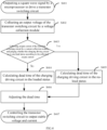
- FIG. 3 illustrates a flowchart of a dead time determination method according to an embodiment of the present disclosure. As illustrated in FIG. 3 , the method includes:
- the dead time thereof is calculated by the above Formula (2) according to the dead time y 1 of the charging driving circuit in the no-load status, the working frequency Fsw (the working frequency may be adjusted according to the output voltage using a Proportional Integration Differentiation (PID) adjustment mode) and the system clock frequency f , and then the transistor switching circuit can be controlled to output stable voltage and current according to the dead time of the charging driving circuit in the loaded status.
- PID Proportional Integration Differentiation
- the range of the system working frequency of the charging driving circuit may be 90K to 165K, and the range of the dead time may be 400 ns to 900 ns.
- the dead time determination method may also support the switching between the no-load status and the loaded status.
- FIG. 5 illustrates a schematic diagram of a computer device according to an embodiment of the present disclosure.
- the computer device 70 includes a memory 701, a processor 702, and a computer program which is stored in the memory 701 and executable in the processor 702, in which when executing the program, the processor 702 implements the aforementioned dead time determination method.
- the embodiments of the present disclosure further provide a computer-readable storage medium to solve the technical problem that the power device in the existing charging pile adopts a fixed dead time and requires a long charging time for charging the electric automobile.
- the computer-readable storage medium stores a computer program which performs the aforementioned dead time determination method.
- the charging driving circuit, the charging apparatus, the dead time determination method, the computer device and the computer-readable storage medium collect the output voltage of the transistor driving circuit by the voltage collection module and collect the output current of the transistor driving circuit by the current collection module, so that the micro-control unit can generate a control signal which controls the transistor switching circuit to be turned on or off according to the output voltage and the output current of the transistor switching circuit, and the transistor switching circuit can output a stable voltage to supply power to the load device.
- the charging driving circuit and the dead time determination method thereof can output stable voltage or current to the load device.
- These computer program instructions may also be loaded onto a computer or any other programmable data processing device, so that a series of operation steps can be performed on the computer or other programmable data processing device to produce a processing realized by the computer, thus the instructions executed on the computer or other programmable device provide step(s) for realizing function(s) specified in one or more flows in the flowchart and/or one or more blocks in the block diagram.
Landscapes
- Engineering & Computer Science (AREA)
- Power Engineering (AREA)
- Transportation (AREA)
- Mechanical Engineering (AREA)
- Charge And Discharge Circuits For Batteries Or The Like (AREA)
- Dc-Dc Converters (AREA)
- Secondary Cells (AREA)
Abstract
Description
- The present disclosure claims the priority of the Chinese patent application with an application number of
202110988747.2, an invention title of 'dead time determination method, charging driving circuit, apparatus, device and medium', and filed on August 26, 2021 - The present disclosure relates to the field of electric power, and particularly to a dead time determination method, a charging driving circuit, an apparatus, a device and a medium.
- This section is intended to provide a background or context for the embodiments of the present disclosure set forth in the claims. The description here is not admitted to be the prior art although it is included in this section.
- With the development of new energy automobiles, it is a new market demand to charge the new energy automobiles quickly. The existing charging piles often need a long charging duration to charge electric automobiles. In order to improve the charging efficiency of a power source, a power component in a bridge circuit should work in a soft switching state, so it is necessary to reasonably adjust the dead time corresponding to the power component.
- In the related art, fixed time control is usually adopted to control the dead time of the power component. However, when the dead time is controlled in this way in the related art, the dead time in some working areas may be shorter than actual soft switching time, which leads to insufficient soft switching and reduces the charging efficiency of the power source.
- The embodiments of the present disclosure provide a dead time determination method for determining dead time of a charging driving circuit in real time, including: acquiring output current of a charging driving circuit; determining a load status of the charging driving circuit according to the output current of the charging driving circuit; acquiring an output voltage of the charging driving circuit; and determining dead time of the charging driving circuit according to the output voltage and the load status of the charging driving circuit.
- Further, the load status is a no-load status or a loaded status.
- Further, determining the dead time y 1 of the charging driving circuit in the no-load status includes: calculating a product of a proportional coefficient k and an input voltage x; and calculating a sum of the product and a bias constant b, as the dead time y 1 of the charging driving circuit in the no-load status.
- Further, determining the dead time y of the charging driving circuit in the loaded status includes: calculating a product of a first coefficient and a ratio of a system clock frequency f to a working frequency; calculating a difference between the dead time y 1 of the charging driving circuit in the no-load status and the product; and calculating a product of the difference and a second coefficient, as the dead time y of the charging driving circuit in the loaded status.
- Further, determining the load status of the charging driving circuit according to the output current of the charging driving circuit includes: if the output current of the charging driving circuit is greater than a first preset threshold, determining the load status of the charging driving circuit as a loaded status; and if the output current of the charging driving circuit is less than a second preset threshold, determining the load status of the charging driving circuit as a no-load status.
- Further, the first preset threshold is greater than the second preset threshold.
- The embodiments of the present disclosure further provide a charging driving circuit to solve the technical problem that the power device in the existing charging pile adopts a fixed dead time and requires a long charging time for charging the electric automobile. The charging driving circuit includes: a power source module, a voltage collection module, a current collection module, a transistor driving circuit, a transistor switching circuit and a micro-control unit; in which the power source module is connected to a power source device and configured to provide a power supply voltage; the transistor switching circuit is connected to a load device and configured to supply power to the load device; the transistor driving circuit is connected between the micro-control unit and the transistor switching circuit, and configured to drive the transistor switching circuit to be turned on or off; the voltage collection module is connected to an output end of the transistor switching circuit and configured to collect an output voltage of the transistor switching circuit; the current collection module is connected to the output end of the transistor switching circuit and configured to collect output current of the transistor switching circuit; the micro-control unit is connected to the voltage collection module and the current collection module respectively, in which the micro-control unit is configured to determine dead time of the charging driving circuit according to the output voltage of the transistor switching circuit and the load status of the charging driving circuit, and generate a control signal that controls the transistor switching circuit to be turned on or off according to the dead time.
- Further, the transistor driving circuit is implemented by a first drive chip and a second drive chip, each being a dual-channel isolated gate driver with dual input interfaces to drive a half-bridge circuit or a full-bridge circuit.
- Further, the chip model used for the first drive chip and the second drive chip is UCC21520.
- Further, the micro-control unit includes: an acquisition unit configured to acquire the output voltage and the output current of the charging driving circuit; a judgement unit configured to judge a load status of the charging driving circuit according to the output current; and a calculation unit configured to calculate the dead time of the charging driving circuit according to the output voltage and the load status.
- The embodiments of the present disclosure further provide a charging apparatus to solve the technical problem that the power device in the existing charging pile adopts a fixed dead time and requires a long charging time for charging the electric automobile. The charging device includes: the aforementioned charging driving circuit.
- The embodiments of the present disclosure further provide a computer device to solve the technical problem that the power device in the existing charging pile adopts a fixed dead time and requires a long charging time for charging the electric automobile. The computer device includes a memory, a processor, and a computer program stored in the memory and executable in the processor, in which when executing the computer program, the processor implements the aforementioned dead time determination method.
- The embodiments of the present disclosure further provide a computer-readable storage medium to solve the technical problem that the power device in the existing charging pile adopts a fixed dead time and requires a long charging time for charging the electric automobile. The computer-readable storage medium stores a computer program which performs the aforementioned dead time determination method.
- According to the embodiments of the present disclosure, after the output current of the charging driving circuit is collected, the load status of the charging driving circuit is determined according to the output current of the charging driving circuit, and after the output voltage of the charging driving circuit is collected, the dead time of the charging driving circuit is determined according to the output voltage and the load status of the charging driving circuit, so as to obtain the dead time of the charging driving circuit in different load statuses, thereby ensuring sufficient soft switching, and then enabling the charging apparatus to output stable voltage or current.
- In order to more clearly explain the technical solutions in the embodiments of the present disclosure or in the prior art, the drawings to be used in the description of the embodiments or the prior art will be briefly introduced as follows. Obviously, the drawings concerned in the following description only illustrate some embodiments of the present disclosure, and those of ordinary skill in the art can obtain other drawings from them without paying any creative labor.
-
FIG. 1 illustrates a schematic diagram of a charging driving circuit according to an embodiment of the present disclosure; -
FIG. 2 illustrates a schematic diagram of a MOS driving circuit according to an embodiment of the present disclosure; -
FIG. 3 illustrates a flowchart of a dead time determination method according to an embodiment of the present disclosure; -
FIG. 4 illustrates a flowchart of a specific implementation of a dead time determination method according to an embodiment of the present disclosure; and -
FIG. 5 illustrates a schematic diagram of a computer device according to an embodiment of the present disclosure. - Reference signs:
- 10: power source module;
- 20: voltage collection module;
- 30: current collection module;
- 40: transistor driving circuit;
- 50: transistor switching circuit;
- 60: micro-control unit;
- 70: computer device;
- 701: memory;
- 702: processor.
- In order that the objectives, technical solutions and advantages of the embodiments of the present disclosure are clearer, the embodiments of the present disclosure will be further described in detail below with reference to the drawings. Here, the exemplary embodiments of the present disclosure and the description thereof are used to explain the present disclosure, rather than limitations thereto.
- An embodiment of the present disclosure provides a charging driving circuit, and
FIG. 1 illustrates a schematic diagram of a charging driving circuit according to an embodiment of the present disclosure. As illustrated inFIG. 1 , the charging driving circuit includes apower source module 10, avoltage collection module 20, acurrent collection module 30, atransistor driving circuit 40, atransistor switching circuit 50 and amicro-control unit 60; - in which the
power source module 10 is connected to a power source device and configured to provide a power supply voltage; - the
transistor switching circuit 50 is connected to a load device and configured to supply power to the load device; - the
transistor driving circuit 40 is connected between themicro-control unit 60 and thetransistor switching circuit 50, and configured to drive the transistor switching circuit to be turned on or off; - the
voltage collection module 20 is connected to an output end of thetransistor switching circuit 50 and configured to collect an output voltage of thetransistor switching circuit 50; - the
current collection module 30 is connected to the output end of thetransistor switching circuit 50 and configured to collect output current of thetransistor switching circuit 50; and - the
micro-control unit 60 is connected to thevoltage collection module 20 and thecurrent collection module 30 respectively, and configured to generate a control signal that controls thetransistor switching circuit 50 to be turned on or off according to the output voltage and the output current of thetransistor switching circuit 50. - During implementation, the
micro-control unit 60 may include an acquisition unit, a judgement unit and a calculation unit, in which the acquisition unit is configured to acquire the output voltage and the output current of the charging driving circuit; the judgement unit is configured to judge a load status of the charging driving circuit according to the output current; and the calculation unit is configured to calculate the dead time of the charging driving circuit according to the output voltage and the load status. - It should be noted that the control signal output by the
micro-control unit 60 may be a square wave signal, and high and low levels are output to control the transistor switching circuit to be turned on or off. When the transistor switching circuit is turned on, energy is transferred to a voltage output end, and an output voltage is regulated by controlling the time and speed of turning on the transistor switching circuit so as to output a stable DC voltage. - Since the Metal Oxide Semiconductor Field Effect Transistor (MOSFET) has the advantages of being smaller and more energy-saving, in an embodiment, the transistor according to the embodiments of the present disclosure adopts the MOSFET.
- In the charging driving circuit according to the embodiments of the present disclosure, the micro-control unit is implemented by a single chip microcomputer. In an embodiment, the microcontroller may adopt a chip with a model of TMS320F280049CPZS, the main frequency of which is 100 MHZ, which is powerful and has many on-chip analog peripherals.
- In order to be compatible with a half-bridge circuit and a full-bridge circuit, in an embodiment, in the charging driving circuit according to the embodiments of the present disclosure, the transistor driving circuit is implemented by a first drive chip and a second drive chip, each being a dual-channel isolated gate driver with dual input interfaces to drive the half-bridge circuit or the full-bridge circuit.
FIG. 2 illustrates a schematic diagram of a MOS driving circuit according to an embodiment of the present disclosure. U1 and U2 inFIG. 2 represent a first drive chip and a second drive chip, respectively. Herein the chip model used for the first drive chip and the second drive chip is UCC21520. - The UCC21520 is an isolated dual-channel gate driver with 4A peak source current and 6A peak sink current. The UCC21520 supports a high switching frequency and has a high isolation strength, and is configured to drive a Metal-Oxide-Semiconductor Field-Effect Transistor (MOSFET), an Insulated Gate Bipolar Transistor (IGBT), etc. Herein, each of the first drive chip and the second drive chip includes a drive part and a control part isolated from each other, and two internal drive channels isolated from each other.
- The embodiments of the present disclosure further provide a charging apparatus, which includes any one of the aforementioned charging driving circuits.
- It should be noted that the charging apparatus according to the embodiments of the present disclosure may be, but not limited to, a charging apparatus for an electric automobile.
- The embodiments of the present disclosure further provide a dead time determination method for determining dead time of a charging driving circuit in real time, and the dead time determination method may be used for, but not limited to, determining the dead time of the aforementioned charging driving circuit.
-
FIG. 3 illustrates a flowchart of a dead time determination method according to an embodiment of the present disclosure. As illustrated inFIG. 3 , the method includes: - S301: acquiring output current of a charging driving circuit;
- S302: determining a load status of the charging driving circuit according to the output current of the charging driving circuit;
- S303: acquiring an output voltage of the charging driving circuit; and
- S304: determining dead time of the charging driving circuit according to the output voltage and the load status of the charging driving circuit.
- It should be noted that the dead time in the embodiments of the present disclosure is a protection period set to prevent the upper and lower tubes of the full-bridge circuit or the half-bridge circuit from being turned on simultaneously due to the problem of the switching speed. The output current of the charging driving circuit is also the output current of the transistor switching circuit, and the output voltage of the charging driving circuit is also the output voltage of the transistor switching circuit. The load status of the charging driving circuit may be determined according to the output current of the charging driving circuit as follows: if the output current of the charging driving circuit is greater than a first preset threshold, determining the load status of the charging driving circuit as a loaded status; if the output current of the charging driving circuit is less than a second preset threshold, determining the load status of the charging driving circuit as a no-load status, in which the first preset threshold is greater than the second preset threshold, for example, the first preset threshold has a value range of 0.15A to 0.3A, and the second preset threshold has a value range of 0.05 A to 0.1A.
- In the embodiments of the present disclosure, the load status includes a no-load status or a loaded status.
- In the embodiments of the present disclosure, the no-load status refers to a state in which the charging driving circuit is connected to a load device but not charged; and the loaded status refers to a state in which the charging driving circuit is connected to the load device while being charged.
- In an embodiment, the dead time determination method according to the embodiments of the present disclosure may determine the dead time y 1 of the charging driving circuit in the no-load status by the following steps: calculating a first product of a proportional coefficient k and an input voltage x; and calculating a sum of the first product and a bias constant b, as the dead time y 1 of the charging driving circuit in the no-load status. In an embodiment, the dead time of the charging driving circuit in the no-load status is calculated by Formula (1).

where y 1 denotes the dead time of the charging driving circuit in the no-load status; k denotes a proportional coefficient representing a time unit; x denotes an input voltage; and b denotes a bias constant. - Further, the dead time determination method according to the embodiments of the present disclosure may determine the dead time y of the charging driving circuit in the loaded status by the following steps: calculating a second product of a first coefficient and a ratio of a system clock frequency f to a working frequency Fsw; calculating a difference between the dead time y 1 of the charging driving circuit in the no-load status and the second product; and calculating a product of the difference and a second coefficient as the dead time y of the charging driving circuit in the loaded status. In an embodiment, the dead time of the charging driving circuit in the loaded status is calculated by Formula (2), in which the first coefficient is equal to 0.3 and the second coefficient is equal to 10.

where y denotes the dead time of the charging driving circuit in the loaded status; f denotes a system clock frequency, which has a value range of 0 to 16 KHz; Fsw denotes a working frequency, which has a value range of 50 Hz to 60 Hz. -
FIG. 4 illustrates a flowchart of a specific implementation of a dead time determination method according to an embodiment of the present disclosure, including: - S401: outputting a square wave signal by a microprocessor to drive a transistor switching circuit;
- S402: collecting an output voltage of the transistor switching circuit by a voltage collection module;
- S403: collecting output current of the transistor switching circuit by a current collection module, and judging whether the charging driving circuit is in a no-load status according to the collected output current; if not, performing S404; and if so, performing S405;
- S404: calculating dead time of the charging driving circuit in the loaded status;
- S405: calculating dead time of the charging driving circuit in the no-load status;
- S406: adjusting the dead time;
- S407: controlling the transistor switching circuit to output stable voltage and current.
- It should be noted that when the charging driving circuit is in the no-load status, the dead time varies with the input voltage. The range of the input voltage may be 30 V to 400 V According to different input voltages, in order to make the charging driving circuit work in the soft switching area, the range of the working frequency of the system is adjusted and determined at first. For example, when the range of the no-load working frequency is 165 K, the range of the dead time is 1900 ns to 400 ns. The dead time of the charging driving circuit in the no-load status may be calculated by the above Formula (1). When the charging driving circuit is in the loaded status, the dead time thereof is calculated by the above Formula (2) according to the dead time y 1 of the charging driving circuit in the no-load status, the working frequency Fsw (the working frequency may be adjusted according to the output voltage using a Proportional Integration Differentiation (PID) adjustment mode) and the system clock frequency f, and then the transistor switching circuit can be controlled to output stable voltage and current according to the dead time of the charging driving circuit in the loaded status.
- It should be noted that depending on the output voltage and the output current, the range of the system working frequency of the charging driving circuit according to the embodiments of the present disclosure may be 90K to 165K, and the range of the dead time may be 400 ns to 900 ns.
- In order to make the whole system achieve a better working state and a higher efficiency to meet the customer requirements, in one embodiment, the dead time determination method according to the embodiments of the present disclosure may also support the switching between the no-load status and the loaded status.
- For example, in a case where the charging driving circuit works in the no-load status, when the output current of the transistor switching circuit is greater than a first preset threshold (e.g., 0.2A), the transistor switching circuit switches from the no-load status to the loaded status; and in a case where the charging driving circuit works in the loaded status, when the output current of the transistor switching circuit is less than a second preset threshold (e.g., 0.1A), the transistor switching circuit switches from the loaded status to the no-load status.
- Optionally, the load device in the embodiments of the present disclosure is a high-power load device. In a case where the load device is an electric automobile, the charging driving circuit according to the embodiments of the present disclosure may be disposed in a charging pile. The electric automobile can be rapidly and stably charged by disposing the charging driving circuit according to the embodiments of the present disclosure in the charging pile of the electric automobile. The charging driving circuit according to the embodiments of the present disclosure achieves a simple design, an easy replacement of components and a strong market competitiveness. The dead time determination method for the charging driving circuit according to the embodiments of the present disclosure is practical and simple.
- The embodiments of the present disclosure further provide a computer device to solve the technical problem that the power device in the existing charging pile adopts a fixed dead time and requires a long charging time for charging the electric automobile.
FIG. 5 illustrates a schematic diagram of a computer device according to an embodiment of the present disclosure. As illustrated inFIG. 5 , thecomputer device 70 includes amemory 701, aprocessor 702, and a computer program which is stored in thememory 701 and executable in theprocessor 702, in which when executing the program, theprocessor 702 implements the aforementioned dead time determination method. - The embodiments of the present disclosure further provide a computer-readable storage medium to solve the technical problem that the power device in the existing charging pile adopts a fixed dead time and requires a long charging time for charging the electric automobile. The computer-readable storage medium stores a computer program which performs the aforementioned dead time determination method.
- To sum up, the charging driving circuit, the charging apparatus, the dead time determination method, the computer device and the computer-readable storage medium according to the embodiments of the present disclosure collect the output voltage of the transistor driving circuit by the voltage collection module and collect the output current of the transistor driving circuit by the current collection module, so that the micro-control unit can generate a control signal which controls the transistor switching circuit to be turned on or off according to the output voltage and the output current of the transistor switching circuit, and the transistor switching circuit can output a stable voltage to supply power to the load device. According to the charging driving circuit and the dead time determination method thereof according to the embodiments of the present disclosure, the charging apparatus can output stable voltage or current to the load device.
- Those skilled in the art should appreciate that any embodiment of the present disclosure can be provided as a method, a system or a computer program product. Therefore, the present disclosure can take the form of a full hardware embodiment, a full software embodiment, or an embodiment combining software and hardware. Moreover, the present invention can take the form of a computer program product implemented on one or more computer usable storage mediums (including, but not limited to, a magnetic disc memory, CD-ROM, optical storage, etc.) containing therein computer usable program codes.
- The present disclosure is described with reference to a flowchart and/or a block diagram of the method, apparatus (system) and computer program product according to the embodiments of the present disclosure. It should be appreciated that each flow and/or block in the flowchart and/or the block diagram and a combination of flows and/or blocks in the flowchart and/or the block diagram can be realized by computer program instructions. Those computer program instructions can be provided to a general computer, a dedicated computer, an embedded processor or a processor of other programmable data processing device to produce a machine, so that the instructions executed by the processor of the computer or other programmable data processing device produce means for realizing specified functions in one or more flows in the flowchart and/or one or more blocks in the block diagram.
- These computer program instructions may also be stored in a computer readable memory capable of guiding the computer or other programmable data processing devices to work in a particular manner, so that the instructions stored in the computer readable memory can produce manufacture articles including an instructing device which realizes function(s) specified in one or more flows in the flowchart and/or one or more blocks in the block diagram.
- These computer program instructions may also be loaded onto a computer or any other programmable data processing device, so that a series of operation steps can be performed on the computer or other programmable data processing device to produce a processing realized by the computer, thus the instructions executed on the computer or other programmable device provide step(s) for realizing function(s) specified in one or more flows in the flowchart and/or one or more blocks in the block diagram.
- The specific embodiments described above further make detailed explanations to the objectives, technical solutions and advantageous effects of the present disclosure. It should be understood that those described above are only specific embodiments of the present disclosure and are not intended to limit the protection scope of the present disclosure. Any modification, equivalent substitution or improvement made within the spirit and principle of the present disclosure should fall within the protection scope of the present disclosure.
Claims (13)
- A dead time determination method for determining dead time of a charging driving circuit in real time, comprising:acquiring output current of a charging driving circuit;determining a load status of the charging driving circuit according to the output current of the charging driving circuit;acquiring an output voltage of the charging driving circuit; anddetermining dead time of the charging driving circuit according to the output voltage and the load status of the charging driving circuit.
- The dead time determination method according to claim 1, wherein the load status is a no-load status or a loaded status.
- The dead time determination method according to claim 2, wherein determining the dead time y 1 of the charging driving circuit in the no-load status comprises:calculating a product of a proportional coefficient k and an input voltage x; andcalculating a sum of the product and a bias constant b, as the dead time y 1 of the charging driving circuit in the no-load status.
- The dead time determination method according to claim 3, wherein determining the dead time y of the charging driving circuit in the loaded status comprises:calculating a product of a first coefficient and a ratio of a system clock frequency f to a working frequency;calculating a difference between the dead time y 1 of the charging driving circuit in the no-load status and the product; andcalculating a product of the difference and a second coefficient, as the dead time y of the charging driving circuit in the loaded status.
- The dead time determination method according to claim 1, wherein determining the load status of the charging driving circuit according to the output current of the charging driving circuit comprises:if the output current of the charging driving circuit is greater than a first preset threshold, determining the load status of the charging driving circuit as a loaded status; andif the output current of the charging driving circuit is less than a second preset threshold, determining the load status of the charging driving circuit as a no-load status.
- The dead time determination method according to claim 5, wherein the first preset threshold is greater than the second preset threshold.
- A charging driving circuit, comprising: a power source module, a voltage collection module, a current collection module, a transistor driving circuit, a transistor switching circuit and a micro-control unit;wherein the power source module is connected to a power source device and configured to provide a power supply voltage;the transistor switching circuit is connected to a load device and configured to supply power to the load device;the transistor driving circuit is connected between the micro-control unit and the transistor switching circuit, and configured to drive the transistor switching circuit to be turned on or off;the voltage collection module is connected to an output end of the transistor switching circuit and configured to collect an output voltage of the transistor switching circuit;the current collection module is connected to the output end of the transistor switching circuit and configured to collect output current of the transistor switching circuit;the micro-control unit is connected to the voltage collection module and the current collection module respectively, wherein the micro-control unit is configured to determine dead time of the charging driving circuit according to the output voltage of the transistor switching circuit and the load status of the charging driving circuit, and generate a control signal that controls the transistor switching circuit to be turned on or off according to the dead time.
- The charging driving circuit according to claim 7, wherein the transistor driving circuit is implemented by a first drive chip and a second drive chip, each being a dual-channel isolated gate driver with dual input interfaces to drive a half-bridge circuit or a full-bridge circuit.
- The charging driving circuit according to claim 8, wherein the chip model used for the first drive chip and the second drive chip is UCC21520.
- The charging driving circuit according to claim 7, wherein the micro-control unit comprises:an acquisition unit configured to acquire the output voltage and the output current of the charging driving circuit;a judgement unit configured to judge a load status of the charging driving circuit according to the output current; anda calculation unit configured to calculate the dead time of the charging driving circuit according to the output voltage and the load status.
- A charging apparatus, comprising the charging driving circuit according to any one of claims 7 to 10.
- A computer device, comprising a memory, a processor, and a computer program stored in the memory and executable in the processor, wherein when executing the computer program, the processor implements the dead time determination method according to any one of claims 1 to 6.
- A computer-readable storage medium, which stores a computer program which performs the dead time determination method according to any one of claims 1 to 6.
Applications Claiming Priority (2)
| Application Number | Priority Date | Filing Date | Title |
|---|---|---|---|
| CN202110988747.2A CN113690983B (en) | 2021-08-26 | 2021-08-26 | Dead time determination method, charging drive circuit, device, equipment and medium |
| PCT/CN2022/113854 WO2023025079A1 (en) | 2021-08-26 | 2022-08-22 | Dead time determination method, charging driving circuit and apparatus, and device and medium |
Publications (4)
| Publication Number | Publication Date |
|---|---|
| EP4395107A1 true EP4395107A1 (en) | 2024-07-03 |
| EP4395107A4 EP4395107A4 (en) | 2025-01-08 |
| EP4395107C0 EP4395107C0 (en) | 2026-01-28 |
| EP4395107B1 EP4395107B1 (en) | 2026-01-28 |
Family
ID=78583163
Family Applications (1)
| Application Number | Title | Priority Date | Filing Date |
|---|---|---|---|
| EP22860425.2A Active EP4395107B1 (en) | 2021-08-26 | 2022-08-22 | Dead time determination method, charging driving circuit and apparatus, and device and medium |
Country Status (7)
| Country | Link |
|---|---|
| US (1) | US20250132582A1 (en) |
| EP (1) | EP4395107B1 (en) |
| JP (1) | JP7743611B2 (en) |
| CN (1) | CN113690983B (en) |
| ES (1) | ES3063540T3 (en) |
| MX (1) | MX2024002480A (en) |
| WO (1) | WO2023025079A1 (en) |
Families Citing this family (1)
| Publication number | Priority date | Publication date | Assignee | Title |
|---|---|---|---|---|
| CN113690983B (en) * | 2021-08-26 | 2024-01-23 | 长春捷翼汽车科技股份有限公司 | Dead time determination method, charging drive circuit, device, equipment and medium |
Family Cites Families (16)
| Publication number | Priority date | Publication date | Assignee | Title |
|---|---|---|---|---|
| JP3482378B2 (en) * | 2000-06-01 | 2003-12-22 | 松下電器産業株式会社 | Switching power supply |
| JP3942583B2 (en) * | 2003-11-21 | 2007-07-11 | 松下電器産業株式会社 | Driver circuit |
| CN102723872B (en) * | 2011-03-29 | 2014-09-03 | 华为技术有限公司 | Power supply apparatus and method for adjusting dead time |
| CN103001577B (en) * | 2011-09-09 | 2015-03-25 | 台达电子工业股份有限公司 | Driver with dead-zone open circuit compensation |
| CN103887982B (en) * | 2014-03-21 | 2017-11-03 | 许继电气股份有限公司 | ZVS control method in a kind of digital LLC |
| JP5866614B1 (en) | 2014-12-05 | 2016-02-17 | パナソニックIpマネジメント株式会社 | Switching power supply |
| CN104578341B (en) * | 2014-12-29 | 2017-01-25 | 东南大学 | An on-board charger with adjustable dead time based on phase-shifted full-bridge circuit |
| CN105763051B (en) * | 2016-04-14 | 2019-01-25 | 中国科学院上海微系统与信息技术研究所 | A light-load frequency reduction mode control system |
| CN105978123B (en) * | 2016-06-06 | 2018-05-15 | 东南大学 | A kind of dynamic adjusting system of phase-shifting full-bridge formula Vehicular charger dead time |
| US10181782B2 (en) | 2017-04-18 | 2019-01-15 | Richtek Technology Corporation | Flyback power converter circuit with active clamping and zero voltage switching and conversion control circuit thereof |
| CN110277919A (en) * | 2018-03-15 | 2019-09-24 | 联合汽车电子有限公司 | A kind of method of real-time dead time of the amendment DC/DC converter under Sofe Switch |
| CN108471227A (en) * | 2018-04-12 | 2018-08-31 | 四川升华电源科技有限公司 | A kind of power inverter control method and device |
| JP6979981B2 (en) | 2019-05-16 | 2021-12-15 | コーセル株式会社 | Switching power supply |
| CN111900944A (en) * | 2020-07-27 | 2020-11-06 | 张金路 | Composite parallel connection type audio digital power amplifier without dead zone distortion |
| CN112994472B (en) * | 2021-04-12 | 2022-06-14 | 华中科技大学 | Optimal dead zone calculation method and variable dead zone control method for high-frequency LLC resonant converter |
| CN113690983B (en) * | 2021-08-26 | 2024-01-23 | 长春捷翼汽车科技股份有限公司 | Dead time determination method, charging drive circuit, device, equipment and medium |
-
2021
- 2021-08-26 CN CN202110988747.2A patent/CN113690983B/en active Active
-
2022
- 2022-08-22 WO PCT/CN2022/113854 patent/WO2023025079A1/en not_active Ceased
- 2022-08-22 ES ES22860425T patent/ES3063540T3/en active Active
- 2022-08-22 EP EP22860425.2A patent/EP4395107B1/en active Active
- 2022-08-22 US US18/686,774 patent/US20250132582A1/en active Pending
- 2022-08-22 MX MX2024002480A patent/MX2024002480A/en unknown
- 2022-08-22 JP JP2024513155A patent/JP7743611B2/en active Active
Also Published As
| Publication number | Publication date |
|---|---|
| CN113690983B (en) | 2024-01-23 |
| EP4395107A4 (en) | 2025-01-08 |
| CN113690983A (en) | 2021-11-23 |
| ES3063540T3 (en) | 2026-04-17 |
| EP4395107C0 (en) | 2026-01-28 |
| EP4395107B1 (en) | 2026-01-28 |
| JP2024529783A (en) | 2024-08-08 |
| WO2023025079A1 (en) | 2023-03-02 |
| MX2024002480A (en) | 2024-04-23 |
| US20250132582A1 (en) | 2025-04-24 |
| JP7743611B2 (en) | 2025-09-24 |
Similar Documents
| Publication | Publication Date | Title |
|---|---|---|
| US11223290B2 (en) | Power conversion device, control method, and computer-readable medium | |
| US6765371B2 (en) | Non-isolated DC-DC converter for performing direct current power conversion | |
| JP4496988B2 (en) | Gate drive circuit | |
| EP2228882A2 (en) | Charging control device and method, charging device, as well as, program | |
| US20110095711A1 (en) | Single-stage zero-current switching driving circuit for ultrasonic motor | |
| CN113765341A (en) | A driver, motor drive circuit and power system | |
| EP4395107B1 (en) | Dead time determination method, charging driving circuit and apparatus, and device and medium | |
| KR20170064080A (en) | Charging control method and system of high voltage battery for vehicle | |
| EP1883153A2 (en) | Inverter | |
| CN1544955A (en) | Comprehensive test instrument of electric system primary cut out | |
| EP2146424A2 (en) | Alternating-current power supply device recovering magnetic energy | |
| JP2016226152A (en) | Power control device | |
| US11984830B2 (en) | Inverter with switch control and a method of controlling an inverter | |
| US20210344268A1 (en) | Driving apparatus and driving method for semiconductor switch, power conversion apparatus, and vehicle | |
| CN119341362B (en) | Power conversion equipment and its control methods, switch driver chips | |
| US8378729B2 (en) | Signal control device | |
| CN112491252A (en) | Driving method and circuit for improving reliability of SIC MOSFET | |
| KR100427320B1 (en) | Auxiliary Source providing System using Main Battery | |
| US11658563B2 (en) | Half-bridge power supply with dynamic dead time | |
| CN108390553B (en) | Compensation method for motor transmission PWM dead zone | |
| KR101947858B1 (en) | Control method and system of converter | |
| US12074550B2 (en) | Control device, inverter, assembly having an inverter and an electrical machine, method for operating an inverter, and computer program | |
| KR101043403B1 (en) | Power supply and power supply method | |
| US20230238874A1 (en) | Isolated resonant conversion control method, apparatus and system, and readable storage medium | |
| JP2000060004A (en) | Battery charger for electric rolling stock |
Legal Events
| Date | Code | Title | Description |
|---|---|---|---|
| STAA | Information on the status of an ep patent application or granted ep patent |
Free format text: STATUS: THE INTERNATIONAL PUBLICATION HAS BEEN MADE |
|
| PUAI | Public reference made under article 153(3) epc to a published international application that has entered the european phase |
Free format text: ORIGINAL CODE: 0009012 |
|
| STAA | Information on the status of an ep patent application or granted ep patent |
Free format text: STATUS: REQUEST FOR EXAMINATION WAS MADE |
|
| 17P | Request for examination filed |
Effective date: 20240325 |
|
| AK | Designated contracting states |
Kind code of ref document: A1 Designated state(s): AL AT BE BG CH CY CZ DE DK EE ES FI FR GB GR HR HU IE IS IT LI LT LU LV MC MK MT NL NO PL PT RO RS SE SI SK SM TR |
|
| P01 | Opt-out of the competence of the unified patent court (upc) registered |
Free format text: CASE NUMBER: APP_43247/2024 Effective date: 20240724 |
|
| DAV | Request for validation of the european patent (deleted) | ||
| DAX | Request for extension of the european patent (deleted) | ||
| A4 | Supplementary search report drawn up and despatched |
Effective date: 20241205 |
|
| RIC1 | Information provided on ipc code assigned before grant |
Ipc: H02M 1/38 20070101ALI20241129BHEP Ipc: H02M 1/08 20060101ALI20241129BHEP Ipc: B60L 53/62 20190101ALI20241129BHEP Ipc: H02J 7/00 20060101AFI20241129BHEP |
|
| GRAP | Despatch of communication of intention to grant a patent |
Free format text: ORIGINAL CODE: EPIDOSNIGR1 |
|
| STAA | Information on the status of an ep patent application or granted ep patent |
Free format text: STATUS: GRANT OF PATENT IS INTENDED |
|
| INTG | Intention to grant announced |
Effective date: 20250910 |
|
| GRAS | Grant fee paid |
Free format text: ORIGINAL CODE: EPIDOSNIGR3 |
|
| GRAA | (expected) grant |
Free format text: ORIGINAL CODE: 0009210 |
|
| STAA | Information on the status of an ep patent application or granted ep patent |
Free format text: STATUS: THE PATENT HAS BEEN GRANTED |
|
| AK | Designated contracting states |
Kind code of ref document: B1 Designated state(s): AL AT BE BG CH CY CZ DE DK EE ES FI FR GB GR HR HU IE IS IT LI LT LU LV MC MK MT NL NO PL PT RO RS SE SI SK SM TR |
|
| REG | Reference to a national code |
Ref country code: CH Ref legal event code: F10 Free format text: ST27 STATUS EVENT CODE: U-0-0-F10-F00 (AS PROVIDED BY THE NATIONAL OFFICE) Effective date: 20260128 Ref country code: GB Ref legal event code: FG4D |
|
| REG | Reference to a national code |
Ref country code: DE Ref legal event code: R096 Ref document number: 602022029498 Country of ref document: DE |
|
| REG | Reference to a national code |
Ref country code: IE Ref legal event code: FG4D |
|
| U01 | Request for unitary effect filed |
Effective date: 20260212 |
|
| P04 | Withdrawal of opt-out of the competence of the unified patent court (upc) registered |
Free format text: CASE NUMBER: APP_43247_1/2024 Effective date: 20260218 |
|
| U07 | Unitary effect registered |
Designated state(s): AT BE BG DE DK EE FI FR IT LT LU LV MT NL PT RO SE SI Effective date: 20260218 |
|
| REG | Reference to a national code |
Ref country code: ES Ref legal event code: FG2A Ref document number: 3063540 Country of ref document: ES Kind code of ref document: T3 Effective date: 20260417 |