EP4395048A1 - Electrochemical device and electronic device - Google Patents
Electrochemical device and electronic device Download PDFInfo
- Publication number
- EP4395048A1 EP4395048A1 EP21966704.5A EP21966704A EP4395048A1 EP 4395048 A1 EP4395048 A1 EP 4395048A1 EP 21966704 A EP21966704 A EP 21966704A EP 4395048 A1 EP4395048 A1 EP 4395048A1
- Authority
- EP
- European Patent Office
- Prior art keywords
- region
- layer
- electrochemical apparatus
- conductive
- conductive material
- Prior art date
- Legal status (The legal status is an assumption and is not a legal conclusion. Google has not performed a legal analysis and makes no representation as to the accuracy of the status listed.)
- Granted
Links
Images









Classifications
-
- H—ELECTRICITY
- H01—ELECTRIC ELEMENTS
- H01M—PROCESSES OR MEANS, e.g. BATTERIES, FOR THE DIRECT CONVERSION OF CHEMICAL ENERGY INTO ELECTRICAL ENERGY
- H01M4/00—Electrodes
- H01M4/02—Electrodes composed of, or comprising, active material
- H01M4/13—Electrodes for accumulators with non-aqueous electrolyte, e.g. for lithium-accumulators; Processes of manufacture thereof
-
- H—ELECTRICITY
- H01—ELECTRIC ELEMENTS
- H01M—PROCESSES OR MEANS, e.g. BATTERIES, FOR THE DIRECT CONVERSION OF CHEMICAL ENERGY INTO ELECTRICAL ENERGY
- H01M10/00—Secondary cells; Manufacture thereof
- H01M10/04—Construction or manufacture in general
-
- H—ELECTRICITY
- H01—ELECTRIC ELEMENTS
- H01M—PROCESSES OR MEANS, e.g. BATTERIES, FOR THE DIRECT CONVERSION OF CHEMICAL ENERGY INTO ELECTRICAL ENERGY
- H01M10/00—Secondary cells; Manufacture thereof
- H01M10/04—Construction or manufacture in general
- H01M10/0431—Cells with wound or folded electrodes
-
- H—ELECTRICITY
- H01—ELECTRIC ELEMENTS
- H01M—PROCESSES OR MEANS, e.g. BATTERIES, FOR THE DIRECT CONVERSION OF CHEMICAL ENERGY INTO ELECTRICAL ENERGY
- H01M10/00—Secondary cells; Manufacture thereof
- H01M10/05—Accumulators with non-aqueous electrolyte
- H01M10/052—Li-accumulators
- H01M10/0525—Rocking-chair batteries, i.e. batteries with lithium insertion or intercalation in both electrodes; Lithium-ion batteries
-
- H—ELECTRICITY
- H01—ELECTRIC ELEMENTS
- H01M—PROCESSES OR MEANS, e.g. BATTERIES, FOR THE DIRECT CONVERSION OF CHEMICAL ENERGY INTO ELECTRICAL ENERGY
- H01M10/00—Secondary cells; Manufacture thereof
- H01M10/05—Accumulators with non-aqueous electrolyte
- H01M10/058—Construction or manufacture
- H01M10/0587—Construction or manufacture of accumulators having only wound construction elements, i.e. wound positive electrodes, wound negative electrodes and wound separators
-
- H—ELECTRICITY
- H01—ELECTRIC ELEMENTS
- H01M—PROCESSES OR MEANS, e.g. BATTERIES, FOR THE DIRECT CONVERSION OF CHEMICAL ENERGY INTO ELECTRICAL ENERGY
- H01M10/00—Secondary cells; Manufacture thereof
- H01M10/60—Heating or cooling; Temperature control
- H01M10/61—Types of temperature control
- H01M10/613—Cooling or keeping cold
-
- H—ELECTRICITY
- H01—ELECTRIC ELEMENTS
- H01M—PROCESSES OR MEANS, e.g. BATTERIES, FOR THE DIRECT CONVERSION OF CHEMICAL ENERGY INTO ELECTRICAL ENERGY
- H01M10/00—Secondary cells; Manufacture thereof
- H01M10/60—Heating or cooling; Temperature control
- H01M10/65—Means for temperature control structurally associated with the cells
- H01M10/654—Means for temperature control structurally associated with the cells located inside the innermost case of the cells, e.g. mandrels, electrodes or electrolytes
-
- H—ELECTRICITY
- H01—ELECTRIC ELEMENTS
- H01M—PROCESSES OR MEANS, e.g. BATTERIES, FOR THE DIRECT CONVERSION OF CHEMICAL ENERGY INTO ELECTRICAL ENERGY
- H01M50/00—Constructional details or processes of manufacture of the non-active parts of electrochemical cells other than fuel cells, e.g. hybrid cells
- H01M50/10—Primary casings; Jackets or wrappings
- H01M50/102—Primary casings; Jackets or wrappings characterised by their shape or physical structure
- H01M50/105—Pouches or flexible bags
-
- H—ELECTRICITY
- H01—ELECTRIC ELEMENTS
- H01M—PROCESSES OR MEANS, e.g. BATTERIES, FOR THE DIRECT CONVERSION OF CHEMICAL ENERGY INTO ELECTRICAL ENERGY
- H01M50/00—Constructional details or processes of manufacture of the non-active parts of electrochemical cells other than fuel cells, e.g. hybrid cells
- H01M50/10—Primary casings; Jackets or wrappings
- H01M50/172—Arrangements of electric connectors penetrating the casing
- H01M50/174—Arrangements of electric connectors penetrating the casing adapted for the shape of the cells
- H01M50/178—Arrangements of electric connectors penetrating the casing adapted for the shape of the cells for pouch or flexible bag cells
-
- H—ELECTRICITY
- H01—ELECTRIC ELEMENTS
- H01M—PROCESSES OR MEANS, e.g. BATTERIES, FOR THE DIRECT CONVERSION OF CHEMICAL ENERGY INTO ELECTRICAL ENERGY
- H01M50/00—Constructional details or processes of manufacture of the non-active parts of electrochemical cells other than fuel cells, e.g. hybrid cells
- H01M50/10—Primary casings; Jackets or wrappings
- H01M50/183—Sealing members
- H01M50/19—Sealing members characterised by the material
- H01M50/193—Organic material
-
- H—ELECTRICITY
- H01—ELECTRIC ELEMENTS
- H01M—PROCESSES OR MEANS, e.g. BATTERIES, FOR THE DIRECT CONVERSION OF CHEMICAL ENERGY INTO ELECTRICAL ENERGY
- H01M50/00—Constructional details or processes of manufacture of the non-active parts of electrochemical cells other than fuel cells, e.g. hybrid cells
- H01M50/40—Separators; Membranes; Diaphragms; Spacing elements inside cells
- H01M50/46—Separators, membranes or diaphragms characterised by their combination with electrodes
-
- H—ELECTRICITY
- H01—ELECTRIC ELEMENTS
- H01M—PROCESSES OR MEANS, e.g. BATTERIES, FOR THE DIRECT CONVERSION OF CHEMICAL ENERGY INTO ELECTRICAL ENERGY
- H01M50/00—Constructional details or processes of manufacture of the non-active parts of electrochemical cells other than fuel cells, e.g. hybrid cells
- H01M50/50—Current conducting connections for cells or batteries
- H01M50/531—Electrode connections inside a battery casing
-
- H—ELECTRICITY
- H01—ELECTRIC ELEMENTS
- H01M—PROCESSES OR MEANS, e.g. BATTERIES, FOR THE DIRECT CONVERSION OF CHEMICAL ENERGY INTO ELECTRICAL ENERGY
- H01M50/00—Constructional details or processes of manufacture of the non-active parts of electrochemical cells other than fuel cells, e.g. hybrid cells
- H01M50/50—Current conducting connections for cells or batteries
- H01M50/531—Electrode connections inside a battery casing
- H01M50/533—Electrode connections inside a battery casing characterised by the shape of the leads or tabs
-
- H—ELECTRICITY
- H01—ELECTRIC ELEMENTS
- H01M—PROCESSES OR MEANS, e.g. BATTERIES, FOR THE DIRECT CONVERSION OF CHEMICAL ENERGY INTO ELECTRICAL ENERGY
- H01M50/00—Constructional details or processes of manufacture of the non-active parts of electrochemical cells other than fuel cells, e.g. hybrid cells
- H01M50/50—Current conducting connections for cells or batteries
- H01M50/531—Electrode connections inside a battery casing
- H01M50/536—Electrode connections inside a battery casing characterised by the method of fixing the leads to the electrodes, e.g. by welding
-
- H—ELECTRICITY
- H01—ELECTRIC ELEMENTS
- H01M—PROCESSES OR MEANS, e.g. BATTERIES, FOR THE DIRECT CONVERSION OF CHEMICAL ENERGY INTO ELECTRICAL ENERGY
- H01M50/00—Constructional details or processes of manufacture of the non-active parts of electrochemical cells other than fuel cells, e.g. hybrid cells
- H01M50/50—Current conducting connections for cells or batteries
- H01M50/531—Electrode connections inside a battery casing
- H01M50/538—Connection of several leads or tabs of wound or folded electrode stacks
-
- H—ELECTRICITY
- H01—ELECTRIC ELEMENTS
- H01M—PROCESSES OR MEANS, e.g. BATTERIES, FOR THE DIRECT CONVERSION OF CHEMICAL ENERGY INTO ELECTRICAL ENERGY
- H01M50/00—Constructional details or processes of manufacture of the non-active parts of electrochemical cells other than fuel cells, e.g. hybrid cells
- H01M50/50—Current conducting connections for cells or batteries
- H01M50/572—Means for preventing undesired use or discharge
- H01M50/584—Means for preventing undesired use or discharge for preventing incorrect connections inside or outside the batteries
- H01M50/59—Means for preventing undesired use or discharge for preventing incorrect connections inside or outside the batteries characterised by the protection means
- H01M50/593—Spacers; Insulating plates
-
- H—ELECTRICITY
- H01—ELECTRIC ELEMENTS
- H01M—PROCESSES OR MEANS, e.g. BATTERIES, FOR THE DIRECT CONVERSION OF CHEMICAL ENERGY INTO ELECTRICAL ENERGY
- H01M50/00—Constructional details or processes of manufacture of the non-active parts of electrochemical cells other than fuel cells, e.g. hybrid cells
- H01M50/50—Current conducting connections for cells or batteries
- H01M50/572—Means for preventing undesired use or discharge
- H01M50/584—Means for preventing undesired use or discharge for preventing incorrect connections inside or outside the batteries
- H01M50/59—Means for preventing undesired use or discharge for preventing incorrect connections inside or outside the batteries characterised by the protection means
- H01M50/597—Protection against reversal of polarity
-
- H—ELECTRICITY
- H01—ELECTRIC ELEMENTS
- H01M—PROCESSES OR MEANS, e.g. BATTERIES, FOR THE DIRECT CONVERSION OF CHEMICAL ENERGY INTO ELECTRICAL ENERGY
- H01M4/00—Electrodes
- H01M4/02—Electrodes composed of, or comprising, active material
- H01M2004/021—Physical characteristics, e.g. porosity, surface area
-
- Y—GENERAL TAGGING OF NEW TECHNOLOGICAL DEVELOPMENTS; GENERAL TAGGING OF CROSS-SECTIONAL TECHNOLOGIES SPANNING OVER SEVERAL SECTIONS OF THE IPC; TECHNICAL SUBJECTS COVERED BY FORMER USPC CROSS-REFERENCE ART COLLECTIONS [XRACs] AND DIGESTS
- Y02—TECHNOLOGIES OR APPLICATIONS FOR MITIGATION OR ADAPTATION AGAINST CLIMATE CHANGE
- Y02E—REDUCTION OF GREENHOUSE GAS [GHG] EMISSIONS, RELATED TO ENERGY GENERATION, TRANSMISSION OR DISTRIBUTION
- Y02E60/00—Enabling technologies; Technologies with a potential or indirect contribution to GHG emissions mitigation
- Y02E60/10—Energy storage using batteries
-
- Y—GENERAL TAGGING OF NEW TECHNOLOGICAL DEVELOPMENTS; GENERAL TAGGING OF CROSS-SECTIONAL TECHNOLOGIES SPANNING OVER SEVERAL SECTIONS OF THE IPC; TECHNICAL SUBJECTS COVERED BY FORMER USPC CROSS-REFERENCE ART COLLECTIONS [XRACs] AND DIGESTS
- Y02—TECHNOLOGIES OR APPLICATIONS FOR MITIGATION OR ADAPTATION AGAINST CLIMATE CHANGE
- Y02P—CLIMATE CHANGE MITIGATION TECHNOLOGIES IN THE PRODUCTION OR PROCESSING OF GOODS
- Y02P70/00—Climate change mitigation technologies in the production process for final industrial or consumer products
- Y02P70/50—Manufacturing or production processes characterised by the final manufactured product
Definitions
- Electrochemical apparatuses for example, batteries
- electronic products such as electronic mobile devices, electric tools, and electric vehicles, and increasingly high requirements are imposed on safety performance of the electrochemical apparatuses.
- an electrochemical apparatus During high-rate charging, an electrochemical apparatus is likely to continuously produce heat and have a temperature rise due to factors such as its internal resistance and polarization accumulation caused by charging. This may accelerate aging of the electrochemical apparatus as well as deterioration of capacity and power performance, and may also cause volumetric expansion, deformation, or the like, affecting the service life of a product.
- the electrode assembly is of a wound structure and includes a first electrode plate.
- the first electrode plate includes a first conductive layer and a first conductive material layer.
- the first conductive layer includes a first surface and a second surface opposite to each other.
- the first conductive material layer is provided on the first surface.
- the first surface includes a first region, the first conductive material layer includes a first recess, and the first region is exposed from the first recess.
- the first conductive plate is connected to the first region and extends out of the first electrode plate.
- the first conductive plate includes a third region and a fourth region connected to each other.
- a direction perpendicular to the third region is a first direction, and in the first direction, a projection of the third region is located in a projection of the first region, and a projection of the fourth region is located outside the projection of the first region.
- the third region includes a connection region, and the first conductive plate is connected to the first region through the connection region. Viewed from the first direction, the third region includes a first side, a second side, a third side, and a fourth side, the first side and the second side being opposite to each other, the third side and the fourth side being opposite to each other, and the fourth side being connected to the fourth region.
- the first region includes a fifth side, a sixth side, and a seventh side.
- An extension direction of the third region is a second direction, and in the second direction, the seventh side and the third side are arranged in sequence.
- the fifth side, the first side, the second side, and the sixth side are arranged in sequence.
- the first direction, the second direction, and the third direction are perpendicular to each other.
- a size of the third region in the third direction is T 1
- a size of the third region in the second direction is T 2
- an area of the projection of the third region in the first direction is S 1
- an area of a projection of the connection region in the first direction is S 2
- a distance between the first side and the fifth side is J 1
- a distance between the second side and the sixth side is J 2
- a distance between the third side and the seventh side is J 3 , where S 2 /S 1 + (J 1 + J 2 + J 3 )/(T 1 + T 2 ) ⁇ 30%.
- the first electrode plate further includes a second conductive material layer provided on the second surface.
- the second surface includes a second region, the second conductive material layer includes a second recess, and the second region is exposed from the second recess.
- the projection of the first region and a projection of the second region at least partially overlap.
- the electrochemical apparatus further includes a first layer adhered to the third region, where the first layer contains an insulating material.
- the projection of the third region is located in a projection of the first layer.
- the first layer may reduce the risk of generation of a short circuit caused when a burr or welding mark of the connection region punctures a separator, and may also be configured to compensate for a reduced thickness of a position where the first recess is provided on the first conductive material layer, allowing the electrochemical apparatus to have a more uniform overall thickness.
- the first conductive material layer includes a first conductive material region, where the first conductive material region encloses the first recess.
- the first layer is further adhered to the first conductive material region. In the first direction, the projection of the first region is located in the projection of the first layer.
- the electrochemical apparatus further includes a second layer, where the second layer contains an insulating material.
- the second conductive material layer includes a second conductive material region, where the second conductive material region encloses the second recess.
- the second layer is adhered to the second conductive material region. In the first direction, the projection of the second region is located in a projection of the second layer.
- the second layer may be configured to compensate for a reduced thickness of a position where the second recess is provided on the second conductive material layer.
- a third recess is provided at an edge of the first region in the second direction.
- the first conductive material region includes a first extension region and a second extension region extending toward the third recess. Viewed in the first direction, the first extension region and the second extension region are disposed on two sides of the third recess.
- a distance between an edge of the first region in the second direction and the eighth side is L 1
- the first extension region and the second extension region have a same size of L 2 in the second direction
- a distance between the seventh side and the eighth side is L 3 , where (L 2 + L 3 )/L 1 ⁇ 30%.
- a size of the first extension region in the third direction is W 1
- a size of the second extension region in the third direction is W 2 , where (W 1 + W 2 )/T 1 ⁇ 20%.
- a size of the first extension region in the third direction is W 1
- a size of the second extension region in the third direction is W 2
- a distance between the first extension region and the first conductive plate in the third direction is W 3
- a distance between the second extension region and the first conductive plate in the third direction is W 4 .
- W 3 ⁇ W 1
- W 2 ⁇ W 4
- W 3 ⁇ W 4 .
- the first extension region and/or the second extension region has a size of L 2 , and a distance between the ninth side and the fourth side is L 4 , where L 2 ⁇ L 4 .
- the relatively large L 4 helps to further increase the heat dissipation area of the first conductive plate, thereby reducing a temperature rise during large-current charging.
- L 1 ranges from 10 mm to 50 mm.
- the first conductive material layer covered by the first layer in the second direction has a relatively large size, and therefore has a greater impact on the capacity of the electrochemical apparatus.
- the first region also has a small size in the second direction, so that the distance J 3 between the third side and the seventh side is also small, and thus heat dissipation capability of the first region is also reduced.
- the third layer may also be configured to hinder movement, toward the second recess, of lithium ions deintercalated from a part of the third conductive material layer corresponding to the third layer in the first direction, thereby reducing the risks of excessive accumulation of lithium ions and formation of lithium dendrites due to the lack of lithium ions that may be embedded in the second recess.
- the fourth layer may also reduce the risk of formation of lithium dendrites.
- an edge of at least one of the first layer or the second layer extends beyond an edge of the first electrode plate.
- the electrode assembly further includes a second electrode plate and a separator.
- the first electrode plate, the separator, and the second electrode plate are stacked and wound to form the electrode assembly.
- the electrode assembly includes a first section, a first bent section, a second section, and a second bent section connected in sequence.
- the first conductive plate is located in the first section, thereby improving the flatness of the first conductive plate when the first conductive plate is connected to the first region.
- the fourth direction D 4 is a direction from a first winding start end 21a to a first winding stop end 21b of the first electrode plate 21, and also a direction from a second winding start end 22a to a second winding stop end 22b of the second electrode plate 22.
- the electrode assembly 20 in the winding direction D, includes a first section 201, a first bent section 202, a second section 203, and a second bent section 204 that are connected in sequence.
- the first direction D 1 is a direction in which the first electrode plate 21 in the first section 201 or second section 203 is stacked.
- the electrode assembly 20 may include a plurality of first sections 201, a plurality of first bent sections 202, a plurality of second sections 203, and a plurality of second bent sections 204.
- the first section 201 and the second section 203 may be flat and straight sections.
- the electrode assembly 20 in the winding direction D, may alternatively include four bent sections that are connected in sequence.
- a joint between the outermost first bent section 202 of the electrode assembly 20 and the outermost second section 203 of the electrode assembly 20 is a second end 206.
- the second end 206 is a stop portion of the rightmost bent side of the first bent section 202 in FIG. 3A in the winding direction D, and the second end 206 is also a portion where the dotted line B-B formed by extension, of the innermost bent side at the right in the electrode assembly 10, in the first direction D 1 is intersected with the second outer surface 203a.
- a joint between the outermost second section 203 of the electrode assembly 20 and the outermost second bent section 204 of the electrode assembly 20 is a third end 207.
- the third end 207 is a start portion of a leftmost curve of the second bent section 204 in FIG.
- the fourth end 208 is also a portion where the dotted line A-A formed by extension, of the innermost bent side at the left in the electrode assembly 10, in the first direction D 1 is intersected with the first outer surface 201a.
- the first end 205 and the second end 206 are aligned, and the third end 207 and the fourth end 208 are aligned.
- the positive electrode active material layer includes a positive electrode active material, and the positive electrode active material includes a compound that reversibly intercalates and deintercalates lithium ions (that is, a lithiated intercalation compound).
- the positive electrode active material may include a lithium transition metal composite oxide.
- the lithium transition metal composite oxide contains lithium and at least one element selected from cobalt, manganese, and nickel.
- the separator 23 includes at least one of polyethylene, polypropylene, polyvinylidene fluoride, polyethylene terephthalate, polyimide, or aramid.
- polyethylene is selected from at least one of high-density polyethylene, low-density polyethylene, or ultrahigh-molecular-weight polyethylene.
- Polyethylene and polypropylene have a good effect on alleviating short circuits and may improve the stability of a battery through a shutdown effect.
- the first surface 210a of the first conductive layer 210 includes a first region 2100.
- the first conductive material layer 211 includes a first recess 2110.
- the first recess 2110 may be formed by opening a first end edge 211a of the first conductive material layer 211 inward in a direction of the winding center axis C, and the first recess 2110 does not run through a second end edge 211b of the first conductive material layer 211 in the direction of the winding center axis C.
- the first region 2100 is exposed from the first recess 2110, and the first region 2100 is separated from the first conductive material layer 211.
- the first recess 2110 may be formed by laser cleaning in the first conductive material layer 211 so that the first region 2100 is exposed.
- the first region 2100 may be bonded with polystyrene foam, coated with an active material, and then heated to make the polystyrene foam fall off, so that the first region 2100 is exposed.
- the active material on the first region 2100 may be directly scraped using a scraper, so that the first region 2100 is exposed.
- a scraper so that after laser cleaning or scraping using a scraper, there is still a small amount of active material on the surface of the first region 2100. This is not limited in this application.
- the first conductive plate 30 is connected to the first region 2100 and extends out of the first region 2100 and beyond the first end edge 211a from the first region 2100, allowing for a connection to an external component (not shown in the figure).
- the first region 2100 may be disposed in an area other than a winding head and a winding tail of the first electrode plate 21.
- the projections of the first region 2100 and the first recess 2110 in the first direction D 1 may both be rectangular. In some specific embodiments, the projections of the first region 2100 and the first recess 2110 in the first direction D 1 are both rectangular.
- the third wall 113 is disposed between the first wall 111 and the second wall 112, and the fourth wall 114 is also disposed between the first wall 111 and the second wall 112.
- the first conductive plate 30 and the second conductive plate 40 respectively extend out of the sealing edge 12 from the inside of the housing 10 to the outside of the housing 10.
- the housing 10 includes a first housing 13 and a second housing 14 opposite to each other.
- the housing 10 may be formed by heat-sealing the first housing 13 and the second housing 14.
- the first housing 13 is provided with a first space 130
- the second housing 14 is a flat plate structure.
- the first space 130 is enclosed by the second housing 14 to form an accommodating space for accommodating the electrode assembly 20.
- the first housing 14 may also have a second space (not shown in the figure). After the first housing 13 and the second housing 14 are heat-sealed, the first space 130 and the second space cooperate with each other to form an accommodating space for accommodating the electrode assembly 20.
- a distance W 4 from the first conductive plate 30 to the second lateral side R 2 is shorter than a distance W 2 from the second lateral side R 2 to the tenth side 2115 in the third direction D 3 .
- the fifth side 2101, the sixth side 2102, and the seventh side 2103 are all in a straight line shape.
- at least one of the fifth side 2101, the sixth side 2102, or the seventh side 2103 may be in a concave-convex shape. This is not limited in this application.
- the electrochemical apparatus 100 may further include a third layer 70 and a fourth layer 80.
- the third layer 70 and the fourth layer 80 each include an insulating material.
- the first layer 50 is disposed between the first conductive plate 30 and the third layer 70
- the second layer 60 is disposed between the first conductive plate 30 and the fourth layer 80.
- the third layer 70 and the fourth layer 80 may further compensate for the reduced thickness of the electrode plate at the first recess 2110 and the second recess 2120.
- the third layer 70 may cover the burr or welding mark, thereby further reducing the risk of a short circuit.
- the third layer 70 may also be configured to hinder movement, toward the second recess 2120, of lithium ions deintercalated from a part of the third conductive material layer 221 corresponding to the third layer 70 in the first direction D 1 , thereby reducing the risks of excessive accumulation of lithium ions and formation of lithium dendrites due to the lack of lithium ions that may be embedded in the second recess 2120.
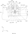
- the electrochemical apparatus 200 differs from the electrochemical apparatus 100 at least in that a third recess R is inward provided at a third end edge 2104 (that is, an edge of the first region 2100 opposite the seventh side 2103) of the first region 2100 in a second direction D 2 .
- the third recess R includes a first lateral side R 1 , a second lateral side R 2 , and a bottom side R 3 . In a third direction D 3 , the first lateral side R 1 and the second lateral side R 2 face each other.
- W 1 is approximately equal to W 2 .
- the third recess R may be inclined toward a side of the first region 2100.
- the first extension region 2112 and the second extension region 2113 are further defined to have a same size of L 2 in the second direction D 2 , and (L 2 + L 3 )/L 1 is set to be ⁇ 30%. (L 2 + L 3 )/L 1 is limited, so that in the second direction D 2 , a size of the first conductive material region 2111 covered by the first layer 50 is reduced, that is, an active material covered by the first layer 50 and unlikely to contribute to capacity is reduced, thereby reducing the impact of the first layer 50 on the capacity of the electrochemical apparatus 200.
- the first extension region 2112 and the second extension region 2113 have different sizes in the second direction D 2 .
- the size of the first extension region 2112 in the second direction D 2 is L 2
- the size of the second extension region 2113 in the second direction D 2 is L 2 '.
- (0.5L 2 + 0.5L 2 ' + L 3 )/L 1 may be defined to be ⁇ 30%.
- a distance between the first extension region 2112 and the first conductive plate 30 is W 3
- a distance between the second extension region 2113 and the first conductive plate 30 is W 4
- W 1 > W 3 , and W 2 > W 4 may also reduce a size proportion of the third recess R in the third direction D 3 and alleviate reduction of the heat dissipation area of the first region 2100 caused by provision of the third recess R.
- W 1 is approximately equal to W 2
- W 3 is approximately equal to W 4 .
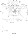
- the first extension region 2112 in the third direction D 3 , includes a ninth side 2114, and the second extension region 2113 includes a tenth side 2115.
- the ninth side 2114 is an inner edge of the first extension region 2112, and two ends of the ninth side 2114 are connected to the first lateral side R 1 and the fifth side 2101.
- the tenth side 2115 is an inner edge of the second extension region 2113, and two ends of the tenth side 2115 are connected to the second lateral side R 2 and the sixth side 2102.
- the first region 2100 is connected to the ninth side 2114 and the tenth side 2115.
- the ninth side 2114 and the tenth side 2115 are in a straight line shape.
- the ninth side 2114 and the tenth side 2115 may alternatively be in a convex arc shape away from the first region 2100.
- an end of the ninth side 2114 is connected to the first lateral side R 1 , and as compared with the embodiment shown in FIG. 10 , the other end portion of the ninth side 2114 connected to the fifth side 2101 may move downward along a direction opposite to the second direction D 2 .
- a region of the ninth side 2114 between the two end portions protrudes outward away from the first region 2100, so that the ninth side 2114 is in an arc shape.
- an end of the tenth side 2115 is connected to the second lateral side R 2 , and as compared with the embodiment shown in FIG. 10 , the other end portion of the tenth side 2115 connected to the sixth side 2102 may move downward along a direction opposite to the second direction D 2 .
- a region of the tenth side 2115 between the two end portions protrudes outward away from the first region 2100, so that the tenth side 2115 is in an arc shape.
- the first extension region 2112 and the second extension region 2113 both have a size of L 2
- a distance between the ninth side 2114 and the fourth side 3104 is L 4 , where L 2 ⁇ L 4 .
- L 4 represents a distance between the end portion of the ninth side 2114 connected to the first lateral side R 1 and the fourth side 3104.
- L 4 may reflect a length of a portion of the first region 2100 exposed from a side of the fourth side 3104 of the first conductive plate 30.
- L 2 is defined to be ⁇ L 4 , so that the relatively large L 4 helps to further increase the heat dissipation area of the first conductive plate 30, thereby reducing a temperature rise during large-current charging.
- a still another embodiment of this application further provides an electrochemical apparatus 300.
- the electrochemical apparatus 300 differs from the electrochemical apparatus 200 in that in the third direction D 3 , the first conductive plate 30 deviates from the central position of the first region 2100.
- W 3 ⁇ W 4 In some embodiments, W 3 ⁇ W 1 . In some embodiments, W 2 ⁇ W 4 .
- the electrochemical apparatus 100 (or the electrochemical apparatus 200 or 300) of this application includes all apparatuses in which an electrochemical reaction may take place.
- the electrochemical apparatus 100 includes all kinds of primary batteries, secondary batteries, fuel batteries, solar batteries, or capacitors (for example, super capacitors).
- the electrochemical apparatus 100 may be a lithium secondary battery, including a lithium metal secondary battery, a lithium-ion secondary battery, a lithium polymer secondary battery, and a lithium-ion polymer secondary battery.
- an embodiment of this application further provides an electronic apparatus 1.
- the electronic apparatus 1 includes the electrochemical apparatus 100 (or the electrochemical apparatus 200 or 300).
- the electrochemical apparatus 100 of this application is applicable to the electronic apparatuses 1 in various fields.
- the electronic apparatus 1 of this application may be but is not limited to a notebook computer, a pen-input computer, a mobile computer, an electronic book player, a portable telephone, a portable fax machine, a portable copier, a portable printer, a stereo headset, a video recorder, a liquid crystal television, a portable cleaner, a portable CD player, a mini-disc, a transceiver, an electronic notebook, a calculator, a memory card, a portable recorder, a radio, a standby power source, a motor, an automobile, a motorcycle, a motor bicycle, a bicycle, a lighting appliance, a toy, a game console, a clock, an electric tool, a flash lamp, a camera, a large household battery, and a lithium-ion capacitor.
- the charging process included: (1) the battery was constant-current charged to 4.25 V at 2.0C and constant-voltage discharged to 1.5C; (2) the battery was left standing for 5 min; (3) the battery was constant-current charged to 4.38 V at 1.5C and constant-voltage discharged to 1.0C; (4) the battery was left standing for 5 min; (5) the battery was constant-current charged to 4.43 V at 1.0C and constant-voltage discharged to 0.05C; and (6) the battery was left standing for 5 min. A temperature rise ⁇ t at a position close to the first conductive plate before and after charging was measured, and the result was recorded in Table 2.
Landscapes
- Chemical & Material Sciences (AREA)
- Chemical Kinetics & Catalysis (AREA)
- Electrochemistry (AREA)
- General Chemical & Material Sciences (AREA)
- Engineering & Computer Science (AREA)
- Manufacturing & Machinery (AREA)
- Materials Engineering (AREA)
- Secondary Cells (AREA)
- Connection Of Batteries Or Terminals (AREA)
- Electric Double-Layer Capacitors Or The Like (AREA)
- Sealing Battery Cases Or Jackets (AREA)
Abstract
Description
- This application relates to the field of energy storage technologies, and in particular, to an electrochemical apparatus and an electronic apparatus including such electrochemical apparatus.
- Electrochemical apparatuses (for example, batteries) are widely used in electronic products such as electronic mobile devices, electric tools, and electric vehicles, and increasingly high requirements are imposed on safety performance of the electrochemical apparatuses.
- During high-rate charging, an electrochemical apparatus is likely to continuously produce heat and have a temperature rise due to factors such as its internal resistance and polarization accumulation caused by charging. This may accelerate aging of the electrochemical apparatus as well as deterioration of capacity and power performance, and may also cause volumetric expansion, deformation, or the like, affecting the service life of a product.
- In view of the deficiencies of the prior art, it is necessary to propose an electrochemical apparatus that can solve the problem of temperature rise during charging.
- It is also necessary to provide an electronic apparatus including such electrochemical apparatus.
- This application provides an electrochemical apparatus including an electrode assembly and a first conductive plate. The electrode assembly is of a wound structure and includes a first electrode plate. The first electrode plate includes a first conductive layer and a first conductive material layer. The first conductive layer includes a first surface and a second surface opposite to each other. The first conductive material layer is provided on the first surface. The first surface includes a first region, the first conductive material layer includes a first recess, and the first region is exposed from the first recess. The first conductive plate is connected to the first region and extends out of the first electrode plate. The first conductive plate includes a third region and a fourth region connected to each other. A direction perpendicular to the third region is a first direction, and in the first direction, a projection of the third region is located in a projection of the first region, and a projection of the fourth region is located outside the projection of the first region. The third region includes a connection region, and the first conductive plate is connected to the first region through the connection region. Viewed from the first direction, the third region includes a first side, a second side, a third side, and a fourth side, the first side and the second side being opposite to each other, the third side and the fourth side being opposite to each other, and the fourth side being connected to the fourth region. The first region includes a fifth side, a sixth side, and a seventh side. An extension direction of the third region is a second direction, and in the second direction, the seventh side and the third side are arranged in sequence. In a third direction, the fifth side, the first side, the second side, and the sixth side are arranged in sequence. The first direction, the second direction, and the third direction are perpendicular to each other. a size of the third region in the third direction is T1, a size of the third region in the second direction is T2, an area of the projection of the third region in the first direction is S1, an area of a projection of the connection region in the first direction is S2, a distance between the first side and the fifth side is J1, a distance between the second side and the sixth side is J2, and a distance between the third side and the seventh side is J3, where S2/S1 + (J1 + J2 + J3)/(T1 + T2) ≥ 30%.
- In this application, S2/S1 may reflect a proportion of a current pass area of the first conductive plate. When S2/S1 is large, the current pass area of the first conductive plate increases, and current is distributed more dispersedly and uniformly on the first conductive plate during charging of the electrochemical apparatus, allowing for more dispersive heat production at the first conductive plate during large-current charging, thereby reducing the risk of local overheating of the first conductive plate. Moreover, (J1 + J2 + J3)/(T1 + T2) may reflect a proportion of a heat dissipation area in the first region. When (J1 + J2 + J3)/(T1 + T2) is large, the heat dissipation area of the first conductive plate increases, reducing a temperature rise during large-current charging. Therefore, in this application, a sum of S2/S1 and (J1 + J2 + J3)/(T1 + T2) is defined to be ≥ 30%, improving the safety and reliability of the electrochemical apparatus.
- In some possible implementations, the first electrode plate further includes a second conductive material layer provided on the second surface. The second surface includes a second region, the second conductive material layer includes a second recess, and the second region is exposed from the second recess. In the first direction, the projection of the first region and a projection of the second region at least partially overlap. Thus, heat produced at the first conductive plate may not only be dissipated through the first region exposed from the first conductive plate but also be transferred to the second region through overlapping portions of the first region and second region and dissipated through the second region, thereby further improving the heat dissipation efficiency.
- In some possible implementations, the electrochemical apparatus further includes a first layer adhered to the third region, where the first layer contains an insulating material. In the first direction, the projection of the third region is located in a projection of the first layer. The first layer may reduce the risk of generation of a short circuit caused when a burr or welding mark of the connection region punctures a separator, and may also be configured to compensate for a reduced thickness of a position where the first recess is provided on the first conductive material layer, allowing the electrochemical apparatus to have a more uniform overall thickness.
- In some possible implementations, the first conductive material layer includes a first conductive material region, where the first conductive material region encloses the first recess. The first layer is further adhered to the first conductive material region. In the first direction, the projection of the first region is located in the projection of the first layer.
- In some possible implementations, the electrochemical apparatus further includes a second layer, where the second layer contains an insulating material. The second conductive material layer includes a second conductive material region, where the second conductive material region encloses the second recess. The second layer is adhered to the second conductive material region. In the first direction, the projection of the second region is located in a projection of the second layer. The second layer may be configured to compensate for a reduced thickness of a position where the second recess is provided on the second conductive material layer.
- In some possible implementation, viewed from the first direction, the first layer includes an eighth side. In the second direction, the seventh side is disposed between the eighth side and the third side. A distance between an edge of the first region in the second direction and the eighth side is L1, and a distance between the seventh side and the eighth side is L3, where L3/L1 ≤ 30%. Thus, in the second direction, a size of the first conductive material region covered by the first layer is reduced, that is, an active material covered by the first layer and unlikely to contribute to capacity is reduced, thereby reducing the impact of the first layer on the capacity of the electrochemical apparatus.
- In some possible implementations, a third recess is provided at an edge of the first region in the second direction. The first conductive material region includes a first extension region and a second extension region extending toward the third recess. Viewed in the first direction, the first extension region and the second extension region are disposed on two sides of the third recess. Thus, when an electrode plate is slitted, a uniform thickness at an incision of the electrode plate helps to reduce the risk of formation of a wavy edge at the incision of the electrode plate.
- In some possible implementations, a distance between an edge of the first region in the second direction and the eighth side is L1, the first extension region and the second extension region have a same size of L2 in the second direction, and a distance between the seventh side and the eighth side is L3, where (L2 + L3)/L1 ≤ 30%. Thus, in the second direction, a size of the first conductive material region covered by the first layer is reduced, that is, an active material covered by the first layer and incapable of contributing to capacity is reduced, thereby reducing the impact of the first layer on the capacity of the electrochemical apparatus.
- In some possible implementations, a size of the first extension region in the third direction is W1, and a size of the second extension region in the third direction is W2, where (W1 + W2)/T1 ≥ 20%. Thus, reduction of the heat dissipation area of the first region caused by provision of the third recess is alleviated.
- In some possible implementations, a size of the first extension region in the third direction is W1, a size of the second extension region in the third direction is W2, a distance between the first extension region and the first conductive plate in the third direction is W3, and a distance between the second extension region and the first conductive plate in the third direction is W4. In some possible implementations, W3 < W1. In some possible implementations, W2 < W4. In some possible implementations, W3 < W4.
- In some possible implementations, in the third direction, the first extension region and the second extension region respectively include a ninth side and a tenth side. The first region is connected to the ninth side and the tenth side. The ninth side and the tenth side are in a straight line shape or an arc shape.
- In some possible implementations, in the second direction, the first extension region and/or the second extension region has a size of L2, and a distance between the ninth side and the fourth side is L4, where L2 < L4. The relatively large L4 helps to further increase the heat dissipation area of the first conductive plate, thereby reducing a temperature rise during large-current charging.
- In some possible implementations, L1 ranges from 10 mm to 50 mm. When L1 is large, the first conductive material layer covered by the first layer in the second direction has a relatively large size, and therefore has a greater impact on the capacity of the electrochemical apparatus. When L1 is small, the first region also has a small size in the second direction, so that the distance J3 between the third side and the seventh side is also small, and thus heat dissipation capability of the first region is also reduced.
- In some possible implementations, the electrochemical apparatus further includes a third layer and a fourth layer, where the third layer and the fourth layer each contain an insulating material. In the first direction, the first layer is disposed between the first conductive plate and the third layer, and the second layer is disposed between the first conductive plate and the fourth layer. The third layer and the fourth layer may further compensate for the reduced thickness of the electrode plate at the first recess and the second recess. When the first electrode plate is a negative electrode plate and the second electrode plate is a positive electrode plate, the third layer may also be configured to hinder movement, toward the second recess, of lithium ions deintercalated from a part of the third conductive material layer corresponding to the third layer in the first direction, thereby reducing the risks of excessive accumulation of lithium ions and formation of lithium dendrites due to the lack of lithium ions that may be embedded in the second recess. Similarly, the fourth layer may also reduce the risk of formation of lithium dendrites.
- In some implementations, the electrode assembly further includes a second electrode plate, and at least one of the third layer or the fourth layer is adhered to the second electrode plate. Thus, the third layer and the fourth layer are fixed in the electrochemical apparatus and serves to compensate for thickness or reduce the risk of formation of lithium dendrites.
- In some possible implementations, in the second direction, an edge of at least one of the first layer or the second layer extends beyond an edge of the first electrode plate.
- In some possible implementations, the connection region is welded to the first region, thereby providing a higher connection strength between the first conductive plate and the first region. The connection region includes a plurality of welding spots. The area S2 is a sum of projection areas of a plurality of welding spots in the first direction.
- In some possible implementations, the electrode assembly further includes a second electrode plate and a separator. The first electrode plate, the separator, and the second electrode plate are stacked and wound to form the electrode assembly. In the winding direction, the electrode assembly includes a first section, a first bent section, a second section, and a second bent section connected in sequence. The first conductive plate is located in the first section, thereby improving the flatness of the first conductive plate when the first conductive plate is connected to the first region.
- In some possible implementations, the housing includes a body for accommodating the electrode assembly and an sealing edge connected to the body. The sealing edge includes a polymer layer, and the fourth region extends out of the housing from the polymer layer.
- This application further provides an electronic apparatus including the foregoing electrochemical apparatus.
-
-
FIG. 1 is a schematic diagram of an overall structure of an electrochemical apparatus according to an embodiment of this application. -
FIG. 2 is a schematic structural diagram of the electrochemical apparatus shown inFIG. 1 before packaging. -
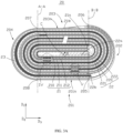
FIG. 3A is a top view of an electrode assembly of the electrochemical apparatus shown inFIG. 1 . -
FIG. 3B is a schematic diagram of preparation of an sealing edge of a housing of the electrochemical apparatus shown inFIG. 1 . -
FIG. 4 is an enlarged view of the electrode assembly at position IV shown inFIG. 3A . -
FIG. 5 is an enlarged view of the electrode assembly at position V shown inFIG. 3A . -
FIG. 6 is a schematic structural diagram of front and rear surfaces of an unfolded first electrode plate of the electrode assembly shown inFIG. 3A . -
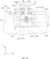
FIG. 7 is a front view of a joint between a first conductive plate and the first electrode plate shown inFIG. 3A . -
FIG. 8A is a front view after a first bonding member on the first electrode plate shown inFIG. 7 is removed. -
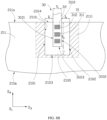
FIG. 8B is a front view after a first bonding member on the first electrode plate shown inFIG. 7 is removed according to some other embodiments. -
FIG. 8C is a schematic view of a projection of a third region of a first conductive plate shown inFIG. 8B . -
FIG. 8D is a schematic view of a projection of a connection region of the third region shown inFIG. 8B . -
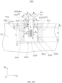
FIG. 9 is a front view of a joint between a first electrode plate and a first conductive plate of an electrochemical apparatus according to another embodiment of this application. -
FIG. 10A is a front view after a first bonding member on the first electrode plate shown inFIG. 9 is removed. -
FIG. 10B is a front view after a first bonding member on the first electrode plate shown inFIG. 9 is removed according to some other embodiments. -
FIG. 10C is a front view after a first bonding member on the first electrode plate shown inFIG. 9 is removed according to some other embodiments. -
FIG. 10D is a front view after a first bonding member on the first electrode plate shown inFIG. 9 is removed according to some other embodiments. -
FIG. 10E is a front view after a first bonding member on the first electrode plate shown inFIG. 9 is removed according to some other embodiments. -
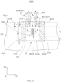
FIG. 11 is a front view of a joint between a first electrode plate and a first conductive plate according to some other embodiments. -
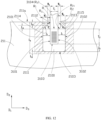
FIG. 12 is a front view after a first bonding member on the first electrode plate shown inFIG. 11 is removed. -
FIG. 13 is a front view of a joint between a first electrode plate and a first conductive plate of an electrochemical apparatus according to another embodiment of this application. -
FIG. 14 is a schematic diagram of an overall structure of an electronic apparatus according to an embodiment of this application. - The following clearly describes in detail the technical solutions in some embodiments of this application. Apparently, the described embodiments are merely some rather than all of the embodiments of this application. Unless otherwise defined, all technical and scientific terms used herein shall have the same meanings as commonly understood by persons skilled in the art to which this application belongs. The terms used in the specification of this application are merely intended to describe specific embodiments rather than to constitute any limitation on this application.
- The following describes some embodiments of this application in detail. However, this application may be embodied in many different implementations and should not be construed as being limited to the example embodiments set forth herein. Rather, these example embodiments are provided so that this application may be conveyed to persons skilled in the art thoroughly and in detail.
- In addition, in the accompanying drawings, sizes or thicknesses of various components and layers may be exaggerated for brevity and clarity. Throughout the text, the same numerical values represent the same elements. As used herein, the term "and/or" includes any and all combinations of one or more of the associated listed items. In addition, it should be understood that when an element A is referred to as being "connected to" an element B, the element A may be directly connected to the element B or an intervening element C may be present therebetween such that the element A and the element B may be indirectly connected to each other.
- Further, the use of "may" for describing some embodiments of this application relates to "one or more embodiments of this application."
- The terminology used herein is merely intended to describe specific embodiments rather than to constitute any limitation on this application. As used herein, the singular forms are intended to include the plural forms as well, unless the context clearly indicates otherwise. It should be further understood that the term "comprise" or "include", when used in this specification, specifies the presence of stated features, numbers, steps, operations, elements, and/or components but do not preclude the presence or addition of one or more other features, numbers, steps, operations, elements, components, and/or combinations thereof.
- Spatial related terms such as "above" may be used herein for ease of description to describe the relationship between one element or feature and another element (a plurality of elements) or feature (a plurality of features) as illustrated in the figure. It should be understood that spatial related terms are intended to encompass different orientations of a device or an apparatus in use or operation in addition to the orientations depicted in the figures. For example, if the device in the figures is turned over, elements described as "above" or "over" other elements or features would then be oriented "below" or "beneath" the other elements or features. Thus, the example term "above" may encompass both an orientation of above and below. It should be understood that although the terms first, second, third, or the like may be used herein to describe various elements, components, regions, layers, and/or portions, these elements, components, regions, layers, and/or portions should not be limited by these terms. These terms are used to distinguish one element, component, region, layer, or portion from another element, component, region, layer, or portion. Therefore, the first element, component, region, layer, or portion discussed below may be referred to as the second element, component, region, layer, or portion without departing from the teachings of the example embodiments.
- Referring to
FIG. 1 andFIG. 2 , an embodiment of this application provides anelectrochemical apparatus 100 including ahousing 10, anelectrode assembly 20, a firstconductive plate 30, and a secondconductive plate 40. Theelectrode assembly 20 is located inside thehousing 10 and is of a wound structure. The firstconductive plate 30 and the secondconductive plate 40 are both electrically connected to theelectrode assembly 20 and extend out of thehousing 10 from the inside of thehousing 10. As shown inFIG. 2 , there is oneelectrode assembly 20. In other embodiments, there may be a plurality ofelectrode assemblies 20. The plurality ofelectrode assemblies 20 are located inside thehousing 10 and are electrically connected in parallel or in series. Referring toFIG. 3A , theelectrode assembly 20 includes afirst electrode plate 21, asecond electrode plate 22, and aseparator 23, where theseparator 23 is disposed between thefirst electrode plate 21 and thesecond electrode plate 22. Thefirst electrode plate 21, theseparator 23, and thesecond electrode plate 22 are sequentially stacked and wound to form theelectrode assembly 20. As shown inFIG. 3A , theelectrode assembly 20 has a winding center axis C perpendicular to a paper plane. A winding direction D is a direction of a counterclockwise rotation around the winding center axis C as shown inFIG. 3A . In some embodiments, the winding direction D may also be a direction of a counterclockwise rotation. - In this application, a first three-dimensional coordinate system is established based on the first direction D1, the second direction D2, and the third direction D3 perpendicular to each other. The first direction D1 is a direction perpendicular to the
third region 31 of the firstconductive plate 30. The second direction D2 is an extension direction of thethird region 31 of the firstconductive plate 30. When the electrode plate is unfolded, a second three-dimensional coordinate system is established based on the first direction D1, the second direction D2, and a fourth direction D4 perpendicular to each other. The fourth direction D4 is a direction from a winding start end to a winding stop end of the electrode plate before winding. For example, the fourth direction D4 is a direction from a first windingstart end 21a to a first windingstop end 21b of thefirst electrode plate 21, and also a direction from a second windingstart end 22a to a second windingstop end 22b of thesecond electrode plate 22. - In some embodiments, in the winding direction D, the
electrode assembly 20 includes afirst section 201, a firstbent section 202, asecond section 203, and a secondbent section 204 that are connected in sequence. The first direction D1 is a direction in which thefirst electrode plate 21 in thefirst section 201 orsecond section 203 is stacked. Theelectrode assembly 20 may include a plurality offirst sections 201, a plurality of firstbent sections 202, a plurality ofsecond sections 203, and a plurality of secondbent sections 204. In some embodiments, thefirst section 201 and thesecond section 203 may be flat and straight sections. In some other embodiments, in the winding direction D, theelectrode assembly 20 may alternatively include four bent sections that are connected in sequence. - The
first section 201 has a first outer surface 201a, and thesecond section 203 has a second outer surface 203a. A joint between the outermostfirst section 201 of theelectrode assembly 20 and the outermost firstbent section 202 of theelectrode assembly 20 is afirst end 205. Thefirst end 205 is a start portion of a rightmost bent side of the firstbent section 202 inFIG. 3A in the winding direction D, and thefirst end 205 is also a portion where a dotted line B-B formed by extension, of an innermost bent side at the right in theelectrode assembly 10, in the first direction D1 is intersected with the first outer surface 201a. A joint between the outermost firstbent section 202 of theelectrode assembly 20 and the outermostsecond section 203 of theelectrode assembly 20 is asecond end 206. Thesecond end 206 is a stop portion of the rightmost bent side of the firstbent section 202 inFIG. 3A in the winding direction D, and thesecond end 206 is also a portion where the dotted line B-B formed by extension, of the innermost bent side at the right in theelectrode assembly 10, in the first direction D1 is intersected with the second outer surface 203a. A joint between the outermostsecond section 203 of theelectrode assembly 20 and the outermost secondbent section 204 of theelectrode assembly 20 is athird end 207. Thethird end 207 is a start portion of a leftmost curve of the secondbent section 204 inFIG. 3A in the winding direction D, and thethird end 207 is also a portion where a dotted line A-A formed by extension, of the innermost bent side at the left in theelectrode assembly 10, in the first direction D1 is intersected with the second outer surface 203a. A joint between the outermost secondbent section 204 of theelectrode assembly 20 and the outermostfirst section 201 of theelectrode assembly 20 is afourth end 208. Thefourth end 208 is a stop portion of the leftmost curve of the secondbent section 204 inFIG. 3A in the winding direction D, and thefourth end 208 is also a portion where the dotted line A-A formed by extension, of the innermost bent side at the left in theelectrode assembly 10, in the first direction D1 is intersected with the first outer surface 201a. In the first direction D1, thefirst end 205 and thesecond end 206 are aligned, and thethird end 207 and thefourth end 208 are aligned. - Referring to
FIG. 3A ,FIG. 4 , andFIG. 5 , thefirst electrode plate 21 includes a firstconductive layer 210, a firstconductive material layer 211, and a secondconductive material layer 212. The firstconductive layer 210 includes afirst surface 210a and asecond surface 210b opposite to the each other in the first direction D1. Thefirst material layer 211 is disposed on thefirst surface 210a, and the secondconductive material layer 212 is disposed on thesecond surface 210b. Thesecond electrode plate 22 includes a secondconductive layer 220, a thirdconductive material layer 221, and a fourthconductive material layer 222. The secondconductive layer 220 includes athird surface 220a and afourth surface 220b opposite to each other in the first direction D1. Thethird material layer 221 is disposed on thethird surface 220a, and the fourthconductive material layer 222 is disposed on thefourth surface 220b. The secondconductive material layer 212 and the thirdconductive material layer 221 face each other with aseparator 23 located therebetween in the first direction D1. In some embodiments, as shown inFIG. 3A , after stacking and winding, thefirst surface 210a of the firstconductive layer 210 is far away from the winding center axis C, and thesecond surface 210b is toward the winding center axis C. Thethird surface 220a of the secondconductive layer 220 is far away from the winding center axis C, and thefourth surface 220b is toward the winding center axis C. It should be understood that in other embodiments, thefirst surface 210a of the firstconductive layer 210 may be toward the winding center axis C, and thesecond surface 210b is far away from the winding center axis C. In this case, thethird surface 220a of the secondconductive layer 220 is toward the winding center axis C, and thefourth surface 220b is far away from the winding center axis C. - The
first electrode plate 21 may be a positive electrode plate or a negative electrode plate. Correspondingly, the firstconductive layer 210 may be a positive electrode conductive layer or a negative electrode conductive layer, and the firstconductive material layer 211 and the secondconductive material layer 212 may each be a positive electrode active material layer or a negative electrode active material layer. The firstconductive layer 210 may have a current collection function. Thesecond electrode plate 22 may be a positive electrode plate or a negative electrode plate. Correspondingly, the secondconductive layer 220 may be a negative electrode conductive layer or a positive electrode conductive layer, and the thirdconductive material layer 221 and the fourthconductive material layer 222 may each be a negative electrode active material layer or a positive electrode active material layer. The secondconductive layer 220 may have a current collection function. In some embodiments, thefirst electrode plate 21 is a positive electrode plate, and thesecond electrode plate 22 is a negative electrode plate. The positive electrode conductive layer may be an aluminum foil or a nickel foil, and the negative electrode conductive layer may be at least one of a copper foil, a nickel foil, or a carbon-based conductive layer. - The positive electrode active material layer includes a positive electrode active material, and the positive electrode active material includes a compound that reversibly intercalates and deintercalates lithium ions (that is, a lithiated intercalation compound). In some embodiments, the positive electrode active material may include a lithium transition metal composite oxide. The lithium transition metal composite oxide contains lithium and at least one element selected from cobalt, manganese, and nickel. In some embodiments, the positive electrode active material is selected from at least one of lithium cobalt oxide (LiCoO2), a lithium nickel manganese cobalt ternary material (NCM), lithium manganese oxide (LiMn2O4), lithium nickel manganese oxide (LiNi0.5Mn1.5O4), or lithium iron phosphate (LiFePO4).
- The negative electrode active material layer contains a negative electrode active material. A negative electrode active material that is known in the art and that may reversibly intercalate and deintercalate active ions may be used. This is not limited in this application. For example, the negative electrode active material may be but is not limited to one or a combination of more of graphite, soft carbon, hard carbon, carbon fiber, meso-carbon microbeads, a silicon-based material, a tin-based material, lithium titanate, another metal that may form an alloy with lithium, or the like. The graphite may be selected from one or a combination of more of artificial graphite, natural graphite, or modified graphite. The silicon-based material may be selected from one or a combination of more of elemental silicon, a silicon-oxygen compound, a siliconcarbon composite, or a silicon alloy. The tin-based material may be selected from one or a combination of more of elemental tin, a tin-oxygen compound, a tin alloy, or the like.
- The
separator 23 includes at least one of polyethylene, polypropylene, polyvinylidene fluoride, polyethylene terephthalate, polyimide, or aramid. For example, polyethylene is selected from at least one of high-density polyethylene, low-density polyethylene, or ultrahigh-molecular-weight polyethylene. Polyethylene and polypropylene have a good effect on alleviating short circuits and may improve the stability of a battery through a shutdown effect. - Referring to
FIG. 4 andFIG. 6 toFIG. 8A , thefirst surface 210a of the firstconductive layer 210 includes afirst region 2100. The firstconductive material layer 211 includes afirst recess 2110. Thefirst recess 2110 may be formed by opening afirst end edge 211a of the firstconductive material layer 211 inward in a direction of the winding center axis C, and thefirst recess 2110 does not run through asecond end edge 211b of the firstconductive material layer 211 in the direction of the winding center axis C. Thefirst region 2100 is exposed from thefirst recess 2110, and thefirst region 2100 is separated from the firstconductive material layer 211. Specifically, thefirst recess 2110 may be formed by laser cleaning in the firstconductive material layer 211 so that thefirst region 2100 is exposed. Alternatively, thefirst region 2100 may be bonded with polystyrene foam, coated with an active material, and then heated to make the polystyrene foam fall off, so that thefirst region 2100 is exposed. Alternatively, the active material on thefirst region 2100 may be directly scraped using a scraper, so that thefirst region 2100 is exposed. However, it can be understood that after laser cleaning or scraping using a scraper, there is still a small amount of active material on the surface of thefirst region 2100. This is not limited in this application. Viewed in the first direction D1, the firstconductive plate 30 is connected to thefirst region 2100 and extends out of thefirst region 2100 and beyond thefirst end edge 211a from thefirst region 2100, allowing for a connection to an external component (not shown in the figure). In order to meet the requirements of large-current charging, thefirst region 2100 may be disposed in an area other than a winding head and a winding tail of thefirst electrode plate 21. In some embodiments, the projections of thefirst region 2100 and thefirst recess 2110 in the first direction D1 may both be rectangular. In some specific embodiments, the projections of thefirst region 2100 and thefirst recess 2110 in the first direction D1 are both rectangular. - In some embodiments, the
housing 10 may be a package bag obtained using a package film (for example, an aluminum-plastic film) for packaging, which means that theelectrochemical apparatus 100 may be a soft pack battery. Referring toFIG. 1 andFIG. 2 , thehousing 10 includes abody 11 for accommodating theelectrode assembly 20 and an sealingedge 12 connected to thebody 11. Thebody 11 includes afirst wall 111 and asecond wall 112 opposite to each other in the second direction D2. The sealingedge 12 is connected to thefirst wall 111 and further includes athird wall 113 and afourth wall 114 opposite to each other in the second direction D2. In the second direction D2, thethird wall 113 is disposed between thefirst wall 111 and thesecond wall 112, and thefourth wall 114 is also disposed between thefirst wall 111 and thesecond wall 112. The firstconductive plate 30 and the secondconductive plate 40 respectively extend out of the sealingedge 12 from the inside of thehousing 10 to the outside of thehousing 10. Thehousing 10 includes afirst housing 13 and asecond housing 14 opposite to each other. Thehousing 10 may be formed by heat-sealing thefirst housing 13 and thesecond housing 14. Thefirst housing 13 is provided with afirst space 130, and thesecond housing 14 is a flat plate structure. Thus, after thefirst housing 13 and thesecond housing 14 are heat-sealed, thefirst space 130 is enclosed by thesecond housing 14 to form an accommodating space for accommodating theelectrode assembly 20. Certainly, thefirst housing 14 may also have a second space (not shown in the figure). After thefirst housing 13 and thesecond housing 14 are heat-sealed, thefirst space 130 and the second space cooperate with each other to form an accommodating space for accommodating theelectrode assembly 20. - Referring to
FIG. 3B , thefirst housing 13 and thesecond housing 14 may be obtained by folding a package film. That is, thefirst housing 13 and thesecond housing 14 are both multi-layer sheets. The multi-layer sheet includes aprotective layer 131, ametal layer 132, and apackage layer 133 stacked in sequence. Theprotective layer 131 may be made of a polymer material, which may be used to protect themetal layer 132, reduce the risk of damage to themetal layer 132 due to external forces, and also slow down permeation of air from an external environment, thereby maintaining a normal operating environment inside theelectrochemical apparatus 100. The polymer material of theprotective layer 131 may be selected from at least one of polyethylene terephthalate, polybutylene terephthalate, polyvinylidene fluoride, polytetrafluoroethylene, polypropylene, polyamide, or polyimide. Themetal layer 132 may be used to delay penetration of moisture from the external environment and reduce damage to theelectrode assembly 20 caused by external forces. In some embodiments, themetal layer 132 may be an aluminum foil layer or a steel foil layer. Thepackage layer 133 may be used for packaging and may reduce the risk of dissolution or swelling of the multi-layer sheet by an organic solvent in an electrolyte. Thepackage layer 133 may also be used for reducing the risk of corrosion of the metal layer caused by contact between an electrolytic salt in the electrolyte and themetal layer 132. Thepackage layer 133 includes a polymer material with a property of being melted when heated. The polymer material may be selected from at least one of polypropylene, a propylene copolymer, polyethylene, or polymethyl methacrylate. During preparation of thehousing 10, a certain temperature and pressure may be applied to edges of thefirst housing 13 and thesecond housing 14 using a package head, such that thepackage layer 133 of thefirst housing 13 and thepackage layer 133 of thesecond housing 14 are melted and bonded together to obtain apolymer layer 134. Therefore, after the sealingedge 12 is formed through heat sealing, the sealingedge 12 may include aprotective layer 131, ametal layer 132, apolymer layer 134, ametal layer 132, and aprotective layer 131 stacked in sequence. - In some other embodiments, the
electrochemical apparatus 100 is not limited to a soft pack battery and may alternatively be a steel-shell battery, an aluminum-shell battery, or the like, which is not limited in this application. - An
electrochemical apparatus 200 includes anelectrode assembly 20 and a firstconductive plate 30; theelectrode assembly 20 includes afirst electrode plate 21; thefirst electrode plate 21 includes a firstconductive layer 210 and a firstconductive material layer 212; where - the first
conductive layer 210 includes afirst surface 210a and asecond surface 210b toward an opposite direction with respect to thefirst surface 210a; and viewed along a first direction D1 perpendicular to thefirst surface 210a, the firstconductive layer 210 further includes afirst end edge 211b in a second direction D2 perpendicular to the first direction D1, and asecond end edge 211a that is located on a side opposite to thefirst end edge 211b in the second direction D2 and that has a third recess R viewed along the second direction D2; - the first
conductive material layer 211 is disposed on thefirst surface 210a of the firstconductive layer 210, separated from at least a part of a fourth recess 4, and arranged from thesecond end edge 211a to thefirst end edge 211b; and - the first
conductive plate 30 is disposed on thefirst surface 210a of the firstconductive layer 210, is separated from the firstconductive material layer 210, and overlaps with a third recess R viewed along the first direction D1. - In the electrochemical apparatus described above, viewed along the first direction D1, the first
conductive material layer 210 includes a portion connected to thesecond end edge 210a and the third recess R. - In the electrochemical apparatus described above, viewed along the first direction D1, in a third direction D3 perpendicular to a second direction D2, the first
conductive material layer 210 includes a first lateral side R1 connected to thesecond end edge 211a and opposite the firstconductive plate 30. - In the electrochemical apparatus described above, viewed along the first direction D1, in the third direction D3, the first
conductive material layer 210 includes afifth side 2101 separated from the first lateral side R1 and opposite the firstconductive plate 30. - In the electrochemical apparatus described above, the first
conductive material layer 210 includes aninth side 2114 connected to the first lateral side R1 and thefifth side 2101. - In the electrochemical apparatus described above, a distance W3 from the first
conductive plate 30 to the first lateral side R1 in the third direction D3 is shorter than a distance W1 from the first lateral side R1 to thefifth side 2101 in the third direction D3. - In the electrochemical apparatus described above, viewed along the first direction D1, the first
conductive material layer 210 includes a portion connected to thesecond end edge 210a and the third recess R; and viewed along the first direction D1, in the third direction D3 perpendicular to the second direction D2, the firstconductive material layer 210 further includes a second lateral side R2 connected to thesecond end edge 211a and opposite the firstconductive plate 30, and asixth side 2102 separated from the second lateral side R2 and opposite the firstconductive plate 30. - In the electrochemical apparatus described above, the first
conductive material layer 210 includes atenth side 2115 connected to the second lateral side R2 and thesixth side 2102. - In the electrochemical apparatus described above, a distance W4 from the first
conductive plate 30 to the second lateral side R2 is shorter than a distance W2 from the second lateral side R2 to thetenth side 2115 in the third direction D3. - In the electrochemical apparatus described above, in the third direction D3, the distance W3 from the first
conductive plate 30 to the first lateral side R1 is shorter than a distance W4 from the firstconductive plate 30 to the second lateral side R2. - In the electrochemical apparatus described above, a distance L2 from the
second end edge 211a to theninth side 2114 in the second direction D2 is shorter than a distance L4 from theninth side 2114 to a bottom edge R3 of the third recess R in the second direction D2. - In the electrochemical apparatus described above, the third recess R includes a slope edge R11 extending from the
second end edge 211a to the bottom edge R3 of the third recess. - In the electrochemical apparatus described above, the
electrode assembly 20 includes afirst layer 50 that at least covers a part of thefirst electrode plate 30 and the first lateral side R1 and that includes an insulating material. - As shown in
FIG. 7 andFIG. 8A , the firstconductive plate 30 includes athird region 31 and afourth region 32 connected to thethird region 31. In the first direction D1, a projection of thethird region 31 is located in a projection of thefirst region 2100, that is, the projection of thethird region 31 overlaps with at least a part of the projection of thefirst region 2100, while a projection of thefourth region 32 is located outside the projection of thefirst region 2100. With reference toFIG. 1 , thefourth region 32 extends out of thehousing 10. With reference toFIG. 1 andFIG. 3B , when theelectrochemical apparatus 100 is a soft pack battery, thefourth region 32 extends out of thehousing 10 from thepolymer layer 134 in the sealingedge 12. In some embodiments, a surface where the sealingedge 12 is located is perpendicular to a surface where thefirst wall 111 is located. In this case, the second direction D2 not only is an extension direction of thethird region 31 but also may be an extension direction of afirst tab 30. However, in other embodiments, the sealingedge 12 may also be folded to thefirst wall 111 to reduce a size of theelectrochemical apparatus 100 in the second direction D2, thereby increasing utilization rate and energy density. In this case, the second direction D2 is an extension direction of thethird region 31, while an extension direction of thefourth region 32 in the sealingedge 12 is perpendicular of the second direction D2. - The
third region 31 includes aconnection region 311 and anedge region 312 provided around theconnection region 311. The firstconductive plate 30 is connected to thefirst region 2100 through theconnection region 311, that is, theconnection region 311 is a position through which current flows during charging of theelectrochemical apparatus 100. In some embodiments, the firstconductive plate 30 is welded to thefirst region 2100 through theconnection region 311, thereby providing a high connection strength between the firstconductive plate 30 and thefirst region 2100. A plurality ofwelding spots 3110 may be formed after theconnection region 311 and thefirst region 2100 are welded, and theconnection region 311 and thefirst region 2100 are fixed through the welding spots 3110. When there are a large number ofwelding spots 3110, contact resistance between the firstconductive plate 30 and thefirst electrode plate 21 may be reduced, thereby reducing heat production during charging of theelectrochemical apparatus 100. In other embodiments, the firstconductive plate 30 may alternatively be connected to thefirst region 2100 through a conductive adhesive or in other manners. - In some embodiments, as shown in
FIG. 7 andFIG. 8A , viewed from the first direction D1, the plurality ofwelding spots 3110 may be arranged in a single matrix. In this case, theedge region 312 is a region outside an outermost circle ofwelding pads 3110 in thethird region 31. In some other embodiments, as shown inFIG. 8B , the plurality ofwelding spots 3110 may alternatively be arranged in a plurality of matrices, such that theconnection region 311 includes a plurality of separated regions. In this case, theedge region 312 further includes a region located between adjacent two of the matrices in thethird region 31. - As shown in
FIG. 7 andFIG. 8A , viewed from the first direction D1, thethird region 31 is approximately rectangular. Thethird region 31 includes afirst side 3101, asecond side 3102, athird side 3103, and afourth side 3104. Thefirst side 3101 andsecond side 3102 face each other in the third direction D3. Thethird side 3103 andfourth side 3104 face each other in the second direction D2. Thethird side 3103 connects two connecting end portions of thefirst side 3101 and thesecond side 3102, and thefourth side 3104 connects the two connecting end portions of thefirst side 3101 and thesecond side 3102. In addition, thefourth side 3104 is boundary of thethird region 31 and thefourth region 32, the fourth region and the fourth region. In some embodiments, thefirst side 3101 and thesecond side 3102 extend along the second direction D2, respectively; and thethird side 3103 and thefourth side 3104 extend along the third direction D3. - The
first region 2100 includes afifth side 2101, asixth side 2102, and aseventh side 2103. Thefifth side 2101 andsixth side 2102 face each other in the third direction D3. Theseventh side 2103 connects two connecting end portions of thefifth side 2101 and thesixth side 2102. Viewed in the first direction D1, theseventh side 2103 faces athird end edge 2104 of thefirst region 2100 in the second direction D2. It can be understood that thefirst recess 2110 is a three-dimensional structure. However, viewed from the first direction D1, thefirst recess 2100 includes a plurality of sequentially connected sides (not shown in the figure). In addition, viewed from the first direction D1, thefifth side 2101, thesixth side 2102, and theseventh side 2103 of thefirst region 2100 overlap with the sides of thefirst recess 2110, respectively. In some embodiments, thefifth side 2101 and thesixth side 2102 extend along the second direction D2, respectively; and theseventh side 2103 extends along the third direction D3. In the second direction D2, theseventh side 2103 and thethird side 3103 are arranged in sequence, and theseventh side 2103 and thethird side 3103 at least partially face each other. In some embodiments, theseventh side 2103 and thethird side 3103 may be parallel to each other. In the third direction D3, thefifth side 2101, thefirst side 3101, thesecond side 3102, and thesixth side 2102 are arranged in sequence; thefifth side 2101 and thefirst side 3101 at least partially face each other; and thesecond side 3102 and thesixth side 2102 at least partially face each other. In some embodiments, thefifth side 2101, thefirst side 3101, thesecond side 3102, and thesixth side 2102 may be parallel to each other. - In the second direction D2, the
seventh side 2103 and thethird side 3103 are arranged in sequence, meaning that a virtual straight line provided along the second direction D2 runs through theseventh side 2103 and thethird side 3103 in sequence. In the third direction D3, thefifth side 2101, thefirst side 3101, thesecond side 3102, and thesixth side 2102 are arranged in sequence, meaning that a virtual straight line provided along the third direction D3 runs through thefifth side 2101, thefirst side 3101, thesecond side 3102, and thesixth side 2102. In some embodiments, the second direction D2 is the direction of the winding center axis C, and the third direction D3 is perpendicular to the second direction D2. - In some embodiments, as shown in
FIG. 7 andFIG. 8A , thefifth side 2101, thesixth side 2102, and theseventh side 2103 are all in a straight line shape. In some other embodiments, when thefirst region 2100 is formed by laser cleaning or the like, at least one of thefifth side 2101, thesixth side 2102, or theseventh side 2103 may be in a concave-convex shape. This is not limited in this application. - As shown in
FIG. 7 andFIG. 8A , in the third direction D3, the firstconductive plate 30 is disposed at an approximately central position of thefirst region 2100. - A size of the
third region 31 in the third direction D3 is T1, a size of thethird region 31 in the second direction D2 is T2, an area of the projection of thethird region 31 in the first direction D1 is S1 (shown inFIG. 8C ), an area of the projection of theconnection region 311 in the first direction D1 is S2 (shown inFIG. 8D ), a distance between thefirst side 3101 and thefifth side 2101 is J1, a distance between thesecond side 3102 and thesixth side 2102 is J2, and a distance between thethird side 3103 and theseventh side 2103 is J3, where a heat dissipation coefficient K of thefirst region 2100 satisfies K = S2/S1 + (J1 + J2 + J3)/(T1 + T2) ≥ 30%. - S2/S1 may reflect an area proportion of the
connection region 311 in thethird region 31, that is, a proportion of a current pass area of the firstconductive plate 30. When S2/S1 is large, the current pass area of the firstconductive plate 30 increases, and current is distributed more dispersedly and uniformly on the firstconductive plate 30 during charging of theelectrochemical apparatus 100, allowing for more dispersive heat production at the firstconductive plate 30 during large-current charging, thereby reducing the risk of local overheating of the firstconductive plate 30. Moreover, J1 may reflect a length of a portion of thefirst region 2100 exposed from a side of thefirst side 3101 of the firstconductive plate 30; J2 may reflect a length of a portion of thefirst region 2100 exposed from a side of thesecond side 3102 of the firstconductive plate 30; and J3 may reflect a length of a portion of thefirst region 2100 exposed from a side of thethird side 3103 of the firstconductive plate 30. Therefore, (J1 + J2 + J3)/(T1 + T2) may reflect a proportion of an area of thefirst region 2100 exposed from the firstconductive plate 30, that is, a proportion of a heat dissipation area in thefirst region 2100. When (J1 + J2 + J3)/(T1 + T2) is large, the heat dissipation area of the firstconductive plate 30 increases, reducing a temperature rise during large-current charging. Therefore, in this application, the heat dissipation coefficient K of thefirst region 2100 is a sum of S2/S1 and (J1 + J2 + J3)/(T1 + T2), and the heat dissipation coefficient K is set to be ≥ 30%, improving the safety and reliability of theelectrochemical apparatus 100. - J1, J2, J3, T1, and T2 may be directly measured using a direct measurement method, respectively. Measurement steps include: disassembling the
electrochemical apparatus 100, and taking thefirst electrode plate 21 as a test sample; and directly measuring values of J1, J2, J3, T1, and T2 using a caliper or another appropriate measuring instrument, or acquiring an image of thefirst electrode plate 21, and performing measurement in the image. - S1 may be calculated according to T1 and T2 in combination with a specific shape of the
third region 31. It can be understood that when thethird region 31 is rectangular, S1 is a product of T1 and T2. - In some embodiments, when the
connection region 311 is welded to thefirst region 2100, S2 is a sum of projection areas of the plurality ofwelding spots 3110 in the first direction D1. As shown inFIG. 8D , if the number of thewelding spots 3110 is n (n is a natural number greater than 1), projection areas of then welding spots 3110 in the first direction D1 are respectively S21, S22, ..., and S2n, and S2 = S21 + S22 + ... + S2n. S2 may be measured using an image method. Measurement steps include: disassembling theelectrochemical apparatus 100, taking thefirst electrode plate 21 as a test sample, and acquiring an image including theconnection region 311 in the first direction D1, as a first image; acquiring an image of a reference target with a known area of S0, as a second image; calculating the number n1 of pixel points corresponding to thewelding spots 3110 in the first image, and calculating the number n0 of pixel points corresponding to the reference target in the second image; and calculating an area S2 of thewelding spots 3110 according to the area A0, the number n1, and the number n0, where S2 = (S0 × n0)/n1. It can be understood that measurement of S2 is not limited to the above method. In other embodiments, when theconnection region 311 is connected to thefirst region 2100 in another manner, S1 may alternatively be obtained through calculation according to a size of each dimension of theconnection region 311 and a specific shape of theconnection region 311. - Referring to
FIG. 4 , in some embodiments, thesecond surface 210b of the firstconductive layer 210 is defined to include asecond region 2105. The secondconductive material layer 212 includes asecond recess 2120. Thesecond region 2105 is exposed from thesecond recess 2120, and thesecond region 2105 is separated from the secondconductive material layer 212. However, it can be understood that a small amount of active material may be left on the surface of thesecond region 2105. This is not limited in this application. In the first direction D1, the projection of thefirst region 2100 and a projection of thesecond region 2105 at least partially overlap. Thus, heat produced at the firstconductive plate 30 may not only be dissipated through thefirst region 2100 exposed from the firstconductive plate 30 but also be transferred to thesecond region 2105 through overlapping portions of thefirst region 2100 andsecond region 2105 and dissipated through thesecond region 2105, thereby further improving the heat dissipation efficiency. In some specific embodiments, in order to further improve the heat dissipation efficiency, in the first direction D1, the projection of thefirst region 2100 and the projection of thesecond region 2105 may be set to totally overlap. - It can be understood that when the first
conductive plate 30 is welded to thefirst region 2100 through theconnection region 311, a burr or welding mark may be formed at theconnection region 311, and the burr or welding mark may puncture theseparator 23, causing a short circuit. As shown inFIG. 4 ,FIG. 6 , andFIG. 7 , In some embodiments, theelectrochemical apparatus 100 further includes afirst layer 50 at least adhered to thethird region 31, where thefirst layer 50 contains an insulating material. In the first direction D1, the projection of thefirst region 2100 is located in a projection of thefirst layer 50. That is, thefirst layer 50 at least totally covers thethird region 31. Further, thefirst layer 50 may at least totally cover thefirst region 2100. Thefirst layer 50 may reduce the risk of a short circuit caused when the burr or welding mark of theconnection region 311 punctures theseparator 23. In addition, thefirst layer 50 is also configured to compensate for a reduced thickness of a position where thefirst recess 2110 is provided on the firstconductive material layer 211, allowing theelectrochemical apparatus 100 to have a more uniform overall thickness. Thefirst layer 50 may be a single-sided adhesive tape or a double-sided adhesive tape and is specifically made of a material selected from at least one of polypropylene, polyethylene, polyvinylidene fluoride, a vinylidene fluoride-hexafluoropropylene copolymer, polymethyl methacrylate, or polyethylene glycol. In other embodiments, thefirst layer 50 may also be a ceramic coating. - In some embodiments, the
first layer 50 may extend beyond thefirst region 2100 as well as cover and be adhered to a part of the firstconductive material layer 211. Specifically, the firstconductive material layer 211 includes a firstconductive material region 2111, where the firstconductive material region 2111 encloses thefirst recess 2110. Thefirst layer 50 is further adhered to the firstconductive material region 2111. For ease of distinction, the firstconductive material region 2111 and other regions of the firstconductive material layer 211 are shown in different filling manners inFIG. 7 andFIG. 8A . However, it can be understood that this does not mean that the firstconductive material region 2111 and other regions of the firstconductive material layer 211 are made of different active materials, and there is no obvious boundary therebetween. - As shown in
FIG. 7 , viewed from the first direction D1, thefirst layer 50 includes aneighth side 51. In the second direction D2, theseventh side 2103 is disposed between theeighth side 51 and thethird side 3103. A distance between thethird end edge 2104 of thefirst region 2100 opposite theseventh side 2103 in the second direction D2 and theeighth side 51 may be L1, and a distance between theseventh side 2103 and theeighth side 51 may be L3, where L3/L1 ≤ 30%. It can be understood that the firstconductive material region 2111 is covered by thefirst layer 50, so that a material in the firstconductive material region 2111 is unlikely to contribute to capacity during charging and discharging. L3/L1 is satisfied through a design. Thus, in the second direction D2, a size of the firstconductive material region 2111 covered by thefirst layer 50 is reduced, that is, an active material covered by thefirst layer 50 and unlikely to contribute to capacity is reduced, thereby reducing the impact of thefirst layer 50 on the capacity of theelectrochemical apparatus 100. - In some embodiments, L1 ranges from 10 mm to 50 mm. When L1 is large, the first
conductive material layer 211 covered by thefirst layer 50 in the second direction D2 has a relatively large size, and therefore has a greater impact on the capacity of theelectrochemical apparatus 100. When L1 is small, thefirst region 2100 also has a small size in the second direction D2, so that the distance J3 between thethird side 3103 and theseventh side 2103 is also small, and thus the heat dissipation coefficient K of thefirst region 2100 is reduced, and the heat dissipation capability is relatively reduced. - As shown in
FIG. 6 andFIG. 7 , in some embodiments, in the second direction D2, anedge 52 of thefirst layer 50 may extend beyond an edge of thefirst electrode plate 21. - As shown in
FIG. 4 , in some embodiments, the secondconductive material layer 212 includes a secondconductive material region 2121, where the secondconductive material region 2121 encloses thesecond recess 2120. Theelectrochemical apparatus 100 further includes asecond layer 60, where thesecond layer 60 includes an insulating material. Thesecond layer 60 covers thesecond region 2105 and is adhered to the secondconductive material region 2121. To be specific, in the first direction D1, the projection of thesecond region 2105 is located in a projection of thesecond layer 60. Thesecond layer 60 may be configured to compensate for a reduced thickness of a position where thesecond recess 2120 is provided on the secondconductive material layer 212. In some embodiments, thesecond layer 60 may be a single-sided adhesive tape, a double-sided adhesive tape, or a ceramic coating. - As shown in
FIG. 6 , in some embodiments, in the second direction D2, anedge 61 of thesecond layer 60 may extend beyond the edge of thefirst electrode plate 21. - As shown in
FIG. 4 , in some embodiments, theelectrochemical apparatus 100 may further include athird layer 70 and afourth layer 80. Thethird layer 70 and thefourth layer 80 each include an insulating material. In the first direction D1, thefirst layer 50 is disposed between the firstconductive plate 30 and thethird layer 70, and thesecond layer 60 is disposed between the firstconductive plate 30 and thefourth layer 80. Thethird layer 70 and thefourth layer 80 may further compensate for the reduced thickness of the electrode plate at thefirst recess 2110 and thesecond recess 2120. In addition, after the burr or welding mark of theconnection region 311 punctures theseparator 23, thethird layer 70 may cover the burr or welding mark, thereby further reducing the risk of a short circuit. When thefirst electrode plate 21 is a positive electrode plate and thesecond electrode plate 22 is a negative electrode plate, in the first direction D1, a projection of thethird layer 70 is located in the projection of the first layer 50 (that is, in the third direction D1, an end portion of thethird layer 70 does not extend beyond an end portion of the first layer 50), such that lithium ions deintercalated from a part of the firstconductive material layer 211 around thefirst layer 50 in the first direction D1 may be fully received by the thirdconductive material layer 221, reducing the risks of excessive accumulation of lithium ions and formation of lithium dendrites, thereby improving the safety. Similarly, in the first direction D1, a projection of thefourth layer 80 is located in the projection of the second layer 60 (that is, in the third direction D1, the end portion of thethird layer 70 does not extend beyond the end portion of the first layer 50), such that lithium ions deintercalated from a part of the secondconductive material layer 212 around thesecond layer 60 in the first direction D1 may be fully received by the fourthconductive material layer 222, reducing the risks of excessive accumulation of lithium ions and formation of lithium dendrites, thereby improving the safety. In some embodiments, thethird layer 70 and thefourth layer 80 may both be single-sided adhesive tapes, double-sided adhesive tapes, or ceramic coatings. - In some other embodiments, when the
first electrode plate 21 is a negative electrode plate and thesecond electrode plate 22 is a positive electrode plate, thethird layer 70 may also be configured to hinder movement, toward thesecond recess 2120, of lithium ions deintercalated from a part of the thirdconductive material layer 221 corresponding to thethird layer 70 in the first direction D1, thereby reducing the risks of excessive accumulation of lithium ions and formation of lithium dendrites due to the lack of lithium ions that may be embedded in thesecond recess 2120. Similarly, thefourth layer 80 may also be configured to hinder movement, toward thefirst recess 2110, of lithium ions deintercalated from a part of the fourthconductive material layer 222 corresponding to thefourth layer 80 in the first direction D1, thereby reducing the risks of excessive accumulation of lithium ions and formation of lithium dendrites due to the lack of lithium ions that may be embedded in thefirst recess 2110. - As shown in
FIG. 4 , in some specific embodiments, thethird layer 70 may be adhered to the thirdconductive material layer 221 of thesecond electrode plate 22, and thefourth layer 80 may be adhered to the fourthconductive material layer 222 of thesecond electrode plate 22, such that thethird layer 70 and thefourth layer 80 are fixed in theelectrochemical apparatus 100 and have a function of compensating for thickness or reducing the risk of formation of lithium dendrites. Certainly, in other embodiments, thethird layer 70 and thefourth layer 80 may also be adhered to theseparator 23. - As shown in
FIG. 5 , in some embodiments, thesecond electrode plate 22 may adopt a design similar as that of thefirst electrode plate 21. To be specific, the secondconductive plate 40 is connected to an empty region of thesecond electrode plate 22, and a heat dissipation coefficient of the empty region is defined to be greater than or equal to 30%, thereby further improving the safety and reliability of theelectrochemical apparatus 100. - As shown in
FIG. 3A to FIG. 5 , in some embodiments, when thefirst section 201 and thesecond section 203 are both flat and straight sections, the firstconductive plate 30 and the secondconductive plate 40 may both be located at thefirst section 201, thereby improving flatness of the firstconductive plate 30 when the firstconductive plate 30 is connected to thefirst region 2100. - Referring to
FIG. 9 andFIG. 10A , another embodiment of this application further provides anelectrochemical apparatus 200. Theelectrochemical apparatus 200 differs from theelectrochemical apparatus 100 at least in that a third recess R is inward provided at a third end edge 2104 (that is, an edge of thefirst region 2100 opposite the seventh side 2103) of thefirst region 2100 in a second direction D2. The third recess R includes a first lateral side R1, a second lateral side R2, and a bottom side R3. In a third direction D3, the first lateral side R1 and the second lateral side R2 face each other. Viewed in a first direction D1, the first lateral side R1 and the second lateral side R2 are both connected to afirst end edge 211a of a firstconductive material layer 211. Two ends of the bottom side R3 are connected to the first lateral side R1 and the second lateral side R2, respectively. Viewed in the first direction D1, the first lateral side R1 has a slope edge R11 far away from thefirst end edge 211a of the firstconductive material layer 211, and the slope edge R11 is connected to the bottom side R3. The second lateral side R2 has a slope edge R21 far away from thefirst end edge 211a of the firstconductive material layer 211, and the slope edge R21 is connected to the bottom side R3. Viewed in the first direction D1, the bottom side R3 and afourth side 3104 of athird region 31 at least partially overlap. In some embodiments, in the third direction D3, the third recess may be disposed in an approximately central position of thefirst region 2100, and corners of the third recess R may be arc-shaped corners. To be specific, the bottom side R3 is a straight line; the slope edge R11 of the first lateral side R1 close to the bottom side R3 is an arc line, and the remaining parts are straight lines; and the slope edge R21 of the second lateral side R2 is an arc line, and the remaining parts are straight lines. In some other embodiments, viewed from the first direction D1, the third recess R may have a different shape. For example, as shown inFIG. 10C , the bottom side R3 is an arc line. The slope edge R11 of the first lateral side R1 is an arc line, and the remaining parts are straight lines. The slope edge R21 of the second lateral side R2 is an arc line, and the remaining parts are straight lines. As shown inFIG. 10D , the corners of the third recess R may be right-angled corners. In this case, the bottom side R3, the first lateral side R1, and the second lateral side R2 are all straight lines. - A first
conductive material region 2111 includes afirst extension region 2112 and asecond extension region 2113 extending toward the third recess R in the third direction D3. Viewed in the first direction D1, thefirst extension region 2112 and thesecond extension region 2113 are disposed on two sides of the third recess R and are connected to the third recess R. Viewed in the first direction D1, thefirst extension region 2112 is connected between thefifth side 2101 and the first lateral side R1 of the third recess R, and thesecond extension region 2113 is connected between thesixth side 2102 and the second lateral side R2 of the third recess R. In some other embodiments, as shown inFIG. 10B , viewed from the first direction D1, thefirst extension region 2112 and thesecond extension region 2113 may alternatively be separated from the third recess R in the third direction D3. The provision of thefirst extension region 2112 and thesecond extension region 2113 may compensate for a reduced thickness of a position where thefirst recess 2110 is provided on the firstconductive material layer 211, allowing theelectrochemical apparatus 100 to have a more uniform overall thickness. In addition, when thefirst layer 50 is provided, the presence of thefirst extension region 2112 and thesecond extension region 2113 may also increase a contact area between thefirst layer 50 and the firstconductive material layer 211, reducing the risk of wrinkling of thefirst layer 50. Moreover, a preparation process of an electrode plate generally includes procedures such as positive/negative electrode slurry stirring, electrode plate coating, electrode plate rolling, and electrode plate slitting. In this application, the first third recess R is provided in thefirst region 2100, and the firstconductive material region 2111 extends toward the third recess R to form thefirst extension region 2112 and thesecond extension region 2113. Therefore, when the electrode plate is slitted (the electrode plate is cut along the third direction D3), a uniform thickness at an incision of the electrode plate helps to reduce the risk of formation of a wavy edge of the electrode plate at the incision. For ease of distinction, thefirst extension region 2112 and thesecond extension region 2113 are shown in different filling manners inFIG. 9 andFIG. 10A in comparison with other regions of the firstconductive material layer 211. However, it can be understood that this does not mean that thefirst extension region 2112 and thesecond extension region 2113 are made of different active materials in comparison with other regions of the firstconductive material layer 211, and there is no obvious boundary therebetween. - Further, a size of the
first extension region 2112 in the third direction D3 is W1, and a size of thesecond extension region 2113 in the third direction D3 is W2, where (W1 + W2)/T1 ≥ 20%. (W1 + W2)/T1 may reflect a size proportion of the third recess R in the third direction D3, and larger (W1 + W2)/T1 indicates a smaller size proportion of the third recess R. Therefore, limiting the value of (W1 + W2)/T1 may alleviate reduction of the heat dissipation area of thefirst region 2100 caused by provision of the third recess R. As shown inFIG. 9 andFIG. 10A , in some embodiments, in the third direction D3, since the third recess R is disposed in an approximately central position of thefirst region 2100, W1 is approximately equal to W2. In some other embodiments, the third recess R may be inclined toward a side of thefirst region 2100. - In this embodiment, the first
conductive material region 2111 further includes thefirst extension region 2112 and thesecond extension region 2113. Therefore, if the size of the firstconductive material region 2111 covered by thefirst layer 50 needs to be limited, in some embodiments, in addition to defining the distance between thethird end edge 2104 of thefirst region 2100 in the second direction D2 and theeighth side 51 as L1 and defining the distance between theseventh side 2103 and theeighth side 51 as L3, sizes of thefirst extension region 2112 and thesecond extension region 2113 covered by thefirst layer 50 may be further limited. Therefore, thefirst extension region 2112 and thesecond extension region 2113 are further defined to have a same size of L2 in the second direction D2, and (L2 + L3)/L1 is set to be ≤ 30%. (L2 + L3)/L1 is limited, so that in the second direction D2, a size of the firstconductive material region 2111 covered by thefirst layer 50 is reduced, that is, an active material covered by thefirst layer 50 and unlikely to contribute to capacity is reduced, thereby reducing the impact of thefirst layer 50 on the capacity of theelectrochemical apparatus 200. - As shown in
FIG. 10E , in another embodiment, thefirst extension region 2112 and thesecond extension region 2113 have different sizes in the second direction D2. Specifically, the size of thefirst extension region 2112 in the second direction D2 is L2, and the size of thesecond extension region 2113 in the second direction D2 is L2'. In this case, (0.5L2 + 0.5L2' + L3)/L1 may be defined to be ≤ 30%. As shown inFIG. 9 andFIG. 10A , in some embodiments, in the third direction D3, a distance between thefirst extension region 2112 and the firstconductive plate 30 is W3, and a distance between thesecond extension region 2113 and the firstconductive plate 30 is W4, where W1 > W3, and W2 > W4. This may also reduce a size proportion of the third recess R in the third direction D3 and alleviate reduction of the heat dissipation area of thefirst region 2100 caused by provision of the third recess R. As shown inFIG. 9 andFIG. 10A , in some embodiments, W1 is approximately equal to W2, and W3 is approximately equal to W4. - As shown in
FIG. 9 andFIG. 10A , in some embodiments, in the third direction D3, thefirst extension region 2112 includes aninth side 2114, and thesecond extension region 2113 includes atenth side 2115. Theninth side 2114 is an inner edge of thefirst extension region 2112, and two ends of theninth side 2114 are connected to the first lateral side R1 and thefifth side 2101. Thetenth side 2115 is an inner edge of thesecond extension region 2113, and two ends of thetenth side 2115 are connected to the second lateral side R2 and thesixth side 2102. To be specific, viewed from the first direction D1, thefirst region 2100 is connected to theninth side 2114 and thetenth side 2115. Theninth side 2114 and thetenth side 2115 are in a straight line shape. - As shown in
FIG. 11 andFIG. 12 , in some other embodiments, theninth side 2114 and thetenth side 2115 may alternatively be in a convex arc shape away from thefirst region 2100. In this case, an end of theninth side 2114 is connected to the first lateral side R1, and as compared with the embodiment shown inFIG. 10 , the other end portion of theninth side 2114 connected to thefifth side 2101 may move downward along a direction opposite to the second direction D2. In addition, a region of theninth side 2114 between the two end portions protrudes outward away from thefirst region 2100, so that theninth side 2114 is in an arc shape. Similarly, an end of thetenth side 2115 is connected to the second lateral side R2, and as compared with the embodiment shown inFIG. 10 , the other end portion of thetenth side 2115 connected to thesixth side 2102 may move downward along a direction opposite to the second direction D2. In addition, a region of thetenth side 2115 between the two end portions protrudes outward away from thefirst region 2100, so that thetenth side 2115 is in an arc shape. - In some embodiments, in the second direction D2, the
first extension region 2112 and thesecond extension region 2113 both have a size of L2, and a distance between theninth side 2114 and thefourth side 3104 is L4, where L2 < L4. L4 represents a distance between the end portion of theninth side 2114 connected to the first lateral side R1 and thefourth side 3104. L4 may reflect a length of a portion of thefirst region 2100 exposed from a side of thefourth side 3104 of the firstconductive plate 30. L2 is defined to be < L4, so that the relatively large L4 helps to further increase the heat dissipation area of the firstconductive plate 30, thereby reducing a temperature rise during large-current charging. - Referring to
FIG. 13 , a still another embodiment of this application further provides anelectrochemical apparatus 300. Theelectrochemical apparatus 300 differs from theelectrochemical apparatus 200 in that in the third direction D3, the firstconductive plate 30 deviates from the central position of thefirst region 2100. In this case, W3 < W4. In some embodiments, W3 < W1. In some embodiments, W2 < W4. - The electrochemical apparatus 100 (or the
electrochemical apparatus 200 or 300) of this application includes all apparatuses in which an electrochemical reaction may take place. Specifically, theelectrochemical apparatus 100 includes all kinds of primary batteries, secondary batteries, fuel batteries, solar batteries, or capacitors (for example, super capacitors). Optionally, theelectrochemical apparatus 100 may be a lithium secondary battery, including a lithium metal secondary battery, a lithium-ion secondary battery, a lithium polymer secondary battery, and a lithium-ion polymer secondary battery. - Referring to
FIG. 14 , an embodiment of this application further provides anelectronic apparatus 1. Theelectronic apparatus 1 includes the electrochemical apparatus 100 (or theelectrochemical apparatus 200 or 300). - The
electrochemical apparatus 100 of this application is applicable to theelectronic apparatuses 1 in various fields. In an embodiment, theelectronic apparatus 1 of this application may be but is not limited to a notebook computer, a pen-input computer, a mobile computer, an electronic book player, a portable telephone, a portable fax machine, a portable copier, a portable printer, a stereo headset, a video recorder, a liquid crystal television, a portable cleaner, a portable CD player, a mini-disc, a transceiver, an electronic notebook, a calculator, a memory card, a portable recorder, a radio, a standby power source, a motor, an automobile, a motorcycle, a motor bicycle, a bicycle, a lighting appliance, a toy, a game console, a clock, an electric tool, a flash lamp, a camera, a large household battery, and a lithium-ion capacitor. - The following describes this application in detail with reference to specific examples and comparative examples. An example in which the electrochemical apparatus is a battery is used for describing this application with reference to specific test methods.
- On a cold-pressed first electrode plate, a first recess was formed by laser cleaning in a first conductive material layer, so that a first region was exposed from the first recess. No third recess was provided in the first region. Then, a first conductive plate was welded to the first region, with one welding spot. The area of the welding spot was S2. Specific values of T1, T2, S1, S2, J1, J2, J3, and L3/L1 were recorded in Table 1. The second electrode plate, the separator, the electrolyte, and the like adopted a conventional design.
- In each of examples 1 to 4 and comparative example 1, the first electrode plate, the separator, and the second electrode plate were stacked, wound, and put into a housing. Then, the electrolyte was injected into the housing to obtain a battery with a size of 5.2 mm × 65.4 mm × 82.5 mm and a capacity of 5.0 Ah. Subsequently, each battery was quickly charged. Specifically, the charging process included: (1) the battery was constant-current charged to 4.25 V at 2.0C and constant-voltage discharged to 1.5C; (2) the battery was left standing for 5 min; (3) the battery was constant-current charged to 4.38 V at 1.5C and constant-voltage discharged to 1.0C; (4) the battery was left standing for 5 min; (5) the battery was constant-current charged to 4.43 V at 1.0C and constant-voltage discharged to 0.05C; and (6) the battery was left standing for 5 min. Before charging, a multi-channel thermometer was used to measure a temperature close to the position of the first conductive plate as t1. After charging was completed, the multi-channel thermometer was used to measure a temperature close to the position of the first conductive plate as t2, and a temperature rise Δt = t2 - t1, which was recorded in Table 1. In addition, it should be additionally noted that for a charging current of the battery, reference is generally made to rate C, where C is a value corresponding to the capacity of the battery. For example, when the capacity of the battery is 5.0 Ah, corresponding 1C is 5.0 A, and 2C is equal to 10.0 A.
Table 1 T1 (mm) T2 (mm) S1 (mm) S2 (mm) J1 (mm) J2 (mm) J3 (mm) K (%) L3/L1 (%) Δt (°C) Example 1 6 30 180 108 2 3 3 75 18 9.6 Example 2 6 29 174 72 2 1 1 56 15 10.3 Example 3 6 29 174 72 1.5 1 1 56 30 12.1 Example 4 6 30 180 40 2 1 1 33 15 13.0 Comparative example 1 6 30 180 30 1 1 1 25 18 14.8 - It may be learned from the data of Table 1 that as compared with comparative example 1, the batteries in examples 1 to 4 satisfy that the heat dissipation coefficient K ≥ 30%, so each battery has a small temperature rise after quickly charged. Moreover, a larger heat dissipation coefficient indicates a smaller temperature rise of the battery. In addition, in examples 2 and 3, the heat dissipation coefficients are the same; however, L3/L1 in example 2 is smaller, and therefore the temperature rise is smaller.
- Examples 5 to 9 differ from examples 1 to 4 in that the first regions in examples 5 to 9 were each provided with a third recess, and specific values of T1, T2, S1, S2, J1, J2, J3, and (L2 + L3)/L1 were different and were recorded in Table 2, respectively.
- Examples 10 and 11 differ from example 5 in that values of (L2 + L3)/L1 in examples 10 and 11 were different and were recorded in Table 3, respectively.
- In each of examples 5 to 9, the first electrode plate, the separator, and the second electrode plate were stacked, wound, and put into a housing. Then, the electrolyte was injected into the housing to obtain a battery with a size of 5.40 mm × 80.3 mm × 70.7 mm and a capacity of 5.2 Ah. Subsequently, each battery was quickly charged. Specifically, the charging process included: (1) the battery was constant-current charged to 4.25 V at 2.0C and constant-voltage discharged to 1.5C; (2) the battery was left standing for 5 min; (3) the battery was constant-current charged to 4.38 V at 1.5C and constant-voltage discharged to 1.0C; (4) the battery was left standing for 5 min; (5) the battery was constant-current charged to 4.43 V at 1.0C and constant-voltage discharged to 0.05C; and (6) the battery was left standing for 5 min. A temperature rise Δt at a position close to the first conductive plate before and after charging was measured, and the result was recorded in Table 2.
Table 2 T1 (mm) T2 (mm) S1 (mm) S2 (mm) J1 (mm) J2 (mm) J3 (mm) K (%) (L2 + L3)/L1 (%) (W1 + W2)/T1 (%) Temperature rise (°C) Example 5 6 20 120 56 2 2 6 85 11 67 12 Example 6 6 20 120 56 2 2 2 70 11 67 13.1 Example 7 6 18 108 16 2 2 3 44 11 67 14.2 Example 8 6 20 120 12 2 2 2 33 11 67 14.7 Example 9 6 18 108 24 3 2.5 3 58 11 67 13.9 - It may be learned from the data of Table 2 that the batteries in examples 5 to 9 satisfy that the heat dissipation coefficient K ≥ 30%, so each battery has a small temperature rise after quickly charged. Moreover, a larger heat dissipation coefficient indicates a smaller temperature rise of the battery.
- In each of examples 5, 10, and 11, the first electrode plate, the separator, and the second electrode plate were stacked, wound, and put into a housing. Then, the electrolyte was injected into the housing to obtain a battery with a size of 5.2 mm × 65.4 mm × 82.5 mm and a capacity of 5.0 Ah. Subsequently, each battery was quickly charged. Specifically, the charging process included: (1) the battery was constant-current charged to 4.05 V at 2.0C and constant-voltage discharged to 1.6C; (2) the battery was left standing for 5 min; (3) the battery was constant-current charged to 4.25 V at 1.6C and constant-voltage discharged to 1.2C; (4) the battery was left standing for 5 min; (5) the battery was constant-current charged to 4.35 V at 1.2C and constant-voltage discharged to 0.8C; (6) the battery was left standing for 5 min; (7) the battery was constant-current charged to 4.45 V at 0.8C, and constant-voltage discharged to 0.05C; and (8) the battery was left standing for 5 min. A temperature rise Δt at a position close to the first conductive plate before and after charging was measured, and the result was recorded in Table 3.
Table 3 T1 (mm) T2 (mm) S1 (mm) S2 (mm) J1 (mm) J2 (mm) J3 (mm) K (%) (L2 + L3)/L1 (%) (W1 + W2)/T1 (%) Temperature rise (°C) Example 5 6 20 120 56 2 2 6 85 11 67 9.1 Example 10 6 20 120 56 2 2 6 85 33 67 12.5 Example 11 6 20 120 56 2 2 6 85 20 67 10.3 - It may be learned from the data of Table 3 that in examples 5, 10, and 11, the heat dissipation coefficients are the same; however, compared with example 10, examples 5 and 11 satisfy that (L2 + L3)/L1 ≤ 30%, so the temperature rise is smaller; and the value of (L2 + L3)/L1 in example 5 is the smallest, so the temperature rise is accordingly the smallest.
- Examples 12 to 14 differ from example 5 in that the specific values of T1, T2, S1, S2, J1, J2, J3, (L2 + L3)/L1, and (W1 + W2)/T1 in examples 12 to 14 were different and were recorded in Table 4, respectively.
- In each of examples 5 and 12 to 14, the first electrode plate, the separator, and the second electrode plate were stacked, wound, and put into a housing. Then, the electrolyte was injected into the housing to obtain a battery with a size of 3.77 mm × 62.0 mm × 141.0 mm and a capacity of 5.2 Ah. Subsequently, each battery was quickly charged. Specifically, the charging process included: (1) the battery was constant-current charged to 4.2 V at 1.8C and constant-voltage discharged to 0.7C; (2) the battery was left standing for 5 min; (3) the battery was constant-current charged to 4.4 V at 0.7C and constant-voltage discharged to 0.05C; and (4) the battery was left standing for 5 min. A temperature rise Δt at a position close to the first conductive plate before and after charging was measured, and the result was recorded in Table 4.
Table 4 T1 (mm) T2 (mm) S1 (mm) S2 (mm) J1 (mm) J2 (mm) J3 (mm) K (%) (L2 + L3)/L1 (%) (W1 + W2)/T1 (%) Temperature rise (°C) Example 5 6 20 120 56 2 2 6 85 11 67 10.1 Example 12 6 20 120 56 2 2 6 85 11 25 11 Example 13 6 20 120 24 3 2 2.5 49 23 25 11.8 Example 14 6 20 120 24 3 2 2.5 49 23 13 12.4 - It may be learned from the data of Table 4 that compared with example 12, example 5 has the same heat dissipation coefficient K and same value of (L2 + L3)/L1, but has a larger value of (W1 + W2)/T1, and therefore has a smaller temperature rise. Compared with example 14, example 13 has the same heat dissipation coefficient K and same value of (L2 + L3)/L1, but has a larger value of (W1 + W2)/T1, and therefore has a smaller temperature rise.
- In conclusion, it should be noted that the foregoing examples are merely intended to describe the technical solutions of this application, but not intended to constitute any limitation. Although this application is described in detail with reference to preferred embodiments, persons of ordinary skill in the art should understand that modifications or equivalent replacements may be made to the technical solutions of this application, without departing from the spirit and scope of the technical solutions of this application.
Claims (20)
- An electrochemical apparatus, comprising an electrode assembly and a first conductive plate, the electrode assembly being of a wound structure and comprising a first electrode plate; characterized in that,the first electrode plate comprises a first conductive layer and a first conductive material layer; the first conductive layer comprises a first surface and a second surface opposite to each other; the first conductive material layer is provided on the first surface; the first surface comprises a first region; the first conductive material layer comprises a first recess; the first region is exposed from the first recess; and the first conductive plate is connected to the first region and extends out of the first electrode plate;the first conductive plate comprises a third region and a fourth region connected to each other; a direction perpendicular to the third region is a first direction; in the first direction, a projection of the third region is located in a projection of the first region; a projection of the fourth region is located outside the projection of the first region; the third region comprises a connection region; and the first conductive plate is connected to the first region through the connection region;viewed from the first direction, the third region comprises a first side, a second side, a third side, and a fourth side; the first side and the second side being opposite to each other, the third side and the fourth side being opposite to each other, and the fourth side being connected to the fourth region; the first region comprises a fifth side, a sixth side, and a seventh side; an extension direction of the third region is a second direction; in the second direction, the seventh side and the third side are arranged in sequence; in a third direction, the fifth side, the first side, the second side, and the sixth side are arranged in sequence; and the first direction, the second direction, and the third direction are perpendicular to each other; anda size of the third region in the third direction is T1, a size of the third region in the second direction is T2, an area of the projection of the third region in the first direction is S1, an area of a projection of the connection region in the first direction is S2, a distance between the first side and the fifth side is J1, a distance between the second side and the sixth side is J2, and a distance between the third side and the seventh side is J3, wherein S2/S1 + (J1 + J2 + J3)/(T1 + T2) ≥ 30%.
- The electrochemical apparatus according to claim 1, wherein the first electrode plate further comprises a second conductive material layer provided on the second surface; the second surface comprises a second region; the second conductive material layer comprises a second recess; the second region is exposed from the second recess; and in the first direction, the projection of the first region and a projection of the second region at least partially overlap.
- The electrochemical apparatus according to claim 2, further comprising a first layer adhered to the third region; the first layer contains an insulating material; and in the first direction, the projection of the third region is located in a projection of the first layer.
- The electrochemical apparatus according to claim 3, wherein the first conductive material layer comprises a first conductive material region; the first conductive material region encloses the first recess; the first layer is further adhered to the first conductive material region; and in the first direction, the projection of the first region is located in the projection of the first layer.
- The electrochemical apparatus according to claim 4, further comprising a second layer; the second layer contains an insulating material; the second conductive material layer comprises a second conductive material region; the second conductive material region encloses the second recess; the second layer is adhered to the second conductive material region; and in the first direction, the projection of the second region is located in a projection of the second layer.
- The electrochemical apparatus according to claim 4, wherein viewed from the first direction, the first layer comprises an eighth side; in the second direction, the seventh side is disposed between the eighth side and the third side; and
a distance between an edge of the first region in the second direction and the eighth side is L1, and a distance between the seventh side and the eighth side is L3, wherein L3/L1 ≤ 30%. - The electrochemical apparatus according to claim 4, wherein the first region is provided with a third recess at an edge in the second direction; the first conductive material region comprises a first extension region and a second extension region extending toward the third recess; and viewed from the first direction, the first extension region and the second extension region are disposed on two sides of the third recess.
- The electrochemical apparatus according to claim 7, whereina distance between an edge of the first region in the second direction and the eighth side is L1, the first extension region and the second extension region have a same size of L2 in the second direction, and a distance between the seventh side and the eighth side is L3, wherein (L2 + L3)/L1 ≤ 30%.
- The electrochemical apparatus according to claim 7, wherein a size of the first extension region in the third direction is W1, and a size of the second extension region in the third direction is W2, wherein (W1 + W2)/T1 ≥ 20%.
- The electrochemical apparatus according to claim 7, wherein a size of the first extension region in the third direction is W1, a size of the second extension region in the third direction is W2, a distance between the first extension region and the first conductive plate in the third direction is W3, and a distance between the second extension region and the first conductive plate in the third direction is W4, wherein at least one of the following conditions are satisfied:

- The electrochemical apparatus according to claim 7, wherein in the third direction, the first extension region and the second extension region respectively comprises a ninth side and a tenth side, and the first region is connected to the ninth side and the tenth side; and
the ninth side and the tenth side are in a straight line shape or an arc shape. - The electrochemical apparatus according to claim 11, wherein in the second direction, the first extension region and/or the second extension region has a size of L2, and a distance between the ninth side and the fourth side is L4, wherein L2 < L4.
- The electrochemical apparatus according to claims 6 or 8, wherein L1 ranges from 10 mm to 50 mm.
- The electrochemical apparatus according to claim 5, further comprising a third layer and a fourth layer; the third layer and the fourth layer each contains an insulating material; and in the first direction, the first layer is disposed between the first conductive plate and the third layer, and the second layer is disposed between the first conductive plate and the fourth layer.
- The electrochemical apparatus according to claim 14, wherein the electrode assembly further comprises a second electrode plate, and at least one of the third layer or the fourth layer is adhered to the second electrode plate.
- The electrochemical apparatus according to claim 5, wherein in the second direction, an edge of at least one of the first layer or the second layer extends beyond an edge of the first electrode plate.
- The electrochemical apparatus according to claim 1, wherein the connection region is welded to the first region; the connection region comprises a plurality of welding spots; and the area S2 is a sum of projection areas of the plurality of welding spots in the first direction.
- The electrochemical apparatus according to claim 1, wherein the electrode assembly further comprises a second electrode plate and a separator; the first electrode plate, the separator, and the second electrode plate are stacked and wound to form the electrode assembly; and in a winding direction, the electrode assembly comprises a first section, a first bent section, a second section, and a second bent section connected in sequence, and the first conductive plate is located at the first section.
- The electrochemical apparatus according to claim 1, wherein the housing comprises a body for accommodating the electrode assembly and a sealing edge connected to the body, wherein the sealing edge comprises a polymer layer, and the fourth region extends out of the housing from the polymer layer.
- An electronic apparatus, comprising the electrochemical apparatus according to any one of claims 1 to 19.
Applications Claiming Priority (1)
| Application Number | Priority Date | Filing Date | Title |
|---|---|---|---|
| PCT/CN2021/136523 WO2023102780A1 (en) | 2021-12-08 | 2021-12-08 | Electrochemical device and electronic device |
Related Child Applications (1)
| Application Number | Title | Priority Date | Filing Date |
|---|---|---|---|
| EP26164104.7 Division-Into | 2026-03-11 |
Publications (3)
| Publication Number | Publication Date |
|---|---|
| EP4395048A1 true EP4395048A1 (en) | 2024-07-03 |
| EP4395048A4 EP4395048A4 (en) | 2025-05-21 |
| EP4395048B1 EP4395048B1 (en) | 2026-04-22 |
Family
ID=85014961
Family Applications (1)
| Application Number | Title | Priority Date | Filing Date |
|---|---|---|---|
| EP21966704.5A Active EP4395048B1 (en) | 2021-12-08 | 2021-12-08 | Electrochemical device and electronic device |
Country Status (5)
| Country | Link |
|---|---|
| US (1) | US20240136672A1 (en) |
| EP (1) | EP4395048B1 (en) |
| JP (2) | JP7770419B2 (en) |
| CN (2) | CN115668585B (en) |
| WO (1) | WO2023102780A1 (en) |
Families Citing this family (1)
| Publication number | Priority date | Publication date | Assignee | Title |
|---|---|---|---|---|
| WO2025142573A1 (en) * | 2023-12-26 | 2025-07-03 | パナソニックIpマネジメント株式会社 | Nonaqueous electrolyte secondary battery |
Family Cites Families (11)
| Publication number | Priority date | Publication date | Assignee | Title |
|---|---|---|---|---|
| JP2003068271A (en) * | 2001-06-13 | 2003-03-07 | Matsushita Electric Ind Co Ltd | Lithium secondary battery and method of manufacturing positive electrode plate used for this battery |
| JP4929701B2 (en) * | 2005-12-16 | 2012-05-09 | パナソニック株式会社 | Non-aqueous electrolyte secondary battery |
| CN104600250A (en) * | 2014-11-21 | 2015-05-06 | 天津力神电池股份有限公司 | Preparation method of lithium ion battery multi-pole-ear pole piece, preparation method of pole group and battery |
| CN105990612A (en) * | 2015-02-05 | 2016-10-05 | 宁德新能源科技有限公司 | Electrical core |
| WO2017035749A1 (en) * | 2015-08-31 | 2017-03-09 | 宁德新能源科技有限公司 | Secondary battery cell and winding formation system thereof |
| CN206379431U (en) * | 2016-08-29 | 2017-08-04 | 天津力神电池股份有限公司 | Takeup type pole group |
| CN109891640B (en) * | 2016-10-26 | 2022-12-06 | 三洋电机株式会社 | Electrode for nonaqueous electrolyte secondary battery and nonaqueous electrolyte secondary battery |
| EP3855528A4 (en) * | 2018-09-20 | 2021-12-01 | SANYO Electric Co., Ltd. | Battery module |
| CN111740066B (en) * | 2019-03-25 | 2023-05-12 | 宁德新能源科技有限公司 | Pole piece and electrode assembly with same |
| CN213483772U (en) * | 2020-11-12 | 2021-06-18 | 恒大恒驰新能源汽车研究院(上海)有限公司 | Electrode plate, battery core, battery and vehicle of battery |
| CN214589165U (en) * | 2021-04-30 | 2021-11-02 | 珠海冠宇电池股份有限公司 | Battery cell and battery |
-
2021
- 2021-12-08 CN CN202180033607.8A patent/CN115668585B/en active Active
- 2021-12-08 WO PCT/CN2021/136523 patent/WO2023102780A1/en not_active Ceased
- 2021-12-08 CN CN202511008731.5A patent/CN120854476A/en active Pending
- 2021-12-08 JP JP2023560581A patent/JP7770419B2/en active Active
- 2021-12-08 EP EP21966704.5A patent/EP4395048B1/en active Active
-
2023
- 2023-12-29 US US18/400,146 patent/US20240136672A1/en active Pending
-
2025
- 2025-11-04 JP JP2025185821A patent/JP2026016735A/en active Pending
Also Published As
| Publication number | Publication date |
|---|---|
| WO2023102780A1 (en) | 2023-06-15 |
| EP4395048B1 (en) | 2026-04-22 |
| US20240136672A1 (en) | 2024-04-25 |
| JP2024513046A (en) | 2024-03-21 |
| JP7770419B2 (en) | 2025-11-14 |
| CN120854476A (en) | 2025-10-28 |
| CN115668585A (en) | 2023-01-31 |
| CN115668585B (en) | 2025-08-08 |
| EP4395048A4 (en) | 2025-05-21 |
| JP2026016735A (en) | 2026-02-03 |
Similar Documents
| Publication | Publication Date | Title |
|---|---|---|
| EP4207477A1 (en) | Electrochemical device and electronic device | |
| CN103682232B (en) | Battery | |
| US20260121181A1 (en) | Secondary battery and electronic device | |
| US20120202105A1 (en) | Stack type battery and method of manufacturing the same | |
| US20090197160A1 (en) | Stack type battery | |
| US20230238626A1 (en) | Electrochemical device and electronic device | |
| JP2013080563A (en) | Laminate-type secondary battery | |
| US20250239751A1 (en) | Electrochemical apparatus and electronic apparatus | |
| US20250055096A1 (en) | Pouch-type secondary battery | |
| EP4496065A1 (en) | Electrochemical device and electronic device | |
| JP2026016735A (en) | Electrochemical and electronic devices | |
| US20250023057A1 (en) | Electrochemical device, module and electronic device | |
| US20240222814A1 (en) | Electrochemical apparatus, module and electronic device | |
| KR20060027281A (en) | Pouch-type lithium secondary battery and manufacturing method thereof | |
| KR100731436B1 (en) | Pouch Type Lithium Secondary Battery | |
| EP4535446A1 (en) | Electrochemical device and electronic device | |
| JP4639818B2 (en) | Battery pack | |
| JP2011076868A (en) | Secondary battery | |
| US20250329751A1 (en) | Electrochemical device and electronic device | |
| US20230099793A1 (en) | Pouch type rechargeable-battery | |
| KR20260052192A (en) | Secondary batteries and electric devices | |
| CN120637804A (en) | Secondary batteries and electronic devices |
Legal Events
| Date | Code | Title | Description |
|---|---|---|---|
| STAA | Information on the status of an ep patent application or granted ep patent |
Free format text: STATUS: THE INTERNATIONAL PUBLICATION HAS BEEN MADE |
|
| PUAI | Public reference made under article 153(3) epc to a published international application that has entered the european phase |
Free format text: ORIGINAL CODE: 0009012 |
|
| STAA | Information on the status of an ep patent application or granted ep patent |
Free format text: STATUS: REQUEST FOR EXAMINATION WAS MADE |
|
| 17P | Request for examination filed |
Effective date: 20240326 |
|
| AK | Designated contracting states |
Kind code of ref document: A1 Designated state(s): AL AT BE BG CH CY CZ DE DK EE ES FI FR GB GR HR HU IE IS IT LI LT LU LV MC MK MT NL NO PL PT RO RS SE SI SK SM TR |
|
| DAV | Request for validation of the european patent (deleted) | ||
| DAX | Request for extension of the european patent (deleted) | ||
| A4 | Supplementary search report drawn up and despatched |
Effective date: 20250422 |
|
| RIC1 | Information provided on ipc code assigned before grant |
Ipc: H01M 10/04 20060101ALI20250414BHEP Ipc: H01M 10/0587 20100101ALI20250414BHEP Ipc: H01M 50/533 20210101AFI20250414BHEP |
|
| REG | Reference to a national code |
Ref country code: DE Ref legal event code: R079 Free format text: PREVIOUS MAIN CLASS: H01M0050533000 Ipc: H01M0010040000 Ref country code: DE Ref legal event code: R079 Ref document number: 602021052910 Country of ref document: DE Free format text: PREVIOUS MAIN CLASS: H01M0050533000 Ipc: H01M0010040000 |
|
| GRAP | Despatch of communication of intention to grant a patent |
Free format text: ORIGINAL CODE: EPIDOSNIGR1 |
|
| STAA | Information on the status of an ep patent application or granted ep patent |
Free format text: STATUS: GRANT OF PATENT IS INTENDED |
|
| RIC1 | Information provided on ipc code assigned before grant |
Ipc: H01M 10/04 20060101AFI20251106BHEP Ipc: H01M 50/533 20210101ALI20251106BHEP Ipc: H01M 50/536 20210101ALI20251106BHEP |
|
| INTG | Intention to grant announced |
Effective date: 20251113 |
|
| GRAS | Grant fee paid |
Free format text: ORIGINAL CODE: EPIDOSNIGR3 |
|
| GRAA | (expected) grant |
Free format text: ORIGINAL CODE: 0009210 |
|
| STAA | Information on the status of an ep patent application or granted ep patent |
Free format text: STATUS: THE PATENT HAS BEEN GRANTED |
|
| P01 | Opt-out of the competence of the unified patent court (upc) registered |
Free format text: CASE NUMBER: UPC_APP_0009608_4395048/2026 Effective date: 20260311 |
|
| AK | Designated contracting states |
Kind code of ref document: B1 Designated state(s): AL AT BE BG CH CY CZ DE DK EE ES FI FR GB GR HR HU IE IS IT LI LT LU LV MC MK MT NL NO PL PT RO RS SE SI SK SM TR |
|
| REG | Reference to a national code |
Ref country code: CH Ref legal event code: F10 Free format text: ST27 STATUS EVENT CODE: U-0-0-F10-F00 (AS PROVIDED BY THE NATIONAL OFFICE) Effective date: 20260422 Ref country code: GB Ref legal event code: FG4D |