EP4394881A1 - Semiconductor device and method for producing a semiconductor device - Google Patents
Semiconductor device and method for producing a semiconductor device Download PDFInfo
- Publication number
- EP4394881A1 EP4394881A1 EP22217357.7A EP22217357A EP4394881A1 EP 4394881 A1 EP4394881 A1 EP 4394881A1 EP 22217357 A EP22217357 A EP 22217357A EP 4394881 A1 EP4394881 A1 EP 4394881A1
- Authority
- EP
- European Patent Office
- Prior art keywords
- type
- type trench
- base region
- trench
- region
- Prior art date
- Legal status (The legal status is an assumption and is not a legal conclusion. Google has not performed a legal analysis and makes no representation as to the accuracy of the status listed.)
- Granted
Links
Images






Classifications
-
- H—ELECTRICITY
- H10—SEMICONDUCTOR DEVICES; ELECTRIC SOLID-STATE DEVICES NOT OTHERWISE PROVIDED FOR
- H10D—INORGANIC ELECTRIC SEMICONDUCTOR DEVICES
- H10D62/00—Semiconductor bodies, or regions thereof, of devices having potential barriers
- H10D62/10—Shapes, relative sizes or dispositions of the regions of the semiconductor bodies; Shapes of the semiconductor bodies
- H10D62/124—Shapes, relative sizes or dispositions of the regions of semiconductor bodies or of junctions between the regions
- H10D62/126—Top-view geometrical layouts of the regions or the junctions
- H10D62/127—Top-view geometrical layouts of the regions or the junctions of cellular field-effect devices, e.g. multicellular DMOS transistors or IGBTs
-
- H—ELECTRICITY
- H10—SEMICONDUCTOR DEVICES; ELECTRIC SOLID-STATE DEVICES NOT OTHERWISE PROVIDED FOR
- H10D—INORGANIC ELECTRIC SEMICONDUCTOR DEVICES
- H10D12/00—Bipolar devices controlled by the field effect, e.g. insulated-gate bipolar transistors [IGBT]
- H10D12/01—Manufacture or treatment
- H10D12/031—Manufacture or treatment of IGBTs
- H10D12/032—Manufacture or treatment of IGBTs of vertical IGBTs
- H10D12/038—Manufacture or treatment of IGBTs of vertical IGBTs having a recessed gate, e.g. trench-gate IGBTs
-
- H—ELECTRICITY
- H10—SEMICONDUCTOR DEVICES; ELECTRIC SOLID-STATE DEVICES NOT OTHERWISE PROVIDED FOR
- H10D—INORGANIC ELECTRIC SEMICONDUCTOR DEVICES
- H10D12/00—Bipolar devices controlled by the field effect, e.g. insulated-gate bipolar transistors [IGBT]
- H10D12/411—Insulated-gate bipolar transistors [IGBT]
- H10D12/441—Vertical IGBTs
- H10D12/461—Vertical IGBTs having non-planar surfaces, e.g. having trenches, recesses or pillars in the surfaces of the emitter, base or collector regions
- H10D12/481—Vertical IGBTs having non-planar surfaces, e.g. having trenches, recesses or pillars in the surfaces of the emitter, base or collector regions having gate structures on slanted surfaces, on vertical surfaces, or in grooves, e.g. trench gate IGBTs
-
- H—ELECTRICITY
- H10—SEMICONDUCTOR DEVICES; ELECTRIC SOLID-STATE DEVICES NOT OTHERWISE PROVIDED FOR
- H10D—INORGANIC ELECTRIC SEMICONDUCTOR DEVICES
- H10D62/00—Semiconductor bodies, or regions thereof, of devices having potential barriers
- H10D62/10—Shapes, relative sizes or dispositions of the regions of the semiconductor bodies; Shapes of the semiconductor bodies
- H10D62/102—Constructional design considerations for preventing surface leakage or controlling electric field concentration
- H10D62/103—Constructional design considerations for preventing surface leakage or controlling electric field concentration for increasing or controlling the breakdown voltage of reverse-biased devices
- H10D62/105—Constructional design considerations for preventing surface leakage or controlling electric field concentration for increasing or controlling the breakdown voltage of reverse-biased devices by having particular doping profiles, shapes or arrangements of PN junctions; by having supplementary regions, e.g. junction termination extension [JTE]
- H10D62/106—Constructional design considerations for preventing surface leakage or controlling electric field concentration for increasing or controlling the breakdown voltage of reverse-biased devices by having particular doping profiles, shapes or arrangements of PN junctions; by having supplementary regions, e.g. junction termination extension [JTE] having supplementary regions doped oppositely to or in rectifying contact with regions of the semiconductor bodies, e.g. guard rings with PN or Schottky junctions
-
- H—ELECTRICITY
- H10—SEMICONDUCTOR DEVICES; ELECTRIC SOLID-STATE DEVICES NOT OTHERWISE PROVIDED FOR
- H10D—INORGANIC ELECTRIC SEMICONDUCTOR DEVICES
- H10D62/00—Semiconductor bodies, or regions thereof, of devices having potential barriers
- H10D62/10—Shapes, relative sizes or dispositions of the regions of the semiconductor bodies; Shapes of the semiconductor bodies
- H10D62/13—Semiconductor regions connected to electrodes carrying current to be rectified, amplified or switched, e.g. source or drain regions
- H10D62/141—Anode or cathode regions of thyristors; Collector or emitter regions of gated bipolar-mode devices, e.g. of IGBTs
- H10D62/142—Anode regions of thyristors or collector regions of gated bipolar-mode devices
-
- H—ELECTRICITY
- H10—SEMICONDUCTOR DEVICES; ELECTRIC SOLID-STATE DEVICES NOT OTHERWISE PROVIDED FOR
- H10D—INORGANIC ELECTRIC SEMICONDUCTOR DEVICES
- H10D64/00—Electrodes of devices having potential barriers
- H10D64/20—Electrodes characterised by their shapes, relative sizes or dispositions
- H10D64/23—Electrodes carrying the current to be rectified, amplified, oscillated or switched, e.g. sources, drains, anodes or cathodes
Definitions
- the present disclosure relates to a semiconductor device and a method for producing a semiconductor device.
- Embodiments of the disclosure relate to a semiconductor device and a method for producing a semiconductor device.
- the semiconductor device is specified.
- the semiconductor device comprises a semiconductor body extending in vertical direction between a top side and a bottom side.
- a first main electrode is arranged on the top side and a second main electrode is arranged on the bottom side.
- the semiconductor device comprises a gate electrode and at least two trenches, namely a first-type trench and a second-type trench, each extending from the top side into the semiconductor body.
- the semiconductor body comprises a drift region of a first conductivity type arranged vertically between the top side and the bottom side and at least two base regions, namely a first and a second base region, each of a second conductivity type and each arranged vertically between the drift region and the top side.
- the semiconductor body further comprises an injection region of the first conductivity type vertically spaced apart from the drift region by the first base region and adjoining the first base region.
- the first base region, the first-type trench, the second base region and the second-type trench are arranged in this order one after the other in a first lateral direction.
- the first main electrode is in electrical contact with the injection region.
- the gate electrode extends into the first-type trench where it is separated from the semiconductor body by a gate insulation layer.
- the second-type trench is free of the gate electrode. The second-type trench extends deeper into the semiconductor body than the first-type trench.
- Gate insulation layer degradation can be caused by dynamic avalanches during turn-off switching events at high currents.
- the charge carriers generated by dynamic avalanche may have enough energy to be injected into the gate insulation layer, modifying the gate capacitance and so the switching characteristics of the semiconductor device (e.g., due to variations of the switching speed and threshold voltage).
- Gate insulation layer degradation is, in particular, a design challenge for semiconductor devices of trench architecture, due to the peak of avalanche generation near the gate insulation layer at the bottom of the trenches.
- a technical problem is, therefore, to provide a semiconductor device with an improved trade-off between long-term stability (robustness to gate insulation layer degradation) and static loss.
- This problem is solved, inter alia, by the second-type trench being deeper than the first type trench.
- These kind of second-type trenches turned out to efficiently protect the first-type trenches (which are active trenches) from hot carriers generated by dynamic avalanches, thereby improving robustness to the gate insulation layer degradation in the first-type trench.
- the improved robustness to gate insulation layer degradation can extend the design space for features that reduce the static loss of the semiconductor device.
- the first and/or the second main electrode may comprise or consist of metal.
- the first electrode may herein also be called “emitter electrode” or “source electrode”, respectively, and the second main electrode may be called “collector electrode” or “drain electrode”, respectively.
- the gate electrode may comprise metal and/or highly-doped polysilicon.
- the gate electrode is, in particular, an insulated gate electrode, i.e. it is electrically insulated from the semiconductor body. This may be achieved, for example, with the help of the gate insulation layer.
- the trenches extend from the top side of the semiconductor body into the semiconductor body and end in the semiconductor body, for example in the drift region.
- the depths of the trenches, measured in vertical direction, may each be at least 1 ⁇ m or at least 5 ⁇ m and/or at most 20 ⁇ m or at most 10 ⁇ m.
- the trenches may each be elongated and may each extend in a lateral direction, wherein lateral directions are herein defined as directions perpendicular to the vertical direction. Lateral directions are, in particular, directions parallel to a main extension plane of the semiconductor body. For example, the trenches extend parallel to each other.
- the electrically conductive material in the first-type trench may be metal and/or highly-doped polysilicon.
- the electrically conductive material in the first-type trench is part of the gate electrode, i.e. is electrically connected to the gate electrode. When two elements are electrically connected or are in electrical contact, this means that these two elements are not independently electrically biasable or controllable. Thus, they always lie on the same electrical potential.
- the first-type trenches are herein also called "active trenches".
- the electrically conductive material in the first-type trench reaches at least as deep into the semiconductor body as the first base region and/or as the second base region.
- the second-type trench is free of the gate electrode. That is, the second-type trench is a gate electrode free trench.
- the second-type trench is electrically separated from the gate electrode.
- the second-type trench may also be filled with electrically conductive material which may be separated from the semiconductor body by an insulation layer. However, this electrically conductive material is electrically separated from the gate electrode, i.e. not electrically connected thereto.
- the insulation layer can be the same as the gate insulation layer.
- the electrically conductive material may reach as deep into the semiconductor body as the first and/or second base region.
- the electrically conductive material in the second-type trench may be metal and/or highly-doped polysilicon.
- the drift region extends, for example, contiguously over all base regions. That is, in top view onto the top side, the drift region overlaps with both base regions.
- the first-type trench is arranged between the first base region and the second base region in the first lateral direction.
- the first-type trench adjoins the first base region on one side and/or the second base region on the other side.
- the second base region is arranged between the first-type trench and the second-type trench in the first lateral direction.
- the second base region may adjoin the second-type trench.
- the second base region may extend continuously, for example without interruptions, from the first-type trench to the second-type trench.
- the structure comprising the first base region and the adjoining injection structure, the first-type trench, the second base region and the second-type trench may be repeated several times along the top side.
- the structure comprising a at least a portion (half) of the first base region together with the adjoining injection region, the first-type trench, the second base region and the second-type trench are part of a so called "half-cell" or "transistor half-cell".
- the semiconductor device may comprise several such half-cells which may be arranged one after the other in the first lateral direction. Each two adjacent half-cells may be mirror-symmetric with respect to a mirror plane. The mirror planes extend, for example, perpendicular to the first longitudinal direction. Mirror planes may cross the first base regions at half their respective extensions in the first lateral direction.
- the semiconductor body comprises an injection region of the first conductivity type.
- the injection region is vertically spaced apart from the drift region by the first base region and adjoins the first base region.
- the injection region reaches, for example, to the top side.
- the injection region may be embedded in the first base region.
- the injection region adjoins the first-type trench at the same side as the first base region adjoins the first-type trench.
- Each half-cell may comprise exactly one such injection region.
- the injection region is also referred to as source region.
- the depth of the second-type trench measured in vertical direction, may be at least 0.5 ⁇ m or at least 1 ⁇ m or at least 1.5 ⁇ m or at least 2 ⁇ m greater than the depth of the first-type trench.
- the first-type trench and the second-type trench both extend deeper into the semiconductor body than the first and the second base region.
- the semiconductor body may comprise several first-type trenches and several second-type trenches.
- Each second-type trench may be deeper than each first-type trench.
- all features disclosed in connection with the one first-type trench and the one second-type trench are also disclosed for all other (pairs of adjacent) first-type trenches and second-type trenches.
- a width of the second-type trench is greater than a width of the first-type trench.
- the width of a trench is herein defined as the average or maximum extension of the trench in lateral direction perpendicular to the main extension direction of the trench. Particularly, the width may be the extension in the first lateral direction.
- the first-type trench and the second-type trench can be set to different electrical potentials during operation.
- a further electrode which is independently biasable/controllable from the gate electrode and from the first main electrode may extend into the second-type trench.
- the second base region comprises at least one contact area, i.e. one or more contact areas.
- the second base region is in electrical contact with an electrode of the semiconductor device which is different from the gate electrode, e.g. it is controllable/biasable independently of the gate electrode.
- the third base region is arranged between the two second-type trenches in the first lateral direction.
- the third base region may adjoin both second-type trenches.
- the method for producing a semiconductor device is specified.
- the semiconductor device as specified herein can be produced with this method. Therefore, all features disclosed in connection with the semiconductor device are also disclosed for the method and vice versa.
Landscapes
- Electrodes Of Semiconductors (AREA)
- Thyristors (AREA)
Abstract
Description
- The present disclosure relates to a semiconductor device and a method for producing a semiconductor device.
- There is a need for an improved semiconductor device, for example a semiconductor device with improved static and/or dynamic behavior. Furthermore, there is a need for providing a method for producing such a semiconductor device.
- Embodiments of the disclosure relate to a semiconductor device and a method for producing a semiconductor device.
- First, the semiconductor device is specified.
- According to an embodiment, the semiconductor device comprises a semiconductor body extending in vertical direction between a top side and a bottom side. A first main electrode is arranged on the top side and a second main electrode is arranged on the bottom side. Furthermore, the semiconductor device comprises a gate electrode and at least two trenches, namely a first-type trench and a second-type trench, each extending from the top side into the semiconductor body. The semiconductor body comprises a drift region of a first conductivity type arranged vertically between the top side and the bottom side and at least two base regions, namely a first and a second base region, each of a second conductivity type and each arranged vertically between the drift region and the top side. The semiconductor body further comprises an injection region of the first conductivity type vertically spaced apart from the drift region by the first base region and adjoining the first base region. The first base region, the first-type trench, the second base region and the second-type trench are arranged in this order one after the other in a first lateral direction. The first main electrode is in electrical contact with the injection region. The gate electrode extends into the first-type trench where it is separated from the semiconductor body by a gate insulation layer. The second-type trench is free of the gate electrode. The second-type trench extends deeper into the semiconductor body than the first-type trench.
- Long-term performance stability of semiconductor devices, like IGBTs, requires robustness to gate insulation layer degradation. Gate insulation layer degradation can be caused by dynamic avalanches during turn-off switching events at high currents. The charge carriers generated by dynamic avalanche may have enough energy to be injected into the gate insulation layer, modifying the gate capacitance and so the switching characteristics of the semiconductor device (e.g., due to variations of the switching speed and threshold voltage). Gate insulation layer degradation is, in particular, a design challenge for semiconductor devices of trench architecture, due to the peak of avalanche generation near the gate insulation layer at the bottom of the trenches.
- A technical problem is, therefore, to provide a semiconductor device with an improved trade-off between long-term stability (robustness to gate insulation layer degradation) and static loss.
- This problem is solved, inter alia, by the second-type trench being deeper than the first type trench. These kind of second-type trenches turned out to efficiently protect the first-type trenches (which are active trenches) from hot carriers generated by dynamic avalanches, thereby improving robustness to the gate insulation layer degradation in the first-type trench. The improved robustness to gate insulation layer degradation can extend the design space for features that reduce the static loss of the semiconductor device.
- The semiconductor device described herein may be a power semiconductor device. For example, it is configured to carry an electric current of at least 10 A and/or to process voltages of at least 1000 V or at least 3000 V. The semiconductor device may be a transistor device, particularly a gate insulated transistor device, particularly an IGFET.
- The semiconductor body may be based on silicon or silicon carbide. The thickness of the semiconductor body, measured in vertical direction, is, for example, at least 100 µm or at least 200 µm and/or at most 500 µm. The top side and the bottom side are sides of the semiconductor body and delimit the semiconductor body in vertical direction.
- The first and/or the second main electrode may comprise or consist of metal. Depending on the type of semiconductor device, the first electrode may herein also be called "emitter electrode" or "source electrode", respectively, and the second main electrode may be called "collector electrode" or "drain electrode", respectively.
- The gate electrode may comprise metal and/or highly-doped polysilicon. The gate electrode is, in particular, an insulated gate electrode, i.e. it is electrically insulated from the semiconductor body. This may be achieved, for example, with the help of the gate insulation layer.
- The trenches extend from the top side of the semiconductor body into the semiconductor body and end in the semiconductor body, for example in the drift region. The depths of the trenches, measured in vertical direction, may each be at least 1 µm or at least 5 µm and/or at most 20 µm or at most 10 µm. The trenches may each be elongated and may each extend in a lateral direction, wherein lateral directions are herein defined as directions perpendicular to the vertical direction. Lateral directions are, in particular, directions parallel to a main extension plane of the semiconductor body. For example, the trenches extend parallel to each other.
- The first-type trench and the second type trench may be spaced apart from each other in a first lateral direction. Each trench may extend in a second lateral direction which is perpendicular to the first lateral direction. An average distance between the first-type trench and the second-type trench is, for example, at least 100 nm or at least 500 nm and/or at most 2 µm. The distance between two trenches is herein defined, for example, as the pitch between the trenches, i.e. the distance between the centers of the trenches. For example, no further trench is arranged laterally between the first-type trench and the second-type trench.
- The first-type trench is filled with electrically conductive material which is separated from the semiconductor body by the gate insulation layer. The electrically conductive material is spatially and electrically separated from the semiconductor body by the gate insulation layer. The gate insulation layer may be an oxide, e.g. SiO2. The thickness of the gate insulation layer may be at least 10 nm and/or at most 200 nm. For example, the thickness of the gate insulation layer is between 50 nm and 150 nm inclusive.
- "Electrically separated" herein means, in particular, that there is no electrical contact between two elements. Two electrically separated elements are, for example, configured to be independently electrically biased or controlled, respectively. This means that they are configured to lie on different electrical potentials during operation of the semiconductor device. Two electrically separated elements may, in particular, be electrically insulated from each other, i.e. no current flow can occur between them.
- The electrically conductive material in the first-type trench may be metal and/or highly-doped polysilicon. The electrically conductive material in the first-type trench is part of the gate electrode, i.e. is electrically connected to the gate electrode. When two elements are electrically connected or are in electrical contact, this means that these two elements are not independently electrically biasable or controllable. Thus, they always lie on the same electrical potential. The first-type trenches are herein also called "active trenches".
- For example, the electrically conductive material in the first-type trench reaches at least as deep into the semiconductor body as the first base region and/or as the second base region.
- The second-type trench is free of the gate electrode. That is, the second-type trench is a gate electrode free trench.
- In other words, the second-type trench is electrically separated from the gate electrode.
- The second-type trench may also be filled with electrically conductive material which may be separated from the semiconductor body by an insulation layer. However, this electrically conductive material is electrically separated from the gate electrode, i.e. not electrically connected thereto. The insulation layer can be the same as the gate insulation layer. Within the second-type trench, the electrically conductive material may reach as deep into the semiconductor body as the first and/or second base region. The electrically conductive material in the second-type trench may be metal and/or highly-doped polysilicon.
- For example, the electrically conductive material in the second-type trench is electrically connected to the first main electrode. In other words, the first main electrode may extend into the second-type trench.
- Instead of being filled with electrically conductive material, the second-type trench could be free of electrically conductive material and may, for example, only be filled with an electrically isolating material.
- The second-type trench is herein also called "inactive trench".
- The drift region of the semiconductor body is of a first conductivity type. The first conductivity type is, for example, n-type, i.e. the drift region is n-doped. The second conductivity type is opposite to the first conductivity type and, therefore, may be p-type. However, the opposite case, in which the first conductivity type is p-type and the second conductivity type is n-type, may also be realized.
- The drift region extends, for example, contiguously over all base regions. That is, in top view onto the top side, the drift region overlaps with both base regions.
- The first-type trench is arranged between the first base region and the second base region in the first lateral direction. For example, the first-type trench adjoins the first base region on one side and/or the second base region on the other side.
- The second base region is arranged between the first-type trench and the second-type trench in the first lateral direction. The second base region may adjoin the second-type trench. The second base region may extend continuously, for example without interruptions, from the first-type trench to the second-type trench.
- The structure comprising the first base region and the adjoining injection structure, the first-type trench, the second base region and the second-type trench may be repeated several times along the top side. The structure comprising a at least a portion (half) of the first base region together with the adjoining injection region, the first-type trench, the second base region and the second-type trench are part of a so called "half-cell" or "transistor half-cell". The semiconductor device may comprise several such half-cells which may be arranged one after the other in the first lateral direction. Each two adjacent half-cells may be mirror-symmetric with respect to a mirror plane. The mirror planes extend, for example, perpendicular to the first longitudinal direction. Mirror planes may cross the first base regions at half their respective extensions in the first lateral direction.
- The semiconductor body comprises an injection region of the first conductivity type. The injection region is vertically spaced apart from the drift region by the first base region and adjoins the first base region. The injection region reaches, for example, to the top side. The injection region may be embedded in the first base region. For example, the injection region adjoins the first-type trench at the same side as the first base region adjoins the first-type trench. Each half-cell may comprise exactly one such injection region. The injection region is also referred to as source region.
- The injection region is in electrical contact with the first main electrode, for example it adjoins the first main electrode. During operation of the semiconductor device in a (static) transistor mode, first-type charge carriers, e.g. electrons, are injected from the first main electrode into the injection region. The semiconductor device is configured such that, by applying a certain potential to the gate electrode, the first base region adjacent to the first-type trench is depleted so that a path for the first-type charge carriers from the injection region towards the drift region is formed, said path extending in vertical direction along the first-type trench.
- The second base region may form part of the top side, e.g. the entire portion of the top side which is located laterally between the first-type trench and the second-type trench. For example, the semiconductor body is free of any (injection) region of the first conductivity type arranged vertically between the second base region and the top side and adjoining the second base region.
- The depth of the second-type trench, measured in vertical direction, may be at least 0.5 µm or at least 1 µm or at least 1.5 µm or at least 2 µm greater than the depth of the first-type trench. For example, the first-type trench and the second-type trench both extend deeper into the semiconductor body than the first and the second base region.
- As mentioned above, the semiconductor body may comprise several first-type trenches and several second-type trenches. Each second-type trench may be deeper than each first-type trench. Particularly, all features disclosed in connection with the one first-type trench and the one second-type trench are also disclosed for all other (pairs of adjacent) first-type trenches and second-type trenches.
- According to a further embodiment, the semiconductor device is an IGBT or an RC-IGBT, i.e. a Reverse-Conducting IGBT, or a MISFET, particularly a MOSFET.
- According to a further embodiment, a width of the second-type trench is greater than a width of the first-type trench. The width of a trench is herein defined as the average or maximum extension of the trench in lateral direction perpendicular to the main extension direction of the trench. Particularly, the width may be the extension in the first lateral direction.
- For example, the width of the second-type trench is at least 100 nm or at least 300 nm or at least 500 nm greater than the width of the first-type trench.
- The production of this kind of trenches with different depths and widths is particularly easy since the only required change compared to the production of trenches of the same depths is a modified layout in the trench mask. This is because the trench depth is, at least for some etching processes, directly related to the trench width when etching the trenches.
- According to a further embodiment, a minimal distance between the first-type trench and the second-type trench, measured in the first lateral direction, is at most two times or at most 1.5-times the width of the second-type trench or is at most this width. The protection of the first-type trench by the second-type trench can be further improved by arranging the second-type trench as close as possible to the first-type trench. The minimal distance is the smallest distance to which adjacent first-type and second-type trenches approach.
- According to a further embodiment, the first main electrode extends into the second-type trench where it is separated from the semiconductor body by an electrically insulating layer. That is, the second-type trench is filled with electrically conductive material which is electrically connected to the first main electrode. The electrically insulating layer may comprise or consist of the same material as the gate insulation layer. For example, the electrically insulating layer in the second-type trench is formed identically to the gate insulation layer, particularly with respect to the material and/or the thickness.
- With the first main electrode extending in the second-type trench, the first-type trench and the second-type trench can be set to different electrical potentials during operation.
- Alternatively, a further electrode which is independently biasable/controllable from the gate electrode and from the first main electrode may extend into the second-type trench.
- According to a further embodiment, the second base region comprises at least one contact area, i.e. one or more contact areas. In the contact area, the second base region is in electrical contact with an electrode of the semiconductor device which is different from the gate electrode, e.g. it is controllable/biasable independently of the gate electrode.
- During operation, charge carriers can be extracted from the semiconductor body via the contact area. The contact area may, therefore, also be called "extraction area". Such an extraction area can be advantageous during switching events, e.g. during turn-off of a transistor mode, as it helps to quickly reduce the plasma concentration in the semiconductor body. That is, the contact area constitutes a plasma control feature. On the other hand, if the semiconductor device is operated in a diode mode, the electrical contact of the electrode and the semiconductor body in the contact area provides a charge carrier path which reduces on-state losses in the diode mode. Since the contact area is in electrical contact with an electrode which is different from the gate electrode, the path for the charge carriers is independent of the gate electrode potential. The location of the contact area of the second base region, i.e. at a place which is spaced apart from the first-type trench, helps to protect the gate insulation layer in the first-type trench during switching events because the creation of avalanches in the region of the first-type trench is further reduced.
- For example, the electrode to which the second base region is electrically connected in the contact area is arranged on the top side. The electrode may be the first main electrode or another electrode which is independently controllable of the first main electrode.
- Since the contact area belongs to the second base region, it is herein also referred to as second contact area. The contact area may form part of the top side. The second base region may adjoin the electrode over the entire area of the contact area. When seen in top view onto the top side, the area of the contact area is, in particular, smaller than the area of the second base region. For example, in this top view, the area of the contact area is at most 50% or at most 10% or at most 5% or at most 1% of the area of the second base region. In the case of several contact areas, all features disclosed for one contact area are also disclosed for the other contact areas.
- According to a further embodiment, the second base region comprises a plurality of contact areas. The second base region is in electrical contact with the electrode, for example the first main electrode, in each of these contact areas. The contact areas may be spaced apart from each other in lateral direction, e.g. in the first and/or the second lateral direction. All features disclosed in connection with one contact area of the second base region are also disclosed for all other contact areas of the second base region.
- In top view onto the top side, the contact areas in the second base region may be formed as stripes or rectangles or squares.
- For each pair of adjacent contact areas in the second base region, the two adjacent contact areas may be spaced apart from each other. In the regions outside of the contact areas, there is no direct electrical contact between the electrode and the second base region(s). Particularly, outside of the contact areas, the electrode does not adjoin the second base region. For example, the plurality of contact areas of the second base region is arranged in a rectangular pattern when viewed in top view onto the top side. For example, at most 50% and/or at least 10% of the area of the second base region, when seen in this top view, is formed by the contact areas.
- According to a further embodiment, the distance between the first-type trench and the second-type trench measured in the first lateral direction varies when moving along the second lateral direction, wherein the second lateral direction is perpendicular to the first lateral direction. For example, the distance varies such that a maximum distance is at least 1.5-times or at least 2-times greater than the minimum distance. The maximum distance is the greatest distance to which the adjacent first-type trench and second-type trench move away from each other.
- According to a further embodiment, the contact areas in the second base region are spaced apart from each other in the second lateral direction. For example, the distance between contact areas which are adjacent in the second lateral direction is greater than the maximum distance between the first-type trench and the second-type trench, e.g. at least 2-times or at least 4-times as great as this maximum distance.
- According to a further embodiment, the distance between the first-type trench and the second-type trench is greater where a contact area is arranged between them and smaller where no contact area is arranged between them. For example, the distance between the first-type trench and the second-type trench reaches its maximum at the positions where the contact areas in the second base region are located. The positions of the contact areas are their positions along that second lateral direction.
- In top view onto the top side, each of the contact areas in the second base region may be surrounded by the second-type trench and the first-type trench. For example, in this top view, each contact area is surrounded by the second-type trench at three sides and by the first-type trench at the remaining fourth side. For example, in top view onto the top side, the second-type trench may have the shape of a rectangular function. The maximum distance between the first-type trench and the second-type trench is reached in each of the rectangles of the rectangular function. In each of the rectangles, one contact area, for example exactly one contact area, is arranged. Within each of the rectangles, the lateral distance of the second-type trench to the contact area may be at most the width of the second-type trench.
- According to a further embodiment, the second-type trench is arranged between two first-type trenches in the first lateral direction. All features disclosed in connection with one first-type trench are disclosed for the other first-type trench(es). Particularly, as explained above, the structure of the first base region, the first-type trench, the second base region and the second-type trench may be repeated several times when moving along the first lateral direction.
- According to a further embodiment, two second-type trenches are arranged between the two first-type trenches in the first lateral direction. All features disclosed in connection with one second-type trench are also disclosed for the other second-type trench(es). For example, no further trench is arranged laterally between the two second-type trenches.
- According to a further embodiment, the second-type trench is arranged between the second base region and a third base region in the first lateral direction. For example, each second-type trench of the semiconductor device may be arranged between a second base region and a third base region. The second-type trench may adjoin the third base region on a side opposite to the side where it adjoins the second base region.
- Like the first and the second base region, the third base region is of the second conductivity type. For example, the doping concentration in the third base region is the same as in the first and/or the second base region.
- The third base region may extend continuously, e.g. without interruptions, from the second-type trench to a further trench which is spaced apart from the second-type trench in the first lateral direction. The further trench may be another second-type trench.
- The third base region may also form part of the top side, e.g. the entire portion of the top side located laterally between the two trenches which laterally delimit the third base region. The semiconductor body may be free of any (injection) region of the first conductivity type arranged vertically between the third base region and the top side and adjoining the third base region.
- According to a further embodiment, the third base region extends from the top side at least as deep into the semiconductor body as the second-type trench. For example, the third base region extends deeper into the semiconductor body than the second-type trench. It has been found that, with such a design, the avalanche intensity near the first-type trench can be further reduced.
- According to a further embodiment, the third base region extends below the second-type trench towards the first-type trench. Thus, in top view onto the top side, the second-type trench and the third base region may overlap with each other.
- According to a further embodiment, the third base region is arranged between the two second-type trenches in the first lateral direction. The third base region may adjoin both second-type trenches.
- According to a further embodiment, the two second-type trenches sandwiching the third base region are connected with each other at their respective longitudinal ends, i.e. their ends in the second lateral direction so that, in top view onto the top side, the third base region is completely surrounded by a contiguous trench. In other words, the second-type trenches sandwiching the third base region are formed by one contiguous trench. In top view onto the top side, the contiguous trench forms a frame around the third base region, e.g. a rectangular frame.
- According to a further embodiment, the third base region comprises at least one contact area, i.e. one or more, contact areas. In the contact area, the third base region is in electrical contact with an electrode of the semiconductor device which is different from the gate electrode. This electrode may be the same electrode which is in electrical contact with the second base region in the respective (second) contact area. Thus, the electrode may, in particular, be the first main electrode. The contact area of the third base region, herein also reference to as third contact area, may form part of the top side. The third contact area may have a smaller area than the area of the third base region when seen in top view onto the top side. The same relative sizes as disclosed in connection with the (second) contact area of the second base region may apply here as well.
- With the contact area of the third base region, a further degree of freedom for optimizing charge carrier extraction, e.g. during turn-off of the transistor mode and/or during diode mode, is realized.
- According to a further embodiment, the first base region comprises at least one contact area, i.e. one or more, contact areas. In the contact area, the first base region is in electrical contact with an electrode of the semiconductor device which is different from the gate electrode. This electrode may be the same electrode which is in electrical contact with the second and/or third base region in the respective contact area. Thus, the electrode may, in particular, be the first main electrode.
- According to a further embodiment, the drift region comprises a first drift region and a second drift region arranged one after the other in vertical direction. The first drift region and the second drift region may adjoin each other. Both, the first drift region and the second drift region are of the first conductivity type.
- According to a further embodiment, the second drift region is arranged vertically between the first drift region and the first base region. For example, the second drift region adjoins the first and/or the second base region.
- According to a further embodiment, the second drift region has a greater doping concentration than the first drift region. For example, the average or maximum doping concentration in the second drift region is at least one order or at least two orders of magnitude larger than the average or maximum doping concentration in the first drift region. The doping concentration may gradually/continuously increase from the first drift region to the second drift region. The second drift region is also called "enhancement region" or "enhancement layer", respectively. The enhancement layer helps to further reduce on state losses.
- The enhancement layer around the channel serves to stop injection of second-type charge carriers, e.g. holes, from the bottom side into the first base region. As a consequence, more first-type charge carriers from the top side are injected into the drift region. Hence, the higher the doping concentration in the enhancement layer, the lower the on-state losses. In an IGBT design, a blocking junction is formed between the first base region and n-drift region. During blocking, the thickness of the drift region and resistivity (together with a buffer layer and the collector layer of the second conductivity type at the bottom side) are designed so that the depletion layer does not reach the collector layer which would cause the device to fail. Thus, it does not block, if the enhancement layer doping concentration is too high. When using an enhancement layer, the doping concentration of this layer is preferably low enough so that this layer completely depletes during the off-state, i.e. there is a trade-off between blocking and on-state losses.
- Next, the method for producing a semiconductor device is specified. For example, the semiconductor device as specified herein can be produced with this method. Therefore, all features disclosed in connection with the semiconductor device are also disclosed for the method and vice versa.
- According to an embodiment, the method for producing a semiconductor device comprises a step in which a semiconductor body with a top side and a bottom side is provided. Then, at least two trenches, namely a first-type trench and a second-type trench, are formed in the semiconductor body, wherein each of the trenches extends from the top side into the semiconductor body. Furthermore, a first main electrode is formed on the top side and a second main electrode is formed on the bottom side of the semiconductor body. A gate electrode is formed such that the gate electrode extends into the first-type trench where it is separated from the semiconductor body by a gate insulation layer. The second-type trench is free of the gate electrode. The semiconductor device is formed such that the semiconductor body comprises a drift region of a first conductivity type arranged vertically between the top side and the bottom side and at least two base regions, namely a first and a second base region, each of a second conductivity type and each arranged vertically between the drift region and the top side. The semiconductor body further comprises an injection region of the first conductivity type, vertically spaced apart from the drift region by the first base region and adjoining the first base region. The first base region, the first-type trench, the second base region and the second-type trench are arranged in this order one after the other in a first lateral direction. The first main electrode is in electrical contact with the injection region. The trenches are formed such that the second-type trench extends deeper into the semiconductor body than the first-type trench.
- The trenches may be formed in the semiconductor body before the base regions and the injection region are formed. Alternatively, the base regions may be at least partially formed before the trenches are formed.
- According to a further embodiment, the trenches are formed in a common etching step using a common mask. The mask comprises holes in the regions where the trenches are to be formed. The hole for the second-type trench has a greater width than the hole for the first-type trench.
- The width of a hole defines the width of the trench. Since the etching depth increases with increasing width (particularly for anisotropic etching processes), the first-type trench and the second-type trench are automatically formed with different depths. Thus, a common etching step can be applied for forming the first-type trenches and the second-type trenches. For example, the following etching processes can be used in order to achieve the automatic formation of trenches with different depths: BOSCH type process (C4F8 passivation step, O2 cleaning step and a SF6 isotropic etch step in consecutive pulsed cycles), other anisotropic dry etch processes like SF6 and C4F8 mixed.
- Hereinafter, the semiconductor device and the method for producing a semiconductor device will be explained in more detail with reference to the drawings on the basis of exemplary embodiments. The accompanying figures are included to provide a further understanding. In the figures, elements of the same structure and/or functionality may be referenced by the same reference signs. It is to be understood that the embodiments shown in the figures are illustrative representations and are not necessarily drawn to scale. In so far as elements or components correspond to one another in terms of their function in different figures, the description thereof is not repeated for each of the following figures. For the sake of clarity, elements might not appear with corresponding reference symbols in all figures.
-
Figures 1 to 13 show different exemplary embodiments of the semiconductor device in different views, -
Figures 14 to 16 show different positions in an exemplary embodiment of the method for producing a semiconductor device, -
Figures 17 to 19 show simulations. -
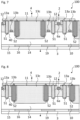
Figure 1 shows a first exemplary embodiment of thesemiconductor device 100 in a cross-sectional view. Thesemiconductor device 100 is, in this case, an RC-IGBT. It comprises asemiconductor body 10 with atop side 11 and abottom side 19, lying opposite to each other in a vertical direction. Thesemiconductor body 10 is based on Si or SiC, for example. - At the
bottom side 19, thesemiconductor body 10 comprises first-type regions 15 and second-type regions 16, which are arranged in an alternating manner. Theregions main electrode 3, namely acollector electrode 3, on thebottom side 19. Thecollector electrode 3 is, for example, formed of metal. - The first-
type regions 15 are of a first conductivity type, which is n-type in the following, and the second-type regions 16 are of a second conductivity type, which is p-type in the following. Adrift region 14 is arranged between thetop side 11 and thebottom side 19. Thedrift region 14 is of the first conductivity type, i.e. n-type. Thedrift region 14 adjoins the first-type 15 and the second-type 16 regions. - A plurality of
trenches semiconductor body 10 and into thedrift region 14. Thetrenches 51 are first-type trenches, herein also called "active trenches", and thetrenches 52 are second-type trenches, herein also called "inactive trenches" or "dummy trenches". - The first-
type trenches 51 are filled with an electrically conductive material which is electrically separated from thesemiconductor body 10 by an electrically insulatinglayer 40, herein called "gate insulation layer". Thus, there is no direct electrical contact between thesemiconductor body 10 and the electrically conductive material in the first-type trenches 51. Thegate insulation layer 40 is, for example, formed of an oxide, like SiO2. The electrically conductive material in the first-type trenches 51 may be a highly-doped polysilicon. The electrically conductive material in the first-type trenches 51 is part of agate electrode 4 of thesemiconductor device 100. - The second-
type trenches 52 are also filled with electrically conductive material, e.g. highly-doped polysilicon, which is also electrically separated from thesemiconductor body 10 by an electrically insulating layer which is the same as thegate insulation layer 40. The electrically conductive material in the second-type trenches 52 is part of a firstmain electrode 2, namely anemitter electrode 2, arranged on thetop side 12. Thefirst base regions 13a adjoin and are in electrical contact with theemitter electrode 2 infirst contact areas 6a, also called "Rb-prime areas". - The
semiconductor body 10 comprisesseveral base regions drift region 14 and thetop side 11. Thebase regions drift region 14 as well as thetop side 11. First 13a and second 13b base regions are shallower (smaller vertical extension) than thetrenches third base region 13c is deeper than thetrenches semiconductor body 10. - As can be seen in
figure 1 , thesemiconductor device 100 is subdivided into a plurality of so-called half-cells. One such half-cell is shown in greater detail infigure 2 . The half-cell is the structure between the vertical dashed lines infigure 2 . Infigure 1 , several such half-cells are arranged one after the other in a first lateral direction, running from the left to the right. Two adjacent half-cells are mirrored with respect to each other at the plane running perpendicularly to the first lateral direction and through thethird base region 13c (see right vertical dashed line infigure 2 ). - As can be seen in
figure 2 , the half-cell comprises a portion (half) of afirst base region 13c, a first-type trench 51, asecond base region 13b, a second-type trench 52 and a portion (half) of athird base region 13c which are arranged one after the other in this order along the first lateral direction. The half-cell further comprises an injection region 12 (source region 12) of the first conductivity type, i.e. n-type, arranged vertically between thefirst base region 13c and thetop side 11. Theinjection region 12 adjoins thefirst base region 13c and the first-type trench 51. Theinjection region 12 further adjoins theemitter electrode 2 and is in electrical contact therewith. - The operation of the semiconductor device may be as follows:
In a so-called transistor mode, theemitter electrode 2 is set to ground and thecollector electrode 3 is set to a positive potential. Thegate electrode 4 is set to a positive potential so that thefirst base region 13a is depleted at the border to the first-type trench 51. A conduction path is created in thefirst base region 13c along the first-type trench 51. Electrons can then be injected from theemitter electrode 2 into theinjection region 12, can travel along the conduction path, and reach into thedrift region 14. On thebottom side 19, holes are injected from thecollector electrode 3 via the second-type regions 16 and also travel into thedrift region 14 so that an electron-hole plasma is created. - When turning off of the transistor mode, the electron-hole plasma can create avalanches in the region of the first-
type trench 51.Figure 17 shows simulations of the current I and the voltage V as a function of time t during turning off from the transistor mode.Figure 18 shows the corresponding simulated maximum avalanche generation I_max as a function of time t. Indeed, during turnoff, there is a very high intensity of avalanches. - Such avalanches can harm the
gate insulation layer 40 so that the long-term performance stability of thesemiconductor device 10 is negatively affected. It has been found that the second-type,inactive trench 52 and thethird base region 13c extending deeper into the semiconductor body than thetrenches active trench 51. - This effect is additionally increased by the second-
type trench 52 extending deeper into the semiconductor body, i.e. having a greater vertical extension, than the first-type trench 51. For example, the depth of the second-type trench 52 is at least 0.5 µm greater than the depth of the first-type trench 51. -
Figure 19 shows simulations of the impact ionization along the cross-sections indicated by the vertical dashed lines infigure 2 . The solid curves A1, A2 and A3 show the impact ionization as a function of the depth Y along the first-type trench 51 and the dashed curves B1, B2, B3 show the impact ionization as a function of the depth Y along the second-type trench 52. - The curves A1 and B1 show simulation results for equal depths of the first-
type trench 51 and the second-type trench 52. The curves A2 and B2 show simulation results for a second-type trench 52 being 1 µm deeper than the first-type trench 51. The curves A3 and B3 show simulation results for the second-type trench 52 being 2 µm deeper than the first-type trench 51. - As can be seen, when the
trenches type trench 52 becoming deeper than the first-type trench 51, the stress on thegate insulation layer 40 in the first-type trench 51 is greatly reduced. The peak of impact ionization at the bottom of the first-type trench 51 is reduced by more than one order of magnitude with a second-type trench 52 which is 1 µm deeper than the first-type trench 51 and by more than two orders of magnitude with a second-type trench 52 which is 2 µm deeper than the first-type trench 51. -
Figure 3 shows a further exemplary embodiment of thesemiconductor device 100 which, in this case, is an IGBT. At thetop side 11, thesemiconductor device 100 is identical to the semiconductor device offigure 1 . Thebottom side 19, however, is only formed by the second-type region 16 (collector layer 16) being of the second conductivity type. -
Figure 4 shows an exemplary embodiment of thesemiconductor device 100 which is a MISFET. Also here, thetop side 11 is the same as infigures 1 and3 . Thebottom side 19, however, is only formed by n-type semiconductor material. - In the exemplary embodiment of the
semiconductor device 100 offigure 5 , not only the depths of the second-type trenches 52 are greater than of the first-type trenches 51, but also the widths measured in the first lateral direction are greater. Trenches with different depths and, at the same time, different widths can be produced particularly easily. - Another exemplary embodiment of the
semiconductor device 100 is shown infigure 6 . In this case, thedrift region 14 comprises afirst drift region 14a and asecond drift region 14b. Thesecond drift region 14b is arranged between thefirst drift region 14a and thebase regions trenches second drift region 14b and end in thefirst drift region 14a. In thesecond drift region 14b, the doping concentration with n-type dopants is greater than in thefirst drift region 14a, e.g. by a factor of at least 10 or at least 100. Such asecond drift region 14b, also called "enhancement region" or "enhancement layer", helps to improve on-state losses. -
Figure 7 to 9 show a further exemplary embodiment of thesemiconductor device 100 in different views. Here, thesecond base regions 13b each comprisesecond contact areas 6b in which thesecond base regions 13b are in electrical contact with the firstmain electrode 2. During turn-off of the transistor mode, at least a part of the plasma can be extracted via thesecontact areas 6b so that the charge carriers are effectively diverted away from the first-type trench 51. As a consequence, the avalanche generation near the first-type trench 51 is further reduced. -
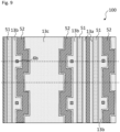
Figure 9 shows thesemiconductor device 100 offigure 7 in top view onto thetop side 11. The upper horizontal dashed line indicates the cross sectional plane for the cross-sectional view offigure 7 . The lower horizontal dashed line indicates the cross-sectional plane for the cross-sectional view offigure 8 . - As can be seen in
figure 9 , the second-type trenches 52 each follow a rectangular function when moving along the second lateral direction. The second lateral direction is from down to up infigure 9 . In each of the rectangles, the distance between the second-type trench 52 and the adjacent first-type trench 51, measured in the first lateral direction, has a maximum value. Within each of the rectangles, acontact area 6b is arranged, in which the respectivesecond base region 13b is in electrical contact with the firstmain electrode 2. In regions where no contact areas are located in thesecond base regions 13b, the distance between the first-type trench 51 and the adjacent second-type trench 52 reaches a minimum value. For example, this minimum value is smaller than the widths of the second-type trenches 52, e.g. is at most 200 nm. -
Figures 10 to 12 show a further exemplary embodiment of thesemiconductor device 100 in the same views as explained in connection withfigures 7 to 9 . Also thethird base regions 13c comprisecontact areas 6c in which thethird base regions 13c are in electrical contact with firstmain electrode 2. Also thesecontact areas 6c can help to divert the plasma away from the first-type trenches 51 during turn-off of the transistor mode. -
Figure 13 shows a further exemplary embodiment of thesemiconductor device 100, now only in top view onto thetop side 11 of thesemiconductor body 10. As can be seen here, the second-type trenches 52 sandwiching thethird base region 13c in the first lateral direction are actually connected at their respective longitudinal ends so that a contiguous trench completely surrounds thefirst base region 13c. -
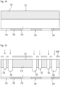
Figure 14 shows a first position in an exemplary embodiment of the method for producing asemiconductor device 100. In this position, asemiconductor body 10 with atop side 11 and abottom side 19 is provided. Thebottom side 19 is formed by first-type regions 15 and second-type regions 16 arranged in an alternating manner. Thetop side 11 is formed by abase region 13 being of the second conductivity type. Adrift region 14 is arranged between thebottom side 19 and thebase region 13, wherein thedrift region 14 is of the first conductivity type. -
Figure 15 shows a position in which trenches are formed in thesemiconductor body 10 by etching into thetop side 11. The trenches are formed with the help of amask 200 which comprises a plurality of holes in the regions where the trenches are to be formed. The holes for the second-type trenches 52 have a greater width than the holes for the first-type trenches 51. Due to this, the trenches are formed with different widths but at the same time also with different depths. -
Figure 16 shows a position after thetrenches trenches semiconductor body 10 by electrically isolatingmaterial 40 arranged in thetrenches first base regions 13a,second base regions 13b andthird base regions 13c have been formed, e.g. by ion implantation. Alsoinjection regions 12 have been formed in thesemiconductor body 10, e.g. by means of ion implantation. - The embodiments shown in the
Figures 1 to 16 as stated represent exemplary embodiments of the improved semiconductor device and the improved method for producing a semiconductor device; therefore, they do not constitute a complete list of all embodiments according to the improved semiconductor device of the improved method. Actual semiconductor devices and methods may vary from the embodiments shown in terms of arrangements, elements and order of method steps, for example. -
- 2
- first main electrode
- 3
- second main electrode
- 4
- gate electrode
- 5
- further electrode
- 6a
- first contact area
- 6b
- second contact area
- 6c
- third contact area
- 10
- semiconductor body
- 11
- top side
- 12
- injection region
- 13
- base region
- 13a
- first base region
- 13b
- second base region
- 13c
- third base region
- 14
- drift region
- 14a
- first drift region
- 14b
- second drift region
- 15
- first-type region
- 16
- second-type region
- 19
- bottom side
- 40
- electrically insulating layer / gate insulation layer
- 51
- first-type trench
- 52
- second-type trench
- 100
- semiconductor device
- 200
- mask
- A1 to A3
- curves
- B1 to B3
- curves
Claims (15)
- Semiconductor device (100) comprising- a semiconductor body (10) extending in vertical direction between a top side (11) and a bottom side (19),- a first main electrode (2) on the top side (11) and a second main electrode (3) on the bottom side (19),- a gate electrode (4),- at least two trenches, namely a first-type trench (51) and a second-type trench (52), each extending from the top side (11) into the semiconductor body (10), wherein- the semiconductor body (10) comprises- a drift region (14) of a first conductivity type vertically between the top side (11) and the bottom side (19),- at least two base regions, namely a first (13a) and a second (13b) base region, each of a second conductivity type and each arranged vertically between the drift region (14) and the top side (11),- an injection region (12) of the first conductivity type vertically spaced apart from the drift region (14) by the first base region (13a) and adjoining the first base region (13a),- the first base region (13a), the first-type trench (51), the second base region (13b) and the second-type trench (52) are arranged in this order one after the other in a first lateral direction,- the first main electrode (2) is in electrical contact with the injection region (12),- the gate electrode (4) extends into the first-type trench (51) where it is separated from the semiconductor body (10) by a gate insulation layer (40),- the second-type trench (52) is free of the gate electrode (4),- the second-type trench (52) extends deeper into the semiconductor body (10) than the first-type trench (51).
- Semiconductor device (100) according to claim 1, wherein- a width of the second-type trench (52) is greater than a width of the first-type trench (51).
- Semiconductor device (100) according to claim 1 or 2, wherein- a minimal distance between the first-type trench (51) and the second-type trench (52), measured in the first lateral direction, is at most 2-times the width of the second-type trench (52).
- Semiconductor device (100) according to claim 1 or 2, wherein- the first main electrode (2) extends into the second-type trench (52) where it is separated from the semiconductor body (10) by an electrically insulating layer (40).
- Semiconductor device (100) according to any one of the preceding claims, wherein- the second base region (13b) comprises at least one contact area (6b) in which the second base region (13b) is in electrical contact with the first main electrode (2).
- Semiconductor device (100) according to claim 5, wherein- the second base region (13b) comprises a plurality of laterally spaced contact areas (6b), wherein the second base region (13b) is in electrical contact with the first main electrode (2) in each of these contact areas (6b).
- Semiconductor device (100) according to claim 6, wherein- the distance between the first-type trench (51) and the second-type trench (52) measured in the first lateral direction varies when moving along a second lateral direction which is perpendicular to the first lateral direction,- the contact areas (6b) in the second base region (13b) are spaced apart from each other in the second lateral direction,- the distance between the first-type trench (51) and the second-type trench is greater where a contact area (6b) is arranged between them and smaller where no contact area is arranged between them.
- Semiconductor device (100) according to any one of the preceding claims, wherein- the second-type trench (52) is arranged between two first-type trenches (51) in the first lateral direction.
- Semiconductor device (100) according to claim 8, wherein- two second-type trenches (52) are arranged between the two first-type trenches (51) in the first lateral direction.
- Semiconductor device (100) according to any one of the preceding claims, wherein- the second-type trench (52) is arranged between the second base region (13b) and a third base region (13c) in the first lateral direction, wherein the third base region (13c) is of the second conductivity type,- the third base region (13c) extends deeper into the semiconductor body (10) than the second-type trench (52).
- Semiconductor device (100) according to claims 9 and 10, wherein- the third base region (13c) is arranged between the two second-type trenches (52) in the first lateral direction,- the third base region (13c) adjoins the two second-type trenches (52),- the two second-type trenches (52) are connected with each other at their respective longitudinal ends so that, in top view onto the top side (11), the third base region (13c) is completely surrounded by a contiguous trench.
- Semiconductor device (100) according to claim 10 or 11, wherein- the third base region (13c) comprises at least one contact area (6c) in which the third base region (13c) is in electrical contact with the first main electrode (2).
- Semiconductor device (100) according to any one of the preceding claims, wherein- the drift region (14) comprises a first drift region (14a) and a second drift region (14b) arranged one after the other in vertical direction,- the second drift region (14b) is arranged vertically between the first drift region (14a) and the first base region (13a),- the second drift region (14b) has a greater doping concentration than the first drift region (14a).
- Method for producing a semiconductor device (100), comprising- providing a semiconductor body (10) with a top side (11) and a bottom side (19),- forming at least two trenches, namely a first-type trench (51) and a second-type trench (52), each one extending from the top side (11) into the semiconductor body (10),- forming a first main electrode (2) on the top side (11) and a second main electrode (3) on the bottom side (19),- forming a gate electrode (4) such that the gate electrode (4) extends into the first-type trench (51) where it is separated from the semiconductor body (10) by a gate insulation layer (40), wherein- the second-type trench (52) is kept free of the gate electrode (4),- the semiconductor device (100) is formed such that the semiconductor body (10) comprises- a drift region (14) of a first conductivity type vertically between the top side (11) and the bottom side (19),- at least two base regions, namely a first (13a) and a second (13b) base region, each of a second conductivity type and each arranged vertically between the drift region (14) and the top side (11),- an injection region (12) of the first conductivity type, vertically spaced apart from the drift region (14) by the first base region (13a) and adjoining the first base region (13a),- the first base region (13a), the first-type trench (51), the second base region (13b) and the second-type trench (52) are arranged in this order one after the other in a first lateral direction,- the first main electrode (2) is in electrical contact with the injection region (12),- the trenches (51, 52) are formed such that the second-type trench (52) extends deeper into the semiconductor body (10) than the first-type trench (51).
- Method according to claim 14, wherein- the trenches (51, 52) are formed in a common etching step using a common mask (200),- the mask (200) comprises holes in the regions where the trenches (51, 52) are to be formed,- the hole for the second-type trench (52) has a greater width than the hole for the first-type-trench (51).
Priority Applications (4)
| Application Number | Priority Date | Filing Date | Title |
|---|---|---|---|
| EP22217357.7A EP4394881B1 (en) | 2022-12-30 | 2022-12-30 | Semiconductor device and method for producing a semiconductor device |
| PCT/EP2023/083588 WO2024141212A1 (en) | 2022-12-30 | 2023-11-29 | Semiconductor device and method for producing a semiconductor device |
| JP2025537626A JP2026500423A (en) | 2022-12-30 | 2023-11-29 | Semiconductor device and manufacturing method thereof |
| CN202380089249.1A CN120435926A (en) | 2022-12-30 | 2023-11-29 | Semiconductor device and method for manufacturing the same |
Applications Claiming Priority (1)
| Application Number | Priority Date | Filing Date | Title |
|---|---|---|---|
| EP22217357.7A EP4394881B1 (en) | 2022-12-30 | 2022-12-30 | Semiconductor device and method for producing a semiconductor device |
Publications (2)
| Publication Number | Publication Date |
|---|---|
| EP4394881A1 true EP4394881A1 (en) | 2024-07-03 |
| EP4394881B1 EP4394881B1 (en) | 2025-07-30 |
Family
ID=84767192
Family Applications (1)
| Application Number | Title | Priority Date | Filing Date |
|---|---|---|---|
| EP22217357.7A Active EP4394881B1 (en) | 2022-12-30 | 2022-12-30 | Semiconductor device and method for producing a semiconductor device |
Country Status (4)
| Country | Link |
|---|---|
| EP (1) | EP4394881B1 (en) |
| JP (1) | JP2026500423A (en) |
| CN (1) | CN120435926A (en) |
| WO (1) | WO2024141212A1 (en) |
Citations (5)
| Publication number | Priority date | Publication date | Assignee | Title |
|---|---|---|---|---|
| US20070114570A1 (en) * | 2002-10-31 | 2007-05-24 | Masakazu Yamaguchi | Power semiconductor device |
| US20080042172A1 (en) * | 2006-08-03 | 2008-02-21 | Infineon Technologies Austria Ag | Semiconductor component having a space saving edge structure |
| US20090283797A1 (en) * | 2008-05-13 | 2009-11-19 | Mitsubishi Electric Corporation | Semiconductor device |
| US20200212209A1 (en) * | 2018-12-26 | 2020-07-02 | Renesas Electronics Corporation | Semiconductor device and method of manufacturing the same |
| EP4016638A1 (en) * | 2020-12-21 | 2022-06-22 | Hitachi Energy Switzerland AG | Power semiconductor device with an insulated trench gate electrode |
Family Cites Families (2)
| Publication number | Priority date | Publication date | Assignee | Title |
|---|---|---|---|---|
| JP5011843B2 (en) * | 2006-06-22 | 2012-08-29 | 株式会社デンソー | Semiconductor device |
| US10636877B2 (en) * | 2016-10-17 | 2020-04-28 | Fuji Electric Co., Ltd. | Semiconductor device |
-
2022
- 2022-12-30 EP EP22217357.7A patent/EP4394881B1/en active Active
-
2023
- 2023-11-29 CN CN202380089249.1A patent/CN120435926A/en active Pending
- 2023-11-29 JP JP2025537626A patent/JP2026500423A/en active Pending
- 2023-11-29 WO PCT/EP2023/083588 patent/WO2024141212A1/en not_active Ceased
Patent Citations (5)
| Publication number | Priority date | Publication date | Assignee | Title |
|---|---|---|---|---|
| US20070114570A1 (en) * | 2002-10-31 | 2007-05-24 | Masakazu Yamaguchi | Power semiconductor device |
| US20080042172A1 (en) * | 2006-08-03 | 2008-02-21 | Infineon Technologies Austria Ag | Semiconductor component having a space saving edge structure |
| US20090283797A1 (en) * | 2008-05-13 | 2009-11-19 | Mitsubishi Electric Corporation | Semiconductor device |
| US20200212209A1 (en) * | 2018-12-26 | 2020-07-02 | Renesas Electronics Corporation | Semiconductor device and method of manufacturing the same |
| EP4016638A1 (en) * | 2020-12-21 | 2022-06-22 | Hitachi Energy Switzerland AG | Power semiconductor device with an insulated trench gate electrode |
Also Published As
| Publication number | Publication date |
|---|---|
| EP4394881B1 (en) | 2025-07-30 |
| WO2024141212A1 (en) | 2024-07-04 |
| JP2026500423A (en) | 2026-01-06 |
| CN120435926A (en) | 2025-08-05 |
Similar Documents
| Publication | Publication Date | Title |
|---|---|---|
| US12057482B2 (en) | MOSFET with distributed doped P-shield zones under trenches | |
| EP0633611B1 (en) | Semiconductor device comprising an insulated-gate bipolar field-effect device | |
| EP2942816B1 (en) | Semiconductor device | |
| CN101308871B (en) | Insulated gate semiconductor device and manufacturing method thereof | |
| EP3659180B1 (en) | Insulated gate power semiconductor device and method for manufacturing such device | |
| US7504307B2 (en) | Semiconductor devices including voltage-sustaining space-charge zone and methods of manufacture thereof | |
| US6784488B2 (en) | Trench-gate semiconductor devices and the manufacture thereof | |
| US20100102381A1 (en) | Power semiconductor device | |
| US7253459B2 (en) | Semiconductor devices and methods of manufacture thereof | |
| TWI685899B (en) | Enhancements to cell layout and fabrication techniques for mos-gated devices | |
| WO2018034818A1 (en) | Power mosfet having planar channel, vertical current path, and top drain electrode | |
| EP4394881B1 (en) | Semiconductor device and method for producing a semiconductor device | |
| US12211903B2 (en) | Semiconductor device and method for designing thereof | |
| EP4394889A1 (en) | Semiconductor device and method for producing a semiconductor device | |
| EP4394888A1 (en) | Semiconductor device and method for producing a semiconductor device | |
| KR102030464B1 (en) | Lateral typed power semiconductor device | |
| EP4203069B1 (en) | Power semiconductor device and manufacturiing method | |
| US12396250B2 (en) | Vertical IGBT with complementary channel for hole extraction | |
| JP2004193630A (en) | High voltage semiconductor device | |
| KR102030466B1 (en) | Lateral typed power semiconductor device | |
| KR101870824B1 (en) | Power semiconductor device and method of fabricating the same | |
| WO2025026593A1 (en) | Vertical semiconductor device with a gate electrode structure having lateral protrusions and method for producing the semiconductor device | |
| CN118538607A (en) | Semiconductor component and method for producing a semiconductor component |
Legal Events
| Date | Code | Title | Description |
|---|---|---|---|
| PUAI | Public reference made under article 153(3) epc to a published international application that has entered the european phase |
Free format text: ORIGINAL CODE: 0009012 |
|
| STAA | Information on the status of an ep patent application or granted ep patent |
Free format text: STATUS: THE APPLICATION HAS BEEN PUBLISHED |
|
| AK | Designated contracting states |
Kind code of ref document: A1 Designated state(s): AL AT BE BG CH CY CZ DE DK EE ES FI FR GB GR HR HU IE IS IT LI LT LU LV MC ME MK MT NL NO PL PT RO RS SE SI SK SM TR |
|
| RIN1 | Information on inventor provided before grant (corrected) |
Inventor name: NIKBERG, BABAK Inventor name: VITALE, WOLFGANG AMADEUS Inventor name: DE MICHIELIS, LUCA Inventor name: BUITRAGO, ELIZABETH |
|
| STAA | Information on the status of an ep patent application or granted ep patent |
Free format text: STATUS: REQUEST FOR EXAMINATION WAS MADE |
|
| 17P | Request for examination filed |
Effective date: 20241120 |
|
| RBV | Designated contracting states (corrected) |
Designated state(s): AL AT BE BG CH CY CZ DE DK EE ES FI FR GB GR HR HU IE IS IT LI LT LU LV MC ME MK MT NL NO PL PT RO RS SE SI SK SM TR |
|
| REG | Reference to a national code |
Ref country code: DE Ref legal event code: R079 Free format text: PREVIOUS MAIN CLASS: H01L0029060000 Ipc: H10D0012010000 Ref country code: DE Ref legal event code: R079 Ref document number: 602022018411 Country of ref document: DE Free format text: PREVIOUS MAIN CLASS: H01L0029060000 Ipc: H10D0012010000 |
|
| RIC1 | Information provided on ipc code assigned before grant |
Ipc: H10D 64/23 20250101ALN20250212BHEP Ipc: H10D 62/13 20250101ALI20250212BHEP Ipc: H10D 62/10 20250101ALI20250212BHEP Ipc: H10D 12/00 20250101ALI20250212BHEP Ipc: H10D 12/01 20250101AFI20250212BHEP |
|
| RIC1 | Information provided on ipc code assigned before grant |
Ipc: H10D 64/23 20250101ALN20250306BHEP Ipc: H10D 62/13 20250101ALI20250306BHEP Ipc: H10D 62/10 20250101ALI20250306BHEP Ipc: H10D 12/00 20250101ALI20250306BHEP Ipc: H10D 12/01 20250101AFI20250306BHEP |
|
| GRAP | Despatch of communication of intention to grant a patent |
Free format text: ORIGINAL CODE: EPIDOSNIGR1 |
|
| STAA | Information on the status of an ep patent application or granted ep patent |
Free format text: STATUS: GRANT OF PATENT IS INTENDED |
|
| INTG | Intention to grant announced |
Effective date: 20250415 |
|
| GRAS | Grant fee paid |
Free format text: ORIGINAL CODE: EPIDOSNIGR3 |
|
| GRAA | (expected) grant |
Free format text: ORIGINAL CODE: 0009210 |
|
| STAA | Information on the status of an ep patent application or granted ep patent |
Free format text: STATUS: THE PATENT HAS BEEN GRANTED |
|
| P01 | Opt-out of the competence of the unified patent court (upc) registered |
Free format text: CASE NUMBER: APP_25520/2025 Effective date: 20250528 |
|
| AK | Designated contracting states |
Kind code of ref document: B1 Designated state(s): AL AT BE BG CH CY CZ DE DK EE ES FI FR GB GR HR HU IE IS IT LI LT LU LV MC ME MK MT NL NO PL PT RO RS SE SI SK SM TR |
|
| REG | Reference to a national code |
Ref country code: GB Ref legal event code: FG4D |
|
| REG | Reference to a national code |
Ref country code: CH Ref legal event code: EP |
|
| REG | Reference to a national code |
Ref country code: DE Ref legal event code: R096 Ref document number: 602022018411 Country of ref document: DE |
|
| REG | Reference to a national code |
Ref country code: IE Ref legal event code: FG4D |
|
| REG | Reference to a national code |
Ref country code: NL Ref legal event code: MP Effective date: 20250730 |
|
| REG | Reference to a national code |
Ref country code: AT Ref legal event code: MK05 Ref document number: 1820579 Country of ref document: AT Kind code of ref document: T Effective date: 20250730 |
|
| PG25 | Lapsed in a contracting state [announced via postgrant information from national office to epo] |
Ref country code: PT Free format text: LAPSE BECAUSE OF FAILURE TO SUBMIT A TRANSLATION OF THE DESCRIPTION OR TO PAY THE FEE WITHIN THE PRESCRIBED TIME-LIMIT Effective date: 20251202 |
|
| PG25 | Lapsed in a contracting state [announced via postgrant information from national office to epo] |
Ref country code: IS Free format text: LAPSE BECAUSE OF FAILURE TO SUBMIT A TRANSLATION OF THE DESCRIPTION OR TO PAY THE FEE WITHIN THE PRESCRIBED TIME-LIMIT Effective date: 20251130 |
|
| PGFP | Annual fee paid to national office [announced via postgrant information from national office to epo] |
Ref country code: DE Payment date: 20251211 Year of fee payment: 4 |
|
| PG25 | Lapsed in a contracting state [announced via postgrant information from national office to epo] |
Ref country code: NO Free format text: LAPSE BECAUSE OF FAILURE TO SUBMIT A TRANSLATION OF THE DESCRIPTION OR TO PAY THE FEE WITHIN THE PRESCRIBED TIME-LIMIT Effective date: 20251030 |
|
| REG | Reference to a national code |
Ref country code: LT Ref legal event code: MG9D |
|
| PG25 | Lapsed in a contracting state [announced via postgrant information from national office to epo] |
Ref country code: AT Free format text: LAPSE BECAUSE OF FAILURE TO SUBMIT A TRANSLATION OF THE DESCRIPTION OR TO PAY THE FEE WITHIN THE PRESCRIBED TIME-LIMIT Effective date: 20250730 |
|
| PG25 | Lapsed in a contracting state [announced via postgrant information from national office to epo] |
Ref country code: FI Free format text: LAPSE BECAUSE OF FAILURE TO SUBMIT A TRANSLATION OF THE DESCRIPTION OR TO PAY THE FEE WITHIN THE PRESCRIBED TIME-LIMIT Effective date: 20250730 |
|
| PG25 | Lapsed in a contracting state [announced via postgrant information from national office to epo] |
Ref country code: HR Free format text: LAPSE BECAUSE OF FAILURE TO SUBMIT A TRANSLATION OF THE DESCRIPTION OR TO PAY THE FEE WITHIN THE PRESCRIBED TIME-LIMIT Effective date: 20250730 Ref country code: NL Free format text: LAPSE BECAUSE OF FAILURE TO SUBMIT A TRANSLATION OF THE DESCRIPTION OR TO PAY THE FEE WITHIN THE PRESCRIBED TIME-LIMIT Effective date: 20250730 |
|
| PG25 | Lapsed in a contracting state [announced via postgrant information from national office to epo] |
Ref country code: GR Free format text: LAPSE BECAUSE OF FAILURE TO SUBMIT A TRANSLATION OF THE DESCRIPTION OR TO PAY THE FEE WITHIN THE PRESCRIBED TIME-LIMIT Effective date: 20251031 |
|
| PG25 | Lapsed in a contracting state [announced via postgrant information from national office to epo] |
Ref country code: SE Free format text: LAPSE BECAUSE OF FAILURE TO SUBMIT A TRANSLATION OF THE DESCRIPTION OR TO PAY THE FEE WITHIN THE PRESCRIBED TIME-LIMIT Effective date: 20250730 |
|
| PG25 | Lapsed in a contracting state [announced via postgrant information from national office to epo] |
Ref country code: LV Free format text: LAPSE BECAUSE OF FAILURE TO SUBMIT A TRANSLATION OF THE DESCRIPTION OR TO PAY THE FEE WITHIN THE PRESCRIBED TIME-LIMIT Effective date: 20250730 |
|
| PG25 | Lapsed in a contracting state [announced via postgrant information from national office to epo] |
Ref country code: PL Free format text: LAPSE BECAUSE OF FAILURE TO SUBMIT A TRANSLATION OF THE DESCRIPTION OR TO PAY THE FEE WITHIN THE PRESCRIBED TIME-LIMIT Effective date: 20250730 Ref country code: BG Free format text: LAPSE BECAUSE OF FAILURE TO SUBMIT A TRANSLATION OF THE DESCRIPTION OR TO PAY THE FEE WITHIN THE PRESCRIBED TIME-LIMIT Effective date: 20250730 |
|
| PG25 | Lapsed in a contracting state [announced via postgrant information from national office to epo] |
Ref country code: RS Free format text: LAPSE BECAUSE OF FAILURE TO SUBMIT A TRANSLATION OF THE DESCRIPTION OR TO PAY THE FEE WITHIN THE PRESCRIBED TIME-LIMIT Effective date: 20251030 |
|
| PG25 | Lapsed in a contracting state [announced via postgrant information from national office to epo] |
Ref country code: ES Free format text: LAPSE BECAUSE OF FAILURE TO SUBMIT A TRANSLATION OF THE DESCRIPTION OR TO PAY THE FEE WITHIN THE PRESCRIBED TIME-LIMIT Effective date: 20250730 |
|
| PG25 | Lapsed in a contracting state [announced via postgrant information from national office to epo] |
Ref country code: RO Free format text: LAPSE BECAUSE OF FAILURE TO SUBMIT A TRANSLATION OF THE DESCRIPTION OR TO PAY THE FEE WITHIN THE PRESCRIBED TIME-LIMIT Effective date: 20250730 |
|
| PG25 | Lapsed in a contracting state [announced via postgrant information from national office to epo] |
Ref country code: SM Free format text: LAPSE BECAUSE OF FAILURE TO SUBMIT A TRANSLATION OF THE DESCRIPTION OR TO PAY THE FEE WITHIN THE PRESCRIBED TIME-LIMIT Effective date: 20250730 |
|
| PG25 | Lapsed in a contracting state [announced via postgrant information from national office to epo] |
Ref country code: DK Free format text: LAPSE BECAUSE OF FAILURE TO SUBMIT A TRANSLATION OF THE DESCRIPTION OR TO PAY THE FEE WITHIN THE PRESCRIBED TIME-LIMIT Effective date: 20250730 |
|
| PG25 | Lapsed in a contracting state [announced via postgrant information from national office to epo] |
Ref country code: IT Free format text: LAPSE BECAUSE OF FAILURE TO SUBMIT A TRANSLATION OF THE DESCRIPTION OR TO PAY THE FEE WITHIN THE PRESCRIBED TIME-LIMIT Effective date: 20250730 |
|
| PG25 | Lapsed in a contracting state [announced via postgrant information from national office to epo] |
Ref country code: CZ Free format text: LAPSE BECAUSE OF FAILURE TO SUBMIT A TRANSLATION OF THE DESCRIPTION OR TO PAY THE FEE WITHIN THE PRESCRIBED TIME-LIMIT Effective date: 20250730 |
|
| PG25 | Lapsed in a contracting state [announced via postgrant information from national office to epo] |
Ref country code: EE Free format text: LAPSE BECAUSE OF FAILURE TO SUBMIT A TRANSLATION OF THE DESCRIPTION OR TO PAY THE FEE WITHIN THE PRESCRIBED TIME-LIMIT Effective date: 20250730 Ref country code: SK Free format text: LAPSE BECAUSE OF FAILURE TO SUBMIT A TRANSLATION OF THE DESCRIPTION OR TO PAY THE FEE WITHIN THE PRESCRIBED TIME-LIMIT Effective date: 20250730 |