EP4394849A1 - Production method for tin-based perovskite layer - Google Patents
Production method for tin-based perovskite layer Download PDFInfo
- Publication number
- EP4394849A1 EP4394849A1 EP22883322.4A EP22883322A EP4394849A1 EP 4394849 A1 EP4394849 A1 EP 4394849A1 EP 22883322 A EP22883322 A EP 22883322A EP 4394849 A1 EP4394849 A1 EP 4394849A1
- Authority
- EP
- European Patent Office
- Prior art keywords
- tin
- based perovskite
- solvent
- dmso
- solution
- Prior art date
- Legal status (The legal status is an assumption and is not a legal conclusion. Google has not performed a legal analysis and makes no representation as to the accuracy of the status listed.)
- Withdrawn
Links
Images



Classifications
-
- C—CHEMISTRY; METALLURGY
- C09—DYES; PAINTS; POLISHES; NATURAL RESINS; ADHESIVES; COMPOSITIONS NOT OTHERWISE PROVIDED FOR; APPLICATIONS OF MATERIALS NOT OTHERWISE PROVIDED FOR
- C09K—MATERIALS FOR MISCELLANEOUS APPLICATIONS, NOT PROVIDED FOR ELSEWHERE
- C09K11/00—Luminescent materials, e.g. electroluminescent or chemiluminescent
- C09K11/02—Use of particular materials as binders, particle coatings or suspension media therefor
-
- H—ELECTRICITY
- H10—SEMICONDUCTOR DEVICES; ELECTRIC SOLID-STATE DEVICES NOT OTHERWISE PROVIDED FOR
- H10K—ORGANIC ELECTRIC SOLID-STATE DEVICES
- H10K30/00—Organic devices sensitive to infrared radiation, light, electromagnetic radiation of shorter wavelength or corpuscular radiation
- H10K30/10—Organic devices sensitive to infrared radiation, light, electromagnetic radiation of shorter wavelength or corpuscular radiation comprising heterojunctions between organic semiconductors and inorganic semiconductors
- H10K30/15—Sensitised wide-bandgap semiconductor devices, e.g. dye-sensitised TiO2
-
- C—CHEMISTRY; METALLURGY
- C01—INORGANIC CHEMISTRY
- C01G—COMPOUNDS CONTAINING METALS NOT COVERED BY SUBCLASSES C01D OR C01F
- C01G19/00—Compounds of tin
- C01G19/04—Halides
-
- B—PERFORMING OPERATIONS; TRANSPORTING
- B05—SPRAYING OR ATOMISING IN GENERAL; APPLYING FLUENT MATERIALS TO SURFACES, IN GENERAL
- B05D—PROCESSES FOR APPLYING FLUENT MATERIALS TO SURFACES, IN GENERAL
- B05D7/00—Processes, other than flocking, specially adapted for applying liquids or other fluent materials to particular surfaces or for applying particular liquids or other fluent materials
- B05D7/24—Processes, other than flocking, specially adapted for applying liquids or other fluent materials to particular surfaces or for applying particular liquids or other fluent materials for applying particular liquids or other fluent materials
-
- C—CHEMISTRY; METALLURGY
- C09—DYES; PAINTS; POLISHES; NATURAL RESINS; ADHESIVES; COMPOSITIONS NOT OTHERWISE PROVIDED FOR; APPLICATIONS OF MATERIALS NOT OTHERWISE PROVIDED FOR
- C09D—COATING COMPOSITIONS, e.g. PAINTS, VARNISHES OR LACQUERS; FILLING PASTES; CHEMICAL PAINT OR INK REMOVERS; INKS; CORRECTING FLUIDS; WOODSTAINS; PASTES OR SOLIDS FOR COLOURING OR PRINTING; USE OF MATERIALS THEREFOR
- C09D11/00—Inks
- C09D11/30—Inkjet printing inks
- C09D11/32—Inkjet printing inks characterised by colouring agents
- C09D11/322—Pigment inks
-
- C—CHEMISTRY; METALLURGY
- C09—DYES; PAINTS; POLISHES; NATURAL RESINS; ADHESIVES; COMPOSITIONS NOT OTHERWISE PROVIDED FOR; APPLICATIONS OF MATERIALS NOT OTHERWISE PROVIDED FOR
- C09D—COATING COMPOSITIONS, e.g. PAINTS, VARNISHES OR LACQUERS; FILLING PASTES; CHEMICAL PAINT OR INK REMOVERS; INKS; CORRECTING FLUIDS; WOODSTAINS; PASTES OR SOLIDS FOR COLOURING OR PRINTING; USE OF MATERIALS THEREFOR
- C09D11/00—Inks
- C09D11/30—Inkjet printing inks
- C09D11/36—Inkjet printing inks based on non-aqueous solvents
-
- C—CHEMISTRY; METALLURGY
- C09—DYES; PAINTS; POLISHES; NATURAL RESINS; ADHESIVES; COMPOSITIONS NOT OTHERWISE PROVIDED FOR; APPLICATIONS OF MATERIALS NOT OTHERWISE PROVIDED FOR
- C09D—COATING COMPOSITIONS, e.g. PAINTS, VARNISHES OR LACQUERS; FILLING PASTES; CHEMICAL PAINT OR INK REMOVERS; INKS; CORRECTING FLUIDS; WOODSTAINS; PASTES OR SOLIDS FOR COLOURING OR PRINTING; USE OF MATERIALS THEREFOR
- C09D7/00—Features of coating compositions, not provided for in group C09D5/00; Processes for incorporating ingredients in coating compositions
- C09D7/20—Diluents or solvents
-
- C—CHEMISTRY; METALLURGY
- C09—DYES; PAINTS; POLISHES; NATURAL RESINS; ADHESIVES; COMPOSITIONS NOT OTHERWISE PROVIDED FOR; APPLICATIONS OF MATERIALS NOT OTHERWISE PROVIDED FOR
- C09D—COATING COMPOSITIONS, e.g. PAINTS, VARNISHES OR LACQUERS; FILLING PASTES; CHEMICAL PAINT OR INK REMOVERS; INKS; CORRECTING FLUIDS; WOODSTAINS; PASTES OR SOLIDS FOR COLOURING OR PRINTING; USE OF MATERIALS THEREFOR
- C09D7/00—Features of coating compositions, not provided for in group C09D5/00; Processes for incorporating ingredients in coating compositions
- C09D7/40—Additives
- C09D7/60—Additives non-macromolecular
- C09D7/61—Additives non-macromolecular inorganic
-
- C—CHEMISTRY; METALLURGY
- C09—DYES; PAINTS; POLISHES; NATURAL RESINS; ADHESIVES; COMPOSITIONS NOT OTHERWISE PROVIDED FOR; APPLICATIONS OF MATERIALS NOT OTHERWISE PROVIDED FOR
- C09K—MATERIALS FOR MISCELLANEOUS APPLICATIONS, NOT PROVIDED FOR ELSEWHERE
- C09K11/00—Luminescent materials, e.g. electroluminescent or chemiluminescent
- C09K11/06—Luminescent materials, e.g. electroluminescent or chemiluminescent containing organic luminescent materials
-
- C—CHEMISTRY; METALLURGY
- C09—DYES; PAINTS; POLISHES; NATURAL RESINS; ADHESIVES; COMPOSITIONS NOT OTHERWISE PROVIDED FOR; APPLICATIONS OF MATERIALS NOT OTHERWISE PROVIDED FOR
- C09K—MATERIALS FOR MISCELLANEOUS APPLICATIONS, NOT PROVIDED FOR ELSEWHERE
- C09K11/00—Luminescent materials, e.g. electroluminescent or chemiluminescent
- C09K11/08—Luminescent materials, e.g. electroluminescent or chemiluminescent containing inorganic luminescent materials
- C09K11/66—Luminescent materials, e.g. electroluminescent or chemiluminescent containing inorganic luminescent materials containing germanium, tin or lead
- C09K11/664—Halogenides
-
- H—ELECTRICITY
- H10—SEMICONDUCTOR DEVICES; ELECTRIC SOLID-STATE DEVICES NOT OTHERWISE PROVIDED FOR
- H10F—INORGANIC SEMICONDUCTOR DEVICES SENSITIVE TO INFRARED RADIATION, LIGHT, ELECTROMAGNETIC RADIATION OF SHORTER WAVELENGTH OR CORPUSCULAR RADIATION
- H10F71/00—Manufacture or treatment of devices covered by this subclass
-
- H—ELECTRICITY
- H10—SEMICONDUCTOR DEVICES; ELECTRIC SOLID-STATE DEVICES NOT OTHERWISE PROVIDED FOR
- H10F—INORGANIC SEMICONDUCTOR DEVICES SENSITIVE TO INFRARED RADIATION, LIGHT, ELECTROMAGNETIC RADIATION OF SHORTER WAVELENGTH OR CORPUSCULAR RADIATION
- H10F77/00—Constructional details of devices covered by this subclass
- H10F77/10—Semiconductor bodies
- H10F77/12—Active materials
-
- H—ELECTRICITY
- H10—SEMICONDUCTOR DEVICES; ELECTRIC SOLID-STATE DEVICES NOT OTHERWISE PROVIDED FOR
- H10K—ORGANIC ELECTRIC SOLID-STATE DEVICES
- H10K30/00—Organic devices sensitive to infrared radiation, light, electromagnetic radiation of shorter wavelength or corpuscular radiation
- H10K30/50—Photovoltaic [PV] devices
-
- H—ELECTRICITY
- H10—SEMICONDUCTOR DEVICES; ELECTRIC SOLID-STATE DEVICES NOT OTHERWISE PROVIDED FOR
- H10K—ORGANIC ELECTRIC SOLID-STATE DEVICES
- H10K71/00—Manufacture or treatment specially adapted for the organic devices covered by this subclass
- H10K71/10—Deposition of organic active material
- H10K71/12—Deposition of organic active material using liquid deposition, e.g. spin coating
- H10K71/13—Deposition of organic active material using liquid deposition, e.g. spin coating using printing techniques, e.g. ink-jet printing or screen printing
- H10K71/135—Deposition of organic active material using liquid deposition, e.g. spin coating using printing techniques, e.g. ink-jet printing or screen printing using ink-jet printing
-
- H—ELECTRICITY
- H10—SEMICONDUCTOR DEVICES; ELECTRIC SOLID-STATE DEVICES NOT OTHERWISE PROVIDED FOR
- H10K—ORGANIC ELECTRIC SOLID-STATE DEVICES
- H10K71/00—Manufacture or treatment specially adapted for the organic devices covered by this subclass
- H10K71/40—Thermal treatment, e.g. annealing in the presence of a solvent vapour
-
- H—ELECTRICITY
- H10—SEMICONDUCTOR DEVICES; ELECTRIC SOLID-STATE DEVICES NOT OTHERWISE PROVIDED FOR
- H10K—ORGANIC ELECTRIC SOLID-STATE DEVICES
- H10K85/00—Organic materials used in the body or electrodes of devices covered by this subclass
- H10K85/50—Organic perovskites; Hybrid organic-inorganic perovskites [HOIP], e.g. CH3NH3PbI3
-
- H—ELECTRICITY
- H10—SEMICONDUCTOR DEVICES; ELECTRIC SOLID-STATE DEVICES NOT OTHERWISE PROVIDED FOR
- H10P—GENERIC PROCESSES OR APPARATUS FOR THE MANUFACTURE OR TREATMENT OF DEVICES COVERED BY CLASS H10
- H10P14/00—Formation of materials, e.g. in the shape of layers or pillars
- H10P14/60—Formation of materials, e.g. in the shape of layers or pillars of insulating materials
- H10P14/63—Formation of materials, e.g. in the shape of layers or pillars of insulating materials characterised by the formation processes
- H10P14/6326—Deposition processes
- H10P14/6342—Liquid deposition, e.g. spin-coating, sol-gel techniques or spray coating
- H10P14/6346—Liquid deposition, e.g. spin-coating, sol-gel techniques or spray coating using printing, e.g. ink-jet printing
-
- H—ELECTRICITY
- H10—SEMICONDUCTOR DEVICES; ELECTRIC SOLID-STATE DEVICES NOT OTHERWISE PROVIDED FOR
- H10P—GENERIC PROCESSES OR APPARATUS FOR THE MANUFACTURE OR TREATMENT OF DEVICES COVERED BY CLASS H10
- H10P14/00—Formation of materials, e.g. in the shape of layers or pillars
- H10P14/60—Formation of materials, e.g. in the shape of layers or pillars of insulating materials
- H10P14/69—Inorganic materials
- H10P14/692—Inorganic materials composed of oxides, glassy oxides or oxide-based glasses
- H10P14/6938—Inorganic materials composed of oxides, glassy oxides or oxide-based glasses the material containing at least one metal element, e.g. metal oxides, metal oxynitrides or metal oxycarbides
- H10P14/69398—Inorganic materials composed of oxides, glassy oxides or oxide-based glasses the material containing at least one metal element, e.g. metal oxides, metal oxynitrides or metal oxycarbides the material having a perovskite structure, e.g. BaTiO3
-
- C—CHEMISTRY; METALLURGY
- C01—INORGANIC CHEMISTRY
- C01P—INDEXING SCHEME RELATING TO STRUCTURAL AND PHYSICAL ASPECTS OF SOLID INORGANIC COMPOUNDS
- C01P2002/00—Crystal-structural characteristics
- C01P2002/30—Three-dimensional structures
- C01P2002/34—Three-dimensional structures perovskite-type (ABO3)
-
- H—ELECTRICITY
- H10—SEMICONDUCTOR DEVICES; ELECTRIC SOLID-STATE DEVICES NOT OTHERWISE PROVIDED FOR
- H10K—ORGANIC ELECTRIC SOLID-STATE DEVICES
- H10K30/00—Organic devices sensitive to infrared radiation, light, electromagnetic radiation of shorter wavelength or corpuscular radiation
- H10K30/40—Organic devices sensitive to infrared radiation, light, electromagnetic radiation of shorter wavelength or corpuscular radiation comprising a p-i-n structure, e.g. having a perovskite absorber between p-type and n-type charge transport layers
-
- Y—GENERAL TAGGING OF NEW TECHNOLOGICAL DEVELOPMENTS; GENERAL TAGGING OF CROSS-SECTIONAL TECHNOLOGIES SPANNING OVER SEVERAL SECTIONS OF THE IPC; TECHNICAL SUBJECTS COVERED BY FORMER USPC CROSS-REFERENCE ART COLLECTIONS [XRACs] AND DIGESTS
- Y02—TECHNOLOGIES OR APPLICATIONS FOR MITIGATION OR ADAPTATION AGAINST CLIMATE CHANGE
- Y02E—REDUCTION OF GREENHOUSE GAS [GHG] EMISSIONS, RELATED TO ENERGY GENERATION, TRANSMISSION OR DISTRIBUTION
- Y02E10/00—Energy generation through renewable energy sources
- Y02E10/50—Photovoltaic [PV] energy
- Y02E10/549—Organic PV cells
Definitions
- the present disclosure relates to a method of producing a tin-based perovskite layer used for solar cells.
- Solar cells that include tin (Sn)-based perovskite layers that replace lead (Pb)-based perovskite layers for light-harvesting layers are proposed (see, e.g. PLT1).
- the solar cells that include the tin-based perovskite layers are considered to be environmentally friendly solar cells.
- divalent tin ions (Sn 2+ ) are easily oxidized to tetravalent tin ions (Sn 4+ ). The oxidization increases the hole density in the layer and decreases the photoelectric conversion efficiency of a solar cell.
- a method of producing a tin-based perovskite layer in PLT1 includes a step of adding a reducing agent to a solution that contains heavy tin halide to prepare a tin-based perovskite precursor solution.
- the reducing agent reduces tin fluoride in the tin-based perovskite precursor solution to tin and does not reduce the heavy tin halide in the tin-based perovskite precursor solution to tin.
- Sn 4+ is less likely to be mixed and the oxidation of Sn 2+ is less likely to occur. Therefore, a significantly good solar cell can be provided.
- PLT1 International Patent Application Laid-Open No. WO2020/175705
- the present disclosure is for solving the above problem, and a main objective of the present disclosure is for providing a method of producing a tin-based perovskite layer in which preparation of a reducing agent is not required and oxidation of divalent tin ions (Sn 2+ ) to tetravalent tin ions (Sn 4+ ) is less likely to occur.
- One aspect of the present disclosure provides a method of producing a thin-based perovskite layer including: a first step for preparing a first solution by dissolving a tin-based perovskite compound in a solvent that does not contain dimethyl sulfoxide (DMSO); a third step for applying the first solution to a base after the first step; and a second step for mixing DMSO with the first solution after the first step and a predetermined time before the third step.
- DMSO dimethyl sulfoxide
- the first solution is prepared by dissolving the tin-based perovskite compound in the solvent that does not contain dimethyl sulfoxide (DMSO).
- the first solution is applied to the base after the first step.
- DMSO divalent tin ions
- Sn 4+ tetravalent tin ions
- DMSO is mixed with the first solution after the first step and the predetermined time before the third step.
- timing of the mixing of DMSO is delayed and thus the oxidation of Sn 2+ to Sn 4+ is less likely to occur.
- the mixture of DMSO during the production of the tin-based perovskite layer promotes the crystallization of the tin-based perovskite layer.
- DMSO is mixed with the first solution in the second step immediately before the third step. According to the step, the timing of the mixing of DMSO is the latest and thus the oxidation of Sn 2+ to Sn 4+ is further less likely to occur.
- the first solution is prepared in the first step by mixing the tin-based perovskite compound with the solution that does not contain DMSO and stirring mixture of the tin-based perovskite compound and the solvent to dissolve the tin-based perovskite compound in the solvent.
- the first solution is prepared in the first step by mixing the tin-based perovskite compound with the solvent that does not contain DMSO and stirring mixture of the tin-based perovskite compound and the solvent for 10 hours or more to dissolve the tin-based perovskite compound in the solvent.
- the first solvent prepared by dissolving the perovskite compound in the solvent that does not contain DMSO is nearly homogeneous.
- the first solution is prepared in the first step by mixing the tin-based perovskite compound with the solvent that does not contain DMSO and stirring mixture of the tin-based perovskite compound and the solvent for 24 hours or more to dissolve the tin-based perovskite compound in the solvent.
- the first solvent prepared by dissolving the perovskite compound in the solvent that does not contain DMSO is further nearly homogeneous.
- the tin-based perovskite layer is represented by general formula ASnX 3 , where A is at least one of an alkali metal ion, a rubidium ion, a methylammonium ion, an ethylammonium ion, a formamidium ion, a guanidium ion, and an alkylammonium ion, and X is at least one of Group VII elements including fluorine (F), chlorine (CL), bromine (Br), and iodine (I).
- the first solution contains SnI 2 , SnF 2 , and MAI as solutes and DMF as a solvent.
- a production device 100 includes a first container 11, a first pump 13, a first solenoid valve 15, a second container 21, a second pump 23, a second solenoid valve 25, a mixer 30, a third pump 33, a third solenoid valve 35, a buffer tank 40, a fourth pump 42, and an inkjet printer 44.
- the buffer tank 40 holds the precursor solution L3 supplied from the mixer 30 via the third solenoid valve 35.
- the buffer tank 40 has a holding capacity that is sufficient for stably supplying the precursor solution L4 to the inkjet printer 44 that continuously discharges the precursor solution L4 for a certain period of time.
- Chlorobenzene which is a poor solvent, is dropped onto the precursor solution L4 on the base S and then the precursor solution L4 is heated and dried (an annealing step, a heating step) to form the perovskite layer.
- the heating temperature may be 20 °C to 300 °C, preferably 50 °C to 170 °C.
- a three-dimensional crystal structure (a perovskite structure) begins to form.
- the three-dimensional structure crystal is MASnI 3 (CH 3 NH 3 SnI 3 ).
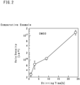
- a graph in FIG. 2 illustrates a relationship between stirring time and hole density in a comparative example that includes a solvent that contains only DMSO.
- the solvent that dissolve the tin-based perovskite compound is prepared from only DMSO and used to produce the tin-based perovskite layer.
- the hole density increases as a period of time in which the raw material liquid that consists of DMSO, SnI 2 , and MAI is stirred increases. This is because the DMSO oxidizes divalent tin ions (Sn 2+ ) to tetravalent tin ions (Sn 4+ ).
- the photoelectric conversion efficiency of the tin-based perovskite layer decreases.
- a graph in FIG. 3 illustrates relationships between output voltage [V] and current density [mA/cm 2 ] with stirring time of 1 hour and with stirring time of 24 hours in the comparative example. With the stirring time of 24 hours, the current density is low in comparison to the current density with the stirring time of 1 hour.
- the buffer tank 40 and the fourth pump 42 may be removed from the tin-based perovskite layer production device 100 as illustrated in FIG. 6 .
- the holding capacity of the mixer 30 may be set equal to or greater than the holding capacity of the buffer tank 40.
Landscapes
- Chemical & Material Sciences (AREA)
- Engineering & Computer Science (AREA)
- Materials Engineering (AREA)
- Organic Chemistry (AREA)
- Wood Science & Technology (AREA)
- Life Sciences & Earth Sciences (AREA)
- Inorganic Chemistry (AREA)
- Manufacturing & Machinery (AREA)
- Physics & Mathematics (AREA)
- Electromagnetism (AREA)
- Photovoltaic Devices (AREA)
- Application Of Or Painting With Fluid Materials (AREA)
- Liquid Deposition Of Substances Of Which Semiconductor Devices Are Composed (AREA)
Abstract
Description
- The present application is based on
Japanese Patent Application No. 2021-170558 filed on October 18, 2021 - The present disclosure relates to a method of producing a tin-based perovskite layer used for solar cells.
- Solar cells that include tin (Sn)-based perovskite layers that replace lead (Pb)-based perovskite layers for light-harvesting layers are proposed (see, e.g. PLT1). The solar cells that include the tin-based perovskite layers are considered to be environmentally friendly solar cells. In a tin-based perovskite material, divalent tin ions (Sn2+) are easily oxidized to tetravalent tin ions (Sn4+). The oxidization increases the hole density in the layer and decreases the photoelectric conversion efficiency of a solar cell. A method of producing a tin-based perovskite layer in PLT1 includes a step of adding a reducing agent to a solution that contains heavy tin halide to prepare a tin-based perovskite precursor solution. The reducing agent reduces tin fluoride in the tin-based perovskite precursor solution to tin and does not reduce the heavy tin halide in the tin-based perovskite precursor solution to tin. According to the method, Sn4+ is less likely to be mixed and the oxidation of Sn2+ is less likely to occur. Therefore, a significantly good solar cell can be provided.
- PLT1: International Patent Application Laid-Open No.
WO2020/175705 - The method described in PLT1 requires the preparation of the reducing agent, that is, an extra step. Further, the method requires determination of an optimal amount of the reducing agent to be added.
- The present disclosure is for solving the above problem, and a main objective of the present disclosure is for providing a method of producing a tin-based perovskite layer in which preparation of a reducing agent is not required and oxidation of divalent tin ions (Sn2+) to tetravalent tin ions (Sn4+) is less likely to occur.
- One aspect of the present disclosure provides a method of producing a thin-based perovskite layer including: a first step for preparing a first solution by dissolving a tin-based perovskite compound in a solvent that does not contain dimethyl sulfoxide (DMSO); a third step for applying the first solution to a base after the first step; and a second step for mixing DMSO with the first solution after the first step and a predetermined time before the third step.
- According to the steps, in the first step, the first solution is prepared by dissolving the tin-based perovskite compound in the solvent that does not contain dimethyl sulfoxide (DMSO). In the third step, the first solution is applied to the base after the first step. The mixing of DMSO during the production of the tin-based perovskite layer is effective for promoting crystallization of the tin-based perovskite layer. However, the discloser of the present application focused on the fact that DMSO oxidizes divalent tin ions (Sn2+) to tetravalent tin ions (Sn4+) and reduces the photoelectric conversion efficiency of the tin-based perovskite layer.
- In the second step, DMSO is mixed with the first solution after the first step and the predetermined time before the third step. In comparison to a first step in which DMSO is mixed, timing of the mixing of DMSO is delayed and thus the oxidation of Sn2+ to Sn4+ is less likely to occur. Further, the mixture of DMSO during the production of the tin-based perovskite layer promotes the crystallization of the tin-based perovskite layer.
- In a second aspect, the predetermined time is less than 2 hours. In a third aspect, the predetermined time is less than 1 hour. In a fourth aspect, the predetermined time is less than 5 minutes. According to the steps, the timing of the mixing of DMSO is further delayed and thus the oxidation of Sn2+ to Sn4+ is further less likely to occur.
- In a fifth aspect, DMSO is mixed with the first solution in the second step immediately before the third step. According to the step, the timing of the mixing of DMSO is the latest and thus the oxidation of Sn2+ to Sn4+ is further less likely to occur.
- Specifically, as in a sixth aspect, the first solution is prepared in the first step by mixing the tin-based perovskite compound with the solution that does not contain DMSO and stirring mixture of the tin-based perovskite compound and the solvent to dissolve the tin-based perovskite compound in the solvent.
- In a seventh aspect, the first solution is prepared in the first step by mixing the tin-based perovskite compound with the solvent that does not contain DMSO and stirring mixture of the tin-based perovskite compound and the solvent for 10 hours or more to dissolve the tin-based perovskite compound in the solvent. According to the step, the first solvent prepared by dissolving the perovskite compound in the solvent that does not contain DMSO is nearly homogeneous.
- In an eighth aspect, the first solution is prepared in the first step by mixing the tin-based perovskite compound with the solvent that does not contain DMSO and stirring mixture of the tin-based perovskite compound and the solvent for 24 hours or more to dissolve the tin-based perovskite compound in the solvent. According to the step, the first solvent prepared by dissolving the perovskite compound in the solvent that does not contain DMSO is further nearly homogeneous.
- In a ninth aspect, the first solution is stirred after DMSO is mixed with the first solution in the second step. According to the step, DMSO is less likely to be uneven in the first solution.
- Specifically, as in a tenth aspect, the tin-based perovskite layer is represented by general formula ASnX3, where A is at least one of an alkali metal ion, a rubidium ion, a methylammonium ion, an ethylammonium ion, a formamidium ion, a guanidium ion, and an alkylammonium ion, and X is at least one of Group VII elements including fluorine (F), chlorine (CL), bromine (Br), and iodine (I).
- Specifically as in an eleventh aspect, for an iodine ion (I-), a fluorine ion (F-), a methylammonium ion (MA+), and dimethylformamide (DMF), the first solution contains SnI2, SnF2, and MAI as solutes and DMF as a solvent.
- In a twelfth aspect, for formamidium ions (FA+), the first solution further contains FAI as a solute. According to the step, the quality of the tin-based perovskite layer can be further improved.
- The above and other objects, features, and advantages of the present disclosure will be apparent from the following detailed description made with reference to the accompanying drawings.
- [
FIG. 1 ] A schematic view of a device for producing a tin-based perovskite layer. - [
FIG. 2 ] A graph illustrating a relationship between stirring time and hole density in a comparative example that includes a solvent that contains only dimethyl sulfoxide (DMSO). - [
FIG. 3 ] A graph illustrating relationships between output voltage and current density with stirring time of 1 hour and with stirring time of 24 hours in the comparative example. - [
FIG. 4 ] A graph illustrating relationships between external quantum efficiency and short-circuit current density with respect to wavelength with stirring time of 1 hour and with stirring time of 24 hours in the comparative example. - [
FIG. 5 ] A graph illustrating a relationship between stirring time and hole density in the comparative example that includes a solvent that contains dimethylformamide (DMF) and DMSO with a ratio of 4:1. - [
FIG. 6 ] A schematic view of a modification of the device for producing a tin-based perovskite layer. - [
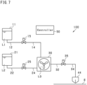
FIG. 7 ] A schematic view of another modification of the device for producing a tin-based perovskite layer. - An embodiment including a device for producing a tin-based perovskite layer used in a tin-based perovskite solar cell will be described with reference to the drawings.
- As illustrated in
FIG. 1 , aproduction device 100 includes afirst container 11, afirst pump 13, afirst solenoid valve 15, asecond container 21, asecond pump 23, asecond solenoid valve 25, amixer 30, athird pump 33, athird solenoid valve 35, abuffer tank 40, afourth pump 42, and aninkjet printer 44. - The
first container 11 holds a first raw material liquid L1 (a first solution). The first raw material liquid L1 contains dimethylformamide (DMF), stannous iodide (SnI2), stannous fluoride (SnF2), and methylammonium iodide (MAI) for DMF, tin ions (Sn2+), iodine ions (I-), fluorine ions (F-), and methylammonium ions (MA+), and does not contain dimethyl sulfoxide (DMSO). The first raw material liquid L1 is stirred for 24 hours (10 hours or more, 24 hours or more) before being stored in thefirst container 11. - SnI2, SnF2, and MAI are raw materials of a tin-based perovskite compound. A material represented by general formula ASnX3 may be used for the tin-based perovskite compound. The first row material liquid L1 may use raw materials represented by general formula AX and general formula SnX2 for the perovskite compound. Here, A may be at least one of an alkali metal ion, a rubidium ion, a methylammonium ion, an ethylammonium ion, a formamidium ion, a guanidium ion, and an alkylammonium ion. X may be at least one of Group VII elements including fluorine (F), chlorine (CL), bromine (Br), and iodine (I).
- In the first raw material liquid L1, a molar ratio of AX and SnX2 is adjusted based on the target characteristics of the perovskite layer. When forming a perovskite compound for a light absorber, a preferably molar ratio of AX and SnX2 may be 1:10 to 10:1.
- DMF may be a solvent that does not contain DMSO. The solvent that does not contain DMSO is not limited as long as it can dissolve AX and SnX2 described above; however, a polar solvent may be preferable. Specifically, γ-butyrolactone, N-methyl-2-pyrrolidone, N,N-dimethylformamide, isopropanol, sulfolane, propylene carbonate, ethylcyanoacetate, acetyl acetone, cyclopentanone, cyclohexanone, cycloheptane, aniline, piperidine, pyridine, cyclooctanone, tetrahydrofurfuryl acetate, cyclohexyl acetate, cyclopentyl methyl ether, phenylethylamine, ethlenediamine, trimethylamine, diisopropylethylamine, or hydrazine may be used.
- The
first pump 13 is connected to thefirst container 11 via aflow channel 12. Themixer 30 is connected to thefirst pump 13 via aflow channel 14. Thefirst solenoid valve 15 is disposed in theflow channel 14. Thefirst pump 13 sucks the first raw material liquid L1 from thefirst container 11 and discharges the first raw material liquid L1 to thefirst solenoid valve 15. Thefirst solenoid valve 15 allows and blocks a supply of the first raw material liquid L1, which is discharged by thefirst pump 13, to themixer 30. Thefirst pump 13 and thefirst solenoid valve 15 are controlled by acontroller 50. - The
second container 21 holds a second raw material liquid L2. The second raw material liquid L2 contains DMSO. Thesecond pump 23 is connected to thesecond container 21 via aflow channel 22. Themixer 30 is connected to thesecond pump 23 via aflow channel 24. Thesecond solenoid valve 25 is disposed in theflow channel 24. Thesecond pump 23 sucks the second raw material liquid L2 from thesecond container 21 and discharges the second raw material liquid L2 to thesecond solenoid valve 25. Thesecond solenoid valve 25 allows and blocks a supply of the second raw material liquid L2, which is discharged by thesecond pump 23, to themixer 30. Thesecond pump 23 and thesecond solenoid valve 25 are controlled by thecontroller 50. - The
mixer 30 holds the first raw material liquid L1 supplied via thefirst solenoid valve 15 and the second raw material liquid L2 supplied via thesecond solenoid valve 25. Themixer 30 stirs the first raw material liquid L1 and the second raw material liquid L2 in themixer 30. Namely, themixer 30 functions as a tank for storing the first raw material liquid L1 and the second raw material liquid L2. Further, themixer 30 functions as a stirrer for stirring the first raw material liquid L1 and the second raw material liquid L2 in themixer 30. Through the stirring of the first raw material liquid L1 and the second raw material liquid L2 by themixer 30, a precursor solution L3 (a solution) in which a tin-based perovskite compound is dissolved in a solvent is prepared. Themixer 30 is controlled by thecontroller 50. - The
third pump 33 is connected to themixer 30 via aflow channel 32. Thebuffer tank 40 is connected to thethird pump 33 via aflow channel 34. Thethird solenoid valve 35 is disposed in theflow channel 34. Thethird pump 33 sucks the precursor solution L3 from themixer 30 and discharges the precursor solution L3 to thethird solenoid valve 35. Thethird solenoid valve 35 allows and blocks a supply of the precursor solution L3 discharged by thethird pump 33 to thebuffer tank 40. Thethird pump 33 and thethird solenoid valve 35 are controlled by thecontroller 50. - The
buffer tank 40 holds the precursor solution L3 supplied from themixer 30 via thethird solenoid valve 35. Thebuffer tank 40 has a holding capacity that is sufficient for stably supplying the precursor solution L4 to theinkjet printer 44 that continuously discharges the precursor solution L4 for a certain period of time. - The
fourth pump 42 is connected to thebuffer tank 40 via aflow channel 41. Theinkjet printer 44 is connected to thefourth pump 42 via aflow channel 43. Thefourth pump 42 sucks the precursor solution L4 from thebuffer tank 40 and discharges the precursor solution L4 to theinkjet printer 44. Thefourth pump 42 is controlled by thecontroller 50. - The inkjet printer 44 (a discharger) discharges the precursor solution L4 supplied from the
buffer tank 40 onto a base S. Namely, theinkjet printer 44 applies the precursor solution L4 to the base S. Theinkjet printer 44 is controlled by thecontroller 50. The base S includes a substrate (e.g., a glass substrate, a flexible substrate) on which a transparent conductive layer and an electron transport layer or a hole transport layer are formed in this sequence from the substrate side. Theinkjet printer 44 may be replaced with a slot die, a spin coater, or a roll coater. - Chlorobenzene, which is a poor solvent, is dropped onto the precursor solution L4 on the base S and then the precursor solution L4 is heated and dried (an annealing step, a heating step) to form the perovskite layer. The heating temperature may be 20 °C to 300 °C, preferably 50 °C to 170 °C. When the precursor solution L4 is heated, a three-dimensional crystal structure (a perovskite structure) begins to form. In this embodiment, the three-dimensional structure crystal is MASnI3 (CH3NH3SnI3).
- The thickness of the perovskite layer is preferably 10 to 5000 [nm], more preferably 100 to 1000 [nm], so that the photoelectric conversion efficiency is more likely to improve even in low temperature (200 °C or less) processing. A hole transport layer or an electron transport layer and an electrode are layered on the perovskite layer.
- The
control unit 50 includes at least a CPU, a ROM, a RAM, and an input/output interface. Thecontrol unit 50 controls thefirst pump 13, thefirst solenoid valve 15, thesecond pump 23, thesecond solenoid valve 25, themixer 30, thethird pump 33, thethird solenoid valve 35, thefourth pump 42, and theinkjet printer 44. - Next, a method of producing the tin-based perovskite layer will be described.
- The first raw material liquid L1 is stirred for 24 hours (10 hours or more, 24 hours or more) by a stirrer, which is not illustrated (a first step). The stirrer may be controlled by the
controller 50 or by another controller, or manually operated by an operator. Then, the first raw material liquid L1 that is stirred is supplied to thefirst container 11. - The
controller 50 controls thefirst pump 13 to discharge the first raw material liquid L1 to thefirst solenoid valve 15 and controls thefirst solenoid valve 15 to supply the first raw material liquid L1 to themixer 30. - The
controller 50 controls thesecond pump 23 to discharge the second raw material liquid L2 to thesecond solenoid valve 25 and then controls thesecond solenoid valve 25 to supply the second raw material liquid L2 to themixer 30. Namely, after the first raw material liquid L1 that is stirred in advance is supplied to themixer 30 via thefirst solenoid valve 15, the second raw material liquid L2 is supplied to themixer 30 via the second solenoid valve 25 (a second step). - The
controller 50 controls themixer 30 to stir the first raw material liquid L1 and the second raw material liquid L2 in themixer 30 for one minute (or quickly stir them). Through the steps, the precursor solution L3 is prepared. - The
controller 50 controls thethird pump 33 to discharge the precursor solution L3 to thethird solenoid valve 35 and then controls thethird solenoid valve 35 to supply the precursor solution L3 to thebuffer tank 40. Namely, thecontroller 50 controls thethird solenoid valve 35 to supply the precursor solution L3 to thebuffer tank 40 after the first raw material liquid L1 and the second raw material liquid L2 in themixer 30 are stirred. - The
controller 50 controls thefourth pump 42 to discharge the precursor solution L4 in thebuffer tank 40 to theinkjet printer 44. - The
controller 50 controls theinkjet printer 44 to discharge the precursor solution L4 supplied from thebuffer tank 40 onto the base S (a third step). After the first raw material liquid L1 is stirred and a predetermined period of time before the precursor solution L4 supplied from thebuffer tank 40 is discharged to the base S via theinkjet printer 44, thecontroller 50 controls thesecond solenoid valve 25 to supply the second raw material liquid L2 to themixer 30. The predetermined period of time may be less than 2 hours, preferably less than 1 hour, and more preferably less than 5 minutes. - A graph in
FIG. 2 illustrates a relationship between stirring time and hole density in a comparative example that includes a solvent that contains only DMSO. - The solvent that dissolve the tin-based perovskite compound is prepared from only DMSO and used to produce the tin-based perovskite layer. In such a tin-based perovskite layer, the hole density increases as a period of time in which the raw material liquid that consists of DMSO, SnI2, and MAI is stirred increases. This is because the DMSO oxidizes divalent tin ions (Sn2+) to tetravalent tin ions (Sn4+). As the hole density of the tin-based perovskite layer increases, the photoelectric conversion efficiency of the tin-based perovskite layer decreases.
- A graph in
FIG. 3 illustrates relationships between output voltage [V] and current density [mA/cm2] with stirring time of 1 hour and with stirring time of 24 hours in the comparative example. With the stirring time of 24 hours, the current density is low in comparison to the current density with the stirring time of 1 hour. - A graph in
FIG. 4 illustrates relationships between external quantum efficiency (EQE) and short-circuit current density (Jsc) with respect to wavelength with stirring time of 1 hour and with stirring time of 24 hours in the comparative example. With the stirring time of 24 hours, the external quantum efficiency (EQE) and the short-circuit current density (Jsc) are low in comparison to those with the stirring time of 1 hour. - A graph in
FIG. 5 illustrates a relationship between stirring time and hole density in the comparative example that uses a solvent that contains DMF and DMSO with a ratio of 4:1. - The hole density of the tin-based perovskite layer produced using the solvent that contains DMF and DMSO with the ratio of 4:1 for dissolving the tin-based perovskite compound increases as the stirring time of the raw material liquid that contains DMF, DMSO, SnI2, SnF2, and MAI increases. In the comparative example, DMSO also oxidizes divalent tin ions (Sn2+) to tetravalent tin ions (Sn4+).
- The mixing of DMSO during the production of the tin-based perovskite layer is effective for promoting crystallization of the tin-based perovskite layer. To suppress the oxidation of Sn2+ to Sn4+, in the method of producing the tin-based perovskite layer described above, the first raw material liquid L1 that has been stirred in advance is supplied to the
mixer 30 via thefirst solenoid valve 15 and then the second raw material liquid L2 is supplied to themixer 30 via thesecond solenoid valve 25. Further, after the first raw material liquid L1 is stirred and the predetermined period of time before the precursor solution L4 supplied from thebuffer tank 40 is discharged to the base S via theinkjet printer 44, thecontroller 50 controls thesecond solenoid valve 25 to supply the second raw material liquid L2 to themixer 30. - The photoelectric conversion efficiency of the tin-based perovskite layer in the comparative example produced by simultaneously supplying the first raw material liquid L1 and the second raw material liquid L2 to the
mixer 30 and then stirring them by themixer 30 for 24 hours was 2.9%. The photoelectric conversion efficiency of the tin-based perovskite layer in this embodiment produced by supplying the first raw material liquid L1 that has been stirred for 24 hours in advance to themixer 30, then supplying the second raw material liquid L2 to themixer 30, and stirring them for one minute (or quickly stirring them) was 6.4%. By reducing the time from when DMSO is added after the first raw material liquid L1 is stirred to when the precursor solution L4 is discharged by theinkjet printer 44, the oxidation of Sn2+ to Sn4+ is less likely to occur. - The embodiment described in detail above has the following advantages.
- In the second step, DMSO is mixed with the precursor solution L3 after the first step and the predetermined time before the third step. Specifically, after the first raw material liquid L1 that has been stirred in advance is supplied to the
mixer 30 via thefirst solenoid valve 15 and the predetermined time before the precursor solution L4 that is supplied from thebuffer tank 40 is discharged onto the base S via theinkjet printer 44, thecontroller 50 controls thesecond solenoid valve 25 to supply the second raw material liquid L2 to themixer 30. In comparison to the method in which the DMSO is mixed in the first step, the timing of the mixing of DMSO is delayed and thus the oxidation of Sn2+ to Sn4+ by DMSO is less likely to occur. According to the method, the oxidation of Sn2+ to Sn4+ can be suppressed without an additional reducing agent. Further, DMSO is mixed during the production of the tin-based perovskite layer. This promotes the crystallization of the tin-based perovskite layer. - The predetermined time is less than 2 hours. The predetermine time is preferably less than 1 hour and more preferably less than 5 minutes. According to the steps, the timing of the mixing of DMSO is delayed, and thus the oxidation of Sn2+ to Sn4+ is less likely to occur.
- In the first step, the first raw material liquid L1 is prepared by mixing the tin-based perovskite compound with the solvent that does not contain DMSO and dissolving the perovskite compound by stirring for 24 hours (10 hours or more, 24 hours or more). The first raw material liquid L1 prepared by dissolving the perovskite compound in the solvent that does not contain DMSO through this step is nearly homogeneous.
- In the second step, the first raw material liquid L1 is stirred after DMSO is mixed with the first raw material liquid L1. Specifically, after the second raw material liquid L2 is supplied to the
mixer 30 via thesecond solenoid valve 25 and the first raw material liquid L1 and the second raw material li1uid L2 are stirred by themixer 30, thecontroller 50 controls thethird solenoid valve 35 to supply the precursor solution L3 to thebuffer tank 40. According to the step, DMSO is less likely to be uneven in the precursor solution L3. - The
first solenoid valve 15 allows and blocks the supply of the first raw material liquid L1 prepared by mixing the tin-based perovskite compound with the solvent that does not contain DMSO. The supply of the first raw material liquid L1 that has been stirred in advance can be allowed by thefirst solenoid valve 15. - The
second solenoid valve 25 allows and blocks the supply of DMSO, that is, the second raw material liquid L2. Themixer 30 holds the first raw material liquid L1 supplied via thefirst solenoid valve 15 and the second raw material liquid L2 supplied via thesecond solenoid valve 25 and stirs them. Thecontroller 50 controls thefirst solenoid valve 15, thesecond solenoid valve 25, and themixer 30. Through the control of thefirst solenoid valve 15 and thesecond solenoid valve 25 by thecontroller 50, the first raw material liquid L1 and the second raw material liquid L2 are supplied to themixer 30. Further, through the control of themixer 30 by thecontroller 50, the first raw material liquid L1 and the second raw material liquid L2 in themixer 30 are stirred. - Through the control of the
first solenoid valve 15 and thesecond solenoid valve 25 by thecontroller 50, the timing of the supply of the first raw material liquid L1 to themixer 30 and the timing of the supply of the second raw material liquid L2 to themixer 30 can be controlled. The timing of the supply of the second raw material liquid L2 to themixer 30 can be delayed relative to the timing of the supply of the first raw material liquid L1 to themixer 30. Thecontroller 50 then controls themixer 30 to stir the first raw material liquid L1 and the second raw material liquid L2 in themixer 30. Therefore, the oxidation of Sn2+ to Sn4+ can be suppressed without an additional reducing agent. Further, the mixing of DMSO during the production of the tin-based perovskite layer promotes the crystallization of the tin-based perovskite layer. The precursor solution L3 supplied from themixer 30 can be supplied to thebuffer tank 40 via thethird solenoid valve 35. - The
buffer tank 40 holds the precursor solution L3 supplied from themixer 30 via thethird solenoid valve 35. The precursor solution L3 can be temporarily stored in thebuffer tank 40 and thus precursor solution L3 can be stably supplied to theinkjet printer 44. Further, thecontroller 50 can control theinkjet printer 44 to discharge the precursor solution L4 supplied from thebuffer tank 40 to the base S. - The
controller 50 controls thesecond pump 23 to discharge the second raw material liquid L2 to thesecond solenoid valve 25 and then control thesecond solenoid valve 25 to supply the second raw material liquid L2 to themixer 30 after the control of thefirst pump 13 to discharge the first raw material liquid L1 to thefirst solenoid valve 15 and the control of thefirst solenoid valve 15 to supply the first raw material liquid L1 to themixer 30. According to the configuration, the timing of the supply of the second raw material liquid L2 to themixer 30 can be delayed relative to the timing of the supply of the first raw material liquid L1 to themixer 30. - The second raw material liquid L2 can be supplied to the
mixer 30 after the first raw material liquid L1 that has been stirred in advance is supplied to themixer 30. Therefore, a second raw material (i.e., DMSO) can be added after the tin-based perovskite compound is dissolved in the solvent that does not contain DMSO in advance. Therefore, the oxidation of Sn2+ to Sn4+ is further less likely to occur. - The precursor solution L3 can be supplied to the
third solenoid 35 after the first raw material liquid L1 and the second raw material liquid L2 in themixer 30 are stirred. Therefore, the tin-based perovskite compound can be more easily dissolved in DMSO that is added later. - The embodiment described above may be modified and implemented as follows. Components that are the same as those in the embodiment described above may be denoted by the reference signs of the corresponding components and will not be described.
- For formamidium ions (FA+), formamidium iodide (FAI) may be contained in the first raw material liquid L1 (or the precursor solution L3) as a solute. The photoelectric conversion efficiency of the tin-based perovskite layer of the comparative example that was produced by simultaneously supplying the first raw material liquid L1 and the second raw material liquid L2 to the
mixer 30 and stirring them by themixer 30 for 24 hours was 4.6%. The photoelectric conversion efficiency of the tin-based perovskite layer of the embodiment produced by supplying the first raw material liquid L1 that has been stirred for 24 hours to themixer 30 and then supplying the second raw material liquid L2 to themixer 30 and stirring them for one minute (or quickly stir them) was 9.5%. By reducing the time from when DMSO is added after the first raw material liquid L1 that contains FAI is stirred to when the precursor solution L4 is discharged via theinkjet printer 44, the oxidation of Sn2+ to Sn4+ is less likely to occur. - In the second step, DMSO may be mixed with the precursor solution L3 immediately before the third step. According to the method, the timing of the mixing of DMSO can be delayed and thus the oxidation of Sn2+ to Sn4+ by DMSO is further less likely to occur.
- The
buffer tank 40 and thefourth pump 42 may be removed from the tin-based perovskitelayer production device 100 as illustrated inFIG. 6 . In this configuration, the holding capacity of themixer 30 may be set equal to or greater than the holding capacity of thebuffer tank 40. - The
first pump 13, thesecond pump 23, and thethird pump 33 may be removed from the tin-based perovskitelayer production device 100 inFIG. 6 as illustrated inFIG. 7 . In this configuration, the first raw material liquid L1 in thefirst container 11, the second raw material liquid L2 in thesecond container 21, and the precursor solution L3 in themixer 30 may be supplied using their potential energies. - The modifications described above may be combined and implemented.
- The present disclosure has been described in conformity with examples but is not limited to the examples and the structures therein. Further, the present disclosure encompasses a variety of variation examples and variations in the scope of equivalents of the present disclosure. In addition, a variety of combinations and forms and even other combinations and forms to which only one element or two or more elements are added fall within the scope and ideological range of the present disclosure.
- 11: First container, 21: Second container, 30: Mixer, 40: Buffer tank, 44: Inkjet printer (Discharger), 50: Controller, 100: Production device
Claims (12)
- A method of producing a tin-based perovskite layer, the method comprising:a first step for preparing a first solution by dissolving a tin-based perovskite compound in a solvent that does not contain dimethyl sulfoxide (DMSO);a third step for applying the first solution to a base after the first step; anda second step for mixing DMSO with the first solution after the first step and a predetermined time before the third step.
- The method according to claim 1, wherein the predetermined time is less than 2 hours.
- The method according to claim 1 or 2, wherein the predetermined time is less than 1 hour.
- The method according to any one of claims 1 to 3, wherein the predetermined time is less than 5 minutes.
- The method according to any one of claims 1 to 4, wherein DMSO is mixed with the first solution in the second step immediately before the third step.
- The method according to any one of claims 1 to 5, wherein the first solution is prepare in the first step by mixing the tin-based perovskite compound with the solvent that does not contain DMSO and stirring mixture of the tin-based perovskite compound and the solvent to dissolve the tin-based perovskite compound in the solvent.
- The method according to any one of claims 1 to 6, wherein the first solution is prepared in the first step by mixing the tin-based perovskite compound with the solvent that does not contain DMSO and stirring mixture of the tin-based perovskite compound and the solvent for 10 hours or more to dissolve the tin-based perovskite compound in the solvent.
- The method according to any one of claims 1 to 7, wherein the first solution is prepared in the first step by mixing the tin-based perovskite compound with the solvent that does not contain DMSO and stirring mixture of the tin-based perovskite compound and the solvent for 24 hours or more to dissolve the tin-based perovskite compound in the solvent.
- The method according to any one of claims 6 to 8, wherein the first solution is stirred after DMSO is mixed with the first solution in the second step.
- The method according to any one of claims 1 to 9, whereinthe tin-based perovskite layer is represented by general formula ASnX3,A is at least one of an alkali metal ion, a rubidium ion, a methylammonium ion, an ethylammonium ion, a formamidium ion, a guanidium ion, and an alkylammonium ion, andX is at least one of Group VII elements including fluorine (F), chlorine (CL), bromine (Br), and iodine (I).
- The method according to any one of claims 1 to 10, wherein for an iodine ion (I-), a fluorine ion (F-), a methylammonium ion (MA+), and dimethylformamide (DMF), the first solution contains SnI2, SnF2, and MAI as solutes and DMF as a solvent.
- The method according to claim 11, wherein for formamidium ions (FA+), the first solution further contains FAI as a solute.
Applications Claiming Priority (2)
| Application Number | Priority Date | Filing Date | Title |
|---|---|---|---|
| JP2021170558A JP7822564B2 (en) | 2021-10-18 | 2021-10-18 | Method for producing tin-based perovskite layers |
| PCT/JP2022/036691 WO2023068015A1 (en) | 2021-10-18 | 2022-09-30 | Production method for tin-based perovskite layer |
Publications (2)
| Publication Number | Publication Date |
|---|---|
| EP4394849A1 true EP4394849A1 (en) | 2024-07-03 |
| EP4394849A4 EP4394849A4 (en) | 2025-01-01 |
Family
ID=86058149
Family Applications (1)
| Application Number | Title | Priority Date | Filing Date |
|---|---|---|---|
| EP22883322.4A Withdrawn EP4394849A4 (en) | 2021-10-18 | 2022-09-30 | PROCESS FOR PRODUCING TIN-BASED PEROVSKITE LAYER |
Country Status (6)
| Country | Link |
|---|---|
| US (1) | US20240270595A1 (en) |
| EP (1) | EP4394849A4 (en) |
| JP (1) | JP7822564B2 (en) |
| KR (1) | KR20240069740A (en) |
| CN (1) | CN118043948A (en) |
| WO (1) | WO2023068015A1 (en) |
Family Cites Families (5)
| Publication number | Priority date | Publication date | Assignee | Title |
|---|---|---|---|---|
| US9880458B1 (en) | 2017-04-17 | 2018-01-30 | Hee Solar, L.L.C. | Hybrid perovskite material processing |
| JP7389018B2 (en) | 2018-03-20 | 2023-11-29 | 株式会社エネコートテクノロジーズ | Manufacturing method of Sn-based perovskite layer and solar cell |
| JP7270136B2 (en) | 2018-05-28 | 2023-05-10 | パナソニックIpマネジメント株式会社 | solar cell |
| WO2020175705A1 (en) | 2019-02-28 | 2020-09-03 | 国立大学法人京都大学 | Method for producing tin-based perovskite layer, method for purifying tin dihalide-based material, solution, tin-based perovskite layer, light-emitting material, and photoelectric conversion device |
| CN111808026B (en) | 2020-07-25 | 2021-09-21 | 天津理工大学 | Organic hole transport material with phenanthroimidazole as parent nucleus and application thereof |
-
2021
- 2021-10-18 JP JP2021170558A patent/JP7822564B2/en active Active
-
2022
- 2022-09-30 WO PCT/JP2022/036691 patent/WO2023068015A1/en not_active Ceased
- 2022-09-30 KR KR1020247011629A patent/KR20240069740A/en not_active Ceased
- 2022-09-30 CN CN202280066269.2A patent/CN118043948A/en active Pending
- 2022-09-30 EP EP22883322.4A patent/EP4394849A4/en not_active Withdrawn
-
2024
- 2024-04-15 US US18/635,204 patent/US20240270595A1/en active Pending
Also Published As
| Publication number | Publication date |
|---|---|
| WO2023068015A1 (en) | 2023-04-27 |
| CN118043948A (en) | 2024-05-14 |
| EP4394849A4 (en) | 2025-01-01 |
| KR20240069740A (en) | 2024-05-20 |
| JP7822564B2 (en) | 2026-03-03 |
| JP2023060770A (en) | 2023-04-28 |
| US20240270595A1 (en) | 2024-08-15 |
Similar Documents
| Publication | Publication Date | Title |
|---|---|---|
| Mali et al. | Fully air-processed dynamic hot-air-assisted M: CsPbI2Br (M: Eu2+, In3+) for stable inorganic perovskite solar cells | |
| Zhang et al. | Materials and methods for cost-effective fabrication of perovskite photovoltaic devices | |
| Hsieh et al. | Efficient perovskite solar cells fabricated using an aqueous lead nitrate precursor | |
| CN102741458B (en) | Produce the electrochemical method of copper-indium-galliun-selenium (CIGS) solar cell | |
| US20240006857A1 (en) | External-cavity-free low-threshold perovskite laser device and application thereof | |
| EP3918013B1 (en) | Ink formulation for inkjet printing of perovskite active layers | |
| CN116982165A (en) | Production of semi-solid electrodes by adding electrolyte to a mixture of active material, conductive material and electrolyte solvent | |
| US20220187695A1 (en) | Hybrid perovskite material processing | |
| CN109742246B (en) | Controllable mixed solvent system and its use in the preparation of perovskite materials | |
| KR101642026B1 (en) | Electrochemical Preparation Method of Silicon Film | |
| US7951280B2 (en) | Gallium electroplating methods and electrolytes employing mixed solvents | |
| JP2008543038A (en) | Sulfidation and selenization of electrodeposited CIGS films by thermal annealing | |
| US20240270595A1 (en) | Method of producing tin-based perovskite layer | |
| US12180400B2 (en) | Surface engineered organic-inorganic hybrid perovskite nanocrystals and applications thereof | |
| KR20240133949A (en) | Solar cell manufactured by method for manufacturing single crystal perovskite | |
| JP7800853B2 (en) | Tin-based perovskite layer manufacturing equipment | |
| Goje et al. | Enhancing lead-free Cs3Bi2I9 flexible perovskite solar cells via FIRA | |
| CN111484770A (en) | Ink, preparation method thereof and preparation method of display device | |
| Peng et al. | Diode-pumped passively Q-switched Nd: GdYTaO4 laser based on two-dimensional WS2 nanosheet | |
| Yerramilli et al. | Passivation of triple cation perovskites using guanidinium iodide in inverted solar cells for improved open-circuit voltage and stability | |
| CN116648447A (en) | Perovskite precursor and its preparation method | |
| JP2007026994A (en) | Oxide optical semiconductor paste for screen printing, oxide optical semiconductor porous thin-film electrode and photoelectric conversion element using it, and manufacturing method of oxide optical semiconductor paste for screen printing | |
| KR100563978B1 (en) | Electrochemical Oxidation Method | |
| CN117820731A (en) | Material composition, perovskite layer, solar cell, photovoltaic module | |
| Tien et al. | Post-hot-cast annealing deposition of perovskite films with infused multifunctional organic molecules to enhance the performance of large-area light-emitting devices |
Legal Events
| Date | Code | Title | Description |
|---|---|---|---|
| STAA | Information on the status of an ep patent application or granted ep patent |
Free format text: STATUS: THE INTERNATIONAL PUBLICATION HAS BEEN MADE |
|
| PUAI | Public reference made under article 153(3) epc to a published international application that has entered the european phase |
Free format text: ORIGINAL CODE: 0009012 |
|
| STAA | Information on the status of an ep patent application or granted ep patent |
Free format text: STATUS: REQUEST FOR EXAMINATION WAS MADE |
|
| 17P | Request for examination filed |
Effective date: 20240326 |
|
| AK | Designated contracting states |
Kind code of ref document: A1 Designated state(s): AL AT BE BG CH CY CZ DE DK EE ES FI FR GB GR HR HU IE IS IT LI LT LU LV MC MK MT NL NO PL PT RO RS SE SI SK SM TR |
|
| RAP1 | Party data changed (applicant data changed or rights of an application transferred) |
Owner name: THE UNIVERSITY OF ELECTRO-COMMUNICATIONS Owner name: USHIO DENKI KABUSHIKI KAISHA |
|
| A4 | Supplementary search report drawn up and despatched |
Effective date: 20241129 |
|
| RIC1 | Information provided on ipc code assigned before grant |
Ipc: H10K 71/13 20230101ALI20241125BHEP Ipc: H01L 31/18 20060101ALI20241125BHEP Ipc: H01L 31/032 20060101ALI20241125BHEP Ipc: H01L 21/02 20060101ALI20241125BHEP Ipc: C09K 11/66 20060101ALI20241125BHEP Ipc: C09K 11/06 20060101ALI20241125BHEP Ipc: C09K 11/02 20060101ALI20241125BHEP Ipc: C09D 11/36 20140101ALI20241125BHEP Ipc: C09D 11/02 20140101ALI20241125BHEP Ipc: C09D 11/322 20140101ALI20241125BHEP Ipc: H10K 30/50 20230101ALI20241125BHEP Ipc: H10K 85/50 20230101ALI20241125BHEP Ipc: H01G 9/20 20060101ALI20241125BHEP Ipc: B05D 7/24 20060101ALI20241125BHEP Ipc: B05D 3/12 20060101ALI20241125BHEP Ipc: B05D 3/00 20060101ALI20241125BHEP Ipc: H01L 21/368 20060101AFI20241125BHEP |
|
| DAV | Request for validation of the european patent (deleted) | ||
| DAX | Request for extension of the european patent (deleted) | ||
| STAA | Information on the status of an ep patent application or granted ep patent |
Free format text: STATUS: THE APPLICATION IS DEEMED TO BE WITHDRAWN |
|
| 18D | Application deemed to be withdrawn |
Effective date: 20250618 |