EP4394841A1 - Multiplex-ausleseverfahren für parallele elektronendetektoren - Google Patents
Multiplex-ausleseverfahren für parallele elektronendetektoren Download PDFInfo
- Publication number
- EP4394841A1 EP4394841A1 EP22217433.6A EP22217433A EP4394841A1 EP 4394841 A1 EP4394841 A1 EP 4394841A1 EP 22217433 A EP22217433 A EP 22217433A EP 4394841 A1 EP4394841 A1 EP 4394841A1
- Authority
- EP
- European Patent Office
- Prior art keywords
- optical
- resonators
- detector
- detectors
- particle
- Prior art date
- Legal status (The legal status is an assumption and is not a legal conclusion. Google has not performed a legal analysis and makes no representation as to the accuracy of the status listed.)
- Withdrawn
Links
Images


Classifications
-
- H—ELECTRICITY
- H01—ELECTRIC ELEMENTS
- H01J—ELECTRIC DISCHARGE TUBES OR DISCHARGE LAMPS
- H01J37/00—Discharge tubes with provision for introducing objects or material to be exposed to the discharge, e.g. for the purpose of examination or processing thereof
- H01J37/02—Details
- H01J37/244—Detectors; Associated components or circuits therefor
-
- H—ELECTRICITY
- H01—ELECTRIC ELEMENTS
- H01J—ELECTRIC DISCHARGE TUBES OR DISCHARGE LAMPS
- H01J2237/00—Discharge tubes exposing object to beam, e.g. for analysis treatment, etching, imaging
- H01J2237/244—Detection characterized by the detecting means
- H01J2237/2441—Semiconductor detectors, e.g. diodes
-
- H—ELECTRICITY
- H01—ELECTRIC ELEMENTS
- H01J—ELECTRIC DISCHARGE TUBES OR DISCHARGE LAMPS
- H01J2237/00—Discharge tubes exposing object to beam, e.g. for analysis treatment, etching, imaging
- H01J2237/244—Detection characterized by the detecting means
- H01J2237/2445—Photon detectors for X-rays, light, e.g. photomultipliers
-
- H—ELECTRICITY
- H01—ELECTRIC ELEMENTS
- H01J—ELECTRIC DISCHARGE TUBES OR DISCHARGE LAMPS
- H01J2237/00—Discharge tubes exposing object to beam, e.g. for analysis treatment, etching, imaging
- H01J2237/244—Detection characterized by the detecting means
- H01J2237/24495—Signal processing, e.g. mixing of two or more signals
Definitions
- each of the plurality of resonators is tuned to an individual resonance wavelength different from resonance wavelengths of other resonators.
- determining the detected signals comprises determining, for each of the plurality of resonators, a relationship between the determined resonance wavelength and a baseline resonance wavelength, and determining, based on the relationship between the determined resonance wavelength and the baseline resonance wavelength, the detected signal applied to each of the plurality of resonators.
- an apparatus comprising the optical multiplexer of any other embodiment and a measurement system configured to measure a resonance wavelength for each of the plurality of resonators is provided.
- the apparatus further comprises an objective lens array assembly, the objective lens array assembly configured to focus the multi-beam of sub-beams on the sample.
- the objective lens array assembly further comprises an objective lens array defining a plurality of apertures aligned along sub-beam paths of the multi-beam and configured to project the multi-beam towards the sample.
- a patterning device for example, a lithography device
- the patterns can be generated utilizing CAD (computer-aided design) programs, based on a pattern or design layout, this process often being referred to as EDA (electronic design automation).
- EDA electronic design automation
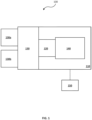
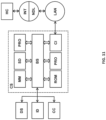
- the particle beam system 100 includes a main chamber 110, a load-lock chamber 120, a particle beam tool 140, and an equipment front end module (EFEM) 130.
- Particle beam tool 140 is located within main chamber 110.
- the exemplary particle beam system 100 may be a single or multi-beam system.
- a multi-beam system may be a parallel beam system.
- a parallel beam system may be a massive multi-beam particle system, such as a micro-electromechanical system (MEMS), including MEMS-lite systems with as many as --3000 particle beams, full-MEMS systems with as many as -18,000 particle beams. While the description and drawings are directed to a particle beam, it is appreciated that the embodiments are not used to limit the present disclosure to specific particles.
- Particles may include charged particles, such as electrons, ions, protons, etc.
- EFEM 130 includes a first loading port 130a and a second loading port 130b.
- EFEM 130 may include additional loading port(s).
- First loading port 130a and second loading port 130b may receive wafer front opening unified pods (FOUPs) that contain wafers (e.g., semiconductor wafers or wafers made of other material(s)) or samples to be inspected (wafers and samples are collectively referred to as "wafers" hereafter).
- wafers wafer front opening unified pods
- wafers e.g., semiconductor wafers or wafers made of other material(s)
- wafers samples to be inspected
- One or more robot arms (not shown) in EFEM 130 transport the wafers to load-lock chamber 120.
- signals generated by detection of secondary electrons and backscattered electrons (or other particles) are used in combination for imaging surfaces, detecting and analyzing defects, obtaining topographical information, morphological and compositional analysis, among others.
- multiple particle beams as well as multiple detectors, it may be possible to increase imaging efficiency, throughput, etc. and decrease imaging latency time, particle beam deflection range, sample scanning range, etc. It may also be beneficial to improve particle detection efficiency, such as by use of multiple particle detectors, to obtain high-quality imaging, while maintaining high throughput such as by using multiple particle beams. Detection of reflected particles corresponding to multiple parallel beams may increase decrease scanning time, increase information acquired, etc.
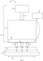
- the objective lens array assembly may be considered to be a set of objective lenses, each corresponding to a given sub-beam, which projects the plurality of sub-beams onto the sample 408.
- the objective lens array 410 comprises a plurality of objective lenses.
- "each" is use herein for a general correspondence and does not require an exact one-to-one relationship, such as between apertures and sub-beams, and items described as “each” may contain instead more than one, one, or less than one (including zero) element in relation to another element.
- the landing energy may be controlled primarily by varying the energy of the particles exiting the control lenses 422A-422C.
- the potential differences within the objective lenses 412A-412C may be preferably kept constant while the potential differences within the control lenses 422A-422C are varied, so that the electric field within the objective lenses 412A-412C remains as high as possible.
- the potentials applied to the control lenses 422A-422C may also be used to optimize the beam opening angle and demagnification.
- the control lenses 422A-422C may function to change the demagnification in view of changes in landing energy.
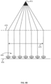
- the particle detector 570 may contain up 1,800 detector elements 560.
- the particle detector 570 may contain up to 30,000 detector elements 560.
- the particle detector 570 may be part of an objective lens, such as comprising a sample-side surface of an objective lens.
- the particle detector 570 may have areas which are not covered by detector elements 560, such as edge areas, a central beam area, etc.
- the particle detector 570 may be a BSE electron detector, a SE electron detector, etc.
- the particle detector 570 may comprise detector elements 560 which are substantially similar (e.g., as depicted) or which vary, such as based on location.
- the detector elements 560 of the particle detector 570 may vary in size, separation, orientation (e.g., along an out of plane angle) across the surface of the particle detector 570.
- the characteristics of the resonator may be altered such that they correspond, including linearly, to a quantity measured by the detector element.
- the characteristics of the resonator may be altered (e.g., by the detector) which may result in a change or alteration of a phase, wavelength, amplitude, etc. of an electromagnetic wave (e.g., light) which interacts (e.g., is incident to, travels along, etc.) with the resonator.
- the characteristics of the resonator may be measured with respect to a base characteristic, such as an input phase, a resonance wavelength, and input amplitude, etc. of the wave interacting with (e.g., incident on) the resonator.
- the detector surround 604 may instead be different material, such as a structural support, and makes up the detector surround 554.
- the beam aperture 606 may be any appropriate beam aperture, such as previously described in relation to beam aperture 556 of Figure 6A .
- the detector element 610 may have a non-negligible thickness, such as in the out of plane direction.
- the detector element 610 may be heterogeneously or homogeneously integrated circuit.
- the detector element 610 may comprise silicon CMOS devices.
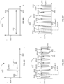
- the optical ring resonator 622 may be a ring resonator, a disk resonator (such as of a material transparent to charged particles), a whispering gallery resonator or operating in whispering gallery mode (WGM), or any other ring resonator structure.
- the optical ring resonator 622 may be symmetric (e.g., substantially round).
- the optical ring resonator 622 may have an asymmetric (e.g., radially) or otherwise not round shape in a plane view.
- the optical ring resonator 622 may be a racetrack resonator or any other appropriate shape.
- the optical ring resonator 622 may present a parallelogram in cross-section (for example, be substantially rectangular in cross-section). In one embodiment, the optical ring resonator 622 may have angled sidewalls. In one embodiment, the optical ring resonator 622 may have curved sidewalls.
- the optical ring resonator 622 may be constructed in a conductive material, such as of a metal, in a nonconductive material, such as in quartz, or in a semiconductor.
- the optical ring resonator 622 may have a bandgap (or energy bands) such that the optical ring resonator 622 is substantially transparent to optical wavelengths near the resonance wavelength.
- the optical ring resonator 622 may be comprised of multiple materials or multiple resonators, such as optically coupled double ring resonators (e.g., optical ring resonator mirrors), or any other appropriate structures.
- the output 626B may be negligible (e.g., if substantially all light is reflected), may be non-signal carrying light (e.g., if only resonance wavelengths are reflected), etc.
- the output 626B may contain one or more non-reflective termination elements.
- the waveguide 624 may be connected to multiple optical ring resonators, in addition to the optical ring resonator 622, including optical ring resonators corresponding to other detector elements than detector element 610.
- the photonic crystal 640 may be a photonic crystal resonator, such as a photonic crystal that functions as a resonator.
- the photonic crystal 640 may be photonic crystal filter, which permits transmission of some wavelengths of input light.
- the photonic crystal 640 may be a one-dimensional (or quasi-one-dimensional) photonic crystal, a two-dimensional photonic crystal, a three-dimensional photonic crystal, etc.
- the photonic crystal 640 may be a photonic crystal nanocavity.
- the photonic crystal 640 may be integrated into a waveguide, such as a photonic crystal waveguide.
- the photonic crystal 640 may be contacted by an input light source, such as a waveguide.
- Figure 7C is a plan view of a linear resonator 660 associated with detector element 650.
- the detector element 650 may be any appropriate detector element, such as the detector element 610 or 630 previously described in relation to Figure 7A and Figure 7B .
- the detector element 650 is depicted in a backside view, where the detector surface 602, detector surround 604, and beam aperture 606 are visible as projections from the detector element 650 frontside.
- the linear resonator 660 may be a resonator cavity 668.
- the linear resonator 660 comprises one or more reflector (e.g., reflectors 662A and 662B), along with the resonator cavity 668 between the reflectors 662A and 662B.
- Two reflectors 662A and 662B are depicted, but three or more reflectors may be used.
- a single resonator cavity 668 is depicted, but two or more resonator cavities, including in series, in parallel, etc., may be used.
- the reflectors 662A and 662B may be integrated reflectors, such as integrated into a waveguide or other optical material.
- the linear resonator 660 may have an input 664A, such as through the reflector 662A, and an output 664B, such as occurring through-such as through an aperture or a quasi-permeable region of-the reflector 662B.
- the linear resonator 660 may be any appropriate linear resonator.
- the linear resonator 660 may be integrated within the area of the detector element 650, or may occupy space across two or more detector elements.
- a resonance wavelength of the linear resonator 660 may be altered by a modulator of the detector element 650.
- the modulator may be any appropriate modulator, such as previously described.
- the modulator may alter physical (e.g., length), electrical (e.g., dielectric), chemical (e.g., atomic polarization), etc. characteristics of the linear resonator 660 and thereby alter one or more resonance wavelengths of the linear resonator 660.
- the modulator may alter characteristics of one or more of the reflectors 662A and 662B or of the resonator cavity 668.
- Figures 8A-8B are schematic diagrams of relationships between multiple resonators.
- Figure 8A is a graph 700 which illustrates, as a function of wavelength along the x-axis 702 and intensity along the y-axis 704, a relationship between resonance wavelengths for two resonators, which may be optical ring resonators, linear resonators, photonic crystal nanocavities, etc.
- a first resonator has resonance peaks 710A-710D, while a second resonator has resonance peaks 730A-730C, in the wavelength range depicted along the x-axis 702.
- Resonance peaks which may correspond to transmitted light from the resonators, may instead be resonance valleys, which may correspond to destructively interfered, scattered, absorbed, refracted, etc. by the resonators near the resonance wavelength.
- Each resonance peak may correspond to a resonance wavelength (e.g., resonance wavelengths 706A-706D for resonance peaks 710A-710D and resonance wavelengths 726A-726C for resonance peaks 730A-730C), which may be a central wavelength, a most intense wavelength, etc.
- the shape of the resonance peaks may vary based on the type of resonator, the type of interrogator (e.g., the type of input wavelength), the measurement device, etc.
- the shape of the resonance peaks may be Gaussian, Lorentzian, etc.
- the resonance wavelengths 706A-706D for resonance peaks 710A-710D and the resonance wavelengths 726A-726C for resonance peaks 730A-730C may be identified by curve fitting, including by curve fitting in frequency space, based on transforms (such as Fast Fourier Transforms (FFTs)), etc.
- FFTs Fast Fourier Transforms
- Resonators including optical resonators, may have multiple resonance wavelengths.
- OPD optical path length difference
- a radius of approximately 40 ⁇ m, n eff corresponding to silicon in air (e.g., 3.88), and the resonance wavelengths may correspond to approximately modes near m--630.
- the number of excited modes may depend on the bandwidth of input light, drift over time of the wavelength of the input light, measurement time, etc.
- a free spectral range (FSR) is the difference between resonant modes of the resonator, The FSR may vary based on the resonator size, resonator material, input wavelength, etc. and may be ⁇ 4 nm.
- the separation between the resonant peaks may vary based on the mode number (e.g., based on wavelength), but for large mode numbers FSR may be considered substantially constant within adjacent modes (e.g., for modes of m ⁇ 10).
- the first resonator has FSR 712, given by the difference between resonance wavelengths 706A and 706B, between the resonance wavelengths 706B and 706C, etc. which may be substantially equal over the wavelength range depicted in the graph 700.
- the second resonator has FSR 722, given by the difference between the resonance wavelengths 726A and 726C and between the resonance wavelengths 726B and 726C, etc. which, as described for the first resonator, may be substantially equal over the wavelength range depicted in the graph 700.
- the resonance peaks 710A-710D of the first resonator may have a linewidth 708.
- the resonance peaks 730A-730C may have a linewidth 728.
- the linewidth may be measured based on a curve fitting of the resonance peak or experimentally, such as as a full-width half-max (FWHM).
- the linewidth for the resonance peak may be dependent on the Q factor of the resonator, such as by the relationship given in Equation 2, below:
- Q the dimensionless quality factor
- f r is the resonance frequency
- ⁇ f the linewidth in frequency
- ⁇ r is the resonance angular frequency
- ⁇ ⁇ is the linewidth in angular frequency
- ⁇ r is the resonance wavelength
- ⁇ ⁇ is the linewidth in wavelengths.
- the linewidth of the resonance peaks is expected to be about 1.5 pm. Linewidth may be independent for the size of the resonator, but may depend upon fabrication and material quality.
- the FSR may depend on the size of a resonator.
- fewer parallel optical channels may be resolvable. For example, if the Q factor is 10 5 and the resonator radius -40 ⁇ m, the linewidth may be 14 pm and the FSR may be 3.82 nm. This may reduce the available parallel channels which can be individually resolved for readout to approximately -300 channels, or roughly 300 detector elements which may be interrogated.
- Figure 8B is a plane view of a branch 750 of an optical multiplexer.
- the branch has a set of multiple resonators 760A-760I optically connected to a waveguide 752.
- the waveguide 752 may receive input light from a direction 754 and output light to a direction 756. Alternatively or instead, the waveguide 752 may output light to the direction 754.
- the light input to the waveguide 752 may interact with one or more of the multiple resonators 760A-760I.
- the multiple resonators 760A-760I are depicted as ring resonators, but it should be understood that they may instead or additional be linear resonators, photonic crystals, etc.
- the multiple resonators 760A-760I may have individual characteristics, such as ring resonator radius, ring resonator material, individual refractive index, etc., which may lead the multiple ring resonators 760A-760I to have individual resonance wavelengths (or resonance peaks).
- the peak 810 may have a smaller linewidth than expected for the resonators, such that the resolution of the resonator resonance linewidth is a function (e.g., convolution) of substantially only the resonator Q factor.
- the peak 810 may instead be multiple peaks, such as from two or more multiplexed sources.
- Figure 8D is a graph 820 which illustrates, as a function of wavelength along the x-axis 822 and intensity along the y-axis 824, an example broadband input signal for interrogation of one or more resonators, which may be optical ring resonators, linear resonators, photonic crystal nanocavities, etc.
- An intensity 830 is produced for a range of wavelengths 832.
- the range of wavelengths 832 may correspond to one or more FSR of the one or more optical wavelengths.
- the intensity 830 may be substantially constant over the range of wavelengths, vary over the wavelengths, etc.
- Figure 8E is a graph 840 which illustrates, as a function of wavelength along the x-axis 842 and intensity along the y-axis 844, an example output signal 850 (solid line) after interrogation of one or more resonators, where the resonators scatter resonance wavelengths.
- the one or more resonators may be optical ring resonators, linear resonators, photonic crystal nanocavities, etc.
- the one or more resonators may selectively pick up optical signals corresponding to resonance peaks, thereby removing such resonance peaks from transmitted light.
- the one or more resonators may also or instead transmit the optical signals corresponding to the resonance peaks to another output waveguide, to an optical sink, etc.
- Each of the plurality of resonators may have (e.g., be tuned to) an individual resonance wavelength, where each of the resonance wavelengths may be different from all other resonance wavelengths.
- this is shown where absorption peaks 854A-854I are non-overlapping.
- the absorption peaks 854A-854I may be overlapping, but resolvable such as through peak fitting.
- the example output signal 850 may correspond to interrogation of the one or more resonators when the detector elements (to which they correspond) are not active.
- the example output signal 850 may correspond to interrogation of the one or more resonators (e.g., the multiple resonators 760A-760I of Figure 8B ) where the detector elements detect no particles or otherwise emit no output signals to the corresponding modulators.
- the absorption (where absorption may indicate only an absence of transmission or opacity at a given wavelength) peaks 854A-854I may each correspond to one of the multiple resonators 760A-760I of Figure 8B .
- An example detection signal 852 (dashed line) may correspond to interrogation of the one or more resonators when at least some of the detector elements (to which they correspond) are active.
- the example detection signal 852 may correspond to interrogation of the one or more resonators (e.g., the multiple resonators 760A-760I of Figure 8B ) where at least some of the detector elements detect particles and emit signals to the corresponding modulators, which alter resonance characteristics of some of the one or more resonators.
- the offset (e.g., in wavelength or intensity) of the absorption peaks 854A-854I in the example output signal 850 and in the example detection signal 852 may encode the output signals of the various detector elements (such as of the multiple resonators 760A-760I of Figure 8B ).
- the offset in wavelength and the offset in intensity may be related, as resonator intensity may fall in intensity as modulation is applied to alter the resonance wavelength.
- Figure 8F is a graph 860 which illustrates, as a function of wavelength along the x-axis 862 and intensity along the y-axis 864, an example output signal 870 after interrogation of one or more resonators, where the resonators emit resonance wavelengths.
- the one or more resonators may be optical ring resonators, linear resonators, photonic crystal nanocavities, etc.
- the one or more resonators may selectively pick up optical signals corresponding to resonance peaks, such as from a waveguide, and transmit the optical signals corresponding to the resonance peaks to another or the same waveguide.
- the one or more resonators may also or instead block or not transmit the optical signals which do not correspond to the resonance peaks.
- the example output signal 870 may correspond to interrogation of the one or more resonators when the detector elements (to which they correspond) are not active. That is, the example output signal 870 may correspond to interrogation of the one or more resonators (e.g., the multiple resonators 760A-760I of Figure 8B ) where the detector elements detect no particles or otherwise emit no output signals to the corresponding modulators.
- the transmission (where transmission may indicate transparency at a given wavelength) peaks 874A-874I may each correspond to one of the multiple resonators 760A-760I of Figure 8B .
- An example detection signal 872 may correspond to interrogation of the one or more resonators when at least some of the detector elements (to which they correspond) are active. That is, the example detection signal 872 may correspond to interrogation of the one or more resonators (e.g., the multiple resonators 760A-760I of Figure 8B ) where at least some of the detector elements detect particles and emit signals to the corresponding modulators, which alter resonance characteristics of some of the one or more resonators.
- the example detection signal 872 may correspond to interrogation of the one or more resonators (e.g., the multiple resonators 760A-760I of Figure 8B ) where at least some of the detector elements detect particles and emit signals to the corresponding modulators, which alter resonance characteristics of some of the one or more resonators.
- the offset (e.g., in wavelength or intensity) of the absorption peaks 874A-874I in the example output signal 870 and in the example detection signal 872 may encode the output signals of the various detector elements (such as of the multiple resonators 760A-760I of Figure 8B ).
- the offset in wavelength and the offset in intensity may be related, as resonator intensity may fall in intensity as modulation is applied to alter the resonance wavelength.
- the intensity of the transmitted signal may be limited by the strength of the input optical signal.
- the example output signal 870 or the example detection signal 872 may be detected by scanning across a wavelength range, by a detector or a source. If the source is a narrow linewidth source, such as depicted in the graph 800 of Figure 8C , the detector may detect the example output signal 870 of the example detection signal 872 based on intensity without respect to wavelength. If the source is a broadband source, such as depicted in the graph 820 of Figure 8D , the detector may detect the example output signal 870 or the example detection signal 872 by sweeping a wavelength range window (e.g., the range window 876) across a range of wavelengths as a function of time. The example output signal 870 or the example detection signal 872 may be detected in intensity and correlated to wavelength based on information about the sweeping of the optical source wavelength or detector range.
- a wavelength range window e.g., the range window 8736
- the AWG 908A contains a free space 904A, where light from the input 902 propagates, from which the light enters a set of optical fibers 940A each having a different length and therefore applying a different phase shift. The light from the optical fibers then traverses another free space 906A, where the light with different phases constructively and destructively interferes, to produce light of wavelength range at various output locations connected to optical fibers 914, 924, and 934.
- the AWG 908A may supply each branch of the optical multiplexer with a limited bandwidth of light, such as if the input 902 receives a broadband or multiple peak input optical signal.
- the multiple branches of the optical multiplexer may be interrogated by corresponding multiple input signals, and may output corresponding multiple output signals.
- the multiple output signals may be multiplexed by the AWG 908B or another appropriate element.
- the AWG 908B may operate in reverse of the AWG 908A, where the multiple output signals are received at a free space 906B, for example from optical fibers 916, 926, 936, where the multiple output signals interfere constructively and destructively and are output to multiple optical fibers 940B with different path.
- the multiple optical fibers 940B supply the light to another free space 904B where the light propagates to an output 903, which may be optically connected to one or more optical detector.
- the AWG 908A and 908B may be the same or different splitting elements.
- the detector elements 910, 920, 930 may be the same or different detector elements.
- the waveguides 912, 922, 932 may be the same or different waveguide materials.
- the waveguides 912, 922, 932 are depicted as linear waveguides, but can instead be curved waveguides, such that the detector elements 910, 920, 930 may be arranged along multiple beam paths of a particle beam apparatus, such as linearly, by close packing, etc.
- the multiple branches of the optical multiplexer may be used to interrogate up to 10 or more separate bandwidths (for example, corresponding to increments in bandwidth substantially equal to the FSR of the detector elements).
- Figure 10 is a flowchart which illustrates a method of detecting multiple particle beams. Each of these operations is described in detail below.
- the operations of method 1000 presented below are intended to be illustrative. In some embodiments, method 1000 may be accomplished with one or more additional operations not described, and/or without one or more of the operations discussed. Additionally, the order in which the operations of method 1000 are illustrated in Figure 10 and described below is not intended to be limiting.
- one or more portions of method 1000 may be implemented (e.g., by simulation, modeling, etc.) in one or more processing devices (e.g., one or more processors).
- the one or more processing devices may include one or more devices executing some or all of the operations of method 1000 in response to instructions stored electronically on an electronic storage medium.
- the one or more processing devices may include one or more devices configured through hardware, firmware, and/or software to be specifically designed for execution of one or more of the operations of method 1000, for example.
- the resonance wavelengths may be identified as corresponding to a given of the plurality of resonators.
- the resonance wavelengths may be identified as corresponding to a given of the plurality of detectors.
- the resonance wavelengths may be identified as corresponding to a given of the detected signals.
- the signals detected by the plurality of detectors are determined, based on the resonance wavelengths.
- the signals detected by the plurality of detectors may be determined based on the difference between baseline resonance wavelengths and the detected resonance wavelengths of the plurality of resonators.
- the detected signals may be encoded, by the modulators, in the difference between the baseline resonance wavelengths and the detected resonance wavelengths and may be decoded.
- the signals detected by the plurality of detectors may be determined based on a resonance wavelength shift, a resonance intensity difference, etc.
- the signals detected by the plurality of detectors may be determined in any appropriate manner, such as those previously described.
- the signals detected by the plurality of detectors may be determined and used to create an image, such as of a scanning electron micrograph.
- the signals detected by the plurality of detectors may correspond to pixels of the image.
- the signals detected by the plurality of detectors may correspond to pixel values of the pixels of the image.
- the signals detected by the plurality of detectors may be acquired repeatedly, and such repeated signals may correspond to additional pixels of the image.
- the signals detected by the plurality of detectors may be used to construct, reconstruct, etc. information about a sample, where the signals detected by the plurality of detectors may be produced by interaction of particles with the sample.
- Computer system CS may be coupled via bus BS to a display DS, such as a cathode ray tube (CRT) or flat panel or touch panel display for displaying information to a computer user.
- a display DS such as a cathode ray tube (CRT) or flat panel or touch panel display for displaying information to a computer user.
- An input device ID is coupled to bus BS for communicating information and command selections to processor PRO.
- cursor control CC is Another type of user input device, such as a mouse, a trackball, or cursor direction keys for communicating direction information and command selections to processor PRO and for controlling cursor movement on display DS.
- This input device typically has two degrees of freedom in two axes, a first axis (e.g., x) and a second axis (e.g., y), that allows the device to specify positions in a plane.
- a touch panel (screen) display may also be used as an input device.
- Non-volatile media include, for example, optical or magnetic disks, such as storage device SD.
- Volatile media include dynamic memory, such as main memory MM.
- Transmission media include coaxial cables, copper wire and fiber optics, including the wires that comprise bus BS. Transmission media can also take the form of acoustic or light waves, such as those generated during radio frequency (RF) and infrared (IR) data communications.
- RF radio frequency
- IR infrared
- Computer system CS may also include a communication interface CI coupled to bus BS.
- Communication interface CI provides a two-way data communication coupling to a network link NDL that is connected to a local network LAN.
- communication interface CI may be an integrated services digital network (ISDN) card or a modem to provide a data communication connection to a corresponding type of telephone line.
- ISDN integrated services digital network
- communication interface CI may be a local area network (LAN) card to provide a data communication connection to a compatible LAN.
- LAN local area network
- Wireless links may also be implemented.
- communication interface CI sends and receives electrical, electromagnetic, or optical signals that carry digital data streams representing various types of information.
Landscapes
- Chemical & Material Sciences (AREA)
- Analytical Chemistry (AREA)
- Analysing Materials By The Use Of Radiation (AREA)
Priority Applications (1)
| Application Number | Priority Date | Filing Date | Title |
|---|---|---|---|
| EP22217433.6A EP4394841A1 (de) | 2022-12-31 | 2022-12-31 | Multiplex-ausleseverfahren für parallele elektronendetektoren |
Applications Claiming Priority (1)
| Application Number | Priority Date | Filing Date | Title |
|---|---|---|---|
| EP22217433.6A EP4394841A1 (de) | 2022-12-31 | 2022-12-31 | Multiplex-ausleseverfahren für parallele elektronendetektoren |
Publications (1)
| Publication Number | Publication Date |
|---|---|
| EP4394841A1 true EP4394841A1 (de) | 2024-07-03 |
Family
ID=84785244
Family Applications (1)
| Application Number | Title | Priority Date | Filing Date |
|---|---|---|---|
| EP22217433.6A Withdrawn EP4394841A1 (de) | 2022-12-31 | 2022-12-31 | Multiplex-ausleseverfahren für parallele elektronendetektoren |
Country Status (1)
| Country | Link |
|---|---|
| EP (1) | EP4394841A1 (de) |
Cited By (1)
| Publication number | Priority date | Publication date | Assignee | Title |
|---|---|---|---|---|
| EP4678090A1 (de) * | 2024-07-10 | 2026-01-14 | Imec VZW | Sensorvorrichtung, photoakustische bildgebungsvorrichtung und verfahren zum auslesen einer erfassten messgrösse |
Citations (3)
| Publication number | Priority date | Publication date | Assignee | Title |
|---|---|---|---|---|
| WO2010051848A1 (en) | 2008-11-07 | 2010-05-14 | H. Folke Sandelin Ab | Methods and system for manufacturing lead battery plates |
| US7764850B2 (en) * | 2008-01-25 | 2010-07-27 | Hewlett-Packard Development Company, L.P. | Optical modulator including electrically controlled ring resonator |
| US10284824B2 (en) * | 2017-01-20 | 2019-05-07 | Caeleste Cvba | Opto-electronic stacked sensor |
-
2022
- 2022-12-31 EP EP22217433.6A patent/EP4394841A1/de not_active Withdrawn
Patent Citations (3)
| Publication number | Priority date | Publication date | Assignee | Title |
|---|---|---|---|---|
| US7764850B2 (en) * | 2008-01-25 | 2010-07-27 | Hewlett-Packard Development Company, L.P. | Optical modulator including electrically controlled ring resonator |
| WO2010051848A1 (en) | 2008-11-07 | 2010-05-14 | H. Folke Sandelin Ab | Methods and system for manufacturing lead battery plates |
| US10284824B2 (en) * | 2017-01-20 | 2019-05-07 | Caeleste Cvba | Opto-electronic stacked sensor |
Non-Patent Citations (3)
| Title |
|---|
| "SEMICONDUCTOR CHARGED PARTICLE DETECTOR FOR MICROSCOPY", vol. 685, no. 82, 1 May 2021 (2021-05-01), XP007149412, ISSN: 0374-4353, Retrieved from the Internet <URL:https://www.researchdisclosure.com/database/RD685082> * |
| LASSE JUHANA KAUPPINEN: "COMPACT INTEGRATED OPTICAL DEVICES FOR OPTICAL SENSOR AND SWITCHING APPLICATIONS", PHD THESIS, 1 January 2010 (2010-01-01), pages 1 - 126, XP055538648, Retrieved from the Internet <URL:http://dx.doi.org/10.3990/1.9789036530880> [retrieved on 20190107] * |
| SINATKAS GEORGIOS ET AL: "Electro-optic modulation in integrated photonics", JOURNAL OF APPLIED PHYSICS, AMERICAN INSTITUTE OF PHYSICS, 2 HUNTINGTON QUADRANGLE, MELVILLE, NY 11747, vol. 130, no. 1, 2 July 2021 (2021-07-02), XP012257868, ISSN: 0021-8979, [retrieved on 20210702], DOI: 10.1063/5.0048712 * |
Cited By (1)
| Publication number | Priority date | Publication date | Assignee | Title |
|---|---|---|---|---|
| EP4678090A1 (de) * | 2024-07-10 | 2026-01-14 | Imec VZW | Sensorvorrichtung, photoakustische bildgebungsvorrichtung und verfahren zum auslesen einer erfassten messgrösse |
Similar Documents
| Publication | Publication Date | Title |
|---|---|---|
| US7075072B2 (en) | Detecting apparatus and device manufacturing method | |
| US11942302B2 (en) | Pulsed charged-particle beam system | |
| EP4123579A1 (de) | Datenverarbeitungsvorrichtung und -verfahren, system und verfahren zur bewertung geladener teilchen | |
| US20250253123A1 (en) | Charged particle-optical apparatus | |
| CN110574139A (zh) | 使用多个带电粒子束的设备 | |
| TWI859536B (zh) | 偵測樣本影像中之缺陷的電腦可實施方法及資料處理裝置 | |
| EP4394841A1 (de) | Multiplex-ausleseverfahren für parallele elektronendetektoren | |
| US20240369356A1 (en) | Inspection apparatus and method | |
| EP4092614A1 (de) | Datenverarbeitungsvorrichtung und -verfahren, system und verfahren zur bewertung geladener teilchen | |
| JP2023516114A (ja) | マルチビーム検査システム用のビーム・アレイ・ジオメトリ最適化装置 | |
| US12165836B2 (en) | Systems and methods of profiling charged-particle beams | |
| CN117769753A (zh) | 带电粒子光学设备 | |
| US20140061465A1 (en) | Electron beam detector, electron beam processing apparatus, and method of manufacturing electron beam detector | |
| Maidment | Development of an integrated multispectral LIDAR in silicon photonics | |
| EP4593056A2 (de) | Element für optische strahlung | |
| US20250087444A1 (en) | Data processing device and method, charged particle assessment system and method | |
| CN115803843B (zh) | 用于透射电子显微镜阴极发光的装置 | |
| EP4421843A1 (de) | Optische vorrichtung für geladene teilchen | |
| EP4411783A1 (de) | Holographie auf basis niederenergetischer elektronenmikroskopie | |
| TW202544860A (zh) | 帶電粒子光學裝置及處理樣品之方法 | |
| KR20240134220A (ko) | 하전 입자선 장치의 조정 방법 및 하전 입자선 장치 | |
| KR20250037408A (ko) | 현미경용 하전 입자 검출기 | |
| TW202541085A (zh) | 藉由動態補償進行影像漣波校正 |
Legal Events
| Date | Code | Title | Description |
|---|---|---|---|
| PUAI | Public reference made under article 153(3) epc to a published international application that has entered the european phase |
Free format text: ORIGINAL CODE: 0009012 |
|
| STAA | Information on the status of an ep patent application or granted ep patent |
Free format text: STATUS: THE APPLICATION HAS BEEN PUBLISHED |
|
| AK | Designated contracting states |
Kind code of ref document: A1 Designated state(s): AL AT BE BG CH CY CZ DE DK EE ES FI FR GB GR HR HU IE IS IT LI LT LU LV MC ME MK MT NL NO PL PT RO RS SE SI SK SM TR |
|
| STAA | Information on the status of an ep patent application or granted ep patent |
Free format text: STATUS: THE APPLICATION IS DEEMED TO BE WITHDRAWN |
|
| 18D | Application deemed to be withdrawn |
Effective date: 20250104 |