EP4394750A1 - Display apparatus and driving method thereof - Google Patents
Display apparatus and driving method thereof Download PDFInfo
- Publication number
- EP4394750A1 EP4394750A1 EP23208662.9A EP23208662A EP4394750A1 EP 4394750 A1 EP4394750 A1 EP 4394750A1 EP 23208662 A EP23208662 A EP 23208662A EP 4394750 A1 EP4394750 A1 EP 4394750A1
- Authority
- EP
- European Patent Office
- Prior art keywords
- resolution
- gate
- image
- per
- display panel
- Prior art date
- Legal status (The legal status is an assumption and is not a legal conclusion. Google has not performed a legal analysis and makes no representation as to the accuracy of the status listed.)
- Pending
Links
Images








Classifications
-
- G—PHYSICS
- G09—EDUCATION; CRYPTOGRAPHY; DISPLAY; ADVERTISING; SEALS
- G09G—ARRANGEMENTS OR CIRCUITS FOR CONTROL OF INDICATING DEVICES USING STATIC MEANS TO PRESENT VARIABLE INFORMATION
- G09G3/00—Control arrangements or circuits, of interest only in connection with visual indicators other than cathode-ray tubes
- G09G3/20—Control arrangements or circuits, of interest only in connection with visual indicators other than cathode-ray tubes for presentation of an assembly of a number of characters, e.g. a page, by composing the assembly by combination of individual elements arranged in a matrix no fixed position being assigned to or needed to be assigned to the individual characters or partial characters
- G09G3/22—Control arrangements or circuits, of interest only in connection with visual indicators other than cathode-ray tubes for presentation of an assembly of a number of characters, e.g. a page, by composing the assembly by combination of individual elements arranged in a matrix no fixed position being assigned to or needed to be assigned to the individual characters or partial characters using controlled light sources
- G09G3/30—Control arrangements or circuits, of interest only in connection with visual indicators other than cathode-ray tubes for presentation of an assembly of a number of characters, e.g. a page, by composing the assembly by combination of individual elements arranged in a matrix no fixed position being assigned to or needed to be assigned to the individual characters or partial characters using controlled light sources using electroluminescent panels
- G09G3/32—Control arrangements or circuits, of interest only in connection with visual indicators other than cathode-ray tubes for presentation of an assembly of a number of characters, e.g. a page, by composing the assembly by combination of individual elements arranged in a matrix no fixed position being assigned to or needed to be assigned to the individual characters or partial characters using controlled light sources using electroluminescent panels semiconductive, e.g. using light-emitting diodes [LED]
- G09G3/3208—Control arrangements or circuits, of interest only in connection with visual indicators other than cathode-ray tubes for presentation of an assembly of a number of characters, e.g. a page, by composing the assembly by combination of individual elements arranged in a matrix no fixed position being assigned to or needed to be assigned to the individual characters or partial characters using controlled light sources using electroluminescent panels semiconductive, e.g. using light-emitting diodes [LED] organic, e.g. using organic light-emitting diodes [OLED]
- G09G3/3266—Details of drivers for scan electrodes
-
- G—PHYSICS
- G09—EDUCATION; CRYPTOGRAPHY; DISPLAY; ADVERTISING; SEALS
- G09G—ARRANGEMENTS OR CIRCUITS FOR CONTROL OF INDICATING DEVICES USING STATIC MEANS TO PRESENT VARIABLE INFORMATION
- G09G3/00—Control arrangements or circuits, of interest only in connection with visual indicators other than cathode-ray tubes
- G09G3/20—Control arrangements or circuits, of interest only in connection with visual indicators other than cathode-ray tubes for presentation of an assembly of a number of characters, e.g. a page, by composing the assembly by combination of individual elements arranged in a matrix no fixed position being assigned to or needed to be assigned to the individual characters or partial characters
- G09G3/22—Control arrangements or circuits, of interest only in connection with visual indicators other than cathode-ray tubes for presentation of an assembly of a number of characters, e.g. a page, by composing the assembly by combination of individual elements arranged in a matrix no fixed position being assigned to or needed to be assigned to the individual characters or partial characters using controlled light sources
- G09G3/30—Control arrangements or circuits, of interest only in connection with visual indicators other than cathode-ray tubes for presentation of an assembly of a number of characters, e.g. a page, by composing the assembly by combination of individual elements arranged in a matrix no fixed position being assigned to or needed to be assigned to the individual characters or partial characters using controlled light sources using electroluminescent panels
-
- G—PHYSICS
- G09—EDUCATION; CRYPTOGRAPHY; DISPLAY; ADVERTISING; SEALS
- G09G—ARRANGEMENTS OR CIRCUITS FOR CONTROL OF INDICATING DEVICES USING STATIC MEANS TO PRESENT VARIABLE INFORMATION
- G09G3/00—Control arrangements or circuits, of interest only in connection with visual indicators other than cathode-ray tubes
- G09G3/20—Control arrangements or circuits, of interest only in connection with visual indicators other than cathode-ray tubes for presentation of an assembly of a number of characters, e.g. a page, by composing the assembly by combination of individual elements arranged in a matrix no fixed position being assigned to or needed to be assigned to the individual characters or partial characters
- G09G3/34—Control arrangements or circuits, of interest only in connection with visual indicators other than cathode-ray tubes for presentation of an assembly of a number of characters, e.g. a page, by composing the assembly by combination of individual elements arranged in a matrix no fixed position being assigned to or needed to be assigned to the individual characters or partial characters by control of light from an independent source
- G09G3/36—Control arrangements or circuits, of interest only in connection with visual indicators other than cathode-ray tubes for presentation of an assembly of a number of characters, e.g. a page, by composing the assembly by combination of individual elements arranged in a matrix no fixed position being assigned to or needed to be assigned to the individual characters or partial characters by control of light from an independent source using liquid crystals
- G09G3/3611—Control of matrices with row and column drivers
- G09G3/3648—Control of matrices with row and column drivers using an active matrix
-
- G—PHYSICS
- G09—EDUCATION; CRYPTOGRAPHY; DISPLAY; ADVERTISING; SEALS
- G09G—ARRANGEMENTS OR CIRCUITS FOR CONTROL OF INDICATING DEVICES USING STATIC MEANS TO PRESENT VARIABLE INFORMATION
- G09G3/00—Control arrangements or circuits, of interest only in connection with visual indicators other than cathode-ray tubes
- G09G3/20—Control arrangements or circuits, of interest only in connection with visual indicators other than cathode-ray tubes for presentation of an assembly of a number of characters, e.g. a page, by composing the assembly by combination of individual elements arranged in a matrix no fixed position being assigned to or needed to be assigned to the individual characters or partial characters
- G09G3/22—Control arrangements or circuits, of interest only in connection with visual indicators other than cathode-ray tubes for presentation of an assembly of a number of characters, e.g. a page, by composing the assembly by combination of individual elements arranged in a matrix no fixed position being assigned to or needed to be assigned to the individual characters or partial characters using controlled light sources
-
- G—PHYSICS
- G09—EDUCATION; CRYPTOGRAPHY; DISPLAY; ADVERTISING; SEALS
- G09G—ARRANGEMENTS OR CIRCUITS FOR CONTROL OF INDICATING DEVICES USING STATIC MEANS TO PRESENT VARIABLE INFORMATION
- G09G3/00—Control arrangements or circuits, of interest only in connection with visual indicators other than cathode-ray tubes
- G09G3/20—Control arrangements or circuits, of interest only in connection with visual indicators other than cathode-ray tubes for presentation of an assembly of a number of characters, e.g. a page, by composing the assembly by combination of individual elements arranged in a matrix no fixed position being assigned to or needed to be assigned to the individual characters or partial characters
- G09G3/34—Control arrangements or circuits, of interest only in connection with visual indicators other than cathode-ray tubes for presentation of an assembly of a number of characters, e.g. a page, by composing the assembly by combination of individual elements arranged in a matrix no fixed position being assigned to or needed to be assigned to the individual characters or partial characters by control of light from an independent source
- G09G3/36—Control arrangements or circuits, of interest only in connection with visual indicators other than cathode-ray tubes for presentation of an assembly of a number of characters, e.g. a page, by composing the assembly by combination of individual elements arranged in a matrix no fixed position being assigned to or needed to be assigned to the individual characters or partial characters by control of light from an independent source using liquid crystals
- G09G3/3611—Control of matrices with row and column drivers
-
- G—PHYSICS
- G09—EDUCATION; CRYPTOGRAPHY; DISPLAY; ADVERTISING; SEALS
- G09G—ARRANGEMENTS OR CIRCUITS FOR CONTROL OF INDICATING DEVICES USING STATIC MEANS TO PRESENT VARIABLE INFORMATION
- G09G3/00—Control arrangements or circuits, of interest only in connection with visual indicators other than cathode-ray tubes
- G09G3/20—Control arrangements or circuits, of interest only in connection with visual indicators other than cathode-ray tubes for presentation of an assembly of a number of characters, e.g. a page, by composing the assembly by combination of individual elements arranged in a matrix no fixed position being assigned to or needed to be assigned to the individual characters or partial characters
- G09G3/34—Control arrangements or circuits, of interest only in connection with visual indicators other than cathode-ray tubes for presentation of an assembly of a number of characters, e.g. a page, by composing the assembly by combination of individual elements arranged in a matrix no fixed position being assigned to or needed to be assigned to the individual characters or partial characters by control of light from an independent source
- G09G3/36—Control arrangements or circuits, of interest only in connection with visual indicators other than cathode-ray tubes for presentation of an assembly of a number of characters, e.g. a page, by composing the assembly by combination of individual elements arranged in a matrix no fixed position being assigned to or needed to be assigned to the individual characters or partial characters by control of light from an independent source using liquid crystals
- G09G3/3611—Control of matrices with row and column drivers
- G09G3/3674—Details of drivers for scan electrodes
-
- G—PHYSICS
- G09—EDUCATION; CRYPTOGRAPHY; DISPLAY; ADVERTISING; SEALS
- G09G—ARRANGEMENTS OR CIRCUITS FOR CONTROL OF INDICATING DEVICES USING STATIC MEANS TO PRESENT VARIABLE INFORMATION
- G09G2310/00—Command of the display device
- G09G2310/02—Addressing, scanning or driving the display screen or processing steps related thereto
- G09G2310/0202—Addressing of scan or signal lines
-
- G—PHYSICS
- G09—EDUCATION; CRYPTOGRAPHY; DISPLAY; ADVERTISING; SEALS
- G09G—ARRANGEMENTS OR CIRCUITS FOR CONTROL OF INDICATING DEVICES USING STATIC MEANS TO PRESENT VARIABLE INFORMATION
- G09G2310/00—Command of the display device
- G09G2310/02—Addressing, scanning or driving the display screen or processing steps related thereto
- G09G2310/0243—Details of the generation of driving signals
-
- G—PHYSICS
- G09—EDUCATION; CRYPTOGRAPHY; DISPLAY; ADVERTISING; SEALS
- G09G—ARRANGEMENTS OR CIRCUITS FOR CONTROL OF INDICATING DEVICES USING STATIC MEANS TO PRESENT VARIABLE INFORMATION
- G09G2310/00—Command of the display device
- G09G2310/02—Addressing, scanning or driving the display screen or processing steps related thereto
- G09G2310/0264—Details of driving circuits
-
- G—PHYSICS
- G09—EDUCATION; CRYPTOGRAPHY; DISPLAY; ADVERTISING; SEALS
- G09G—ARRANGEMENTS OR CIRCUITS FOR CONTROL OF INDICATING DEVICES USING STATIC MEANS TO PRESENT VARIABLE INFORMATION
- G09G2310/00—Command of the display device
- G09G2310/02—Addressing, scanning or driving the display screen or processing steps related thereto
- G09G2310/0264—Details of driving circuits
- G09G2310/0267—Details of drivers for scan electrodes, other than drivers for liquid crystal, plasma or OLED displays
-
- G—PHYSICS
- G09—EDUCATION; CRYPTOGRAPHY; DISPLAY; ADVERTISING; SEALS
- G09G—ARRANGEMENTS OR CIRCUITS FOR CONTROL OF INDICATING DEVICES USING STATIC MEANS TO PRESENT VARIABLE INFORMATION
- G09G2310/00—Command of the display device
- G09G2310/08—Details of timing specific for flat panels, other than clock recovery
-
- G—PHYSICS
- G09—EDUCATION; CRYPTOGRAPHY; DISPLAY; ADVERTISING; SEALS
- G09G—ARRANGEMENTS OR CIRCUITS FOR CONTROL OF INDICATING DEVICES USING STATIC MEANS TO PRESENT VARIABLE INFORMATION
- G09G2340/00—Aspects of display data processing
- G09G2340/04—Changes in size, position or resolution of an image
-
- G—PHYSICS
- G09—EDUCATION; CRYPTOGRAPHY; DISPLAY; ADVERTISING; SEALS
- G09G—ARRANGEMENTS OR CIRCUITS FOR CONTROL OF INDICATING DEVICES USING STATIC MEANS TO PRESENT VARIABLE INFORMATION
- G09G2340/00—Aspects of display data processing
- G09G2340/04—Changes in size, position or resolution of an image
- G09G2340/0407—Resolution change, inclusive of the use of different resolutions for different screen areas
-
- G—PHYSICS
- G09—EDUCATION; CRYPTOGRAPHY; DISPLAY; ADVERTISING; SEALS
- G09G—ARRANGEMENTS OR CIRCUITS FOR CONTROL OF INDICATING DEVICES USING STATIC MEANS TO PRESENT VARIABLE INFORMATION
- G09G2340/00—Aspects of display data processing
- G09G2340/04—Changes in size, position or resolution of an image
- G09G2340/0407—Resolution change, inclusive of the use of different resolutions for different screen areas
- G09G2340/0414—Vertical resolution change
-
- G—PHYSICS
- G09—EDUCATION; CRYPTOGRAPHY; DISPLAY; ADVERTISING; SEALS
- G09G—ARRANGEMENTS OR CIRCUITS FOR CONTROL OF INDICATING DEVICES USING STATIC MEANS TO PRESENT VARIABLE INFORMATION
- G09G2340/00—Aspects of display data processing
- G09G2340/04—Changes in size, position or resolution of an image
- G09G2340/0407—Resolution change, inclusive of the use of different resolutions for different screen areas
- G09G2340/0421—Horizontal resolution change
-
- G—PHYSICS
- G09—EDUCATION; CRYPTOGRAPHY; DISPLAY; ADVERTISING; SEALS
- G09G—ARRANGEMENTS OR CIRCUITS FOR CONTROL OF INDICATING DEVICES USING STATIC MEANS TO PRESENT VARIABLE INFORMATION
- G09G2360/00—Aspects of the architecture of display systems
- G09G2360/02—Graphics controller able to handle multiple formats, e.g. input or output formats
-
- G—PHYSICS
- G09—EDUCATION; CRYPTOGRAPHY; DISPLAY; ADVERTISING; SEALS
- G09G—ARRANGEMENTS OR CIRCUITS FOR CONTROL OF INDICATING DEVICES USING STATIC MEANS TO PRESENT VARIABLE INFORMATION
- G09G3/00—Control arrangements or circuits, of interest only in connection with visual indicators other than cathode-ray tubes
- G09G3/20—Control arrangements or circuits, of interest only in connection with visual indicators other than cathode-ray tubes for presentation of an assembly of a number of characters, e.g. a page, by composing the assembly by combination of individual elements arranged in a matrix no fixed position being assigned to or needed to be assigned to the individual characters or partial characters
Definitions
- the timing controller may control the gate driver so that a position of a portion where the gate signals are applied one by one per one gate line and a position of a portion, where the gate signals are applied one by one per at least two gate lines, are alternated.
- a portion where the gate signals are applied one by one per one gate line and a portion, where the gate signals are applied one by one per at least two gate lines, may be three gate lines vertically adjacent to one another in the display panel.
- a portion where the gate signals are applied one by one per one gate line and a portion, where the gate signals are applied one by one per at least two gate lines, may be provided.
- a display apparatus may be applied to televisions (TVs), video players, personal computers (PCs), home theaters, electronic devices for vehicles, and smartphones, but is not limited thereto.
- the display apparatus according to the present disclosure may be implemented as a light emitting display apparatus, a quantum dot display (QDD) apparatus, or a liquid crystal display (LCD) apparatus.
- QDD quantum dot display
- LCD liquid crystal display
- a light emitting display apparatus self-emitting light on the basis of an inorganic light emitting diode or an organic light emitting diode will be described for example.
- a light emitting display apparatus may be implemented based on an inorganic light emitting diode, or may be implemented based on an organic light emitting diode.
- an example will be described where a light emitting display apparatus is implemented based on an organic light emitting diode.
- FIG. 1 is a block diagram schematically illustrating a display apparatus
- FIG. 2 is a block diagram schematically illustrating a subpixel illustrated in FIG. 1 .
- the light emitting display apparatus may include a video supply unit 110, a timing controller 120, a gate driver 130, a data driver 140, a display panel 150, and a power supply 180.
- the video supply unit 110 (a set or a host system) may output a video data signal supplied from the outside (ie external to the display device) or a video data signal and various driving signals stored in an internal memory thereof.
- the video supply unit 110 may supply a data signal and the various driving signals to the timing controller 120.
- the timing controller 120 may output a gate timing control signal GDC for controlling an operation timing of the gate driver 130, a data timing control signal DDC for controlling an operation timing of the data driver 140, and various synchronization signals.
- the timing controller 120 may provide the data driver 140 with the data timing control signal DDC and a data signal DATA supplied from the video supply unit 110.
- the timing controller 120 may be implemented as an integrated circuit (IC) type and may be mounted on a printed circuit board (PCB), but is not limited thereto.
- the power supply 180 may generate a high voltage and a low voltage on the basis of an external input voltage supplied from the outside and may respectively output the high voltage and the low voltage through a high voltage line EVDD and a low voltage line EVSS.
- the power supply unit 180 may generate and output a voltage (for example, a gate voltage including a gate high voltage and a gate low voltage) needed for driving of the gate driver 130 or a voltage (for example, a drain voltage including a drain voltage and a half drain voltage) needed for driving of the data driver 140, in addition to the high voltage and the low voltage.
- the display panel 150 may display an image on the basis of a driving signal, including the gate signal and a data voltage, and a driving voltage including a high level voltage and a low level voltage. Subpixels of the display panel 150 may self-emit light.
- the display panel 150 may be manufactured based on a substrate, having stiffness or flexibility, such as glass, silicon, or polyimide. Also, a pixel emitting light may include red, green, and blue subpixels, or may include red, green, blue, and white subpixels.
- one subpixel SP may be connected with a first data line DL1, a first gate line GL1, the high voltage line EVDD, and the low voltage line EVSS and may include a pixel circuit including a switching transistor, a driving transistor, a capacitor, and an organic light emitting diode.
- the subpixel SP used in the light emitting display apparatus may self-emit light, and thus, may be complicated in configuration of a circuit.
- the subpixel SP may include an organic light emitting diode emitting light and a compensation circuit which compensates for a degradation in a driving transistor which supplies a driving current needed for driving of the organic light emitting diode. Accordingly, the subpixel SP is simply illustrated in a block shape.
- each of the timing controller 120, the gate driver 130, and the data driver 140 has been described as an individual element. However, based on an implementation type of a light emitting display apparatus, one or more of the timing controller 120, the gate driver 130, and the data driver 140 may be integrated into one IC.
- the gate driver 130 of the GIP type may include a shift register 131 and a level shifter 135.
- the level shifter 135 may generate clock signals Clks and a start signal Vst, based on signals and voltages respectively output from the timing controller 120 and the power supply 180.
- the shift register 131 may operate based on the clock signals Clks and the start signal Vst output from the level shifter 135 and may output gate signals Gout[1] to Gout[m].
- the level shifter 135 may be independently provided as an IC type unlike the shift register 131, or may be included in the power supply 180. However, this may be merely an example, and the present disclosure is not limited thereto.
- FIGs. 6 to 8 are diagrams for describing a function of a display apparatus according to an example of the present disclosure.
- the display apparatus may display an image, which has various resolutions and is input from the outside, on the display panel 150.
- the display panel 150 may be implemented to display an UHD image.
- the display apparatus may selectively output one image source of image sources respectively having a first resolution AHD, a second resolution BHD, and a third resolution CHD.
- the display apparatus may include a selector SEL which selects and outputs one image source from among the image sources respectively having the first resolution AHD, the second resolution BHD, and the third resolution CHD, but in a case where an image is selectively input, the selector SEL may be omitted or may be included in an image source.
- the display apparatus may include a mode change unit DLG for changing a driving condition so as to implement an image having a specific resolution on the display panel 150.
- the mode change unit DLG may be included the timing controller 120 (ASIC) for controlling the display panel 150 and a memory DDR.
- the mode change unit DLG may change a generating condition of a mode change signal, based on whether a resolution of an image input from the outside is the first resolution AHD, the second resolution BHD, or the third resolution CHD.
- the first resolution AHD is quad high definition (QHD) (2560 * 1440)
- the second resolution BHD is full high definition (FHD) (1920 * 1080)
- the third resolution CHD is ultra-high definition; (UHD) (3840 * 2160).
- the mode change unit DLG may be included in the timing controller 120.
- the mode change unit DLG may be included in the image supply unit 110.
- the mode change unit DLG may be included in the timing controller 120, but may be implemented as a type where the mode change signal applied from the outside is intactly output (Output as is, without any changes) to the inside or the outside.
- the mode change unit DLG may supply the mode change signal through a signal line DLGS connected with an output change circuit unit 132.
- An example is illustrated where the output change circuit unit 132 is included in the shift register 131, but this may be included in the level shifter 135.
- the mode change unit DLG may not output a mode change signal DLG:OFF.
- the mode change unit DLG may output a first mode change signal DLG1 :ON.
- the mode change unit DLG may output a second mode change signal DLG2:ON.
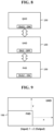
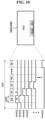
- FIGs. 9 and 10 are diagrams for describing a method of implementing an FHD image on a UHD display panel 150, according to an example of the present disclosure.
- an FHD image may be lower in resolution than an UHD image. Therefore, in order to display the FHD image on the UHD display panel 150, when a horizontal resolution "x" and a vertical resolution "y" should be extended, it may be required to change a ratio of an input to an output to 1:2.
- the timing controller 120 may extend the horizontal resolution. Also, in order to extend the vertical resolution by twice compared to a previous resolution, the timing controller 120 may control the output change circuit unit 132, based on the mode change unit DLG. This may be referred to as a gate line doubling method using a device provided outside the timing controller, so as to extend the vertical resolution.
- the mode change unit DLG may output the second mode change signal DLG2:ON.
- the shift register 131 may sequentially divide and output gate signals Gout[1] to Gout[m] which are to be supplied to the display panel 150 and may output one gate signal per two gate lines.
- two gate lines vertically adjacent to each other may receive one gate signal which is identically generated, and thus, a vertical resolution may be extended by twice compared to a previous resolution.
- subpixels connected with the first gate line and the second gate line may be simultaneously supplied with the same data voltage D1 during 1HT (horizontal time), and thus, a horizontal resolution may be extended by twice compared to a previous resolution.
- gate signals may be sequentially output up to "Gout[m].
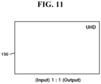
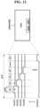
- FIGs. 11 and 12 are diagrams for describing a method of implementing an UHD image on an UHD display panel 150, according to an example of the present disclosure.
- an UHD image may be intactly displayed on the UHD display panel 150, and thus, a ratio of an input to an output may be 1:1 and it may not be required to change a resolution of an image.
- the timing controller 120 may perform only necessary image processing and may intactly output the UHD image. Also, the timing controller 120 may not use the mode change unit DLG, and thus, the output change circuit unit 132 may be in a state where an operation is not performed.
- the shift register 131 may sequentially divide and output gate signals Gout[1] to Gout[m] which are to be supplied to the display panel 150 and may output one gate signal per two gate lines.
- subpixels connected with the first gate line may be simultaneously supplied with one data voltage D1 during 1HT.
- gate signals may be sequentially output up to "Gout[m]”.
- FIGs. 13 to 16 are diagrams for describing a method of implementing a QHD image on an UHD display panel 150, according to an example of the present disclosure.
- a frame may be divided into an odd frame and an even frame, and two gate lines vertically adjacent to each other may receive one gate signal which is identically generated and then may receive gate signals which are divided and generated, whereby a vertical resolution may be extended by 1.5 times compared to a previous resolution.
- subpixels connected with the first gate line and the second gate line may be simultaneously supplied with the same data voltage D1 during 1HT (horizontal time), and thus, a horizontal resolution may be extended by twice compared to a previous resolution.
- the subpixels connected with the first gate line and the second gate line may be simultaneously supplied with different data voltage D1 and D2 at different times during 1HT (horizontal time), and thus, a horizontal resolution may be maintained by once like previous resolution.
- FIGs. 17 to 20 are diagrams for describing a resolution resizing method for displaying a QHD image on an UHD display panel, according to an example of the present disclosure.
- a horizontal resolution may be extended, a vertical resolution may be reduced, an image may be displayed, and doubling of a gate line may be performed.
- an extension of the horizontal resolution and a reduction in the vertical resolution may be performed by the timing controller or the image supply unit, and doubling of a gate line may be performed by the gate driver.
- the timing controller may control outputs of data signals and gate signals in the form of expressing an image corresponding to 3840 * 1080.
- output patterns of gate signals output from the gate driver may be changed based on the gate line doubling method, and thus, an image displayed on the display panel may finally have a resolution (3840 * 2160) corresponding to the UHD image.
- images 1 and 2 of first and second lines may be configured to be displayed as the image 1 of the first line
- images 3 and 4 of third and fourth lines may be configured to be displayed as the images 2 and 3 of the second and third lines.
- images 1 and 2 of first and second lines may be configured to be intactly displayed as the images 1 and 2 of the first and second lines
- images 3 and 4 of third and fourth lines may be configured to be displayed as the image 3 of the third line.
- Such a method may be implemented as an asymmetrical resolution implementation method which allocates images of four lines as images of three lines and alternately performs the allocation to reduce a vertical resolution to 4:3, thereby minimizing (minimizing a reduction in image quality) the loss of an image in a process of changing the QHD image to the UHD image.
- FIGs. 21 and 22 are diagrams illustrating some of elements of an apparatus according to an example of the present disclosure. A function and an operation of the apparatus illustrated in FIGs. 21 and 22 are as described above, and thus, elements performing functions and operations and an apparatus including the elements will be mainly described below.
- a display apparatus may include an input processor INP, a resolution resizer, and a mode change unit DLG, so as to easily implement an image input at various frequencies and resolutions and minimize a degradation in image quality.
- the resolution resizer may extend or reduce a vertical resolution and a horizontal resolution, based on a horizontal scaler and a vertical scaler.
- a horizontal resolution extension unit HOREX and a vertical resolution reduction unit VERRD included in the resolution resizer are illustrated and described.
- the resolution resizer may be included in the timing controller 120, or may be included in the image supply unit 110 as in FIG. 22 .
Landscapes
- Engineering & Computer Science (AREA)
- Physics & Mathematics (AREA)
- Computer Hardware Design (AREA)
- General Physics & Mathematics (AREA)
- Theoretical Computer Science (AREA)
- Chemical & Material Sciences (AREA)
- Crystallography & Structural Chemistry (AREA)
- Control Of Indicators Other Than Cathode Ray Tubes (AREA)
Abstract
A display apparatus includes a display panel configured to display an image, a gate driver configured to supply gate signals to the display panel, a timing controller configured to control an output pattern of the gate driver so that the gate signals are applied one by one per one gate line or are applied one by one per two gate lines, based on an image input from the outside, and a resolution resizer configured to change at least one of a horizontal resolution and a vertical resolution, based on the image input from the outside.
Description
- This application claims the benefit of the
Korean Patent Application No. 10-2022-0188921 filed on December 29, 2022 - The present disclosure relates to a display apparatus and a driving method thereof.
- As information technology advances, the market for display apparatuses which are connection mediums connecting a user with information is growing. Therefore, the use of display apparatuses such as light emitting display apparatuses, quantum dot display (QDD) apparatuses, and liquid crystal display (LCD) apparatuses is increasing.
- The display apparatuses described above include a display panel which includes a plurality of subpixels, a driver which outputs a driving signal for driving the display panel, and a power supply which supplies power to the display panel or the driver.
- In such display apparatuses, when the driving signal (for example, a gate signal and a data signal) is supplied to each of the subpixels provided in the display panel, a selected subpixel may transmit light or may self-emit light, and thus, an image may be displayed.
- The present disclosure may easily implement an image input at various frequencies and resolutions, minimize a degradation in image quality, and decrease the cost for developing products. To achieve these objects and other advantages and in accordance with the purpose of the disclosure, as embodied and broadly described herein, a display apparatus includes a display panel configured to display an image, a gate driver configured to supply gate signals to the display panel, a timing controller configured to control an output pattern of the gate driver so that the gate signals are applied one by one per one gate line or are applied one by one per two gate lines, based on an image input from the outside; and a resolution resizer configured to change at least one of a horizontal resolution and a vertical resolution, based on the image input from the outside.
- When an image having a lower resolution than a displayable resolution of the display panel is input, the resolution resizer may change at least one of the horizontal resolution and the vertical resolution, and the timing controller may control the gate driver so that the output pattern of the gate driver is changed, based on changing of a resolution by the resolution resizer.
- When a first image having a lower resolution than a displayable resolution of the display panel is input, the resolution resizer may change the horizontal resolution, and when changing of the horizontal resolution is performed by the resolution resizer, the timing controller may control the gate driver so that the gate signals are applied one by one per at least two gate lines.
- When a second image having a lower resolution than a displayable resolution of the display panel and a higher resolution than a resolution of the first image is input, the resolution resizer may change the horizontal resolution and the vertical resolution, and when changing of the horizontal resolution and the vertical resolution is performed by the resolution resizer, the timing controller may control the gate driver so that a portion where the gate signals are applied one by one per one gate line and a portion, where the gate signals are applied one by one per at least two gate lines, are provided.
- When changing of the horizontal resolution and the vertical resolution is performed by the resolution resizer, the timing controller may change a driving mode so that a frame of the display panel is divided into a first group frame and a second group frame, which are continuous, and driven.
- Based on the dividing of the frame into the first group frame and the second group frame, the timing controller may control the gate driver so that a position of a portion where the gate signals are applied one by one per one gate line and a position of a portion, where the gate signals are applied one by one per at least two gate lines, are alternated.
- A portion where the gate signals are applied one by one per one gate line and a portion, where the gate signals are applied one by one per at least two gate lines, may be three gate lines vertically adjacent to one another in the display panel.
- In another aspect of the present disclosure, a driving method of a display apparatus includes changing at least one of a horizontal resolution and a vertical resolution when an image having a lower resolution than a displayable resolution of a display panel is input and performing control so that gate signals are applied to the display panel one by one per one gate line or are applied to the display panel one by one per at least two gate lines, based on changing of a resolution of the image.
- When the horizontal resolution and the vertical resolution are changed based on the image, a portion where the gate signals are applied one by one per one gate line and a portion, where the gate signals are applied one by one per at least two gate lines, may be provided.
- When the horizontal resolution and the vertical resolution are changed based on the image, the display panel may be driven by dividing a frame into a first group frame and a second group frame which are continuous.
- Based on the dividing of the frame into the first group frame and the second group frame, a position of a portion where the gate signals are applied one by one per one gate line and a position of a portion, where the gate signals are applied one by one per at least two gate lines, may be alternated.
- A portion where the gate signals are applied one by one per one gate line and a portion, where the gate signals are applied one by one per at least two gate lines, may be three gate lines vertically adjacent to one another in the display panel.
- The accompanying drawings, which are included to provide a further understanding of the disclosure and are incorporated in and constitute a part of this application, illustrate example(s) of the disclosure and together with the description serve to explain the principle of the disclosure. In the drawings:
-
FIG. 1 is a block diagram schematically illustrating a display apparatus, andFIG. 2 is a block diagram schematically illustrating a subpixel illustrated inFIG. 1 ; -
FIGs. 3 and 4 are diagrams for describing a configuration of a gate driver of a gate in panel (GIP) type, andFIG. 5 is a diagram illustrating an arrangement example of the gate driver of the GIP type; -
FIGs. 6 to 8 are diagrams for describing a function of a display apparatus according to an example of the present disclosure; -
FIGs. 9 and10 are diagrams for describing a method of implementing a full high definition (FHD) image on an ultra-high definition (UHD) display panel, according to an example of the present disclosure; -
FIGs. 11 and12 are diagrams for describing a method of implementing an UHD image on an UHD display panel, according to an example of the present disclosure; -
FIGs. 13 ,14 ,15 and16 are diagrams for describing a method of implementing a quad high definition (QHD) image on an UHD display panel, according to an example of the present disclosure; -
FIGs. 17 ,18 ,19 and20 are diagrams for describing a resolution resizing method for displaying a QHD image on an UHD display panel, according to an example of the present disclosure; and -
FIGs. 21 and 22 are diagrams illustrating some of elements of an apparatus according to an example of the present disclosure. - Hereinafter, the present disclosure will be described more fully with reference to the accompanying drawings, in which exemplary examples of the disclosure are shown. The disclosure may, however, be embodied in many different forms and should not be construed as being limited to the examples set forth herein; rather, these examples are provided so that this disclosure will be thorough and complete, and will fully convey the concept of the disclosure to those skilled in the art.
- A display apparatus according to the present disclosure may be applied to televisions (TVs), video players, personal computers (PCs), home theaters, electronic devices for vehicles, and smartphones, but is not limited thereto. The display apparatus according to the present disclosure may be implemented as a light emitting display apparatus, a quantum dot display (QDD) apparatus, or a liquid crystal display (LCD) apparatus. Hereinafter, for convenience of description, a light emitting display apparatus self-emitting light on the basis of an inorganic light emitting diode or an organic light emitting diode will be described for example. A light emitting display apparatus may be implemented based on an inorganic light emitting diode, or may be implemented based on an organic light emitting diode. Hereinafter, for convenience of description, an example will be described where a light emitting display apparatus is implemented based on an organic light emitting diode.
-
FIG. 1 is a block diagram schematically illustrating a display apparatus, andFIG. 2 is a block diagram schematically illustrating a subpixel illustrated inFIG. 1 . - As illustrated in
FIGs. 1 and 2 , the light emitting display apparatus may include avideo supply unit 110, atiming controller 120, agate driver 130, adata driver 140, adisplay panel 150, and apower supply 180. - The video supply unit 110 (a set or a host system) may output a video data signal supplied from the outside (ie external to the display device) or a video data signal and various driving signals stored in an internal memory thereof. The
video supply unit 110 may supply a data signal and the various driving signals to thetiming controller 120. - The
timing controller 120 may output a gate timing control signal GDC for controlling an operation timing of thegate driver 130, a data timing control signal DDC for controlling an operation timing of thedata driver 140, and various synchronization signals. Thetiming controller 120 may provide thedata driver 140 with the data timing control signal DDC and a data signal DATA supplied from thevideo supply unit 110. Thetiming controller 120 may be implemented as an integrated circuit (IC) type and may be mounted on a printed circuit board (PCB), but is not limited thereto. - The
gate driver 130 may output a gate signal (or a gate voltage) in response to the gate timing control signal GDC supplied from thetiming controller 120. Thegate driver 130 may supply the gate signal to a plurality of subpixels, included in thedisplay panel 150, through a plurality of gate lines GL1 to GLm. Thegate driver 130 may be implemented as an IC type or may be directly provided on thedisplay panel 150 in a gate in panel (GIP) type, but is not limited thereto. - In response to the data timing control signal DDC supplied from the
timing controller 120, thedata driver 140 may sample and latch the data signal DATA, convert a digital data signal into an analog data voltage on the basis of a gamma reference voltage, and output the analog data voltage. Thedata driver 140 may respectively supply data voltages to the subpixels of thedisplay panel 150 through a plurality of data lines DL1 to DLn. Thedata driver 140 may be implemented as an IC type or may be mounted on thedisplay panel 150 or a PCB, but is not limited thereto. - The
power supply 180 may generate a high voltage and a low voltage on the basis of an external input voltage supplied from the outside and may respectively output the high voltage and the low voltage through a high voltage line EVDD and a low voltage line EVSS. Thepower supply unit 180 may generate and output a voltage (for example, a gate voltage including a gate high voltage and a gate low voltage) needed for driving of thegate driver 130 or a voltage (for example, a drain voltage including a drain voltage and a half drain voltage) needed for driving of thedata driver 140, in addition to the high voltage and the low voltage. - The
display panel 150 may display an image on the basis of a driving signal, including the gate signal and a data voltage, and a driving voltage including a high level voltage and a low level voltage. Subpixels of thedisplay panel 150 may self-emit light. Thedisplay panel 150 may be manufactured based on a substrate, having stiffness or flexibility, such as glass, silicon, or polyimide. Also, a pixel emitting light may include red, green, and blue subpixels, or may include red, green, blue, and white subpixels. - For example, one subpixel SP may be connected with a first data line DL1, a first gate line GL1, the high voltage line EVDD, and the low voltage line EVSS and may include a pixel circuit including a switching transistor, a driving transistor, a capacitor, and an organic light emitting diode. The subpixel SP used in the light emitting display apparatus may self-emit light, and thus, may be complicated in configuration of a circuit. Also, the subpixel SP may include an organic light emitting diode emitting light and a compensation circuit which compensates for a degradation in a driving transistor which supplies a driving current needed for driving of the organic light emitting diode. Accordingly, the subpixel SP is simply illustrated in a block shape.
- In the above description, each of the
timing controller 120, thegate driver 130, and thedata driver 140 has been described as an individual element. However, based on an implementation type of a light emitting display apparatus, one or more of thetiming controller 120, thegate driver 130, and thedata driver 140 may be integrated into one IC. -
FIGs. 3 and 4 are diagrams for describing a configuration of a gate driver of a GIP type, andFIG. 5 is a diagram illustrating an arrangement example of the gate driver of the GIP type. - As illustrated in
FIG. 3 , thegate driver 130 of the GIP type may include ashift register 131 and alevel shifter 135. Thelevel shifter 135 may generate clock signals Clks and a start signal Vst, based on signals and voltages respectively output from thetiming controller 120 and thepower supply 180. Theshift register 131 may operate based on the clock signals Clks and the start signal Vst output from thelevel shifter 135 and may output gate signals Gout[1] to Gout[m]. - As illustrated in
FIGs. 3 and 4 , thelevel shifter 135 may be independently provided as an IC type unlike theshift register 131, or may be included in thepower supply 180. However, this may be merely an example, and the present disclosure is not limited thereto. - As illustrated in
FIG. 5 , in the gate driver of the GIP type, first andsecond shift registers display panel 150. The first andsecond shift registers display panel 150, based on the GIP type. An example is illustrated where the first andsecond shift registers display panel 150, but the present disclosure is not limited thereto. -
FIGs. 6 to 8 are diagrams for describing a function of a display apparatus according to an example of the present disclosure. - As illustrated in
FIG. 6 , the display apparatus according to an example of the present disclosure may display an image, which has various resolutions and is input from the outside, on thedisplay panel 150. To this end, thedisplay panel 150 may be implemented to display an UHD image. - The display apparatus may selectively output one image source of image sources respectively having a first resolution AHD, a second resolution BHD, and a third resolution CHD. To this end, the display apparatus may include a selector SEL which selects and outputs one image source from among the image sources respectively having the first resolution AHD, the second resolution BHD, and the third resolution CHD, but in a case where an image is selectively input, the selector SEL may be omitted or may be included in an image source.
- The display apparatus may include a mode change unit DLG for changing a driving condition so as to implement an image having a specific resolution on the
display panel 150. The mode change unit DLG may be included the timing controller 120 (ASIC) for controlling thedisplay panel 150 and a memory DDR. For example, the mode change unit DLG may change a generating condition of a mode change signal, based on whether a resolution of an image input from the outside is the first resolution AHD, the second resolution BHD, or the third resolution CHD. - Hereinafter, for convenience of description, an example will be described where the first resolution AHD is quad high definition (QHD) (2560 * 1440), the second resolution BHD is full high definition (FHD) (1920 * 1080), and the third resolution CHD is ultra-high definition; (UHD) (3840 * 2160). Also, an example where the mode change unit DLG is included in the
timing controller 120 may be described. However, the mode change unit DLG may be included in theimage supply unit 110. In this case, the mode change unit DLG may be included in thetiming controller 120, but may be implemented as a type where the mode change signal applied from the outside is intactly output (Output as is, without any changes) to the inside or the outside. - As illustrated in
FIGs. 7 and8 , the mode change unit DLG may supply the mode change signal through a signal line DLGS connected with an outputchange circuit unit 132. An example is illustrated where the outputchange circuit unit 132 is included in theshift register 131, but this may be included in thelevel shifter 135. - When a resolution of an image input from the outside corresponds to UHD, the mode change unit DLG may not output a mode change signal DLG:OFF. When a resolution of an image input from the outside corresponds to QHD, the mode change unit DLG may output a first mode change signal DLG1 :ON. When a resolution of an image input from the outside corresponds to FHD, the mode change unit DLG may output a second mode change signal DLG2:ON.
-
FIGs. 9 and10 are diagrams for describing a method of implementing an FHD image on aUHD display panel 150, according to an example of the present disclosure. - As illustrated in
FIG. 9 , an FHD image may be lower in resolution than an UHD image. Therefore, in order to display the FHD image on theUHD display panel 150, when a horizontal resolution "x" and a vertical resolution "y" should be extended, it may be required to change a ratio of an input to an output to 1:2. - As illustrated in
FIGs. 7 ,8 , and10 , according to an example, when the FHD image is input to thetiming controller 120, thetiming controller 120 may extend the horizontal resolution. Also, in order to extend the vertical resolution by twice compared to a previous resolution, thetiming controller 120 may control the outputchange circuit unit 132, based on the mode change unit DLG. This may be referred to as a gate line doubling method using a device provided outside the timing controller, so as to extend the vertical resolution. - As illustrated in
FIG. 10 , when a resolution of an input image corresponds to FHD, the mode change unit DLG may output the second mode change signal DLG2:ON. When the second mode change signal DLG2:ON is output from the mode change unit DLG, theshift register 131 may sequentially divide and output gate signals Gout[1] to Gout[m] which are to be supplied to thedisplay panel 150 and may output one gate signal per two gate lines. - Accordingly, two gate lines vertically adjacent to each other may receive one gate signal which is identically generated, and thus, a vertical resolution may be extended by twice compared to a previous resolution.
- For example, a first gate line and a second gate line may be simultaneously driven based on one gate signal which is identically generated like "Gout[1] and Gout[2] = H." In this case, subpixels connected with the first gate line and the second gate line may be simultaneously supplied with the same data voltage D1 during 1HT (horizontal time), and thus, a horizontal resolution may be extended by twice compared to a previous resolution. In output patterns of gate signals, "Gout[1] and Gout[2] = H" may be generated together and then "Gout[3] and Gout[4] = H" may be generated together, and in this manner, gate signals may be sequentially output up to "Gout[m]."
- In
FIG. 10 , as theUHD display panel 150 is driven at a driving frequency of 480 Hz, an example may be described where 1VT (vertical time) = 2.8ms@480Hz and 1HT (horizontal time) = 1.87µs. -
FIGs. 11 and12 are diagrams for describing a method of implementing an UHD image on anUHD display panel 150, according to an example of the present disclosure. - As illustrated in
FIG. 11 , an UHD image may be intactly displayed on theUHD display panel 150, and thus, a ratio of an input to an output may be 1:1 and it may not be required to change a resolution of an image. - As illustrated in
FIGs. 7 ,8 , and12 , according to an example, in a case where an UHD image is input, thetiming controller 120 may perform only necessary image processing and may intactly output the UHD image. Also, thetiming controller 120 may not use the mode change unit DLG, and thus, the outputchange circuit unit 132 may be in a state where an operation is not performed. - As illustrated in
FIG. 12 , when a resolution of an input image corresponds to UHD, because the mode change signal DLG: OFF is not output, theshift register 131 may sequentially divide and output gate signals Gout[1] to Gout[m] which are to be supplied to thedisplay panel 150 and may output one gate signal per two gate lines. In this case, subpixels connected with the first gate line may be simultaneously supplied with one data voltage D1 during 1HT. In output patterns of gate signals, "Gout[1] = H" may be generated together and then "Gout[2] = H" may be generated together, and in this manner, gate signals may be sequentially output up to "Gout[m]". -
FIGs. 13 to 16 are diagrams for describing a method of implementing a QHD image on anUHD display panel 150, according to an example of the present disclosure. - As illustrated in
FIG. 13 , a QHD image may be higher in resolution than an FHD image and may be lower in resolution than a UHD image. Therefore, in order to display the QHD image on theUHD display panel 150, when a horizontal resolution "x" and a vertical resolution "y" should be extended, it may be required to change a ratio of an input to an output to 1:1.5. - As illustrated in
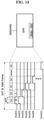
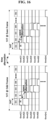
FIGs. 7 ,8 ,14 , and15 , according to an example, when the QHD image is input to thetiming controller 120, thetiming controller 120 may extend the horizontal resolution. Also, in order to extend the vertical resolution by 1.5 times compared to a previous resolution, thetiming controller 120 may control the outputchange circuit unit 132, based on the mode change unit DLG. This may be referred to as a gate line doubling method using a device provided outside the timing controller, so as to extend the vertical resolution. - As illustrated in
FIGs. 14 and15 , when a resolution of an input image corresponds to QHD, the mode change unit DLG may output a first mode change signal DLG1:ON. When the first mode change signal DLG1: ON is output from the mode change unit DLG, the display apparatus may change a driving mode so that a frame is divided into a first group frame and a second group frame and driven. The first group frame and the second group frame may be two continuous frames. Hereinafter, for convenience of description, the first group frame may be defined as an odd frame, and the second group frame may be defined as an even frame. - When the first mode change signal DLG1 : ON is output from the mode change unit DLG, the
shift register 131 may sequentially and divisionally output the gate signals Gout[1] to Gout[m] which are to be supplied to thedisplay panel 150 and may change a position at which one gate signal is output per two gate lines and a position at which one gate signal is output per one gate line. - Therefore, a frame may be divided into an odd frame and an even frame, and two gate lines vertically adjacent to each other may receive one gate signal which is identically generated and then may receive gate signals which are divided and generated, whereby a vertical resolution may be extended by 1.5 times compared to a previous resolution.
- For example, during an odd frame, a first gate line and a second gate line may be simultaneously driven based on one gate signal which is identically generated like "Gout[1] and Gout[2] = H". In this case, subpixels connected with the first gate line and the second gate line may be simultaneously supplied with the same data voltage D1 during 1HT (horizontal time), and thus, a horizontal resolution may be extended by twice compared to a previous resolution. However, during an even frame, the first gate line and the second gate line may be driven at different times, based on two gate signals which are divided and generated like "Gout[1] = H and Gout[2] = L". In this case, the subpixels connected with the first gate line and the second gate line may be simultaneously supplied with different data voltage D1 and D2 at different times during 1HT (horizontal time), and thus, a horizontal resolution may be maintained by once like previous resolution.
- In output patterns of gate signals, during an odd frame, "Gout[1] and Gout[2] = H" may be generated together and then "Gout[3] = H" may be generated, and during an even frame, "Gout[1] = H" may be generated and then "Gout[2] and Gout[3] = H" may be generated together. Such an output pattern may be alternately performed and may be performed up to "Gout[m]".
- In
FIGs. 14 and15 , as theUHD display panel 150 is driven at a driving frequency of 360 Hz, an example may be described where 1VT (vertical time) = 2.77ms@360Hz and 1HT (horizontal time) = 1.87µs. - As illustrated in
FIG. 16 , according to an example, it may be described (time alternation) that output times of gate signals are alternated between an odd frame and an even frame. Also, it may be described (space alternation) that output spaces (positions) of gate signals are alternated whenever frames are alternated. In this case, as seen in "Gout[1] to Gout[3]" or "Gout[4] to Gout[6]," it may be described that space alternation is performed by units of three gate lines which are vertically adjacent to one another and are paired. -
FIGs. 17 to 20 are diagrams for describing a resolution resizing method for displaying a QHD image on an UHD display panel, according to an example of the present disclosure. - As illustrated in
FIGs. 17 and18 , in an example, in order to display a QHD image on a UHD display panel, a horizontal resolution may be extended, a vertical resolution may be reduced, an image may be displayed, and doubling of a gate line may be performed. Here, an extension of the horizontal resolution and a reduction in the vertical resolution may be performed by the timing controller or the image supply unit, and doubling of a gate line may be performed by the gate driver. - A QHD image may be defined as 2560 * 1440. The horizontal resolution may be defined by the number of pixels (2560pxl), and the vertical resolution may be defined by the number of gate lines. Also, 1HT of the QHD image may be 1.3 µs.
- In order to display a QHD image on a UHD display panel, it may be required to extend a horizontal resolution of a UHD image by the number of pixels (3840pxl) defining the horizontal resolution of the UHD image. To this end, the timing controller may extend (2560 -> 3840) the horizontal resolution of the QHD image by 1.5 times through horizontal image processing on the QHD image input thereto. Even when the horizontal resolution of the QHD image is extended, 1HT may maintain 1.3 µs like a previous resolution.
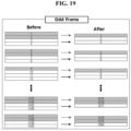
- Unlike an FHD image, it may be difficult to adjust the vertical resolution of the QHD image to the form of the UHD image by using only a gate line doubling method. Therefore, the timing controller may reduce (1440 -> 1080) the vertical resolution of the QHD image to an FHD class through vertical image processing. When the vertical resolution of the QHD image is extended, 1HT may be changed to 1.87 µs, based thereon.
- As described above, when changing of resolution is completely performed on the horizontal resolution and the vertical resolution of the QHD image, the timing controller may control outputs of data signals and gate signals in the form of expressing an image corresponding to 3840 * 1080. As described above, in an example, output patterns of gate signals output from the gate driver may be changed based on the gate line doubling method, and thus, an image displayed on the display panel may finally have a resolution (3840 * 2160) corresponding to the UHD image.
- As illustrated in
FIGs. 19 and20 , in order to reduce (1440 -> 1080) the vertical resolution of the QHD image to the FHD class, a frame may be configured with an odd frame and an even frame, and 1HT may be changed from 1.3 µs to 1.87 µs. - In an odd frame,
images image 1 of the first line, andimages images images images images image 3 of the third line. - Such a method may be implemented as an asymmetrical resolution implementation method which allocates images of four lines as images of three lines and alternately performs the allocation to reduce a vertical resolution to 4:3, thereby minimizing (minimizing a reduction in image quality) the loss of an image in a process of changing the QHD image to the UHD image.
-
FIGs. 21 and 22 are diagrams illustrating some of elements of an apparatus according to an example of the present disclosure. A function and an operation of the apparatus illustrated inFIGs. 21 and 22 are as described above, and thus, elements performing functions and operations and an apparatus including the elements will be mainly described below. - As illustrated in
FIGs. 21 and 22 , a display apparatus according to an example may include an input processor INP, a resolution resizer, and a mode change unit DLG, so as to easily implement an image input at various frequencies and resolutions and minimize a degradation in image quality. - The resolution resizer may extend or reduce a vertical resolution and a horizontal resolution, based on a horizontal scaler and a vertical scaler. Hereinafter, however, for convenience of description, only a horizontal resolution extension unit HOREX and a vertical resolution reduction unit VERRD included in the resolution resizer are illustrated and described.
- When a resolution of a first data signal DATA corresponds to FHD or QHD, the resolution resizer may change a horizontal resolution or a horizontal resolution and a vertical resolution along with image processing needed for driving of the first data signal DATA, and thus, may output a second data signal DDATA.
- For example, when a resolution of the first data signal DATA corresponds to FHD, the resolution resizer may extend only a horizontal resolution of the first data signal DATA by using the horizontal resolution extension unit HOREX, and thus, may output the second data signal DDATA. Also, when a resolution of the first data signal DATA corresponds to QHD, the resolution resizer may extend a horizontal resolution of the first data signal DATA by using the horizontal resolution extension unit HOREX and may reduce a vertical resolution of the first data signal DATA by using the vertical resolution reduction unit VERRD, and thus, may output the second data signal DDATA.
- The resolution resizer, as in
FIG. 21 , may be included in thetiming controller 120, or may be included in theimage supply unit 110 as inFIG. 22 . - In a case which is configured as in
FIG. 21 , the input processor INP may analyze a characteristic (a resolution, a frequency, etc.) of the first data signal DATA and may perform processing based thereon. When it is required to change a resolution on the basis of the characteristic of the first data signal DATA, the input processor INP may transfer the first data signal DATA to the resolution resizer, and when it is not required to change a resolution, the input processor INP may perform only desired image processing and may intactly output (bypass) an image. - For example, when a resolution of the first data signal DATA corresponds to UHD, the input processor INP may bypass image processing so that only image processing needed for driving of the first data signal DATA is performed. In this case, the mode change unit DLG may not output a mode change signal through a signal line DLGS.
- On the other hand, when a resolution of the first data signal DATA corresponds to FHD or QHD, the input processor INP may transfer the first data signal DATA to the resolution resizer so that a resolution is changed. In this case, the mode change unit DLG may output a first mode change signal or a second mode change signal through the signal line DLGS.
- In a case which is configured as in
FIG. 22 , the input processor INP may intactly output the first data signal DATA or the second data signal DDATA. When the first data signal DATA is input, the input processor INP may deactivate the mode change unit DLG so that the mode change signal is not output through the signal line DLGS. On the other hand, when the second data signal DDATA is input, the input processor INP may activate and control the mode change unit DLG so that the first mode change signal or the second mode change signal is output through the signal line DLGS, based on a resolution of an image. - Hereinabove, the present disclosure may easily implement an image input at various frequencies and resolutions and may minimize a degradation in image quality. Also, the present disclosure may easily implement an image input at various frequencies and resolutions, based on an asymmetrical driving method where a display panel is driven alternately in time and space, and may decrease the cost for developing products.
- The effects according to the present disclosure are not limited to the above examples, and other various effects may be included in the specification.
- Further examples are set out in the clauses below:
- 1. A display apparatus comprising: a display panel configured to display an image;
- a gate driver configured to supply gate signals to the display panel;
- a timing controller configured to control an output pattern of the gate driver to cause, in operation, the gate signals to be applied one by one to a set of gate lines, based on an image input from the outside; and a resolution resizer configured to change at least one of a horizontal resolution and a vertical resolution, based on the image input from the outside.
- 1a. A display apparatus comprising: a display panel configured to display an image; a gate driver configured to supply gate signals to the display panel; a timing controller configured to control an output pattern of the gate driver so that the gate signals are applied one by one per one gate line or are applied one by one per two gate lines, based on an image input from the outside; and a resolution resizer configured to change at least one of a horizontal resolution and a vertical resolution, based on the image input from the outside.
- 2. The display apparatus of
clause 1 or 1a, wherein, when an image having a lower resolution than a displayable resolution of the display panel is input, the resolution resizer changes at least one of the horizontal resolution and the vertical resolution, and
the timing controller controls the gate driver so that the output pattern of the gate driver is changed, based on changing of a resolution by the resolution resizer. - 3. The display apparatus of
clause 1 or 1a, wherein there is exactly one gate line in the set of gate lines. - 4. The display apparatus of
clause 1 or la, wherein there are exactly two gate lines in the set of gate lines. - 5. The display apparatus of
clause 4, wherein, when a first image having a lower resolution than a displayable resolution of the display panel is input, the resolution resizer changes the horizontal resolution, and when changing of the horizontal resolution is performed by the resolution resizer, the timing controller controls the gate driver so that the gate signals are applied one by one per at least two gate lines. - 6. The display apparatus of
clause 5, wherein, when a second image having a lower resolution than a displayable resolution of the display panel and a higher resolution than a resolution of the first image is input, the resolution resizer changes the horizontal resolution and the vertical resolution, and
when changing of the horizontal resolution and the vertical resolution is performed by the resolution resizer, the timing controller controls the gate driver so that a portion where the gate signals are applied one by one per one gate line and a portion, where the gate signals are applied one by one per at least two gate lines, are provided. - 7. The display apparatus of
clause 6, wherein, when changing of the horizontal resolution and the vertical resolution is performed by the resolution resizer, the timing controller changes a driving mode so that a frame of the display panel is divided into a first group frame and a second group frame, which are continuous, and driven. - 8. The display apparatus of
clause 6 orclause 7, wherein, based on the dividing of the frame into the first group frame and the second group frame, the timing controller controls the gate driver so that a position of a portion where the gate signals are applied one by one per one gate line and a position of a portion, where the gate signals are applied one by one per at least two gate lines, are alternated. - 9. The display apparatus of
clause 6, wherein a portion where the gate signals are applied one by one per one gate line and a portion, where the gate signals are applied one by one per at least two gate lines, are three gate lines vertically adjacent to one another in the display panel. - 10. A driving method of a display apparatus, the driving method comprising:
- changing at least one of a horizontal resolution and a vertical resolution when an image having a lower resolution than a displayable resolution of a display panel is input; and
- applying gate signals to the display panel one by one per one gate line or either one by one per at least two gate lines, based on the changing of the resolution of the image.
- 11. The driving method of clause 10-, wherein, when the horizontal resolution and the vertical resolution are changed based on the image, there is a first portion of the display where the gate signals are applied one by one per one gate line and there is a second portion of the display where the gate signals are applied one by one per at least two gate lines.
- 12. The driving method of
clause 10 or 11, wherein, when the horizontal resolution and the vertical resolution are changed based on the image, the display panel is driven by dividing a frame into a first group frame and a second group frame which are continuous. - 13. The driving method of any one of clauses 10-12, wherein, based on the dividing of the frame into the first group frame and the second group frame, a position of a portion where the gate signals are applied one by one per one gate line and a position of a portion, where the gate signals are applied one by one per at least two gate lines, are alternated.
- 14. The driving method of clause 13, wherein the first portion where the gate signals are applied one by one per one gate line and the second portion, where the gate signals are applied one by one per at least two gate lines, are three gate lines vertically adjacent to one another in the display panel.
- While the present disclosure has been particularly shown and described with reference to exemplary examples thereof, it will be understood by those of ordinary skill in the art that various changes in form and details may be made therein without departing from the scope of the present disclosure and following claims.
- The various examples described above can be combined to provide further examples. Aspects of the examples can be modified, if necessary to employ concepts of the various patents, applications and publications to provide yet further examples.
- These and other changes can be made to the examples in light of the above-detailed description. In general, in the following claims, the terms used should not be construed to limit the claims to the specific examples disclosed in the specification and the claims, but should be construed to include all possible examples along with the full scope of equivalents to which such claims are entitled. Accordingly, the claims are not limited by the disclosure.
Claims (12)
- A display apparatus comprising:a display panel configured to display an image;a gate driver configured to supply gate signals to the display panel;a timing controller configured to control an output pattern of the gate driver so that the gate signals are applied one by one per one gate line or are applied one by one per two gate lines, based on an image input from the outside; anda resolution resizer configured to change at least one of a horizontal resolution and a vertical resolution, based on the image input from the outside.
- The display apparatus of claim 1, wherein, when an image having a lower resolution than a displayable resolution of the display panel is input, the resolution resizer is configured to change at least one of the horizontal resolution and the vertical resolution, and
the timing controller controls the gate driver configured so that the output pattern of the gate driver is changed, based on changing of a resolution by the resolution resizer. - The display apparatus of claim 1, wherein, when a first image having a lower resolution than a displayable resolution of the display panel is input, the resolution resizer is configured to change the horizontal resolution, and
when changing of the horizontal resolution is performed by the resolution resizer, the timing controller is configured to control the gate driver so that the gate signals are applied one by one per at least two gate lines. - The display apparatus of claim 3, wherein, when a second image having a lower resolution than a displayable resolution of the display panel and a higher resolution than a resolution of the first image is input, the resolution resizer is configured to change the horizontal resolution and the vertical resolution, and
when changing of the horizontal resolution and the vertical resolution is performed by the resolution resizer, the timing controller is configured to control the gate driver so that a portion where the gate signals are applied one by one per one gate line and a portion, where the gate signals are applied one by one per at least two gate lines, are provided. - The display apparatus of claim 4, wherein, when changing of the horizontal resolution and the vertical resolution is performed by the resolution resizer, the timing controller is configured to change a driving mode so that a frame of the display panel is divided into a first group frame and a second group frame, which are continuous, and driven.
- The display apparatus of claim 4 or claim 5, wherein, based on the dividing of the frame into the first group frame and the second group frame, the timing controller is configured to control the gate driver so that a position of a portion where the gate signals are applied one by one per one gate line and a position of a portion, where the gate signals are applied one by one per at least two gate lines, are alternated.
- The display apparatus of claim 4, wherein a portion where the gate signals are applied one by one per one gate line and a portion, where the gate signals are applied one by one per at least two gate lines, are three gate lines vertically adjacent to one another in the display panel.
- A driving method of a display apparatus, the driving method comprising:changing at least one of a horizontal resolution and a vertical resolution when an image having a lower resolution than a displayable resolution of a display panel is input; andapplying gate signals to the display panel one by one per one gate line or either one by one per at least two gate lines, based on the changing of the resolution of the image.
- The driving method of claim 8, wherein, when the horizontal resolution and the vertical resolution are changed based on the image, there is a first portion of the display where the gate signals are applied one by one per one gate line and there is a second portion of the display where the gate signals are applied one by one per at least two gate lines.
- The driving method of claim 8 or claim 9, wherein, when the horizontal resolution and the vertical resolution are changed based on the image, the display panel is driven by dividing a frame into a first group frame and a second group frame which are continuous.
- The driving method of claim any one of claims 8-10, wherein, based on the dividing of the frame into the first group frame and the second group frame, a position of a portion where the gate signals are applied one by one per one gate line and a position of a portion, where the gate signals are applied one by one per at least two gate lines, are alternated.
- The driving method of claim 11, wherein the first portion where the gate signals are applied one by one per one gate line and the second portion, where the gate signals are applied one by one per at least two gate lines, are three gate lines vertically adjacent to one another in the display panel.
Applications Claiming Priority (1)
| Application Number | Priority Date | Filing Date | Title |
|---|---|---|---|
| KR1020220188921A KR20240106224A (en) | 2022-12-29 | 2022-12-29 | Display Device and Driving Method of the same |
Publications (1)
| Publication Number | Publication Date |
|---|---|
| EP4394750A1 true EP4394750A1 (en) | 2024-07-03 |
Family
ID=88757476
Family Applications (1)
| Application Number | Title | Priority Date | Filing Date |
|---|---|---|---|
| EP23208662.9A Pending EP4394750A1 (en) | 2022-12-29 | 2023-11-08 | Display apparatus and driving method thereof |
Country Status (4)
| Country | Link |
|---|---|
| US (1) | US12334021B2 (en) |
| EP (1) | EP4394750A1 (en) |
| KR (1) | KR20240106224A (en) |
| CN (1) | CN118280257A (en) |
Families Citing this family (2)
| Publication number | Priority date | Publication date | Assignee | Title |
|---|---|---|---|---|
| JP2024129959A (en) * | 2023-03-14 | 2024-09-30 | セイコーエプソン株式会社 | Display system, image output device, and program |
| KR20250123305A (en) * | 2024-02-07 | 2025-08-18 | 삼성디스플레이 주식회사 | Display device, and method of operating a display device |
Citations (2)
| Publication number | Priority date | Publication date | Assignee | Title |
|---|---|---|---|---|
| US6088014A (en) * | 1996-05-11 | 2000-07-11 | Hitachi, Ltd. | Liquid crystal display device |
| US20020012006A1 (en) * | 1998-04-07 | 2002-01-31 | Alps Electric Co., Ltd. | Image display device and driver circuit therefor |
Family Cites Families (4)
| Publication number | Priority date | Publication date | Assignee | Title |
|---|---|---|---|---|
| JP2002041023A (en) * | 2000-07-06 | 2002-02-08 | Internatl Business Mach Corp <Ibm> | Computer system, display control device, display device, display control method, recording medium and program transmission device |
| KR101213556B1 (en) * | 2005-12-30 | 2012-12-18 | 엘지디스플레이 주식회사 | Liquid Crystal Display and Method for Driving thereof |
| KR102785187B1 (en) * | 2020-10-12 | 2025-03-21 | 삼성전자주식회사 | Display apparatus and control method thereof |
| KR102746330B1 (en) * | 2020-11-17 | 2024-12-26 | 삼성전자주식회사 | Display apparatus and control method thereof |
-
2022
- 2022-12-29 KR KR1020220188921A patent/KR20240106224A/en active Pending
-
2023
- 2023-11-08 EP EP23208662.9A patent/EP4394750A1/en active Pending
- 2023-11-13 CN CN202311507436.5A patent/CN118280257A/en active Pending
- 2023-11-13 US US18/507,987 patent/US12334021B2/en active Active
Patent Citations (2)
| Publication number | Priority date | Publication date | Assignee | Title |
|---|---|---|---|---|
| US6088014A (en) * | 1996-05-11 | 2000-07-11 | Hitachi, Ltd. | Liquid crystal display device |
| US20020012006A1 (en) * | 1998-04-07 | 2002-01-31 | Alps Electric Co., Ltd. | Image display device and driver circuit therefor |
Also Published As
| Publication number | Publication date |
|---|---|
| US20240221680A1 (en) | 2024-07-04 |
| US12334021B2 (en) | 2025-06-17 |
| CN118280257A (en) | 2024-07-02 |
| KR20240106224A (en) | 2024-07-08 |
Similar Documents
| Publication | Publication Date | Title |
|---|---|---|
| KR100965571B1 (en) | LCD and its driving method | |
| EP2711919B1 (en) | Display driving method | |
| US7710377B2 (en) | LCD panel including gate drivers | |
| CN101075417B (en) | Displaying apparatus using data line driving circuit and data line driving method | |
| KR101703875B1 (en) | LCD and method of driving the same | |
| KR102529503B1 (en) | Display Apparatus and Driving Method of the same | |
| KR101197057B1 (en) | Display device | |
| CN111179798A (en) | Display device and driving method thereof | |
| KR20080006037A (en) | Shift register, display device including same, driving method of shift register and driving method of display device | |
| US20060193002A1 (en) | Drive circuit chip and display device | |
| JP2008116964A (en) | Liquid crystal display device and driving method thereof | |
| JP2001281628A (en) | Liquid crystal display device, portable telephone and portable information terminal device provided with the same | |
| JP2011039205A (en) | Timing controller, image display device, and reset signal output method | |
| CN114446232A (en) | Display driving apparatus and method | |
| US12334021B2 (en) | Display apparatus capable of changing resolution in response to input image and driving method thereof | |
| US8717271B2 (en) | Liquid crystal display having an inverse polarity between a common voltage and a data signal | |
| US12475841B2 (en) | Display apparatus and driving method thereof | |
| KR101497407B1 (en) | Method of driving liquid crystal display device | |
| US20040196242A1 (en) | Active matrix-type display device and method of driving the same | |
| US20070176878A1 (en) | Liquid crystal display device and driving method thereof | |
| KR100891593B1 (en) | LCD and its driving method | |
| KR101343498B1 (en) | Liquid crystal display device | |
| KR101112559B1 (en) | Liquid Crystal Display and Driving Method | |
| KR100927012B1 (en) | LCD and its driving method | |
| KR100855478B1 (en) | LCD panel, driving device and driving method thereof |
Legal Events
| Date | Code | Title | Description |
|---|---|---|---|
| PUAI | Public reference made under article 153(3) epc to a published international application that has entered the european phase |
Free format text: ORIGINAL CODE: 0009012 |
|
| STAA | Information on the status of an ep patent application or granted ep patent |
Free format text: STATUS: REQUEST FOR EXAMINATION WAS MADE |
|
| 17P | Request for examination filed |
Effective date: 20231108 |
|
| AK | Designated contracting states |
Kind code of ref document: A1 Designated state(s): AL AT BE BG CH CY CZ DE DK EE ES FI FR GB GR HR HU IE IS IT LI LT LU LV MC ME MK MT NL NO PL PT RO RS SE SI SK SM TR |
|
| STAA | Information on the status of an ep patent application or granted ep patent |
Free format text: STATUS: EXAMINATION IS IN PROGRESS |