EP4394467A1 - Optical module and optical communication device - Google Patents
Optical module and optical communication device Download PDFInfo
- Publication number
- EP4394467A1 EP4394467A1 EP22861251.1A EP22861251A EP4394467A1 EP 4394467 A1 EP4394467 A1 EP 4394467A1 EP 22861251 A EP22861251 A EP 22861251A EP 4394467 A1 EP4394467 A1 EP 4394467A1
- Authority
- EP
- European Patent Office
- Prior art keywords
- optical
- ics
- fiber bundle
- power supply
- module substrate
- Prior art date
- Legal status (The legal status is an assumption and is not a legal conclusion. Google has not performed a legal analysis and makes no representation as to the accuracy of the status listed.)
- Pending
Links
Images





Classifications
-
- G—PHYSICS
- G02—OPTICS
- G02B—OPTICAL ELEMENTS, SYSTEMS OR APPARATUS
- G02B6/00—Light guides; Structural details of arrangements comprising light guides and other optical elements, e.g. couplings
- G02B6/24—Coupling light guides
- G02B6/42—Coupling light guides with opto-electronic elements
- G02B6/4201—Packages, e.g. shape, construction, internal or external details
- G02B6/4274—Electrical aspects
- G02B6/428—Electrical aspects containing printed circuit boards [PCB]
-
- G—PHYSICS
- G02—OPTICS
- G02B—OPTICAL ELEMENTS, SYSTEMS OR APPARATUS
- G02B6/00—Light guides; Structural details of arrangements comprising light guides and other optical elements, e.g. couplings
- G02B6/24—Coupling light guides
- G02B6/42—Coupling light guides with opto-electronic elements
- G02B6/4201—Packages, e.g. shape, construction, internal or external details
- G02B6/4246—Bidirectionally operating package structures
-
- G—PHYSICS
- G02—OPTICS
- G02B—OPTICAL ELEMENTS, SYSTEMS OR APPARATUS
- G02B6/00—Light guides; Structural details of arrangements comprising light guides and other optical elements, e.g. couplings
- G02B6/24—Coupling light guides
- G02B6/42—Coupling light guides with opto-electronic elements
- G02B6/4201—Packages, e.g. shape, construction, internal or external details
- G02B6/4219—Mechanical fixtures for holding or positioning the elements relative to each other in the couplings; Alignment methods for the elements, e.g. measuring or observing methods especially used therefor
- G02B6/4236—Fixing or mounting methods of the aligned elements
- G02B6/424—Mounting of the optical light guide
-
- G—PHYSICS
- G02—OPTICS
- G02B—OPTICAL ELEMENTS, SYSTEMS OR APPARATUS
- G02B6/00—Light guides; Structural details of arrangements comprising light guides and other optical elements, e.g. couplings
- G02B6/24—Coupling light guides
- G02B6/42—Coupling light guides with opto-electronic elements
- G02B6/4201—Packages, e.g. shape, construction, internal or external details
- G02B6/4249—Packages, e.g. shape, construction, internal or external details comprising arrays of active devices and fibres
-
- G—PHYSICS
- G02—OPTICS
- G02B—OPTICAL ELEMENTS, SYSTEMS OR APPARATUS
- G02B6/00—Light guides; Structural details of arrangements comprising light guides and other optical elements, e.g. couplings
- G02B6/24—Coupling light guides
- G02B6/42—Coupling light guides with opto-electronic elements
- G02B6/4201—Packages, e.g. shape, construction, internal or external details
- G02B6/4266—Thermal aspects, temperature control or temperature monitoring
- G02B6/4268—Cooling
- G02B6/4269—Cooling with heat sinks or radiation fins
-
- G—PHYSICS
- G02—OPTICS
- G02B—OPTICAL ELEMENTS, SYSTEMS OR APPARATUS
- G02B6/00—Light guides; Structural details of arrangements comprising light guides and other optical elements, e.g. couplings
- G02B6/24—Coupling light guides
- G02B6/42—Coupling light guides with opto-electronic elements
- G02B6/4201—Packages, e.g. shape, construction, internal or external details
- G02B6/4285—Optical modules characterised by a connectorised pigtail
-
- G—PHYSICS
- G02—OPTICS
- G02B—OPTICAL ELEMENTS, SYSTEMS OR APPARATUS
- G02B6/00—Light guides; Structural details of arrangements comprising light guides and other optical elements, e.g. couplings
- G02B6/24—Coupling light guides
- G02B6/42—Coupling light guides with opto-electronic elements
- G02B6/4292—Coupling light guides with opto-electronic elements the light guide being disconnectable from the opto-electronic element, e.g. mutually self aligning arrangements
-
- G—PHYSICS
- G02—OPTICS
- G02B—OPTICAL ELEMENTS, SYSTEMS OR APPARATUS
- G02B6/00—Light guides; Structural details of arrangements comprising light guides and other optical elements, e.g. couplings
- G02B6/24—Coupling light guides
- G02B6/42—Coupling light guides with opto-electronic elements
- G02B6/4292—Coupling light guides with opto-electronic elements the light guide being disconnectable from the opto-electronic element, e.g. mutually self aligning arrangements
- G02B6/4293—Coupling light guides with opto-electronic elements the light guide being disconnectable from the opto-electronic element, e.g. mutually self aligning arrangements hybrid electrical and optical connections for transmitting electrical and optical signals
-
- G—PHYSICS
- G02—OPTICS
- G02B—OPTICAL ELEMENTS, SYSTEMS OR APPARATUS
- G02B6/00—Light guides; Structural details of arrangements comprising light guides and other optical elements, e.g. couplings
- G02B6/24—Coupling light guides
- G02B6/42—Coupling light guides with opto-electronic elements
- G02B6/43—Arrangements comprising a plurality of opto-electronic elements and associated optical interconnections
Definitions
- the present disclosure relates to an optical module that performs at least one of conversion from an optical signal to an electrical signal or conversion from an electrical signal to an optical signal, and relates to an optical communication device including the optical module.
- Patent Literature 1 Known devices perform conversion between optical signals and electrical signals (e.g., below-listed Patent Literature 1).
- multiple optical communication devices are attached to a host circuit board.
- Each optical communication device is configured to be capable of being input with and/or outputting multi-channel optical signals.
- optical signals can be transmitted in a number of channels equal to the number of channels of each optical communication device multiplied by the number of optical communication devices using a single host circuit board.
- Each optical communication device is attached to the host circuit board using a connector.
- the printed wiring board may be a double-sided board or a multilayer board on which electronic components (such as the optical ICs 7 in this case) can be mounted on the front and back surfaces.
- a double-sided board includes a board-shaped insulator and conductor layers (not illustrated) stacked on both surfaces of the insulator.
- a multilayer board includes a board-shaped insulator and three or more conductor layers (not illustrated) located on both surfaces of the insulator and inside the insulator.
- the conductor layers may be connected to each other, for example, by solid or hollow via conductors (not illustrated) that penetrate partway through or through the entire thickness of the insulator.
- the optical connector 11 is configured to be removably connected to a mating connector (not illustrated) of an optical waveguide (not illustrated) external to the optical module 1, and is configured to optically connect the optical IC 7 to the external optical waveguide.
- the configurations of the multiple optical connectors 11 are, for example, identical to each other. Unlike in the illustrated example, the configuration of at least some of the optical connectors 11 may be different from the configuration of the other optical connectors 11.
- the number of control ICs 13 may be any number. In the illustrated example, only one control IC 13 is provided, and the one control IC 13 controls all the optical ICs 7. Unlike in the illustrated example, for example, the same number of control ICs 13 as the number of multiple optical ICs 7 may be provided, and one control IC 13 may control only one optical IC 7. In addition, for example, the control ICs 13 may be provided in a number greater than or equal to two but less than the number of optical ICs 7, or the control ICs 13 may be provided in a number greater than the number of optical ICs 7.
- FIG. 3 is a block diagram illustrating an example configuration of a signal processing system of the optical module 1. Here, one optical IC 7, one control IC 13, and one power supply IC 15 are illustrated.
- the optical IC 7 includes, for example, the conversion section 27, which is directly responsible for photoelectric conversion, the processing section 29, which processes electrical signals relating to the conversion section 27, and a sensor 31 that detects temperature.
- the multiple photoelectric conversion elements 33 may be fabricated as separate elements and mounted on the same substrate, or may be fabricated on the same substrate.
- the multiple individual circuits 35 may be fabricated as separate IC chips and mounted on the same substrate, or may be fabricated within a single IC chip.
- the conversion section 27 and the processing section 29 may be fabricated as separate chips and mounted on the same substrate, or may be fabricated in the same chip as each other. This also applies to the sensor 31.
- the sensor 31 outputs an electrical signal corresponding to the temperature to the control IC 13.
- the control IC 13 controls the individual circuits 35 based on the temperature detected by the sensor 31 in order to compensate for changes in the characteristics of the photoelectric conversion elements 33 caused by temperature changes. Specifically, for example, each individual circuit 35 applies a bias to the anode or cathode of the corresponding photoelectric conversion element 33 with a voltage or current according to a value stored in a register thereof.
- the control IC 13 overwrites the value stored in the register in accordance with the value detected by the sensor 31. As a result, changes caused by temperature variations in the relative relationship between the strength of the optical signal and the strength of the electrical signal are reduced.
- control IC 13 is not interposed between the electrical connector 17 and the optical ICs 7.
- the control IC 13 does not have a function of transmitting electrical signals to be converted to optical signal and/or electrical signals converted from optical signals.
- the control IC 13 may have such a function.
- the control IC 13 may also have other functions such as a function of monitoring the current applied to the photoelectric conversion elements 33.
- the optical module 1 may include the module substrate 5, the multiple optical ICs 7, the multiple fiber bundles 9, the multiple optical connectors 11, the at least one control IC 13, and the at least one power supply IC 15.
- the module substrate 5 has a first surface (first mounting surface 5a) that extends in a first direction (y direction) and a second direction (x direction) perpendicular to the first direction.
- the multiple optical ICs 7 are mounted on the first mounting surface 5a at different positions from each other in the y direction and perform photoelectric conversion.
- the multiple fiber bundles 9 each include multiple optical fibers 23 extending in parallel with each other and extending out from the corresponding optical IC 7 toward the first side (+x side) in the second direction.
- the multiple optical connectors 11 are located at the opposite ends of the multiple fiber bundles 9 from the multiple optical ICs 7 and are connected to external optical elements (e.g., optical waveguides, which are not illustrated) and allow transmission of optical signals.
- the at least one control IC 13 is mounted on the module substrate 5 and controls at least one of the multiple optical ICs 7.
- the at least one power supply IC 15 is mounted on the module substrate 5 and supplies power to at least one of the multiple optical ICs 7.
- the transmission bandwidth can be expanded by providing multiple optical ICs 7 that can each transmit multi-channel optical signals.
- size reduction is achieved due to the fact that the multiple optical ICs 7, the control IC 13, and the power supply IC 15 are all mounted on the module substrate 5 and modularized.
- the at least one control IC 13 may include only one control IC 13.
- One control IC 13 may control multiple (all) the optical ICs 7.
- the module substrate 5 can be reduced in size compared to, for example, a mode where the same number of control ICs 13 as the number of the multiple optical ICs 7 are provided (this mode is also included in the technology of the present disclosure). This is due to, for example, the fact that the volume occupied by the packages is reduced by forming a shared package and the gaps between the packages for avoiding short circuits between the packages are eliminated.
- the at least one power supply IC 15 may include one power supply IC.
- One power supply IC 15 may supply power to multiple optical ICs 7.
- the module substrate 5 can be reduced in size similarly to the mode where only one control IC 13 is provided.
- the optical module 1 may further include the cooling component 21 that is in direct or indirect contact with the multiple optical ICs 7 and the module substrate 5, and cools the multiple optical ICs 7 and the module substrate 5.
- optical module 1 Various other examples of the optical module 1 are described below.
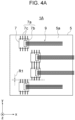
- FIGs. 4A and 4B are schematic plan views illustrating another example and yet another example of the arrangement of the multiple optical ICs 7. That is, these drawings illustrate an optical module 1A of another example and an optical module 1B of yet another example.
- the specific mode to be adopted when shifting multiple optical ICs 7 in the x direction as described above may be chosen as appropriate.
- all of the optical ICs 7 may be displaced with respect to the adjacent optical ICs 7 ( FIG. 4B ), or some of the optical ICs 7 may be displaced with respect to the adjacent optical ICs 7 ( FIG. 4A ).
- the multiple optical ICs 7 are displaced one by one toward opposite sides with respect to each other.
- all the multiple optical ICs 7 are displaced with respect to adjacent optical ICs 7, for example, all the multiple optical ICs 7 are displaced one by one toward the same side.
- Another mode is where a group of two or more optical ICs 7 is displaced toward the same side, and then a group of two or more optical ICs 7 is displaced toward the opposite side from the same side (and then the above two types of displacement are repeated).
- two or more optical ICs 7 in the center (two in the illustrated example) and two or more optical ICs 7 on both sides (two in the illustrated example) are displaced with respect to each other.
- two or more optical ICs 7 on one side in the y direction and at least one optical IC 7 on the other side in the y direction are displaced with respect to each other in the x direction.
- Two optical ICs 7 that are adjacent to each other in the order of arrangement in the y direction and whose positions in the x direction are displaced with respect to each other may overlap each other in terms of the arrangement range in the y direction (an overlapping region R1 may be formed), or, unlike in the illustrated example, might not overlap each other in terms of the arrangement range in the y direction. Even in the latter case, reducing the arrangement range of all the multiple optical ICs 7 in the y direction is easier compared to the mode in FIG. 1 .
- the pin-shaped terminals 7c may overlap each other (illustrated example), or the sealing portions 7b may overlap each other.
- the terminals 7c are pin-shaped for surface mounting, overlapping of the sealing portions 7b is based on the assumption that the pin-shaped terminals 7c overlap.
- the terminals 7c may be, for example, pins for through-hole mounting or pads or bumps for surface mounting, and thus overlapping of the terminals 7c does not need to be based on the assumption that the sealing portions 7b overlap.
- the size of the overlapping region R1 in the y direction may be freely set.
- the number of types of power may be any number.
- the mounting positions of the multiple power supply ICs 15 may be any positions.
- FIG. 5 although the arrangement of the optical ICs 7 in FIG. 4A is taken as an example arrangement, other arrangements are also clearly possible.
- the optical ICs 7 may be located at different positions from each other in the x direction (the direction in which the fiber bundles 9 extend out).
- the lengths of the multiple fiber bundles 9 are identical to each other, the lengths by which the multiple fiber bundles 9 extend out from the edge of the module substrate 5 on the +x side are different from each other. Consequently, the multiple optical connectors 11 are located at different positions from each other. This difference may cause inconveniences depending on the configurations of the devices to which the multiple optical connectors 11 are connected.
- the cooling component 121 includes four wall portions 121b, similarly to the cooling component 21. Cut outs (121ca and 121cb) are formed in the wall portion 121b on the +x side to allow the fiber bundles 9 to extend out of the cooling component 121.
- the cut outs 121cb corresponding to the second fiber bundles 9B are cut out through the wall portion 121b so as to be deeper (longer in the z direction) than the cut outs 121ca corresponding to the first fiber bundles 9A.
- the optical module 1D also includes an auxiliary member 37 fixed to the module substrate 5.
- the auxiliary member 37 includes convex portions 37a that protrude from the first mounting surface 5a of the module substrate 5 toward the +z side and are to be inserted into parts of the cut outs 121cb on the -z side.
- 1 optical module 1 optical module, 3 motherboard (external electronic device), 5 module substrate, 5a first mounting surface (first surface), 7 optical IC, 9 fiber bundle, 11 optical connector, 13 control IC, 15 power supply IC, 17 electrical connector, 23 optical fiber.
Landscapes
- Physics & Mathematics (AREA)
- General Physics & Mathematics (AREA)
- Optics & Photonics (AREA)
- Optical Couplings Of Light Guides (AREA)
Abstract
Description
- The present disclosure relates to an optical module that performs at least one of conversion from an optical signal to an electrical signal or conversion from an electrical signal to an optical signal, and relates to an optical communication device including the optical module.
- Known devices perform conversion between optical signals and electrical signals (e.g., below-listed Patent Literature 1). In
Patent Literature 1, multiple optical communication devices are attached to a host circuit board. Each optical communication device is configured to be capable of being input with and/or outputting multi-channel optical signals. Thus, inPatent Literature 1, optical signals can be transmitted in a number of channels equal to the number of channels of each optical communication device multiplied by the number of optical communication devices using a single host circuit board. Each optical communication device is attached to the host circuit board using a connector. - Patent Literature 1:
Japanese Unexamined Patent Application Publication No. 2003-98392 - In an aspect of the present disclosure, an optical module includes a module substrate, multiple optical ICs, multiple fiber bundles, multiple optical connectors, at least one control IC, and at least one power supply IC. The module substrate has a first surface that extends in a first direction and in a second direction perpendicular to the first direction. The multiple optical ICs are mounted on the first surface at different positions from each other in the first direction and are configured to perform photoelectric conversion. The multiple fiber bundles each include multiple optical fibers extending in parallel with each other. Each of the fiber bundles extends out from a corresponding one of the multiple optical ICs toward a first side in the second direction. The multiple optical connectors are located at opposite ends of the multiple fiber bundles from the multiple optical ICs, are connected to external optical elements, and allow transmission of optical signals. The at least one control IC is mounted on the module substrate and is configured to control at least one of the multiple optical ICs. The at least one power supply IC is mounted on the module substrate and is configured to supply power to at least one of the multiple optical ICs.
- In an aspect of the present disclosure, an optical communication device includes the optical module and a motherboard electrically connected to the optical module.
-
-
FIG. 1 is an exploded perspective view of an optical module according to an embodiment of the present disclosure. -
FIG. 2 is exploded perspective view of the optical module inFIG. 1 from a different direction fromFIG. 1 . -
FIG. 3 is a schematic diagram illustrating an example of the configuration of a signal processing system of part of the optical module inFIG. 1 . -
FIG 4A is a schematic plan view illustrating another example of the arrangement of multiple optical ICs included in an optical module. -
FIG. 4B is a schematic plan view illustrating yet another example of the arrangement of multiple optical ICs included in an optical module. -
FIG. 5 is a schematic plan view illustrating another example of the configuration of a signal processing system of an optical module. -
FIG. 6 is an exploded perspective view illustrating another example of a cooling component of an optical module. -
FIG. 7A is a cross-sectional view taken along line VIIa-VIIa inFIG. 6 . -
FIG. 7B is a cross-sectional view taken along line VIIb-VIIb inFIG. 6 . -
FIG. 7C is a side view of the cooling component inFIG. 6 . -
FIG. 8A is a cross-sectional view illustrating yet another example of a cooling component. -
FIG. 8B is a cross-sectional view illustrating the cooling component inFIG. 8A in a different state from inFIG. 8A . - Hereafter, embodiments of the present disclosure are described while referring to the drawings. The drawings used in the following description are schematic drawings. The dimensional ratios and so on in the drawings do not necessarily match the actual dimensional ratios and so on. In addition, illustration of some details may be omitted and some shapes may be illustrated in an exaggerated manner. A Cartesian coordinate system xyz is added to the drawings for convenience. The relationship between the Cartesian coordinate system xyz and the vertical direction, etc., may be any relationship.
- Hereafter, one embodiment (
FIGs. 1 to 3 ) will be described first, and then various other examples (FIGs. 4A to 8B ) will be described. In the description of the other examples, basically only the differences from the previously described modes (embodiment etc.) will be described. Matters not specifically mentioned may be assumed to be the same as or analogous to the previously described modes. In addition, the description of one mode may be applied to other modes so long as there are no contradictions and so on. -
FIG. 1 is an exploded perspective view of anoptical module 1 of an embodiment of the present disclosure viewed from the +z side.FIG. 2 is an exploded perspective view of theoptical module 1 viewed from the -z side. - The
optical module 1 performs at least one of conversion from optical signals to electrical signals or conversion from electrical signals to optical signals. Theoptical module 1 is configured to allow input and/or output of multi-channel optical signals. - The
optical module 1 is electrically connected to, for example, an external electronic device (e.g., amotherboard 3 represented by dotted lines inFIG. 2 ). In addition, theoptical module 1 is optically connected to an optical element external to the optical module 1 (e.g., an optical waveguide, which is not illustrated). Theoptical module 1 contributes to transmission of signals between themotherboard 3 and a mating device (or a mating device including an optical waveguide, same applies hereafter), which is not illustrated, connected to an end of an optical waveguide. From another perspective, theoptical module 1 contributes to transmission of information between themotherboard 3 and the mating device. - Note that optical waveguides include sheet-like or plate-like structures as well as optical fibers. The
optical module 1 may be optically connected to an external light emitting element or light receiving element without an external optical waveguide interposed therebetween. However, the description of this embodiment may be given under the assumption that theoptical module 1 is connected to an external optical waveguide. The optically connected mating device may be, for example, another electronic device that performs optical communication with the electronic device including themotherboard 3 or may be a device inside the electronic device including themotherboard 3. - The division of roles between the
motherboard 3 and theoptical module 1 may be set as appropriate. For example, theoptical module 1 only contributes to the transmission of information without substantially modifying the information contained in the input and/or output optical signals. Furthermore, theoptical module 1 does not modulate and/or demodulate signals, change the frequencies of the signals, filter the signals, or perform AD conversion of the signals, and only performs photoelectric conversion and amplification of the signals. However, at least some of the processes mentioned above that are not performed by theoptical module 1 may be performed by theoptical module 1. The optical signals and/or electrical signals input to and/or output from theoptical module 1 may be, for example, binary digital signals or signals in other formats. - In order to realize the above operations, the
optical module 1 includes the following components, for example. - ·A
module substrate 5 - ·Multiple (four in the illustrated example)
optical ICs 7 that are mounted on themodule substrate 5 and perform photoelectric conversion - ·Multiple fiber bundles 9 (same number as the optical ICs 7) extending from the multiple
optical ICs 7 - ·Multiple optical connectors 11 (same number as the fiber bundles 9) located on the opposite side of the
multiple fiber bundles 9 from the multipleoptical ICs 7 - ·At least one (one in the illustrated example)
control IC 13 that is mounted on themodule substrate 5 and controls the multipleoptical ICs 7 - ·At least one (one in the illustrated example)
power supply IC 15 that is mounted on themodule substrate 5 and supplies power to the multipleoptical ICs 7 - ·An
electrical connector 17 mounted on themodule substrate 5 and electrically connected to an electronic device external to the optical module 1 (in this case, the motherboard 3) - ·A
passive component 19 mounted on themodule substrate 5 - ·A cooling component 21 (heat sink in the illustrated example) that contributes to cooling of the multiple
optical ICs 7 - Each
fiber bundle 9 includes multiple (four in the illustrated example)optical fibers 23 extending in parallel with each other. In other words, eachoptical IC 7 allows input and/or output of multi-channel optical signals. Theoptical module 1 allows input and/or output of optical signals using a number of channels that is the sum of the numbers of channels of the multipleoptical ICs 7. - The multiple
optical ICs 7 as well as thecontrol IC 13, thepower supply IC 15, and theelectrical connector 17 are mounted on themodule substrate 5. In this way, theoptical module 1 is configured. Therefore, theoptical module 1 is small in size compared to a configuration in which theoptical ICs 7 are attached to a circuit board using connectors, for example. Theoptical module 1 does not need to include thepassive component 19 or thecooling component 21. - In the present disclosure, when ICs (7, 13, 15, etc.) are said to be mounted on the
module substrate 5, the ICs are bonded to themodule substrate 5 using a conductive bonding material (not illustrated) such as solder (including lead-free solder). Therefore, for example, a mode in which the ICs are disposed on themodule substrate 5 so as to be removable by using connectors is not included in the meaning of "mounted" used here. - In present disclosure, when ICs are said to be mounted on the module substrate, the number of ICs may be counted based on units that are directly mounted to the
module substrate 5. For example, all of the multipleoptical ICs 7 are not to be conceptualized as a single IC. Conversely, even if oneoptical IC 7 contains multiple IC chips, that oneoptical IC 7 is not to be regarded as multiple ICs. - Hereafter, referring to
FIGs. 1 and2 , the configurations of the components of theoptical module 1 will be described roughly in the order listed above. After that, while referring toFIG. 3 , an example of the processing performed by theoptical ICs 7 and thecontrol IC 13 will be described. - The
module substrate 5 is, for example, a flat board-shaped member. The front surface and back surface of this flat board are a first mountingsurface 5a and asecond mounting surface 5b, respectively, on which electronic components (such as the optical ICs 7) are mounted. Themodule substrate 5 is composed of, for example, a rigid printed wiring board. The basic configuration (excluding specific configurations according to the arrangement of theoptical ICs 7 and so on) of the rigid printed wiring board may be any of various configurations, for example, may be a known configuration. - For example, the printed wiring board may be a double-sided board or a multilayer board on which electronic components (such as the
optical ICs 7 in this case) can be mounted on the front and back surfaces. A double-sided board includes a board-shaped insulator and conductor layers (not illustrated) stacked on both surfaces of the insulator. A multilayer board includes a board-shaped insulator and three or more conductor layers (not illustrated) located on both surfaces of the insulator and inside the insulator. The conductor layers may be connected to each other, for example, by solid or hollow via conductors (not illustrated) that penetrate partway through or through the entire thickness of the insulator. The conductor layers on the front and back surfaces of the insulator may be partially covered by an insulating film (solder resist). Unlike in the illustrated example, the printed wiring board may be a single-sided board having a conductor layer formed on only one surface of the board-shaped insulator. - For example, in the printed wiring board, the material of the insulator and the material of the conductor may be appropriate materials. For example, the insulator may be composed of an organic material or an inorganic material or a combination of organic and inorganic materials. More specifically, the insulator may be a material consisting of, for example, a base material such as glass cloth impregnated with a resin, or may be a ceramic. The conductor may be a metal such as copper. The conductor layer may, for example, be composed almost entirely of the same material, or may be composed of two or more layers stacked on top of one another, some or all of which are composed of different materials. Via conductors may, for example, be composed entirely of the same material, or may be composed of different materials on the inner side and the outer side thereof.
- The conductors (conductor layers and via conductors), which are not illustrated, of the
module substrate 5 may include parts having appropriate roles. For example, the conductors may include lands on which various electronic components (7, 13, 15, 17, and 19) are mounted and wiring lines that connect the lands to each other. The lands may be pads for surface mounting or may be for through-hole mounting. In addition to the above, the conductors may also include portions constituting electronic elements. An electronic element is, for example, a passive element such as a resistor, an inductor, or a capacitor. - The planar shape and various dimensions of the
module substrate 5 may be set as appropriate in accordance with the number and size of the electronic components (such as the optical ICs 7) to be mounted on themodule substrate 5. In the illustrated example, the planar shape of themodule substrate 5 is a rectangle having four sides parallel to the x direction or the y direction. As an example of the dimensions in a relatively smalloptical module 1, the length of each side of themodule substrate 5 in plan view is greater than or equal to 30 mm and less than or equal to 50 mm. If themodule substrate 5 does not have a rectangular shape, each side of the smallest rectangle encompassing themodule substrate 5 may satisfy the above range of dimensions. - The multiple
optical ICs 7 have identical configurations, for example. Unlike in the illustrated example, the configuration of at least some of theoptical ICs 7 may be different from the configuration of the otheroptical ICs 7 in terms of their internal configuration and/or their externally visible configuration. For example, some of theoptical ICs 7 may be for transmitting optical signals and the remainingoptical ICs 7 may be for receiving optical signals. The number of channels of some of theoptical ICs 7 may be different from the number of channels of the otheroptical ICs 7. For convenience, this embodiment may be described under the assumption that the multipleoptical ICs 7 have identical configurations. - Each
optical IC 7 is, basically, a thin (the length in the z direction is shorter than the lengths in the x direction and y direction) rectangular-parallelepiped-shaped component. A fiber bundle 9 (multiple optical fibers 23) extends out from one surface (+x side) of the rectangular parallelepiped. Theoptical IC 7 performs photoelectric conversion for multiple optical signals carried by the multipleoptical fibers 23. Theoptical IC 7 may include, for example, an electronic element such as a photoelectric conversion element (described later) and apackage 7a that houses the electronic element. The size of the optical IC 7 (package 7a) may be set as appropriate in accordance with the number and diameter of theoptical fibers 23 and the number and size of the electronic elements thereinside. - Except for the point that the
optical fibers 23 extend out of thepackage 7a of theoptical IC 7, the configuration of thepackage 7a of theoptical ICs 7 may be any one of various configurations, for example, may be the same as or similar to a known configuration. For example, the material of a sealingportion 7b of thepackage 7a may be ceramic or resin. Thepackage 7a may be a package to be surface mounted (illustrated example) or a package to be through-hole mounted. In the case of surface mounting,terminals 7c may be pins (illustrated example) or may be pads (or bumps bonded to pads). The shape and number of pins may be any shape and number. In the illustrated example, a mode is illustrated in which pins, serving as terminals, extend out from two side surfaces along the xz plane. In the description of the embodiment, this mode may be assumed for convenience. - The multiple
optical ICs 7 are mounted together on the first mountingsurface 5a of themodule substrate 5. The multipleoptical ICs 7 are mounted so that, for example, the directions in which thefiber bundles 9 extend out are the same as each other. The multipleoptical ICs 7 are mounted at different positions from each other in a direction (y direction) perpendicular to the direction in which thefiber bundles 9 extend, for example, so that themultiple fiber bundles 9 do not overlap each other. In the illustrated example, the multipleoptical ICs 7 are arranged in a single row in the y direction. In other words, the positions of the multipleoptical ICs 7 in the x direction are identical to each other. The pitch of the arrangement is, for example, constant. - When the positions of the electronic components in plan view are said to be the same as or different from each other, for example, this may refer to the positions of the geometric centers of the electronic components in plan view.
- The number of
optical ICs 7 may be any number greater than or equal to two. In the illustrated example, fouroptical ICs 7 are illustrated. This is merely one example, and for example, the number ofoptical ICs 7 may be two or may be ten or more. The number may be odd or even. - The positions and arrangement range and so on of the multiple
optical ICs 7 in the x direction and the y direction may be freely chosen. For example, when themodule substrate 5 is divided into three equal parts in the x direction, eachoptical IC 7 may fit into one of the areas or may straddle two or more areas. The center of eachoptical IC 7 may coincide with the center of themodule substrate 5 in the x direction, or may be located on the +x side or the -x side. The center of the arrangement range of all the multipleoptical ICs 7 in the y direction may coincide with the center of the module substrate in the y direction (illustrated example) or may be located on the +y side or the -y side. - However, from the viewpoint of size reduction, the pitch of the multiple
optical ICs 7 may be relatively small, and the length of themodule substrate 5 in the y direction may be set so that the difference between the length of themodule substrate 5 and the length of the arrangement range of all the multipleoptical ICs 7 in the y direction is small. For example, the pitch of the multipleoptical ICs 7 may be a minimum size at which short circuits do not occur between adjacentoptical ICs 7. The arrangement range in the y direction of all the multiple optical ICs 7 (e.g., the smallest rectangular range encompassing all the optical ICs 7) may be greater than or equal to 2/3, 3/4, or 4/5 of the length of themodule substrate 5 in the y direction. - Unlike in the illustrated example, there may be an
optical IC 7 that is mounted on the second mountingsurface 5b. There may also be anoptical IC 7 from which thefiber bundle 9 extend out in a direction other than toward the +x side. - The configurations of the
multiple fiber bundles 9 are, for example, identical to each other. Unlike in the illustrated example, the configuration of at least some of thefiber bundles 9 may be different from the configuration of theother fiber bundles 9. For example, the number ofoptical fibers 23 included in some of thefiber bundles 9 may be different from the number ofoptical fibers 23 included in theother fiber bundles 9. For example, the length of some of thefiber bundles 9 may be different from the length of theother fiber bundles 9. - In each
fiber bundle 9, the multipleoptical fibers 23 may be bundled together and covered by a sheath, but do not need to be bundled together. In the drawings of the present disclosure, a mode is illustrated in which a sheath is not provided so the fact that thefiber bundle 9 includes theoptical fibers 23 is easily seen. As is clear from the fact that the multipleoptical fibers 23 do not need to be bundled together, the multipleoptical fibers 23 do not need to extend parallel to each other when the multipleoptical fibers 23 are said to extend in parallel with each other. - The number of
optical fibers 23 that eachfiber bundle 9 contains may be any number of two or more. In the illustrated example, fouroptical fibers 23 are illustrated. This is merely one example, and for example, the number ofoptical fibers 23 contained in eachfiber bundle 9 may be two or may be ten or more. The number may be odd or even. - The arrangement of the
optical fibers 23 in the cross-section of eachfiber bundle 9 may be freely chosen. In the illustrated example, all theoptical fibers 23 are arranged in one row in one radial direction (y direction) of theoptical fibers 23, at least inside theoptical IC 7 and inside theoptical connector 11. Within theoptical IC 7, the arrangement direction of theoptical fibers 23 is, for example, the longitudinal direction of a side surface (surface on +x side) of theoptical IC 7, or, from another perspective, a direction along the first mountingsurface 5a of themodule substrate 5. Unlike in the illustrated example, theoptical fibers 23 may be arranged in two or more rows or in a manner that does not conform to the concept of an array. - The configuration of each
optical fiber 23 may be any one of various configurations, for example, may be a known configuration. For example, although not specifically illustrated, theoptical fiber 23 includes a core and a cladding that covers the core and has a higher refractive index than the core. The core and cladding are composed of a translucent material (e.g., quartz glass or plastic). Theoptical fiber 23 may further include a coating composed of a suitable material (e.g., resin or fiber) covering the cladding. For example, theoptical fiber 23 may be a single-mode fiber or a multimode fiber. The diameter of theoptical fiber 23 may be any diameter. - The
optical fiber 23 has, for example, a certain degree of flexibility. Consequently, thefiber bundle 9 is flexible. Therefore, theoptical connector 11 can be oriented in various directions other than the direction illustrated in the drawings. In the illustrated example, the multipleoptical fibers 23 are arrayed in the y direction and so can be relatively easily deformed so as to bend in the z direction. - The
fiber bundle 9 is fixed to theoptical IC 7 in a non-removable manner. In other words, thefiber bundle 9 cannot be separated from theoptical IC 7 without damaging theoptical IC 7. For example, thefiber bundle 9 and the sealingportion 7b are fixed to each other using an adhesive or by being directly adhered to each other and/or by the sealingportion 7b clamping thefiber bundle 9. Thefiber bundle 9 and theoptical connector 11 may be fixed to each other in the same or a similar manner. However, theoptical connector 11 may be composed of two or more members fixed to each other by screws or the like, and part or all of the members may be separable from thefiber bundle 9. - The
optical connector 11 is configured to be removably connected to a mating connector (not illustrated) of an optical waveguide (not illustrated) external to theoptical module 1, and is configured to optically connect theoptical IC 7 to the external optical waveguide. The configurations of the multipleoptical connectors 11 are, for example, identical to each other. Unlike in the illustrated example, the configuration of at least some of theoptical connectors 11 may be different from the configuration of the otheroptical connectors 11. - The configuration of each optical connector 11 (and mating connector) may be any one of various configurations, and for example, may be a known configuration. For example, the
optical connector 11 and the mating connector may be positioned in the radial direction of theoptical fibers 23 by inserting (fitting) one housing into the other housing, and/or may be positioned in the radial direction of theoptical fibers 23 by inserting (fitting) guide pins provided in one connector into guide holes provided in the other connector. The end surfaces of theoptical fibers 23 and the end surfaces of the external optical waveguides may face each other directly or may be optically connected to each other via optical components (e.g., lenses) provided in at least one connector. - The
control IC 13 is mounted on themodule substrate 5 and is electrically connected to at least oneoptical IC 7 via conductors (wiring lines) of themodule substrate 5. Thecontrol IC 13 inputs control signals to the at least oneoptical IC 7. The specific operations of theoptical ICs 7 controlled by thecontrol IC 13 may be any of various operations, and an example is described later with reference toFIG. 3 . - The number of
control ICs 13 may be any number. In the illustrated example, only onecontrol IC 13 is provided, and the onecontrol IC 13 controls all theoptical ICs 7. Unlike in the illustrated example, for example, the same number ofcontrol ICs 13 as the number of multipleoptical ICs 7 may be provided, and onecontrol IC 13 may control only oneoptical IC 7. In addition, for example, thecontrol ICs 13 may be provided in a number greater than or equal to two but less than the number ofoptical ICs 7, or thecontrol ICs 13 may be provided in a number greater than the number ofoptical ICs 7. From another perspective, the number ofoptical ICs 7 controlled by eachcontrol IC 13 may differ from onecontrol IC 13 to anothercontrol IC 13, or two ormore control ICs 13 may control oneoptical IC 7 in different ways from each other. As described above, theoptical module 1 may include at least onecontrol IC 13 that controls at least oneoptical IC 7. - As is clear from the above description, in a mode in which
multiple control ICs 13 are provided, the configurations of themultiple control ICs 13 may be identical to each other or different from each other in terms of the internal configuration and/or the externally visible configuration. The configuration of thecontrol ICs 13 may be any of various configurations, and, for example, may be known configurations, except for specific configurations related to processing contents and so on. The description of thepackage 7a of theoptical IC 7 described above may be applied to the package of the control IC 13 (reference symbol omitted) so long as no contradictions arise. Unlike in the case of theoptical IC 7, thefiber bundles 9 do not extend out from thecontrol IC 13, and therefore, unlike in the illustrated example, thecontrol IC 13 may be provided with pin-shaped terminals (reference symbol omitted) on four side surfaces thereof. - The position at which control
IC 13 is mounted may be any position. In the illustrated example, thecontrol IC 13 is mounted on the first mountingsurface 5a. In other words, thecontrol IC 13 is mounted on the same mounting surface as the mounting surface on which the multipleoptical ICs 7 are mounted. Unlike in the illustrated example, one ormore control ICs 13 may be mounted on the second mountingsurface 5b. Themultiple control ICs 13 may be mounted in a dispersed manner on the first mountingsurface 5a and the second mountingsurface 5b. - The
power supply IC 15 is mounted on themodule substrate 5 and electrically connected to at least oneoptical IC 7 via conductors (wiring lines) of themodule substrate 5. Thepower supply IC 15 supplies power to the at least oneoptical IC 7. - The number of
power supply ICs 15 may be any number. In the illustrated example, only onepower supply IC 15 is provided, and the onepower supply IC 15 supplies power to all theoptical ICs 7. Unlike in the illustrated example, for example, the same number ofpower supply ICs 15 as the number of multipleoptical ICs 7 may be provided, and onepower supply IC 15 may supply power to only oneoptical IC 7. In addition, for example, thepower supply ICs 15 may be provided in a number greater than or equal to two but less than the number ofoptical ICs 7, or thepower supply ICs 15 may be provided in a number greater than the number ofoptical ICs 7. From another perspective, the number ofoptical ICs 7 supplied with power by eachpower supply IC 15 may differ from onepower supply IC 15 to anotherpower supply IC 15, or two or morepower supply ICs 15 may supply different powers to oneoptical IC 7. As described above, theoptical module 1 may include at least onepower supply IC 15 that supplies power to at least oneoptical IC 7. - As is clear from the above description, in a mode in which multiple
power supply ICs 15 are provided, the configurations of the multiplepower supply ICs 15 may be identical to each other or different from each other in terms of the internal configuration and/or the externally visible configuration. The configuration of thepower supply ICs 15 may be any of various configurations, and, for example, may be of any known configuration, except for specific configurations related to role contents and so on. The description of thepackage 7a of theoptical IC 7 described above may be applied to the package of the power supply IC 15 (reference symbol omitted) so long as no contradictions arise. Unlike theoptical ICs 7, thefiber bundles 9 do not extend out from thepower supply IC 15, and therefore, unlike in the illustrated example, thepower supply IC 15 may be provided with pin-shaped terminals (reference symbol omitted) on four side surfaces thereof. - The
power supply IC 15 may be configured, for example, as a DC (Direct Current)/DC converter. For example, thepower supply IC 15 converts DC power supplied from the outside (motherboard 3) via theelectrical connector 17 into DC power of an appropriate voltage or an appropriate current and supplies the DC power to theoptical ICs 7. Thepower supply IC 15 may be a constant voltage power supply or a constant current power supply. Thepower supply IC 15 may be capable of supplying multiple types of power with different voltages or currents from each other, or may be capable of supplying one type of power. Unlike in the above description, thepower supply IC 15 may be a converter other than a DC/DC converter. Thepower supply IC 15 may contribute or not contribute to supplying power to thecontrol IC 13. Unlike in the illustrated example, other power supply ICs may be interposed between theelectrical connector 17 and thepower supply IC 15. - The position where the
power supply IC 15 is mounted may be any position. In the illustrated example, thepower supply IC 15 is mounted on the first mountingsurface 5a. In other words, thepower supply IC 15 is mounted on the same mounting surface as the mounting surface on which the multipleoptical ICs 7 are mounted. Unlike in the illustrated example, one or morepower supply ICs 15 may be mounted on the second mountingsurface 5b (surface on which theoptical ICs 7 are not mounted). The multiplepower supply ICs 15 may be mounted in a dispersed manner on the first mountingsurface 5a and the second mountingsurface 5b. - The
electrical connector 17 is configured to be removably connected to a mating connector (not illustrated) of the motherboard 3 (or of a cable interposed between themotherboard 3 and the optical module 1), and to electrically connect themodule substrate 5 to themotherboard 3. The electrical connector 17 (or, from another perspective, themotherboard 3 connected to the electrical connector 17) is electrically connected to the electronic components mounted on themodule substrate 5 by conductors (wiring lines) of themodule substrate 5. For example, theelectrical connector 17 is connected to theoptical ICs 7, thecontrol IC 13, and thepower supply IC 15 directly or indirectly via other electronic elements. The other electronic elements are, for example, active elements or passive elements mounted on themodule substrate 5 or passive elements composed of conductors of themodule substrate 5. - The number of
electrical connectors 17 may be any number. In the illustrated example, only oneelectrical connector 17 is provided. Unlike in the illustrated example, in a mode in which two or moreelectrical connectors 17 are provided, the two or moreelectrical connectors 17 may be connected to the same device (here, motherboard 3) or may be connected to different devices from each other. - The position at which the
electrical connector 17 is mounted may be any position. In the illustrated example, theelectrical connector 17 is mounted on the second mountingsurface 5b (the surface on which theoptical ICs 7 are not mounted) and fits together with a connector of the mating device in the z direction. Unlike in the illustrated example, one or moreelectrical connectors 17 may be mounted on the first mountingsurface 5a (the surface on which theoptical ICs 7 are mounted), or may be disposed on an edge portion of themodule substrate 5 and fit together with electrical connectors of the mating device in a direction along themodule substrate 5. The multipleelectrical connectors 17 may be mounted in a dispersed manner on the first mountingsurface 5a and the second mountingsurface 5b. - The configuration of each of the electrical connectors 17 (and mating connectors) may be any of various configurations, and for example, may be known configurations. For example, the
electrical connector 17 and the mating connector may be positioned with respect to each other by inserting (fitting) one housing into the other housing and/or by contact between terminals. For example, theelectrical connector 17 and the mating connector may be electrically connected to each other by inserting multiple pin-shaped terminals of one connector into multiple tubular terminals of the other connector, or may be electrically connected to each other by multiple layer-like terminals formed on a surface of a substrate of one connector contacting plate spring terminals provided in recesses of the other connector. - The
passive component 19 is, for example, a resistor, a capacitive element, or an inductor. Onepassive component 19 may be, for example, interposed between any two from among theelectrical connector 17, theoptical ICs 7, thecontrol IC 13, and thepower supply IC 15 and may contribute to impedance matching. The number, function (resistor, capacitive element, or inductor, etc.), shape (chip type, etc.), size, mounting method (surface mounting or through-hole mounting, etc.) and mounting position of thepassive component 19 may be freely chosen. - The cooling component 21 (heat sink) is composed of a material having high heat transfer characteristics. The
cooling component 21 is thermally connected to at least one of themodule substrate 5 or the electronic components mounted on themodule substrate 5 directly or via another material (e.g., grease). In this way, thecooling component 21 contributes to improving the heat dissipation of theoptical module 1. A material having high heat transfer properties is, for example, a metal (e.g., aluminum). The entirety of thecooling component 21 may be, for example, formed of the same material in one piece. Thecooling component 21 is disposed, for example, on the first mountingsurface 5a side with respect to themodule substrate 5. Although not specifically illustrated, instead of or in addition to thecooling component 21, a cooling component may be provided that is disposed on the second mountingsurface 5b side with respect to themodule substrate 5. - The
cooling component 21 may includemultiple fins 21d. Themultiple fins 21d increase the surface area of thecooling component 21 and improve heat dissipation. In the illustrated example, themultiple fins 21d protrude toward the +z side (opposite side of thecooling component 21 from the first mountingsurface 5a) and extend along the first mountingsurface 5a. The thickness (length in the y direction in the illustrated example), height (length in the z direction), extension length (length in the x direction in the illustrated example), direction of extension (x direction or y direction, etc.), pitch, and number offins 21d may be freely chosen. Instead of themultiple fins 21d, multiple pins may be provided that protrude toward the +z side and are disposed two-dimensionally along the xy-plane. - In the illustrated example, the
cooling component 21 is configured to also function as a housing that protects the electronic components (7, 13, and 15, etc.) mounted on the first mountingsurface 5a. Specifically, arecess 21a is formed in a surface of thecooling component 21 facing the first mountingsurface 5a. From another perspective, thecooling component 21 includes an annular wall portion (from another perspective, fourwall portions 21b extending along four sides) extending along the edge of the surface facing the first mountingsurface 5a. Thecooling component 21 is disposed on the first mountingsurface 5a so that the top surfaces (-z-side surfaces) of the fourwall portions 21b contact the first mountingsurface 5a. The electronic components mounted on the first mountingsurface 5a are accommodated in therecess 21a. - Cut
outs 21c are formed in thewall portion 21b on the +x side so as to reduce the height of thewall portion 21b. This allows thefiber bundles 9 to extend out into the space outside thecooling component 21. In the illustrated example,multiple cut outs 21c are formed, with one cut out 21c allowing onefiber bundle 9 to extend out. Unlike in the illustrated example, the number ofcut outs 21c may be one or may be a plural number that is less than the number offiber bundles 9, and one cut out 21c may allow two ormore fiber bundles 9 to extend out. The shape and dimensions of thecut outs 21c may be freely chosen. For example, the depth (length in the z direction) of thecut outs 21c may be smaller than (illustrated example) or equal to the height (length in the z direction) of thewall portion 21b. - The
cooling component 21 may include convex portions 25 (25A to 25D) on the surface facing the first mountingsurface 5a, theconvex portions 25 contributing to contact with the first mountingsurface 5a and/or the electronic components mounted on the first mountingsurface 5a (e.g., the surface on the +z side). In the illustrated example, the multipleconvex portions 25A that individually contact the multipleoptical ICs 7, theconvex portion 25B that contacts thecontrol IC 13, theconvex portion 25C that contacts thepower supply IC 15, and theconvex portion 25D that contacts the first mountingsurface 5a are illustrated. Thewall portions 21b may be taken as examples of theconvex portions 25. Theconvex portions 25 may also be provided in a mode in which thecooling component 21 does not function as a housing. - The shape and size of the
convex portions 25 may be freely chosen. For example, in the illustrated example, oneconvex portion 25 is provided for each IC, but oneconvex portion 25 may contact two or more ICs (of the same type or different types). The area of contact between oneconvex portion 25 and one IC may occupy or not occupy a major portion (e.g., 80% or more) of the area of the top surface (surface on +z side) of the IC. In the illustrated example, theconvex portions control IC 13 and thepower supply IC 15. On the other hand, eachconvex portion 25A is in contact with the top surface of the correspondingoptical IC 7 in planar perspective view so as to overlap a processing section 29 (FIG. 3 described later) but not overlap a conversion section 27 (FIG. 3 below), and the contact area is at least 30% but less than 80% of the area of the top surface of theoptical IC 7. Theconvex portion 25D does not need to be provided, or conversely, may be provided over a wider area than in the illustrated example. - The cooling component 21 (or
convex portions 25 from another perspective) may be in direct contact with the cooling targets (first mountingsurface 5a or electronic components) or may be in indirect contact with the cooling targets via another material. The other material may be grease, for example. The other material may be a sheet having high heat transfer properties and elasticity that is affixed to theconvex portions 25 and/or the cooling targets. The sheet that is affixed to theconvex portions 25 may be considered to be part of theconvex portions 25. Unlike in the illustrated example, the grease and/or sheet may be disposed in order to achieve a thermal connection between the coolingcomponent 21 and the cooling targets without providing theconvex portions 25. In this case, the above description of the contact target and contact area, etc. of theconvex portions 25 may be used for the contact target and contact area, etc. of the grease and/or sheet. - The
cooling component 21 may be fixed to themodule substrate 5 using a suitable method. For example, thecooling component 21 may be fixed using screws (or nuts, if necessary), which are not illustrated, or by an engaging claw. -
FIG. 3 is a block diagram illustrating an example configuration of a signal processing system of theoptical module 1. Here, oneoptical IC 7, onecontrol IC 13, and onepower supply IC 15 are illustrated. - The
optical IC 7 includes, for example, theconversion section 27, which is directly responsible for photoelectric conversion, theprocessing section 29, which processes electrical signals relating to theconversion section 27, and asensor 31 that detects temperature. - The
conversion section 27 includes, for example, the same number ofphotoelectric conversion elements 33 as the number of channels (the number ofoptical fibers 23 connected to one optical IC 7). Thephotoelectric conversion elements 33 are, for example, laser diodes for transmitting optical signals or photodiodes for receiving optical signals. The laser diodes generate an optical signal in response to an electrical signal input from theprocessing section 29 and output the optical signal to theoptical fibers 23. The photodiodes generate an electrical signal in response to an optical signal input from theoptical fibers 23 and output the electrical signal to theprocessing section 29. - The
processing section 29 includes, for example, the same number ofindividual circuits 35 as the number of channels. The multipleindividual circuits 35 are individually (in a one-to-one manner) connected to the multiplephotoelectric conversion elements 33. Theindividual circuits 35 are drive circuits for transmitting optical signals or amplification circuits for receiving optical signals. The drive circuits each output an electrical signal to the correspondingphotoelectric conversion element 33 in response to an electrical signal input from outside theoptical module 1 via theelectrical connector 17. The amplification circuits each amplify an electrical signal input from the correspondingphotoelectric conversion element 33 and output the electrical signal to outside theoptical module 1 via theelectrical connector 17. - The relationship between the above configuration in terms of signal processing and the configuration in terms of the hardware of the
optical ICs 7 may be freely chosen. For example, the multiplephotoelectric conversion elements 33 may be fabricated as separate elements and mounted on the same substrate, or may be fabricated on the same substrate. The multipleindividual circuits 35 may be fabricated as separate IC chips and mounted on the same substrate, or may be fabricated within a single IC chip. Theconversion section 27 and theprocessing section 29 may be fabricated as separate chips and mounted on the same substrate, or may be fabricated in the same chip as each other. This also applies to thesensor 31. - The positional relationship between the
conversion section 27 and theprocessing section 29 in planar perspective view may also be freely chosen. For example, theconversion section 27 may be positioned on the side where thefiber bundle 9 extends out from the optical IC 7 (+x side inFIG. 1 ) with respect to theprocessing section 29. As previously described, thecooling component 21 may directly or indirectly contact the top surface of theoptical IC 7 so as to overlap theprocessing section 29 but not overlap theconversion section 27 in planar perspective view. Of course, unlike in the description above, thecooling component 21 may contact the top surface of theoptical IC 7 so as to overlap theconversion section 27. - The
sensor 31 outputs an electrical signal corresponding to the temperature to thecontrol IC 13. Thecontrol IC 13, for example, controls theindividual circuits 35 based on the temperature detected by thesensor 31 in order to compensate for changes in the characteristics of thephotoelectric conversion elements 33 caused by temperature changes. Specifically, for example, eachindividual circuit 35 applies a bias to the anode or cathode of the correspondingphotoelectric conversion element 33 with a voltage or current according to a value stored in a register thereof. Thecontrol IC 13 overwrites the value stored in the register in accordance with the value detected by thesensor 31. As a result, changes caused by temperature variations in the relative relationship between the strength of the optical signal and the strength of the electrical signal are reduced. - The configuration, number, and location of the
sensor 31 may be freely chosen. For example, thesensor 31 consists of a thermistor or resistance thermometer, and the electrical resistance thereof changes in accordance with temperature. Thesensor 31 may include only a transducer or may include a circuit that performs predetermined processing (e.g., amplification) in addition to the transducer. Only onesensor 31 may be provided for one optical IC 7 (illustrated example), ormultiple sensors 31 may be provided for multiplephotoelectric conversion elements 33 in an individual manner.Multiple sensors 31 may be provided in a number less than the number ofphotoelectric conversion elements 33, and the value detected by thenearest sensor 31 may be used for eachphotoelectric conversion element 33, or a representative value of the detected values may be used. - An example of the above processing may be modified as appropriate. For example, in the above description, the multiple
individual circuits 35 individually apply biases to the multiplephotoelectric conversion elements 33. However, a single circuit may be provided that applies a common bias to the multiplephotoelectric conversion elements 33. For example, instead of theprocessing section 29 inside theoptical IC 7 generating the bias, thecontrol IC 13 may generate the bias. - As mentioned above, in the illustrated example, the
control IC 13 is not interposed between theelectrical connector 17 and theoptical ICs 7. In other words, thecontrol IC 13 does not have a function of transmitting electrical signals to be converted to optical signal and/or electrical signals converted from optical signals. However, thecontrol IC 13 may have such a function. Thecontrol IC 13 may also have other functions such as a function of monitoring the current applied to thephotoelectric conversion elements 33. - As described above, the
optical module 1 may include themodule substrate 5, the multipleoptical ICs 7, themultiple fiber bundles 9, the multipleoptical connectors 11, the at least onecontrol IC 13, and the at least onepower supply IC 15. Themodule substrate 5 has a first surface (first mountingsurface 5a) that extends in a first direction (y direction) and a second direction (x direction) perpendicular to the first direction. The multipleoptical ICs 7 are mounted on the first mountingsurface 5a at different positions from each other in the y direction and perform photoelectric conversion. Themultiple fiber bundles 9 each include multipleoptical fibers 23 extending in parallel with each other and extending out from the correspondingoptical IC 7 toward the first side (+x side) in the second direction. The multipleoptical connectors 11 are located at the opposite ends of themultiple fiber bundles 9 from the multipleoptical ICs 7 and are connected to external optical elements (e.g., optical waveguides, which are not illustrated) and allow transmission of optical signals. The at least onecontrol IC 13 is mounted on themodule substrate 5 and controls at least one of the multipleoptical ICs 7. The at least onepower supply IC 15 is mounted on themodule substrate 5 and supplies power to at least one of the multipleoptical ICs 7. - Therefore, for example, the transmission bandwidth can be expanded by providing multiple
optical ICs 7 that can each transmit multi-channel optical signals. On the other hand, size reduction is achieved due to the fact that the multipleoptical ICs 7, thecontrol IC 13, and thepower supply IC 15 are all mounted on themodule substrate 5 and modularized. - The at least one
control IC 13 may include only onecontrol IC 13. Onecontrol IC 13 may control multiple (all) theoptical ICs 7. - In this case, the
module substrate 5 can be reduced in size compared to, for example, a mode where the same number ofcontrol ICs 13 as the number of the multipleoptical ICs 7 are provided (this mode is also included in the technology of the present disclosure). This is due to, for example, the fact that the volume occupied by the packages is reduced by forming a shared package and the gaps between the packages for avoiding short circuits between the packages are eliminated. - The at least one
power supply IC 15 may include one power supply IC. Onepower supply IC 15 may supply power to multipleoptical ICs 7. - In this case, for example, the
module substrate 5 can be reduced in size similarly to the mode where only onecontrol IC 13 is provided. - The
optical module 1 may further include thecooling component 21 that is in direct or indirect contact with the multipleoptical ICs 7 and themodule substrate 5, and cools the multipleoptical ICs 7 and themodule substrate 5. - In this case, for example, the heat of the multiple
optical ICs 7 can be dissipated by thecooling component 21 over a wide area that covers themodule substrate 5 and optical communication can be stably performed. In addition, for example, as a result of being in contact with both the multipleoptical ICs 7 and themodule substrate 5, the temperature difference between the multipleoptical ICs 7 and themodule substrate 5 can be reduced and the temperature transient period can be reduced. As a result, for example, the probability of unstable optical communication occurring at the time of startup of equipment including theoptical module 1 can be reduced. - Various other examples of the
optical module 1 are described below. -
FIGs. 4A and4B are schematic plan views illustrating another example and yet another example of the arrangement of the multipleoptical ICs 7. That is, these drawings illustrate anoptical module 1A of another example and anoptical module 1B of yet another example. - In these examples, at least one
optical IC 7 is displaced in the x direction with respect to one optical IC 7 (on one side) or two optical ICs 7 (on both sides) that are adjacent thereto in the order of arrangement in the y direction. This allows, for example, there to be a smaller spacing in the y direction between theoptical ICs 7 that are adjacent to each other in the order of arrangement in the y direction. Furthermore, as indicated by an overlapping region R1, adjacentoptical ICs 7 can be made to partially overlap each other in terms of the arrangement range in the y direction. Consequently, the arrangement range in the y direction of all the multipleoptical ICs 7 can be reduced. From another perspective, in the example illustrated inFIG. 1 , the spacing (in the y direction) between adjacentoptical ICs 7 that is for reducing the probability of short circuits is dead space, and such spaces can be reduced. As a result, size reduction of themodule substrate 5 is facilitated. - The specific mode to be adopted when shifting multiple
optical ICs 7 in the x direction as described above may be chosen as appropriate. For example, all of theoptical ICs 7 may be displaced with respect to the adjacent optical ICs 7 (FIG. 4B ), or some of theoptical ICs 7 may be displaced with respect to the adjacent optical ICs 7 (FIG. 4A ). - More specifically, in the example in
FIG. 4B , the multipleoptical ICs 7 are displaced one by one toward opposite sides with respect to each other. As another mode in which all theoptical ICs 7 are displaced with respect to adjacentoptical ICs 7, for example, all the multipleoptical ICs 7 are displaced one by one toward the same side. Another mode is where a group of two or moreoptical ICs 7 is displaced toward the same side, and then a group of two or moreoptical ICs 7 is displaced toward the opposite side from the same side (and then the above two types of displacement are repeated). - In the example in
FIG. 4A , two or moreoptical ICs 7 in the center (two in the illustrated example) and two or moreoptical ICs 7 on both sides (two in the illustrated example) are displaced with respect to each other. As another mode in which some of theoptical ICs 7 are displaced with respect to adjacentoptical ICs 7, for example, two or moreoptical ICs 7 on one side in the y direction and at least oneoptical IC 7 on the other side in the y direction are displaced with respect to each other in the x direction. - Two
optical ICs 7 that are adjacent to each other in the order of arrangement in the y direction and whose positions in the x direction are displaced with respect to each other may overlap each other in terms of the arrangement range in the y direction (an overlapping region R1 may be formed), or, unlike in the illustrated example, might not overlap each other in terms of the arrangement range in the y direction. Even in the latter case, reducing the arrangement range of all the multipleoptical ICs 7 in the y direction is easier compared to the mode inFIG. 1 . - In the mode in which the overlapping region R1 is formed, only the pin-shaped
terminals 7c may overlap each other (illustrated example), or the sealingportions 7b may overlap each other. In the illustrated example, since theterminals 7c are pin-shaped for surface mounting, overlapping of the sealingportions 7b is based on the assumption that the pin-shapedterminals 7c overlap. However, as described previously, theterminals 7c may be, for example, pins for through-hole mounting or pads or bumps for surface mounting, and thus overlapping of theterminals 7c does not need to be based on the assumption that the sealingportions 7b overlap. The size of the overlapping region R1 in the y direction may be freely set. - The two
optical ICs 7 that form the overlapping region R1 and are shifted with respect to each other in the x direction, for example, do not overlap each other in terms of the arrangement range in the x direction. The distance therebetween in the x direction (the size of the gap in the x direction) may be freely set. The twooptical ICs 7 that form the overlapping region R1 can be made to overlap each other in terms of the arrangement range in the x direction. For example, as in the illustrated example, in a mode where theterminals 7c are pins for surface mounting, the terminal 7c furthest toward the +x side is separated from the +x side surface of the sealingportion 7b by a prescribed distance. This also applies to the -x side. Therefore, the x-direction arrangement ranges may overlap each other by a length shorter than the above distance. - In the two
optical ICs 7 forming the overlapping region R1, thefiber bundle 9 extending out from theoptical IC 7 located on the -x side may extend so as to not overlap theoptical IC 7 located on the +x side (illustrated example), or may extend so as to partially overlap in the y direction. In the former case, thefiber bundle 9 may contact or not contact in the y direction theoptical IC 7 on the +x side. In the mode in which part of thefiber bundle 9 extending from theoptical IC 7 on the -x side overlaps theoptical IC 7 on the +x side, thefiber bundle 9 extending from theoptical IC 7 on the -x side and thefiber bundle 9 extending from theoptical IC 7 on the +x side do not overlap each other, for example. - In the case where the external configurations of the
optical ICs 7 adjacent to each other in the order of arrangement in the y direction are not identical to each other, whether or not theoptical ICs 7 are displaced from each other in the x direction may be determined in a rational manner. For example, the geometric centers of the sealingportions 7b (or the smallest virtual rectangles surrounding the sealingportions 7b and theterminals 7c) may be compared to each other in order to determine whether theoptical ICs 7 are displaced from each other. - As described above, at least one
optical IC 7, among the multipleoptical ICs 7, may be displaced in the second direction (x direction, the direction in which thefiber bundle 9 extends out from the optical IC 7) with respect to one or twooptical ICs 7 that are adjacent thereto in the order of arrangement in the first direction (y direction). - In this case, for example, as already described above, size reduction of the
module substrate 5 is facilitated. Theoptical IC 7 located on the +x side (side from which thefiber bundle 9 extends) relative to theoptical IC 7 that is adjacent there to in the order or arrangement in the y direction can function as a member that restricts the movement in the y direction of thefiber bundle 9 extending from the adjacentoptical IC 7. Therefore, not only is size reduction facilitated, but also theoptical IC 7 can be used as a positioning member for thefiber bundle 9. From this perspective as well, size reduction of themodule substrate 5 can achieved. - The at least one
optical IC 7 may be disposed so as to not overlap the one or two adjacentoptical ICs 7 in terms of the arrangement range in the second direction (x direction) and may be disposed so as to partially overlap the one or two adjacentoptical ICs 7 in terms of the arrangement range in the first direction (y direction). - In this case, for example, the effect of reducing the arrangement range of all the multiple
optical ICs 7 in the y direction is improved. Consequently, the effect of facilitating size reduction of themodule substrate 5 is improved. -
FIG. 5 is a schematic plan view of another example relating to thepower supply IC 15. In other words,FIG. 5 illustrates anoptical module 1C according to another example. - In the description of the embodiment, the fact that two or more
power supply ICs 15 may be provided was mentioned. Theoptical module 1C is one example of such a mode. The multiple (three in the illustrated example) power supply ICs 15 (15A, 15B, and 15C) can, for example, supply powers of different voltages (or currents) from each other. Eachpower supply IC 15 also supplies power to multiple (e.g., all)optical ICs 7, as indicated by the dotted lines. Eachoptical IC 7, for example, uses the multiple types of power supplied by the multiplepower supply ICs 15A to 15C for different purposes. For example, theoptical ICs 7 may distribute multiple types of power to at least two or more from among internal core logic circuits, I/O (input/output) circuits, auxiliary logic circuits, circuits applying voltages to thephotoelectric conversion elements 33, and memories. - The number of types of power (number of
power supply ICs 15 in the illustrated example) may be any number. As mentioned in the description of the embodiment, the mounting positions of the multiplepower supply ICs 15 may be any positions. InFIG. 5 , although the arrangement of theoptical ICs 7 inFIG. 4A is taken as an example arrangement, other arrangements are also clearly possible. - As described above, in the
optical module 1C, the at least onepower supply IC 15 may include two or morepower supply ICs 15. The two or morepower supply ICs 15 may supply power of different voltages from each other. Eachpower supply IC 15 may supply power to multipleoptical ICs 7. - In this case, for example, focusing on one type of voltage (or current), each
power supply IC 15 is shared by multipleoptical ICs 7. Therefore, theoptical module 1C can be reduced in size compared to a mode where apower supply IC 15 is provided for eachoptical IC 7 and each voltage (this mode is also included in the technology related to the present disclosure). In addition, compared to the optical module 1 (FIG. 1 ) that includes only onepower supply IC 15, for example, the configuration of thepower supply IC 15 can be simplified and the cost can be reduced. - As illustrated in
FIGs. 4A and4B , theoptical ICs 7 may be located at different positions from each other in the x direction (the direction in which thefiber bundles 9 extend out). In this mode, when the lengths of themultiple fiber bundles 9 are identical to each other, the lengths by which themultiple fiber bundles 9 extend out from the edge of themodule substrate 5 on the +x side are different from each other. Consequently, the multipleoptical connectors 11 are located at different positions from each other. This difference may cause inconveniences depending on the configurations of the devices to which the multipleoptical connectors 11 are connected. Therefore, in an example described below, a regulating member is provided that is for ensuring that the lengths by which themultiple fiber bundles 9 extend out from the edge of themodule substrate 5 on the +x side are equal to each other. In the example described below, the cooling component also serves as the above-mentioned regulating member. This is described more specifically below. -
FIG. 6 is an exploded perspective view illustrating part of anoptical module 1D according to another example.FIG. 7A is a cross-sectional view taken along line VIIa-VIIa inFIG. 6 .FIG. 7B is a cross-sectional view taken along line VIIb-VIIb line inFIG. 6 .FIG. 7C is a side view of theoptical module 1D seen from the +x side (but thefiber bundle 9 is illustrated in cross-section). - As illustrated in
FIG. 6 , in the description here, the arrangement illustrated inFIG. 4A is taken as an example of the arrangement of the multipleoptical ICs 7. However, the arrangement of the multipleoptical ICs 7 may be another arrangement. Acooling component 121 of theoptical module 1D may includemultiple fins 21d (or multiple pins) andconvex portions 25, similarly to thecooling component 21. However, the illustration of such parts is omitted here. - In the following description, for convenience, the
fiber bundles 9 extending out from theoptical ICs 7 located relatively on the -x side may be referred to asfirst fiber bundles 9A. The fiber bundles 9 extending out from theoptical ICs 7 located relatively on the +x side may be referred to assecond fiber bundles 9B. Theoptical connectors 11 provided on thefirst fiber bundles 9A may be referred to as firstoptical connectors 11A. Theoptical connectors 11 provided on thesecond fiber bundles 9B may be referred to as secondoptical connectors 11B. - As illustrated in
FIG. 7A , eachfirst fiber bundle 9A, for example, extends from the correspondingoptical IC 7 in a generally straight line to the edge of themodule substrate 5 on the +x side. On the other hand, as illustrated inFIG. 7B , eachsecond fiber bundle 9B is bent partway therealong and extends to the end of themodule substrate 5 on the +x side (in planar perspective view). In other words, thesecond fiber bundle 9B more greatly deviates from a straight line shape than thefirst fiber bundle 9A, and thus the difference in length from theoptical IC 7 to the edge of themodule substrate 5 between the two bundles is less than the difference between the positions in the x direction (positions of side surfaces on +x side) of theoptical ICs 7 to which the bundles are connected. - The above difference between the paths of the
fiber bundles 9 may be realized via bending in any direction, and in the illustrated example, is realized via bending in the z direction. The number of bends may be any number. From another perspective, the number of positions at which thecooling component 121 regulates the paths of thefiber bundles 9 may be freely chosen. In the illustrated example, thefirst fiber bundle 9A extends in a straight line, but thefirst fiber bundle 9A may also be bent at an appropriate position. From another perspective, thecooling component 121 may only regulate the length by which thesecond fiber bundles 9B extend out from themodule substrate 5, or additionally, may regulate the length by which thefirst fiber bundles 9A extend out from themodule substrate 5. - Various configurations for allowing the
cooling component 121 to regulate (restrict) at least part of the path of at least some of thefiber bundles 9 can be adopted. The illustrated example is configured as follows. - As illustrated in
FIG. 6 , thecooling component 121 includes fourwall portions 121b, similarly to thecooling component 21. Cut outs (121ca and 121cb) are formed in thewall portion 121b on the +x side to allow thefiber bundles 9 to extend out of thecooling component 121. The cut outs 121cb corresponding to thesecond fiber bundles 9B are cut out through thewall portion 121b so as to be deeper (longer in the z direction) than the cut outs 121ca corresponding to thefirst fiber bundles 9A. Theoptical module 1D also includes anauxiliary member 37 fixed to themodule substrate 5. Theauxiliary member 37 includesconvex portions 37a that protrude from the first mountingsurface 5a of themodule substrate 5 toward the +z side and are to be inserted into parts of the cut outs 121cb on the -z side. - Therefore, when the
cooling component 121 is attached to themodule substrate 5, as illustrated inFIG. 7C , opening are formed at the height of the first mountingsurface 5a that allow thefirst fiber bundles 9A to pass therethrough, and openings are formed that allow thesecond fiber bundles 9B to pass therethrough, these openings being formed further toward the +z side than the former openings. Both sets of openings are, for example, equivalent in shape and size to each other. Theauxiliary member 37 may be regarded as a part of thecooling component 121 or as a separate member from thecooling component 121. For convenience, the following description is based on the latter assumption. In either case, thecooling component 121 functions as a regulating member that restricts the paths of the fiber bundles 9. - As illustrated in
FIG. 7B , thecooling component 121 includes aconvex portion 121f protruding from the surface facing the first mountingsurface 5a toward the -z side. Theconvex portion 121f contacts part of thesecond fiber bundle 9B that extends from theoptical IC 7 to the cut out 121cb from the +z side so as to restrict the path of thesecond fiber bundle 9B. Accordingly, thesecond fiber bundle 9B bends toward the +z side at the position of theconvex portion 121f and extends into the cut out 121cb. - As illustrated in
FIG. 7A , let us assume a situation in which the firstoptical connector 11A is positioned toward the +x side to the maximum extent. Furthermore, as illustrated inFIG. 7B , let us assume a situation in which the secondoptical connector 11B is positioned toward the +x side to the maximum extent provided that the z-direction position of the secondoptical connector 11B is aligned with the z-direction position of the firstoptical connector 11A. In this case, the x-direction position of the firstoptical connector 11A and the x-direction position of the secondoptical connector 11B may, for example, be roughly aligned. For example, the difference between the optical connectors may be less than or equal to 1/3 or less than or equal to 1/5 of the difference between the x-direction positions of theoptical IC 7 on the -x side and theoptical IC 7 on the +x side. - Let us assume a situation in which each of the first
optical connector 11A and the secondoptical connector 11B are both positioned towards the +x side to the maximum extent. In other words, unlike inFIG. 7B , let us assume a situation in which thesecond fiber bundle 9B is made to extend parallel to the x direction from the position of the opening formed by the cut out 121cb. In this case, the difference between the x-direction position of the firstoptical connector 11A and the x-direction position of the secondoptical connector 11B is smaller than, for example, the difference between the x-direction positions of theoptical IC 7 on the - x side and theoptical IC 7 on the +x side. The length by which thefiber bundle 9 extends out from the +x-side edge of themodule substrate 5 in the situation assumed here is an example of an extension length described below. - Unlike in the illustrated example, the positions in the z direction when the
first fiber bundle 9A and thesecond fiber bundle 9B extend out from the +x-side edge of the module substrate 5 (extending out from the cut outs in the cooling component 121) may be the same for thefirst fiber bundle 9A and thesecond fiber bundle 9B. In other words, the length by which thesecond fiber bundle 9B extends out from the +x-side edge of themodule substrate 5 may be adjusted by forming convex portions on the -z-side surface of thecooling component 21 and/or the first mountingsurface 5a as appropriate while keeping the shape and size of the cut outs 121ca and 121cb identical. -
FIGs. 8A and 8B correspond toFIGs. 7A and 7B and illustrate yet another example. - In a
cooling component 121A in this example, the cut outs that thefirst fiber bundle 9A and thesecond fiber bundle 9B extend through are the cut outs 121ca illustrated inFIG. 6 . In other words, thefirst fiber bundle 9A and thesecond fiber bundle 9B pass through openings at the same height as each other. Each of thefirst fiber bundle 9A and thesecond fiber bundle 9B is provided with astopper 39. The length of thefiber bundle 9 from theoptical connector 11 to thestopper 39 is identical for thefirst fiber bundle 9A and thesecond fiber bundle 9B. The position of thestopper 39 in the x direction is restricted by the opening formed by the cut out 121ca. Thecooling component 121 may regulate part of the path of thefiber bundle 9 in this manner. - As described above, the
optical module 1D may include a regulating member (coolingcomponent 121 and auxiliary member 37) that regulates the path of at least part of at least onefiber bundle 9 among themultiple fiber bundles 9. The multipleoptical ICs 7 may include a first optical IC (optical IC 7 on the -x side) and a second optical IC (optical IC 7 on the +x side) located further toward the first side (the side from which thefiber bundle 9 extends. +x side) than the first optical IC. Themultiple fiber bundles 9 may include afirst fiber bundle 9A extending out from the -x-sideoptical IC 7 and asecond fiber bundle 9B extending out from the +x-sideoptical IC 7. The length of eachfiber bundle 9 from the correspondingoptical IC 7 to the correspondingoptical connector 11 will be referred to as a total length. The length by which eachfiber bundle 9 can extend out toward the +x side parallel to the first direction (x direction) from the +x side edge of themodule substrate 5 will be referred to as an extension length. Thefirst fiber bundle 9A and thesecond fiber bundle 9B may have the same total length as each other. The regulating member (coolingcomponent 121 and auxiliary member 37) may regulate the path of at least part of at least thesecond fiber bundle 9B so that the difference between the extension length of thefirst fiber bundle 9A and the extension length of thesecond fiber bundle 9B is smaller than the difference between the positions in the x direction of theoptical IC 7 on the -x side and theoptical IC 7 on the +x side. - In this case, for example, as already described above, in a mode where the positions of the
optical ICs 7 in the x direction are different from each other and the lengths of thefiber bundles 9 are identical to each other, the difference between the positions of theoptical connectors 11 can be reduced and convenience is improved. From another perspective, the need to make the lengths of themultiple fiber bundles 9 different from each other in order to make the positions of theoptical connectors 11 identical to each other (such a mode is also included in the technology according to the present disclosure) is reduced. As a result, for example, the configurations of themultiple fiber bundles 9, etc. can be made identical to each other and productivity can be improved. - The above-mentioned regulating member may be in contact with the multiple
optical ICs 7 and may cool the multipleoptical ICs 7. In other words, at least part of regulating member may consist of thecooling component 121. - In this case, for example, the
cooling component 121 also serves as the regulating member, and as a result, theoptical module 1D is simplified, and this in turn, results in a reduction in size. - The technology according to present disclosure is not limited to the above embodiment and different examples, and may be implemented in various modes.
- For example, not only a fiber bundle but also wiring for transmitting electrical signals may extend out from the optical ICs. In this case, separate connectors may be provided for the fiber bundles and wiring, or shared connectors may be provided. In other words, for the latter case, an optical connector may also serve as an electrical connector. The cooling component may be a Peltier element rather than a heat sink.
- Different concepts can be extracted from present disclosure than the concept of mounting multiple optical ICs, at least one control IC, at least one power supply IC, and an electrical connector together on a module substrate. For example, techniques for shifting the positions of multiple optical ICs from each other in the second direction or adjusting the lengths of multiple fiber bundles by means of a cooling component do not need to be premised on the requirement that the control IC and power supply IC are mounted on a module substrate together with the optical ICs.
- 1 optical module, 3 motherboard (external electronic device), 5 module substrate, 5a first mounting surface (first surface), 7 optical IC, 9 fiber bundle, 11 optical connector, 13 control IC, 15 power supply IC, 17 electrical connector, 23 optical fiber.
Claims (10)
- An optical module comprising:a module substrate having a first surface that extends in a first direction and a second direction perpendicular to the first direction;multiple optical ICs mounted on the first surface at different positions from each other in the first direction and configured to perform photoelectric conversion;multiple fiber bundles each including multiple optical fibers extending in parallel with each other, each of the fiber bundles extending out from a corresponding one of the multiple optical ICs toward a first side in the second direction;multiple optical connectors located at opposite ends of the multiple fiber bundles from the multiple optical ICs, connected to external optical elements, and configured to allow transmission of optical signals;at least one control IC mounted on the module substrate and configured to control at least one of the multiple optical ICs; andat least one power supply IC mounted on the module substrate and configured to supply power to at least one of the multiple optical ICs.
- The optical module according to claim 1, wherein, among the multiple optical ICs, at least one optical IC is displaced in the second direction with respect to one or two optical ICs that are adjacent thereto in order of arrangement in the first direction.
- The optical module according to claim 2, wherein the at least one optical IC does not overlap the adjacent one or two optical ICs in terms of an arrangement range in the second direction, but does partially overlap the adjacent one or two optical ICs in terms of an arrangement range in the first direction.
- The optical module according to any one of claims 1 to 3, wherein the at least one control IC includes only one control IC, and
the one control IC is configured to control the multiple optical ICs. - The optical module according to any one of claims 1 to 4, wherein the at least one power supply IC includes only one power supply IC, and
the one power supply IC is configured to supply power to the multiple optical ICs. - The optical module according to any one of claims 1 to 4, wherein the at least one power supply IC includes two or more power supply ICs, and
the two or more power supply ICs are configured to supply powers of different voltages from each other and are configured to each supply power to the multiple optical ICs. - The optical module according to any one of claims 1 to 6, further comprising:
a cooling component that is in direct or indirect contact with the multiple optical ICs and the module substrate and is configured to cool the multiple optical ICs and the module substrate. - The optical module according to any one of claims 1 to 7, further comprising:a regulating member configured to regulate a path of at least part of at least one fiber bundle among the multiple fiber bundles,wherein the multiple optical ICs includea first optical IC, anda second optical IC is located toward the first side relative to the first optical IC,the multiple fiber bundles includea first fiber bundle extending from the first optical IC, anda second fiber bundle extending from the second optical IC,when a length of each of the fiber bundles from the corresponding optical IC to the corresponding optical connector is called a total length, and a length by which each fiber bundle can extend out parallel to the second direction from an edge, on the first side, of the module substrate is called an extension length,the first fiber bundle and the second fiber bundle have identical total lengths, andthe regulating member is configured to regulate a path of at least part of at least the second fiber bundle and make a difference between the extension length of the first fiber bundle and the extension length of the second fiber bundle smaller than a difference between positions of the first optical IC and the second optical IC in the first direction.
- The optical module according to claim 8, wherein the regulating member is in contact with the multiple optical ICs and is configured to cool the multiple optical ICs.
- An optical communication device comprising:the optical module according to any one of claims 1 to 9, anda motherboard electrically connected to the optical module.
Applications Claiming Priority (2)
| Application Number | Priority Date | Filing Date | Title |
|---|---|---|---|
| JP2021138893 | 2021-08-27 | ||
| PCT/JP2022/031300 WO2023026963A1 (en) | 2021-08-27 | 2022-08-19 | Optical module and optical communication device |
Publications (2)
| Publication Number | Publication Date |
|---|---|
| EP4394467A1 true EP4394467A1 (en) | 2024-07-03 |
| EP4394467A4 EP4394467A4 (en) | 2025-08-13 |
Family
ID=85322113
Family Applications (1)
| Application Number | Title | Priority Date | Filing Date |
|---|---|---|---|
| EP22861251.1A Pending EP4394467A4 (en) | 2021-08-27 | 2022-08-19 | OPTICAL MODULE AND OPTICAL COMMUNICATION DEVICE |
Country Status (5)
| Country | Link |
|---|---|
| US (1) | US20240310591A1 (en) |
| EP (1) | EP4394467A4 (en) |
| JP (2) | JP7631536B2 (en) |
| CN (1) | CN117836685A (en) |
| WO (1) | WO2023026963A1 (en) |
Families Citing this family (1)
| Publication number | Priority date | Publication date | Assignee | Title |
|---|---|---|---|---|
| CN117055177A (en) * | 2023-08-03 | 2023-11-14 | 江苏奥雷光电有限公司 | Heat dissipation design method for high-speed high-power optical module |
Family Cites Families (10)
| Publication number | Priority date | Publication date | Assignee | Title |
|---|---|---|---|---|
| JPH08262277A (en) * | 1995-03-23 | 1996-10-11 | Sumitomo Electric Ind Ltd | Parallel optical interconnection device |
| JP3405402B2 (en) * | 1999-06-23 | 2003-05-12 | 日本電気株式会社 | Parallel transmission type optical module and method of manufacturing the same |
| JP2003098392A (en) | 2001-09-26 | 2003-04-03 | Hitachi Cable Ltd | Optical communication device |
| WO2011136819A1 (en) * | 2010-04-30 | 2011-11-03 | Hewlett-Packard Development Company, L.P. | Circuit module |
| JP5644574B2 (en) * | 2011-02-18 | 2014-12-24 | 日本電気株式会社 | Optical module and optical module mounting substrate |
| JP6115067B2 (en) * | 2012-10-05 | 2017-04-19 | 富士通株式会社 | Optical module |
| JP2016031990A (en) * | 2014-07-28 | 2016-03-07 | 日立金属株式会社 | Photo-electric conversion module and transmission device including photo-electric conversion module |
| US10866376B1 (en) * | 2019-06-26 | 2020-12-15 | Ali Ghiasi | Method and system for co-packaging photonics integrated circuit with an application specific integrated circuit |
| WO2021076649A1 (en) * | 2019-10-15 | 2021-04-22 | Ayar Labs, Inc. | Multi-chip packaging of silicon photonics |
| CN111511097B (en) * | 2020-06-18 | 2020-12-29 | 深圳市欧博凯科技有限公司 | High-speed transmission optical module circuit board structure and manufacturing method thereof, and anti-crosstalk method |
-
2022
- 2022-08-19 JP JP2023543868A patent/JP7631536B2/en active Active
- 2022-08-19 EP EP22861251.1A patent/EP4394467A4/en active Pending
- 2022-08-19 US US18/681,247 patent/US20240310591A1/en active Pending
- 2022-08-19 CN CN202280054099.6A patent/CN117836685A/en active Pending
- 2022-08-19 WO PCT/JP2022/031300 patent/WO2023026963A1/en not_active Ceased
-
2025
- 2025-02-05 JP JP2025017264A patent/JP2025069372A/en active Pending
Also Published As
| Publication number | Publication date |
|---|---|
| JP7631536B2 (en) | 2025-02-18 |
| JP2025069372A (en) | 2025-04-30 |
| WO2023026963A1 (en) | 2023-03-02 |
| CN117836685A (en) | 2024-04-05 |
| US20240310591A1 (en) | 2024-09-19 |
| JPWO2023026963A1 (en) | 2023-03-02 |
| EP4394467A4 (en) | 2025-08-13 |
Similar Documents
| Publication | Publication Date | Title |
|---|---|---|
| CN103370644B (en) | Optical circuit board | |
| US8669515B2 (en) | Photoelectric conversion module | |
| JP4825739B2 (en) | Structure of opto-electric hybrid board and opto-electric package | |
| US7470069B1 (en) | Optoelectronic MCM package | |
| US7137744B2 (en) | Fiber optic transceiver module with rigid and flexible circuit boards | |
| US7488119B2 (en) | Photoelectric composite connector and substrate using the same | |
| US11415764B2 (en) | Optical module | |
| US20110031379A1 (en) | Photoelectric conversion module | |
| US10025049B2 (en) | Optoelectrical connector module | |
| US20190182949A1 (en) | Flexible printed circuit board and optical module | |
| US12130483B2 (en) | Optical module | |
| US12571969B2 (en) | Optical module having electrically-connected substrate | |
| EP4394467A1 (en) | Optical module and optical communication device | |
| CN118901131A (en) | Baseboard components | |
| CN118591748A (en) | An optical module | |
| US20190129113A1 (en) | Optical engine and optical module | |
| US10830972B2 (en) | Optical connector, electronic apparatus and optical interconnection system | |
| WO2022255829A1 (en) | Laser diode package | |
| JP7699667B2 (en) | Optical module and optical communication device | |
| US20250189735A1 (en) | Optical device and optical transceiver | |
| US20210399805A1 (en) | Optical transceiver | |
| JP2002261372A (en) | Mounting board and optical module | |
| US7307438B2 (en) | Thermal transferring member, test board and test apparatus | |
| US20240118503A1 (en) | Opto-electric composite transmission module | |
| JP3792998B2 (en) | Optical data link module and assembly method thereof |
Legal Events
| Date | Code | Title | Description |
|---|---|---|---|
| STAA | Information on the status of an ep patent application or granted ep patent |
Free format text: STATUS: THE INTERNATIONAL PUBLICATION HAS BEEN MADE |
|
| PUAI | Public reference made under article 153(3) epc to a published international application that has entered the european phase |
Free format text: ORIGINAL CODE: 0009012 |
|
| STAA | Information on the status of an ep patent application or granted ep patent |
Free format text: STATUS: REQUEST FOR EXAMINATION WAS MADE |
|
| 17P | Request for examination filed |
Effective date: 20240205 |
|
| AK | Designated contracting states |
Kind code of ref document: A1 Designated state(s): AL AT BE BG CH CY CZ DE DK EE ES FI FR GB GR HR HU IE IS IT LI LT LU LV MC MK MT NL NO PL PT RO RS SE SI SK SM TR |
|
| DAV | Request for validation of the european patent (deleted) | ||
| DAX | Request for extension of the european patent (deleted) | ||
| A4 | Supplementary search report drawn up and despatched |
Effective date: 20250716 |
|
| RIC1 | Information provided on ipc code assigned before grant |
Ipc: G02B 6/42 20060101AFI20250710BHEP Ipc: G02B 6/43 20060101ALI20250710BHEP |