EP4394459A1 - Electronic device - Google Patents
Electronic device Download PDFInfo
- Publication number
- EP4394459A1 EP4394459A1 EP22860375.9A EP22860375A EP4394459A1 EP 4394459 A1 EP4394459 A1 EP 4394459A1 EP 22860375 A EP22860375 A EP 22860375A EP 4394459 A1 EP4394459 A1 EP 4394459A1
- Authority
- EP
- European Patent Office
- Prior art keywords
- liquid lens
- region
- substrate layer
- screen substrate
- electronic device
- Prior art date
- Legal status (The legal status is an assumption and is not a legal conclusion. Google has not performed a legal analysis and makes no representation as to the accuracy of the status listed.)
- Pending
Links
Images


Classifications
-
- G—PHYSICS
- G02—OPTICS
- G02B—OPTICAL ELEMENTS, SYSTEMS OR APPARATUS
- G02B3/00—Simple or compound lenses
- G02B3/12—Fluid-filled or evacuated lenses
- G02B3/14—Fluid-filled or evacuated lenses of variable focal length
-
- G—PHYSICS
- G02—OPTICS
- G02B—OPTICAL ELEMENTS, SYSTEMS OR APPARATUS
- G02B26/00—Optical devices or arrangements for the control of light using movable or deformable optical elements
- G02B26/004—Optical devices or arrangements for the control of light using movable or deformable optical elements based on a displacement or a deformation of a fluid
-
- H—ELECTRICITY
- H04—ELECTRIC COMMUNICATION TECHNIQUE
- H04N—PICTORIAL COMMUNICATION, e.g. TELEVISION
- H04N23/00—Cameras or camera modules comprising electronic image sensors; Control thereof
- H04N23/50—Constructional details
-
- H—ELECTRICITY
- H04—ELECTRIC COMMUNICATION TECHNIQUE
- H04N—PICTORIAL COMMUNICATION, e.g. TELEVISION
- H04N23/00—Cameras or camera modules comprising electronic image sensors; Control thereof
- H04N23/50—Constructional details
- H04N23/54—Mounting of pick-up tubes, electronic image sensors, deviation or focusing coils
-
- H—ELECTRICITY
- H04—ELECTRIC COMMUNICATION TECHNIQUE
- H04N—PICTORIAL COMMUNICATION, e.g. TELEVISION
- H04N23/00—Cameras or camera modules comprising electronic image sensors; Control thereof
- H04N23/50—Constructional details
- H04N23/55—Optical parts specially adapted for electronic image sensors; Mounting thereof
-
- H—ELECTRICITY
- H04—ELECTRIC COMMUNICATION TECHNIQUE
- H04N—PICTORIAL COMMUNICATION, e.g. TELEVISION
- H04N23/00—Cameras or camera modules comprising electronic image sensors; Control thereof
- H04N23/57—Mechanical or electrical details of cameras or camera modules specially adapted for being embedded in other devices
-
- H—ELECTRICITY
- H04—ELECTRIC COMMUNICATION TECHNIQUE
- H04N—PICTORIAL COMMUNICATION, e.g. TELEVISION
- H04N23/00—Cameras or camera modules comprising electronic image sensors; Control thereof
- H04N23/60—Control of cameras or camera modules
-
- G—PHYSICS
- G02—OPTICS
- G02F—OPTICAL DEVICES OR ARRANGEMENTS FOR THE CONTROL OF LIGHT BY MODIFICATION OF THE OPTICAL PROPERTIES OF THE MEDIA OF THE ELEMENTS INVOLVED THEREIN; NON-LINEAR OPTICS; FREQUENCY-CHANGING OF LIGHT; OPTICAL LOGIC ELEMENTS; OPTICAL ANALOGUE/DIGITAL CONVERTERS
- G02F1/00—Devices or arrangements for the control of the intensity, colour, phase, polarisation or direction of light arriving from an independent light source, e.g. switching, gating or modulating; Non-linear optics
- G02F1/01—Devices or arrangements for the control of the intensity, colour, phase, polarisation or direction of light arriving from an independent light source, e.g. switching, gating or modulating; Non-linear optics for the control of the intensity, phase, polarisation or colour
- G02F1/13—Devices or arrangements for the control of the intensity, colour, phase, polarisation or direction of light arriving from an independent light source, e.g. switching, gating or modulating; Non-linear optics for the control of the intensity, phase, polarisation or colour based on liquid crystals, e.g. single liquid crystal display cells
- G02F1/133—Constructional arrangements; Operation of liquid crystal cells; Circuit arrangements
- G02F1/1333—Constructional arrangements; Manufacturing methods
- G02F1/1343—Electrodes
- G02F1/134309—Electrodes characterised by their geometrical arrangement
Definitions
- the second packaging layer is deformable.
- the electronic device in this embodiment of this application includes: a screen substrate layer, where the screen substrate layer has a first region and a second region, and the first region is a light-transmitting region; a liquid lens, where the liquid lens is disposed in the first region, the liquid lens is in the screen substrate layer, and at least part of the first region is deformable; a driving structure, where the driving structure is disposed on a side of the screen substrate layer, and the driving structure is configured to drive the first region to deform, thereby driving the liquid lens to deform; and an imaging sensor, where the imaging sensor is disposed on a side of the screen substrate layer, and the imaging sensor is disposed corresponding to the liquid lens.
- the second packaging layer 12 is also deformable. Deformation of the second packaging layer 12 may also drive the liquid lens 20 to deform. Therefore, the liquid lens 20 can be focused fast.
- a distribution density of the pixels in the first region of the screen substrate layer 10 is less than a distribution density of the pixels in the second region of the screen substrate layer 10. This can ensure the transmittance of the liquid lens, and reduce an impact on a display effect.
- the movable member 40 may be circular, for example, a circular ring or a circular tube.
- An axis of the movable member 40 is parallel to or collinear with the optical axis of the imaging sensor 30. Therefore, the liquid lens 20 can deform stably to be focused fast.
- the screen substrate layer 10 may be a transparent material member having high light transmittance, for example, a transparent plastic member.
Landscapes
- Physics & Mathematics (AREA)
- Engineering & Computer Science (AREA)
- Multimedia (AREA)
- Signal Processing (AREA)
- General Physics & Mathematics (AREA)
- Optics & Photonics (AREA)
- Studio Devices (AREA)
- Automatic Focus Adjustment (AREA)
Abstract
Description
- This application claims priority to
Chinese Patent Application No. 202110976792.6, filed on August 24, 2021 - This application belongs to the technical field of terminals, and specifically relates to an electronic device.
- With the development of smart terminals, appearances and hand feel of the smart terminals continue upgrading, and users' demands for photographing functions, appearances, and overall hand feel of the smart terminals are also increasingly high. An existing camera module is too large. As a result, an overall thickness cannot be reduced, and an overall structure occupies a large space. A hole for a camera needs to be formed in an appearance of a terminal. As a result, full-screen display cannot be implemented really, affecting a shooting effect.
- Embodiments of this application aim to provide an electronic device, to resolve the following problems: The structure of an existing camera module is large, a hole needs to be formed for a camera, and full-screen display cannot be implemented really.
- According to a first aspect, an embodiment of this application provides an electronic device, including:
- a screen substrate layer, where the screen substrate layer has a first region and a second region, and the first region is a light-transmitting region;
- a liquid lens, where the liquid lens is disposed in the first region, the liquid lens is in the screen substrate layer, and at least part of the first region is deformable;
- a driving structure, where the driving structure is disposed on a side of the screen substrate layer, and the driving structure is configured to drive the first region to deform, thereby driving the liquid lens to deform; and
- an imaging sensor, where the imaging sensor is disposed on a side of the screen substrate layer, and the imaging sensor is disposed corresponding to the liquid lens.
- The first region includes a first packaging layer and a second packaging layer, the first packaging layer and the second packaging layer are disposed at an interval in a thickness direction of the screen substrate layer, and the liquid lens is between the first packaging layer and the second packaging layer.
- The first packaging layer is deformable, the driving structure is configured to drive the first packaging layer to deform, and deformation of the first packaging layer can drive the liquid lens to deform.
- The second packaging layer is deformable.
- Pixels are distributed in both the first region and the second region that are on the side of the screen substrate layer away from the driving structure. A distribution density of the pixels in the first region of the screen substrate layer is less than a distribution density of the pixels in the second region of the screen substrate layer.
- The driving structure includes:
a movable member, where the movable member is disposed on a side of the screen substrate layer, the movable member extends along an edge of the liquid lens, the movable member is movable in a direction of an optical axis of the imaging sensor, and in a case that the movable member moves, the movable member can drive the liquid lens to deform. - The movable member is circular, and an axis of the movable member is parallel to or collinear with the optical axis of the imaging sensor.
- The movable member is between the screen substrate layer and the imaging sensor.
- The electronic device further includes:
a driving member, where the driving member is configured to drive the movable member to move in the direction of the optical axis of the imaging sensor. - The electronic device further includes
a support layer, where the support layer is disposed on another side of the screen substrate layer. - The electronic device further includes:
a cover plate, where the cover plate is disposed on the side of the support layer away from the screen substrate layer. - The screen substrate layer is a transparent material member.
- The electronic device in this embodiment of this application includes: a screen substrate layer, where the screen substrate layer has a first region and a second region, and the first region is a light-transmitting region; a liquid lens, where the liquid lens is disposed in the first region, the liquid lens is in the screen substrate layer, and at least part of the first region is deformable; a driving structure, where the driving structure is disposed on a side of the screen substrate layer, and the driving structure is configured to drive the first region to deform, thereby driving the liquid lens to deform; and an imaging sensor, where the imaging sensor is disposed on a side of the screen substrate layer, and the imaging sensor is disposed corresponding to the liquid lens. In the electronic device in this embodiment of this application, the liquid lens is disposed in the first region that is light-transmitting. The liquid lens is in the screen substrate layer and occupies a small space, so that an overall thickness can be reduced. The driving structure is configured to drive the first region to deform, thereby driving the liquid lens to deform. A focal point can be determined fast based on a fine surface deformation that is generated after the liquid lens is stressed, so that the liquid lens can be focused fast, and the thickness of a module having a telephoto and macro function can be reduced greatly. Pixels may be distributed in both the first region and the second region that are on the side of the screen substrate layer away from the driving structure, so that full-screen display can be implemented really, and no hole needs to be formed in a screen. This can increase the light-sensing area of a camera and a pixel quantity. In addition, a night shooting capability can be improved without sacrificing an appearance, thereby improving a shooting effect.
-
-
FIG. 1 is a schematic exploded diagram of an electronic device according to an embodiment of this application; -
FIG. 2 is a schematic diagram of a liquid lens in a screen substrate layer; -
FIG. 3 is a schematic diagram of distribution of pixels; -
FIG. 4 is another schematic exploded diagram of an electronic device according to an embodiment of this application; -
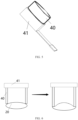
FIG. 5 is a schematic diagram of cooperation between a movable member and a driving member; and -
FIG. 6 is a schematic diagram of a liquid lens that deforms. -
- 10: screen substrate layer; 11: first packaging layer; 12: second packaging layer; 13: pixel;
- 20: liquid lens;
- 30: imaging sensor;
- 40: movable member; 41: driving member;
- 50: support layer; and
- 60: cover plate.
- The following clearly and completely describes technical solutions in embodiments of this application with reference to accompanying drawings in the embodiments of this application. Apparently, the described embodiments are some but not all of the embodiments of this application. All other embodiments obtained by a person of ordinary skill in the art based on the embodiments of this application without creative efforts shall fall within the protection scope of this application.
- The terms "first", "second", and the like in this specification and claims of this application are used to distinguish between similar objects instead of describing a specific order or sequence. It should be understood that the data used in such a way is interchangeable in proper circumstances so that the embodiments of this application can be implemented in an order other than the order illustrated or described herein. In addition, in this specification and the claims, "and/or" represents at least one of connected objects, and a character "/" generally represents an "or" relationship between associated objects.
- With reference to
FIG. 1 to FIG. 6 , an electronic device in an embodiment of this application is described in detail below based on specific embodiments and application scenarios thereof. - As shown in
FIG. 1 to FIG. 6 , the electronic device in this embodiment of this application includes ascreen substrate layer 10, aliquid lens 20, a driving structure, and animaging sensor 30. Thescreen substrate layer 10 may have a first region and a second region. The first region may be a light-transmitting region. For example, the first region may be a region made of a transparent material. Theliquid lens 20 is disposed in the first region, so that light can enter theliquid lens 20 conveniently. In addition, theliquid lens 20 may be in thescreen substrate layer 10, so that no hole needs to be formed, and an occupied space is small. This facilitates reducing an overall thickness and size. At least part of the first region is deformable. For example, the first region may deform under the action of an external force, so that deformation of the first region drives deformation of theliquid lens 20. Therefore, theliquid lens 20 can be focused. The driving structure may be disposed on a side of thescreen substrate layer 10. The driving structure may be configured to drive the first region to deform, thereby driving theliquid lens 20 to deform. Theimaging sensor 30 is disposed on a side of thescreen substrate layer 10. Theimaging sensor 30 may be disposed corresponding to theliquid lens 20. Therefore, light passing through theliquid lens 20 can form an image on theimaging sensor 30. No hole needs to be formed in the first region.Pixels 13 may be distributed in both the first region and the second region that are on the side of thescreen substrate layer 10 away from the driving structure. In other words, the pixels may be distributed on the entire surface of the side of thescreen substrate layer 10 away from the driving structure, thereby implementing full-screen display really. - In the electronic device in this embodiment of this application, the
liquid lens 20 is disposed in the first region that is light-transmitting. Theliquid lens 20 may be in thescreen substrate layer 10 and occupies a small space, so that an overall thickness can be reduced. The driving structure is configured to drive the first region to deform, thereby driving theliquid lens 20 to deform. A focal point can be determined fast based on a fine surface deformation that is generated after theliquid lens 20 is stressed, so that theliquid lens 20 can be focused fast, and the thickness of a module having a telephoto and macro function can be reduced greatly. No hole needs to be formed in the first region. Pixels may be distributed in both the first region and the second region that are on the side of thescreen substrate layer 10 away from the driving structure, so that full-screen display can be implemented really, and no hole needs to be formed in a screen. This facilitates increasing the light-sensing area of a camera and a pixel quantity. In addition, a night shooting capability can be improved without sacrificing an appearance, thereby improving a shooting effect. - In some embodiments, as shown in
FIG. 1 and FIG. 2 , the first region may include afirst packaging layer 11 and asecond packaging layer 12. Thefirst packaging layer 11 and thesecond packaging layer 12 may be disposed at an interval in a thickness direction of thescreen substrate layer 10. The thickness direction of thescreen substrate layer 10 is a direction perpendicular to theimaging sensor 30. Theliquid lens 20 is between thefirst packaging layer 11 and thesecond packaging layer 12. Thefirst packaging layer 11 and thesecond packaging layer 12 may be made of a transparent material. Theliquid lens 20 may be packaged by thefirst packaging layer 11 and thesecond packaging layer 12. Thefirst packaging layer 11 is deformable. The driving structure is configured to drive thefirst packaging layer 11 to deform. Deformation of thefirst packaging layer 11 may drive deformation of theliquid lens 20. Therefore, theliquid lens 20 can be focused fast. In an actual application process, thescreen substrate layer 10 may include a first substrate layer and a second substrate layer. Both the first substrate layer and the second substrate layer may be made of a transparent material. Theliquid lens 20 may be packaged between the first substrate layer and a second substrate layer. - In some other embodiments, the
second packaging layer 12 is also deformable. Deformation of thesecond packaging layer 12 may also drive theliquid lens 20 to deform. Therefore, theliquid lens 20 can be focused fast. - Pixels may be distributed in both the first region and the second region that are on the side of the
screen substrate layer 10 away from the driving structure, so that full-screen display can be implemented really, and no hole needs to be formed in a screen. This facilitates increasing the light-sensing area of a camera and a pixel quantity. In addition, a night shooting capability can be improved without sacrificing an appearance, thereby improving a shooting effect. - The
screen substrate layer 10 may be made of a transparent material. A position that is of thesecond packaging layer 12 and where theliquid lens 20 is packaged may be made of a material that cannot deform, for example, glass, polymethyl methacrylate (Polymethyl Methacrylate, PMMA), or the like. Thefirst packaging layer 11 may use a deformable material (for example, rubber). Theliquid lens 20 is packaged in thescreen substrate layer 10, so that a light-emitting pixel of the screen can be directly printed on a surface of the transparentsecond packaging layer 12, thereby implementing full-screen display. A focal length of theliquid lens 20 can be changed by controlling a deformation radian of thefirst packaging layer 11, thereby implementing a variation between macro and telephoto. - In this embodiment of this application, as shown in
FIG. 3 , a distribution density of the pixels in the first region of thescreen substrate layer 10 is less than a distribution density of the pixels in the second region of thescreen substrate layer 10. This can ensure the transmittance of the liquid lens, and reduce an impact on a display effect. - Optionally, as shown in
FIG. 4 , theimaging sensor 30 may be disposed on a side of thescreen substrate layer 10. Theimaging sensor 30 may be disposed corresponding to theliquid lens 20. Optical axes of theimaging sensor 30 and theliquid lens 20 may be collinear with each other, so that light entering theliquid lens 20 can form an image by using theimaging sensor 30. Theimaging sensor 30 that is configured to receive an optical signal may be connected to a central processing unit (Central Processing Unit, CPU) in a terminal through wiring. - In some embodiments, as shown in
FIG. 4 andFIG. 5 , the driving structure may include amovable member 40. Themovable member 40 may be disposed on a side of thescreen substrate layer 10. Themovable member 40 may extend along an edge of theliquid lens 20. Themovable member 40 is movable in a direction of the optical axis of theimaging sensor 30. In a case that themovable member 40 moves, themovable member 40 can drive theliquid lens 20 to deform. Theliquid lens 20 can be focused fast by using deformation of theliquid lens 20. For example, themovable member 40 may extend along the edge of theliquid lens 20 and stop at thefirst packaging layer 11 in a butting manner. In a case that themovable member 40 moves, themovable member 40 can drive thefirst packaging layer 11 to deform. Deformation of thefirst packaging layer 11 may drive deformation of theliquid lens 20. Therefore, theliquid lens 20 can be focused fast. - Optionally, the
movable member 40 may be circular, for example, a circular ring or a circular tube. An axis of themovable member 40 is parallel to or collinear with the optical axis of theimaging sensor 30. Therefore, theliquid lens 20 can deform stably to be focused fast. - In some embodiments, as shown in
FIG. 4 , theimaging sensor 30 may be disposed on a side of thescreen substrate layer 10. Theimaging sensor 30 may be disposed corresponding to theliquid lens 20. Themovable member 40 is between thescreen substrate layer 10 and theimaging sensor 30, so that light entering theliquid lens 20 can pass through themovable member 40, and then form an image by using theimaging sensor 30. - Optionally, the electronic device may further include a driving
member 41. The drivingmember 41 is configured to drive themovable member 40 to move in the direction of the optical axis of theimaging sensor 30. In a case that themovable member 40 moves, themovable member 40 can drive theliquid lens 20 to deform. Theliquid lens 20 can be focused fast by using deformation of theliquid lens 20. The drivingmember 41 may be a driving motor or a piezoelectric ceramic driving mechanism, or may be an electrostrictive material sheet. The electrostrictive material sheet may deform in a case that a voltage is exerted thereon. Deformation generated by the electrostrictive material sheet may drive themovable member 40 to move. - In an application process, a calculation formula of a focal length of the liquid lens may be as follows:

f denotes the focal length, d denotes a thickness of the liquid lens, r 1 and r 2 respectively denote curvature radii of two surfaces of the liquid lens, and n L denotes a refractive index of the liquid lens. - When the focal length is adjusted, a variation of the
liquid lens 20 may be shown inFIG. 6 . When the focal length is adjusted, the drivingmember 41 drives themovable member 40 to move. Themovable member 40 compresses a tensile surface of theliquid lens 20, making theliquid lens 20 deform. Therefore, curvatures of the two surfaces of theliquid lens 20 may vary, thereby implementing a variation of the focal length. A focal length after the compression and the deformation may be as follows:
f denotes the focal length, d denotes the thickness of the liquid lens, r 1 and r 2' respectively denote curvature radii of the two surfaces of the liquid lens after the deformation, and n L denotes the refractive index of the liquid lens. In a use process, the deformation of theliquid lens 20 may be adjusted based on an actual situation, so that theliquid lens 20 can reach a required focal length. - According to some embodiments, the electronic device may further include a
support layer 50. Thesupport layer 50 may be disposed on another side of thescreen substrate layer 10. Thesupport layer 50 may have a support function to ensure specific strength. Thesupport layer 50 may be adhered to the another side of thescreen substrate layer 10 by using an adhesive. For example, thesupport layer 50 is adhered to the another side of thescreen substrate layer 10 by using an optically clear adhesive. Theliquid lens 20 and thescreen substrate layer 10 may be directly packaged in thesupport layer 50. Thesupport layer 50 may also use a transparent material. - Optionally, the electronic device further includes a
cover plate 60. Thecover plate 60 may be disposed on the side of thesupport layer 50 away from thescreen substrate layer 10. Thecover plate 60 may be a glass plate, has a protective effect, and can ensure overall strength of a terminal, thereby further enhancing reliability. - In some embodiments, the
screen substrate layer 10 may be a transparent material member having high light transmittance, for example, a transparent plastic member. - The embodiments of this application are described above with reference to the accompanying drawings. However, this application is not limited to the foregoing specific implementations. The foregoing specific implementations are merely illustrative instead of restrictive. Under the enlightenment of this application, a person of ordinary skill in the art may make many forms without departing from the essence of this application and the protection scope of the claims, all of which fall within the protection of this application.
Claims (12)
- An electronic device, comprising:a screen substrate layer, wherein the screen substrate layer has a first region and a second region, and the first region is a light-transmitting region;a liquid lens, wherein the liquid lens is disposed in the first region, the liquid lens is in the screen substrate layer, and at least part of the first region is deformable;a driving structure, wherein the driving structure is disposed on a side of the screen substrate layer, and the driving structure is configured to drive the first region to deform, thereby driving the liquid lens to deform; andan imaging sensor, wherein the imaging sensor is disposed on a side of the screen substrate layer, and the imaging sensor is disposed corresponding to the liquid lens.
- The electronic device according to claim 1, wherein the first region comprises a first packaging layer and a second packaging layer, the first packaging layer and the second packaging layer are disposed at an interval in a thickness direction of the screen substrate layer, and the liquid lens is between the first packaging layer and the second packaging layer; and
the first packaging layer is deformable, the driving structure is configured to drive the first packaging layer to deform, and deformation of the first packaging layer is capable of driving the liquid lens to deform. - The electronic device according to claim 2, wherein the second packaging layer is deformable.
- The electronic device according to claim 1, wherein pixels are distributed in both the first region and the second region that are on the side of the screen substrate layer away from the driving structure.
- The electronic device according to claim 4, wherein a distribution density of the pixels in the first region of the screen substrate layer is less than a distribution density of the pixels in the second region of the screen substrate layer.
- The electronic device according to claim 1, wherein the driving structure comprises:
a movable member, wherein the movable member is disposed on a side of the screen substrate layer, the movable member extends along an edge of the liquid lens, the movable member is movable in a direction of an optical axis of the imaging sensor, and in a case that the movable member moves, the movable member is capable of driving the liquid lens to deform. - The electronic device according to claim 6, wherein the movable member is circular, and an axis of the movable member is parallel to or collinear with the optical axis of the imaging sensor.
- The electronic device according to claim 6, wherein the movable member is between the screen substrate layer and the imaging sensor.
- The electronic device according to claim 6, wherein the electronic device further comprises:
a driving member, wherein the driving member is configured to drive the movable member to move in the direction of the optical axis of the imaging sensor. - The electronic device according to claim 1, wherein the electronic device further comprises:
a support layer, wherein the support layer is disposed on another side of the screen substrate layer. - The electronic device according to claim 10, wherein the electronic device further comprises:
a cover plate, wherein the cover plate is disposed on the side of the support layer away from the screen substrate layer. - The electronic device according to claim 1, wherein the screen substrate layer is a transparent material member.
Applications Claiming Priority (2)
| Application Number | Priority Date | Filing Date | Title |
|---|---|---|---|
| CN202110976792.6A CN113691714B (en) | 2021-08-24 | 2021-08-24 | Electronic equipment |
| PCT/CN2022/113286 WO2023025029A1 (en) | 2021-08-24 | 2022-08-18 | Electronic device |
Publications (2)
| Publication Number | Publication Date |
|---|---|
| EP4394459A1 true EP4394459A1 (en) | 2024-07-03 |
| EP4394459A4 EP4394459A4 (en) | 2025-01-01 |
Family
ID=78582055
Family Applications (1)
| Application Number | Title | Priority Date | Filing Date |
|---|---|---|---|
| EP22860375.9A Pending EP4394459A4 (en) | 2021-08-24 | 2022-08-18 | ELECTRONIC DEVICE |
Country Status (4)
| Country | Link |
|---|---|
| US (1) | US20240192409A1 (en) |
| EP (1) | EP4394459A4 (en) |
| CN (1) | CN113691714B (en) |
| WO (1) | WO2023025029A1 (en) |
Families Citing this family (1)
| Publication number | Priority date | Publication date | Assignee | Title |
|---|---|---|---|---|
| CN113691714B (en) * | 2021-08-24 | 2023-07-25 | 维沃移动通信(杭州)有限公司 | Electronic equipment |
Family Cites Families (24)
| Publication number | Priority date | Publication date | Assignee | Title |
|---|---|---|---|---|
| JP2001133602A (en) * | 1999-11-10 | 2001-05-18 | Comoc:Kk | Micro lens array and display device using micro lens array |
| JP2001249202A (en) * | 2000-03-02 | 2001-09-14 | Japan Science & Technology Corp | Variable focus lens body and its control mechanism |
| DE602007006494D1 (en) * | 2006-08-01 | 2010-06-24 | Panasonic Corp | CAMERA DEVICE, LIQUID LENS AND IMAGE PROCESSING |
| JP2009047852A (en) * | 2007-08-17 | 2009-03-05 | Shinko Electric Ind Co Ltd | Image forming apparatus |
| JP2009175536A (en) * | 2008-01-25 | 2009-08-06 | Olympus Corp | Variable-focus liquid lens and method of manufacturing the same |
| CN100590475C (en) * | 2008-05-16 | 2010-02-17 | 东南大学 | A flexible liquid lens panel |
| CN101604035A (en) * | 2008-06-13 | 2009-12-16 | 鸿富锦精密工业(深圳)有限公司 | Liquid lens and lens module including the liquid lens |
| CN109073793B (en) * | 2018-07-06 | 2021-06-22 | 深圳市汇顶科技股份有限公司 | Liquid lens and processing method thereof and imaging module |
| JP7166824B2 (en) * | 2018-07-20 | 2022-11-08 | 株式会社ジャパンディスプレイ | Display device and electronic equipment incorporating the display device |
| CN109089024A (en) * | 2018-08-03 | 2018-12-25 | 信利光电股份有限公司 | It is a kind of can microshot camera module |
| CN111103922B (en) * | 2018-10-26 | 2023-08-25 | 华为技术有限公司 | Cameras, Electronic Devices and Authentication Methods |
| CN109254399B (en) * | 2018-11-02 | 2024-08-27 | 上海酷聚科技有限公司 | Display device and display method |
| EP4130836A3 (en) * | 2018-12-27 | 2023-05-24 | Tdk Taiwan Corp. | Optical system |
| US11586006B2 (en) * | 2018-12-27 | 2023-02-21 | Tdk Taiwan Corp. | Reflective element driving module |
| CN111505859A (en) * | 2019-01-31 | 2020-08-07 | 北京小米移动软件有限公司 | Liquid crystal display screen, display method and terminal |
| CN209674026U (en) * | 2019-03-14 | 2019-11-22 | 昆山龙腾光电有限公司 | A kind of capsule lens and display panel and display device containing capsule lens |
| JP7052765B2 (en) * | 2019-03-20 | 2022-04-12 | オムロン株式会社 | Image sensor |
| CN209928406U (en) * | 2019-03-28 | 2020-01-10 | 宁波舜宇光电信息有限公司 | Terminal equipment and display screen thereof |
| JP7295403B2 (en) * | 2019-05-22 | 2023-06-21 | ミツミ電機株式会社 | LENS DRIVING DEVICE, CAMERA MODULE, AND CAMERA MOUNTING DEVICE |
| CN110266861B (en) * | 2019-07-23 | 2022-04-19 | 京东方科技集团股份有限公司 | Display panel and display device |
| CN114223190A (en) * | 2019-09-29 | 2022-03-22 | Oppo广东移动通信有限公司 | Display screen, display assembly and electronic device |
| CN111308770A (en) * | 2020-02-26 | 2020-06-19 | 武汉华星光电技术有限公司 | Display device |
| CN113676579A (en) * | 2021-08-24 | 2021-11-19 | 维沃移动通信有限公司 | Electronic device |
| CN113691714B (en) * | 2021-08-24 | 2023-07-25 | 维沃移动通信(杭州)有限公司 | Electronic equipment |
-
2021
- 2021-08-24 CN CN202110976792.6A patent/CN113691714B/en active Active
-
2022
- 2022-08-18 EP EP22860375.9A patent/EP4394459A4/en active Pending
- 2022-08-18 WO PCT/CN2022/113286 patent/WO2023025029A1/en not_active Ceased
-
2024
- 2024-02-23 US US18/586,229 patent/US20240192409A1/en active Pending
Also Published As
| Publication number | Publication date |
|---|---|
| WO2023025029A1 (en) | 2023-03-02 |
| US20240192409A1 (en) | 2024-06-13 |
| EP4394459A4 (en) | 2025-01-01 |
| CN113691714B (en) | 2023-07-25 |
| CN113691714A (en) | 2021-11-23 |
Similar Documents
| Publication | Publication Date | Title |
|---|---|---|
| EP3819898B1 (en) | Display screen and terminal | |
| US20200234024A1 (en) | Under-screen fingerprint recognition system, liquid crystal display fingerprint recognition apparatus and electronic device | |
| CN210246879U (en) | Camera module and electronic equipment | |
| US20090310224A1 (en) | Liquid lens and lens module having same | |
| US10782508B2 (en) | Imaging apparatus including an optical assembly for refracting ambient lights to bypass shielding members in display panel and method for producing the same and mobile terminal device | |
| US9086761B2 (en) | Display apparatus | |
| KR20160119382A (en) | Display device | |
| CN111213080B (en) | Lenses, fingerprint recognition devices and electronic equipment | |
| CN117480437A (en) | Display modules and display devices | |
| CN109564338B (en) | Lens group, fingerprint recognition device and electronic equipment | |
| US20240192409A1 (en) | Electronic device | |
| EP1563331A1 (en) | Zoom lens | |
| EP4024272A1 (en) | Electronic device and control method thereof | |
| US12461279B2 (en) | Plastic light-folding element, imaging lens assembly module and electronic device | |
| CN115606193A (en) | Camera modules and electronic equipment | |
| CN107589617B (en) | A camera and mobile terminal | |
| CN110807417A (en) | Electronic equipment | |
| CN210807449U (en) | Camera module and electronic equipment | |
| KR20210060734A (en) | Electronic apparatus including the optical sensor and method of the manufacturing the same | |
| WO2023025018A1 (en) | Electronic device | |
| CN223078585U (en) | Backlight module, display module and display device | |
| CN112799212A (en) | Lens systems, optical sensing devices and electronics | |
| CN220509252U (en) | Electronic ink screen and electronic ink screen device | |
| TWI867590B (en) | Light path folding element, camera module and electronic device | |
| CN116320663A (en) | Camera module and electronic equipment |
Legal Events
| Date | Code | Title | Description |
|---|---|---|---|
| STAA | Information on the status of an ep patent application or granted ep patent |
Free format text: STATUS: THE INTERNATIONAL PUBLICATION HAS BEEN MADE |
|
| PUAI | Public reference made under article 153(3) epc to a published international application that has entered the european phase |
Free format text: ORIGINAL CODE: 0009012 |
|
| STAA | Information on the status of an ep patent application or granted ep patent |
Free format text: STATUS: REQUEST FOR EXAMINATION WAS MADE |
|
| 17P | Request for examination filed |
Effective date: 20240312 |
|
| AK | Designated contracting states |
Kind code of ref document: A1 Designated state(s): AL AT BE BG CH CY CZ DE DK EE ES FI FR GB GR HR HU IE IS IT LI LT LU LV MC MK MT NL NO PL PT RO RS SE SI SK SM TR |
|
| DAV | Request for validation of the european patent (deleted) | ||
| DAX | Request for extension of the european patent (deleted) | ||
| A4 | Supplementary search report drawn up and despatched |
Effective date: 20241128 |
|
| RIC1 | Information provided on ipc code assigned before grant |
Ipc: H04N 23/55 20230101ALI20241122BHEP Ipc: G02B 3/14 20060101AFI20241122BHEP |
|
| STAA | Information on the status of an ep patent application or granted ep patent |
Free format text: STATUS: EXAMINATION IS IN PROGRESS |
|
| 17Q | First examination report despatched |
Effective date: 20260303 |