EP4394093A1 - Nitride semiconductor substrate and method for producing same - Google Patents
Nitride semiconductor substrate and method for producing same Download PDFInfo
- Publication number
- EP4394093A1 EP4394093A1 EP22861137.2A EP22861137A EP4394093A1 EP 4394093 A1 EP4394093 A1 EP 4394093A1 EP 22861137 A EP22861137 A EP 22861137A EP 4394093 A1 EP4394093 A1 EP 4394093A1
- Authority
- EP
- European Patent Office
- Prior art keywords
- film
- substrate
- nitride semiconductor
- silicon
- semiconductor substrate
- Prior art date
- Legal status (The legal status is an assumption and is not a legal conclusion. Google has not performed a legal analysis and makes no representation as to the accuracy of the status listed.)
- Pending
Links
Images

Classifications
-
- C—CHEMISTRY; METALLURGY
- C30—CRYSTAL GROWTH
- C30B—SINGLE-CRYSTAL GROWTH; UNIDIRECTIONAL SOLIDIFICATION OF EUTECTIC MATERIAL OR UNIDIRECTIONAL DEMIXING OF EUTECTOID MATERIAL; REFINING BY ZONE-MELTING OF MATERIAL; PRODUCTION OF A HOMOGENEOUS POLYCRYSTALLINE MATERIAL WITH DEFINED STRUCTURE; SINGLE CRYSTALS OR HOMOGENEOUS POLYCRYSTALLINE MATERIAL WITH DEFINED STRUCTURE; AFTER-TREATMENT OF SINGLE CRYSTALS OR A HOMOGENEOUS POLYCRYSTALLINE MATERIAL WITH DEFINED STRUCTURE; APPARATUS THEREFOR
- C30B25/00—Single-crystal growth by chemical reaction of reactive gases, e.g. chemical vapour-deposition growth
- C30B25/02—Epitaxial-layer growth
-
- H—ELECTRICITY
- H10—SEMICONDUCTOR DEVICES; ELECTRIC SOLID-STATE DEVICES NOT OTHERWISE PROVIDED FOR
- H10P—GENERIC PROCESSES OR APPARATUS FOR THE MANUFACTURE OR TREATMENT OF DEVICES COVERED BY CLASS H10
- H10P14/00—Formation of materials, e.g. in the shape of layers or pillars
- H10P14/20—Formation of materials, e.g. in the shape of layers or pillars of semiconductor materials
- H10P14/34—Deposited materials, e.g. layers
- H10P14/3402—Deposited materials, e.g. layers characterised by the chemical composition
- H10P14/3414—Deposited materials, e.g. layers characterised by the chemical composition being group IIIA-VIA materials
- H10P14/3416—Nitrides
-
- C—CHEMISTRY; METALLURGY
- C30—CRYSTAL GROWTH
- C30B—SINGLE-CRYSTAL GROWTH; UNIDIRECTIONAL SOLIDIFICATION OF EUTECTIC MATERIAL OR UNIDIRECTIONAL DEMIXING OF EUTECTOID MATERIAL; REFINING BY ZONE-MELTING OF MATERIAL; PRODUCTION OF A HOMOGENEOUS POLYCRYSTALLINE MATERIAL WITH DEFINED STRUCTURE; SINGLE CRYSTALS OR HOMOGENEOUS POLYCRYSTALLINE MATERIAL WITH DEFINED STRUCTURE; AFTER-TREATMENT OF SINGLE CRYSTALS OR A HOMOGENEOUS POLYCRYSTALLINE MATERIAL WITH DEFINED STRUCTURE; APPARATUS THEREFOR
- C30B25/00—Single-crystal growth by chemical reaction of reactive gases, e.g. chemical vapour-deposition growth
- C30B25/02—Epitaxial-layer growth
- C30B25/18—Epitaxial-layer growth characterised by the substrate
- C30B25/183—Epitaxial-layer growth characterised by the substrate being provided with a buffer layer, e.g. a lattice matching layer
-
- C—CHEMISTRY; METALLURGY
- C30—CRYSTAL GROWTH
- C30B—SINGLE-CRYSTAL GROWTH; UNIDIRECTIONAL SOLIDIFICATION OF EUTECTIC MATERIAL OR UNIDIRECTIONAL DEMIXING OF EUTECTOID MATERIAL; REFINING BY ZONE-MELTING OF MATERIAL; PRODUCTION OF A HOMOGENEOUS POLYCRYSTALLINE MATERIAL WITH DEFINED STRUCTURE; SINGLE CRYSTALS OR HOMOGENEOUS POLYCRYSTALLINE MATERIAL WITH DEFINED STRUCTURE; AFTER-TREATMENT OF SINGLE CRYSTALS OR A HOMOGENEOUS POLYCRYSTALLINE MATERIAL WITH DEFINED STRUCTURE; APPARATUS THEREFOR
- C30B29/00—Single crystals or homogeneous polycrystalline material with defined structure characterised by the material or by their shape
- C30B29/10—Inorganic compounds or compositions
- C30B29/38—Nitrides
-
- C—CHEMISTRY; METALLURGY
- C30—CRYSTAL GROWTH
- C30B—SINGLE-CRYSTAL GROWTH; UNIDIRECTIONAL SOLIDIFICATION OF EUTECTIC MATERIAL OR UNIDIRECTIONAL DEMIXING OF EUTECTOID MATERIAL; REFINING BY ZONE-MELTING OF MATERIAL; PRODUCTION OF A HOMOGENEOUS POLYCRYSTALLINE MATERIAL WITH DEFINED STRUCTURE; SINGLE CRYSTALS OR HOMOGENEOUS POLYCRYSTALLINE MATERIAL WITH DEFINED STRUCTURE; AFTER-TREATMENT OF SINGLE CRYSTALS OR A HOMOGENEOUS POLYCRYSTALLINE MATERIAL WITH DEFINED STRUCTURE; APPARATUS THEREFOR
- C30B29/00—Single crystals or homogeneous polycrystalline material with defined structure characterised by the material or by their shape
- C30B29/10—Inorganic compounds or compositions
- C30B29/40—AIIIBV compounds wherein A is B, Al, Ga, In or Tl and B is N, P, As, Sb or Bi
- C30B29/403—AIII-nitrides
-
- C—CHEMISTRY; METALLURGY
- C30—CRYSTAL GROWTH
- C30B—SINGLE-CRYSTAL GROWTH; UNIDIRECTIONAL SOLIDIFICATION OF EUTECTIC MATERIAL OR UNIDIRECTIONAL DEMIXING OF EUTECTOID MATERIAL; REFINING BY ZONE-MELTING OF MATERIAL; PRODUCTION OF A HOMOGENEOUS POLYCRYSTALLINE MATERIAL WITH DEFINED STRUCTURE; SINGLE CRYSTALS OR HOMOGENEOUS POLYCRYSTALLINE MATERIAL WITH DEFINED STRUCTURE; AFTER-TREATMENT OF SINGLE CRYSTALS OR A HOMOGENEOUS POLYCRYSTALLINE MATERIAL WITH DEFINED STRUCTURE; APPARATUS THEREFOR
- C30B29/00—Single crystals or homogeneous polycrystalline material with defined structure characterised by the material or by their shape
- C30B29/10—Inorganic compounds or compositions
- C30B29/40—AIIIBV compounds wherein A is B, Al, Ga, In or Tl and B is N, P, As, Sb or Bi
- C30B29/403—AIII-nitrides
- C30B29/406—Gallium nitride
-
- H—ELECTRICITY
- H10—SEMICONDUCTOR DEVICES; ELECTRIC SOLID-STATE DEVICES NOT OTHERWISE PROVIDED FOR
- H10P—GENERIC PROCESSES OR APPARATUS FOR THE MANUFACTURE OR TREATMENT OF DEVICES COVERED BY CLASS H10
- H10P14/00—Formation of materials, e.g. in the shape of layers or pillars
- H10P14/20—Formation of materials, e.g. in the shape of layers or pillars of semiconductor materials
- H10P14/27—Formation of materials, e.g. in the shape of layers or pillars of semiconductor materials using selective deposition, e.g. simultaneous growth of monocrystalline and non-monocrystalline semiconductor materials
- H10P14/271—Formation of materials, e.g. in the shape of layers or pillars of semiconductor materials using selective deposition, e.g. simultaneous growth of monocrystalline and non-monocrystalline semiconductor materials characterised by the preparation of substrate for selective deposition
-
- H—ELECTRICITY
- H10—SEMICONDUCTOR DEVICES; ELECTRIC SOLID-STATE DEVICES NOT OTHERWISE PROVIDED FOR
- H10P—GENERIC PROCESSES OR APPARATUS FOR THE MANUFACTURE OR TREATMENT OF DEVICES COVERED BY CLASS H10
- H10P14/00—Formation of materials, e.g. in the shape of layers or pillars
- H10P14/20—Formation of materials, e.g. in the shape of layers or pillars of semiconductor materials
- H10P14/29—Formation of materials, e.g. in the shape of layers or pillars of semiconductor materials characterised by the substrates
- H10P14/2901—Materials
- H10P14/2902—Materials being Group IVA materials
- H10P14/2905—Silicon, silicon germanium or germanium
-
- H—ELECTRICITY
- H10—SEMICONDUCTOR DEVICES; ELECTRIC SOLID-STATE DEVICES NOT OTHERWISE PROVIDED FOR
- H10P—GENERIC PROCESSES OR APPARATUS FOR THE MANUFACTURE OR TREATMENT OF DEVICES COVERED BY CLASS H10
- H10P14/00—Formation of materials, e.g. in the shape of layers or pillars
- H10P14/20—Formation of materials, e.g. in the shape of layers or pillars of semiconductor materials
- H10P14/29—Formation of materials, e.g. in the shape of layers or pillars of semiconductor materials characterised by the substrates
- H10P14/2901—Materials
- H10P14/2907—Materials being Group IIIA-VA materials
- H10P14/2908—Nitrides
-
- H—ELECTRICITY
- H10—SEMICONDUCTOR DEVICES; ELECTRIC SOLID-STATE DEVICES NOT OTHERWISE PROVIDED FOR
- H10P—GENERIC PROCESSES OR APPARATUS FOR THE MANUFACTURE OR TREATMENT OF DEVICES COVERED BY CLASS H10
- H10P14/00—Formation of materials, e.g. in the shape of layers or pillars
- H10P14/20—Formation of materials, e.g. in the shape of layers or pillars of semiconductor materials
- H10P14/32—Formation of materials, e.g. in the shape of layers or pillars of semiconductor materials characterised by intermediate layers between substrates and deposited layers
- H10P14/3202—Materials thereof
- H10P14/3214—Materials thereof being Group IIIA-VA semiconductors
- H10P14/3216—Nitrides
-
- H—ELECTRICITY
- H10—SEMICONDUCTOR DEVICES; ELECTRIC SOLID-STATE DEVICES NOT OTHERWISE PROVIDED FOR
- H10P—GENERIC PROCESSES OR APPARATUS FOR THE MANUFACTURE OR TREATMENT OF DEVICES COVERED BY CLASS H10
- H10P14/00—Formation of materials, e.g. in the shape of layers or pillars
- H10P14/20—Formation of materials, e.g. in the shape of layers or pillars of semiconductor materials
- H10P14/24—Formation of materials, e.g. in the shape of layers or pillars of semiconductor materials using chemical vapour deposition [CVD]
Definitions
- the nitride semiconductor substrate has a single-crystallized nitride semiconductor thin film on the silicon nitride film, polycrystalline growth is prevented. Consequently, the residue of a chemical solution or the like does not remain during the process and does not cause a failure.
- a silicon oxide film was formed near the edge and on the edge portion, a nitride semiconductor composed of an AlN buffer layer, a buffer layer, and a GaN-HEMT structure was epitaxially grown as in Example.
- a nitride semiconductor composed of an AlN buffer layer, a buffer layer, and a GaN-HEMT structure was epitaxially grown as in Example.
- a polycrystal was grown on the silicon oxide film.
Landscapes
- Chemical & Material Sciences (AREA)
- Engineering & Computer Science (AREA)
- Crystallography & Structural Chemistry (AREA)
- Materials Engineering (AREA)
- Metallurgy (AREA)
- Organic Chemistry (AREA)
- Inorganic Chemistry (AREA)
- Chemical Kinetics & Catalysis (AREA)
- General Chemical & Material Sciences (AREA)
- Crystals, And After-Treatments Of Crystals (AREA)
- Recrystallisation Techniques (AREA)
- Junction Field-Effect Transistors (AREA)
Abstract
Description
- The present invention relates to a nitride semiconductor substrate and a method for manufacturing a nitride semiconductor substrate.
- Nitride semiconductors, including GaN and AlN, can be used for producing high electron mobility transistors (HEMT: High Electron Mobility Transistor) and electronic devices with a high breakdown voltage that use two-dimensional electron gas.
- It is difficult to produce a nitride wafer with these nitride semiconductor grown on a substrate. Thus, a sapphire substrate or a SiC substrate is used as the substrate. However, in order to achieve larger diameter and cost reduction of the substrate, epitaxial growth by vapor phase growth on a silicon substrate is employed (Patent Document 1). When an epitaxially grown film is formed by vapor phase growth on a silicon substrate, a substrate with a larger diameter can be used compared to the use of the sapphire substrate or the SiC substrate. Therefore, the productivity of devices is high, and there is an advantage in heat dissipation properties.
- When an AlN buffer layer, a buffer layer, and a GaN-HEMT structure is epitaxially grown on the silicon substrate, some part in the AlN buffer layer is not formed neatly near the edge. When a GaN layer or an AlGaN layer is laminated thereon, in the part where the AlN film is not formed, Ga in a raw material TMG reacts with Si to generate reaction marks. This reaction mark becomes a source of particle generation during a process. In addition, even if a SiO2 protective film is applied to prevent the generation of reaction marks, polycrystals grow on the protective film, and the residue of a chemical solution or the like remains during the process, causing failures. Consequently, it is necessary to eliminate the polycrystal growth part on a surface near the edge.
- Patent Document 1:
JP 2012-36030 A - The present invention has been made in view of the above-described problem. An object of the present invention is to provide a nitride semiconductor substrate without a reaction mark or a polycrystal growth portion on an edge portion when an AlN layer is epitaxially grown on a silicon substrate, and a nitride semiconductor thin film is epitaxially grown on top of that, and a method for manufacturing the nitride semiconductor substrate.
- To achieve the object, the present invention provides a nitride semiconductor substrate in which a nitride semiconductor thin film is formed on a substrate for film formation made of single-crystal silicon, wherein
a silicon nitride film is formed on a peripheral portion of the substrate for film formation; an AlN film is formed on the substrate for film formation and on the silicon nitride film; and the nitride semiconductor thin film is formed on the AlN film. - In this way, when the silicon nitride film is formed on the peripheral portion of the substrate for film formation made of single-crystal silicon, the generation of reaction mark is suppressed; thus, particles are not generated due to the reaction mark during a device process and adhesion of particles to the nitride semiconductor substrate is suppressed.
- In addition, the nitride semiconductor thin film on the silicon nitride film is preferably a single crystal.
- When the nitride semiconductor substrate has a single-crystallized nitride semiconductor thin film on the silicon nitride film, polycrystalline growth is prevented. Consequently, the residue of a chemical solution or the like does not remain during the process and does not cause a failure.
- Moreover, the present invention provides a method for manufacturing a nitride semiconductor substrate, the method comprising the steps of:
- (1) forming a silicon nitride film on a peripheral portion of a substrate for film formation made of single-crystal silicon;
- (2) growing an AlN film on the substrate for film formation and on the silicon nitride film on the peripheral portion; and
- (3) growing a GaN film, an AlGaN film, or both on the AlN film.
- With this manufacturing method, the nitride semiconductor substrate, without a reaction mark or a polycrystal growth portion on an edge portion, can be manufactured relatively easily and reliably.
- As described above, the present invention can provide a nitride semiconductor substrate and manufacturing method thereof without the reaction mark or polycrystalline growth part on the edge portion when a AlN layer is epitaxially grown on a silicon substrate and a nitride semiconductor thin film, especially a GaN or AlGaN layer, is epitaxially grown further on it.
-
-
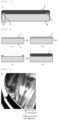
FIG. 1 is a schematic view illustrating an example of a nitride semiconductor substrate according to the present invention. -
FIG. 2 is a schematic view illustrating an example of a method for manufacturing a nitride semiconductor substrate according to the present invention. -
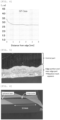
FIG. 3 is a photograph showing a part near an edge and an edge part of a nitride semiconductor substrate manufactured in Example. -
FIG. 4 is a graph showing the film thickness of the epitaxial layer measured at the edge and from the edge surface to the center in a nitride semiconductor substrate manufactured in Example. -
FIG. 5 is a photograph showing a part near an edge and an edge part of a nitride semiconductor substrate manufactured in Comparative Example 1. -
FIG. 6 is a cross-sectional photograph of a part near an edge and an edge part of a nitride semiconductor substrate manufactured in Comparative Example 2. -
FIG. 7 is an enlarged photograph showing the polycrystal part inFIG. 6 . - As described above, the development of a nitride semiconductor substrate is desired in which no reaction mark is generated on the edge portion when a nitride semiconductor composed of an AlN buffer layer, a buffer layer, and a GaN-HEMT structure is grown epitaxially on a silicon substrate.
- The present inventor has earnestly studied and found out that a silicon nitride film formed on the peripheral portion of a substrate for film formation made of single-crystal silicon can prevent the generation of a reaction mark, and that a polycrystal does not grow on the film, unlike a silicon oxide film. This finding has led to the completion of the present invention.
- That is, the present invention is a nitride semiconductor substrate in which a nitride semiconductor thin film is formed on a substrate for film formation made of single-crystal silicon, wherein
a silicon nitride film is formed on a peripheral portion of the substrate for film formation; an AlN film is formed on the substrate for film formation and on the silicon nitride film; and the nitride semiconductor thin film is formed on the AlN film. - Furthermore, the present invention is a method for manufacturing a nitride semiconductor substrate, the method comprising the steps of:
- (1) forming a silicon nitride film on a peripheral portion of a substrate for film formation made of single-crystal silicon;
- (2) growing an AlN film on the substrate for film formation and on the silicon nitride film on the peripheral portion; and
- (3) growing a GaN film, an AlGaN film, or both on the AlN film.
- Hereinafter, the present invention will be described in detail. However, the present invention is not limited thereto.
-
FIG. 1 shows a schematic view of an example of a nitride semiconductor substrate according to the present invention. The inventivenitride semiconductor substrate 1 has asilicon nitride film 3 formed on aperipheral portion 5 of asubstrate 2 for film formation made of single-crystal silicon; moreover, anepitaxial layer 4 formed on the center part of thesubstrate 2 for film formation, and on thesilicon nitride film 3 on theperipheral portion 5. Theepitaxial layer 4 includes an AlN film (buffer layer) formed on the center part of thesubstrate 2 for film formation and on thesilicon nitride film 3 on theperipheral portion 5 and a nitride semiconductor thin film formed on the AlN film. The nitride semiconductor thin film is not particularly limited but can be a GaN film, an AlGaN film, or both, for example. - At this point, the peripheral portion is, for example, an edge portion (the upper surface of the edge portion) and a region near the edge portion. The edge portion may be a chamfered surface.
- The film thickness of the
silicon nitride film 3 is not particularly limited, but, for example, can be 0.2 to 20 nm, preferably 1 to 4 nm, particularly 2 nm. The area of theperipheral portion 5 where thesilicon nitride film 3 is formed is not particularly limited, but, for example, can be the edge portion and the portion near the edge of 0.2 to 20 mm, preferably 0.5 to 10 mm, more preferably 1 to 5 mm, and particularly 2.5 mm. Moreover, the thickness of theepitaxial layer 4 is not particularly limited, but, for example, can be 0.1 to 20 um, preferably 0.5 to 10 µm, more preferably 1 to 5 µm, particularly about 2.7 µm. - The
substrate 2 for film formation made of single-crystal silicon is not particularly limited, but can be a CZ single-crystal silicon or an FZ single-crystal silicon and has no particular restriction on the presence or absence, type, and concentration of a dopant. - In the inventive nitride semiconductor substrate, since the silicon nitride film is formed on the peripheral portion of the substrate for film formation made of single-crystal silicon, the AlN film (buffer layer) is formed on the silicon nitride film on the peripheral portion of the growth substrate. Consequently, the AlN film (buffer layer) is well formed on the peripheral portion of the growth substrate; thus, when the GaN film or the AlGaN film is formed on the AlN film as the nitride semiconductor thin film, reaction marks cannot be generated by the reaction between Si in the growth substrate and Ga in the source gas. Moreover, by using the silicon nitride film as a film for coating the peripheral portion, the nitride semiconductor thin film formed thereon becomes a single crystal.
- The inventive nitride semiconductor substrate can be manufactured by an inventive method for manufacturing the nitride semiconductor substrate, as described below, for example. Hereinafter, referring to
FIG. 2 , the flow of the inventive method for manufacturing a nitride semiconductor substrate is described. - To begin with, a silicon nitride film is formed on the peripheral portion of a substrate for film formation made of single-crystal silicon (Step (1)).
- Firstly, as shown in
FIG. 2(a) , asubstrate 2 for film formation (silicon substrate) made of single-crystal silicon is placed into an RTA (Rapid Thermal Annealing) furnace and heat-treated in an ammonia atmosphere diluted with argon, for example, at 1175°C for 10 seconds or in a nitrogen atmosphere, for example, at 1200°C for 10 seconds to form asilicon nitride film 3 having a thickness of such as 2 nm on the surface of thesubstrate 2 for film formation. - Then, as shown in
FIG. 2(b) , a resist 6 is applied on thesilicon nitride film 3. - Then, as shown in
FIG. 2(c) , exposure and development are performed using the resist near the edge (for example, 2.5 mm) and on the edge portion as a protective film, and then the silicon substrate having the protective film near the edge and on the edge portion is etched, for example, for 10 seconds in a dry etching apparatus, thereby removing thesilicon nitride film 3 on the part having no protective film (the center part of thesubstrate 2 for film formation). Next, the resist protective film on the peripheral portion is removed and the substrate is cleaned. - Then, a step (step (2)) in which the AlN film is grown on the substrate for film formation, and on the silicon nitride film on the peripheral portion is performed, and a step (step (3)) in which a GaN film, an AlGaN film or both is grown on the AlN film is performed.
- As shown in
FIG. 2(d) , a nitride semiconductor (an epitaxial layer 4) including an AlN buffer layer, a buffer layer, and a GaN-HEMT layer is epitaxially grown in an MOCVD apparatus, for example, about 2.7 um. Thenitride semiconductor substrate 1 manufactured in this way has a single crystal grown also on the silicon nitride film on the peripheral portion without growing a polycrystal. In addition, no reaction mark is generated at the interface between the silicon nitride film and the silicon substrate. - Hereinafter, the present invention will be specifically described with Example and Comparative Examples. However, the present invention is not limited thereto.
- According to the flow in
FIG. 2 , a silicon substrate was placed in an RTA furnace, and heat-treated in an ammonia atmosphere diluted with argon at 1175°C for 10 seconds to form a silicon nitride film having a thickness of 2 nm on the entire surface. Photolithography was performed so that the resist film is left near the edge (2.5 mm) and on the edge portion. Then, etching was performed with a dry etching apparatus for 10 seconds to remove the silicon nitride film on the part having no resist film. After that, the resist film was removed and the substrate was cleaned, and a nitride semiconductor composed of an AlN buffer layer, a buffer layer, and a GaN-HEMT structure (total thickness of 2.7 µm) was epitaxially grown in an MOCVD apparatus. As a result, as shown in a photograph inFIG. 3 , it has been found that the wafer had a mirror plane near the edge and on the edge portion, having no reaction mark and no grown polycrystal. Furthermore,FIG. 4 shows the film thickness [um] of epitaxial growth: the epitaxial thickness was measured every 100 um with a cross sectional SEM on the edge portion and from the surface of the edge to the center. - Except that a silicon nitride film was not formed near the edge and on the edge portion, a nitride semiconductor composed of an AlN buffer layer, a buffer layer, and a GaN-HEMT structure was epitaxially grown on a silicon substrate as in Example. As a result, as shown in
FIG. 5 , a reaction mark was generated near the edge and on the edge portion of the wafer. - Except that a silicon oxide film was formed near the edge and on the edge portion, a nitride semiconductor composed of an AlN buffer layer, a buffer layer, and a GaN-HEMT structure was epitaxially grown as in Example. As a result, as shown in
FIG. 6 andFIG. 7 , although no reaction mark was observed near the edge and on the edge of the wafer, a polycrystal was grown on the silicon oxide film. - It should be noted that the present invention is not limited to the above-described embodiments. The embodiments are just examples, and any examples that have substantially the same feature and demonstrate the same functions and effects as those in the technical concept disclosed in claims of the present invention are included in the technical scope of the present invention.
Claims (3)
- A nitride semiconductor substrate in which a nitride semiconductor thin film is formed on a substrate for film formation made of single-crystal silicon, wherein
a silicon nitride film is formed on a peripheral portion of the substrate for film formation; an AlN film is formed on the substrate for film formation and on the silicon nitride film; and the nitride semiconductor thin film is formed on the AlN film. - The nitride semiconductor substrate according to claim 1, wherein
the nitride semiconductor thin film on the silicon nitride film is a single crystal. - A method for manufacturing a nitride semiconductor substrate, the method comprising the steps of:(1) forming a silicon nitride film on a peripheral portion of a substrate for film formation made of single-crystal silicon;(2) growing an AlN film on the substrate for film formation and on the silicon nitride film on the peripheral portion; and(3) growing a GaN film, an AlGaN film, or both on the AlN film.
Applications Claiming Priority (2)
| Application Number | Priority Date | Filing Date | Title |
|---|---|---|---|
| JP2021138308A JP7647446B2 (en) | 2021-08-26 | 2021-08-26 | Nitride semiconductor substrate and method for producing same |
| PCT/JP2022/030400 WO2023026847A1 (en) | 2021-08-26 | 2022-08-09 | Nitride semiconductor substrate and method for producing same |
Publications (2)
| Publication Number | Publication Date |
|---|---|
| EP4394093A1 true EP4394093A1 (en) | 2024-07-03 |
| EP4394093A4 EP4394093A4 (en) | 2025-08-06 |
Family
ID=85323145
Family Applications (1)
| Application Number | Title | Priority Date | Filing Date |
|---|---|---|---|
| EP22861137.2A Pending EP4394093A4 (en) | 2021-08-26 | 2022-08-09 | Nitride semiconductor substrate and method for producing the same |
Country Status (6)
| Country | Link |
|---|---|
| US (1) | US20240379352A1 (en) |
| EP (1) | EP4394093A4 (en) |
| JP (1) | JP7647446B2 (en) |
| CN (1) | CN117836477A (en) |
| TW (1) | TW202325919A (en) |
| WO (1) | WO2023026847A1 (en) |
Family Cites Families (4)
| Publication number | Priority date | Publication date | Assignee | Title |
|---|---|---|---|---|
| JP2009256154A (en) | 2008-04-21 | 2009-11-05 | Nippon Telegr & Teleph Corp <Ntt> | Substrate for growing semiconductor crystal and semiconductor crystal |
| JP2012036030A (en) * | 2010-08-05 | 2012-02-23 | Sanken Electric Co Ltd | Method for manufacturing semiconductor wafer |
| KR20130062736A (en) * | 2011-12-05 | 2013-06-13 | 삼성전자주식회사 | Silicon substrate, epitaxial structure having the same and manufacturing of silicon substrate |
| KR102188493B1 (en) * | 2014-04-25 | 2020-12-09 | 삼성전자주식회사 | Method of growing nitride single crystal and method of manufacturing nitride semiconductor device |
-
2021
- 2021-08-26 JP JP2021138308A patent/JP7647446B2/en active Active
-
2022
- 2022-08-09 US US18/683,703 patent/US20240379352A1/en active Pending
- 2022-08-09 EP EP22861137.2A patent/EP4394093A4/en active Pending
- 2022-08-09 CN CN202280056843.6A patent/CN117836477A/en active Pending
- 2022-08-09 WO PCT/JP2022/030400 patent/WO2023026847A1/en not_active Ceased
- 2022-08-12 TW TW111130382A patent/TW202325919A/en unknown
Also Published As
| Publication number | Publication date |
|---|---|
| EP4394093A4 (en) | 2025-08-06 |
| JP2023032276A (en) | 2023-03-09 |
| WO2023026847A1 (en) | 2023-03-02 |
| TW202325919A (en) | 2023-07-01 |
| US20240379352A1 (en) | 2024-11-14 |
| CN117836477A (en) | 2024-04-05 |
| JP7647446B2 (en) | 2025-03-18 |
Similar Documents
| Publication | Publication Date | Title |
|---|---|---|
| EP4012750A1 (en) | Substrate for electronic device and production method therefor | |
| CN101207174B (en) | Nitride semiconductor substrate and manufacturing method thereof | |
| CN100418191C (en) | epitaxial growth method | |
| EP2037013B1 (en) | Method for preparing substrate for growing gallium nitride and method for preparing gallium nitride substrate | |
| EP2538434A1 (en) | Epitaxial substrate and method for producing same | |
| US11705330B2 (en) | Substrate for electronic device and method for producing the same | |
| CN103682016A (en) | Manufacturing method for GaN epitaxy or substrate | |
| JP7068676B2 (en) | Non-etched gas-cooled epitaxial stack for group IIIA-N devices | |
| JP2009256154A (en) | Substrate for growing semiconductor crystal and semiconductor crystal | |
| KR20150007952A (en) | Method for manufacturing semiconductor device | |
| CN103959439B (en) | Semiconductor substrate and forming method | |
| CN101218662A (en) | Semiconductor substrate and masking layer for producing a free-standing semiconductor substrate by hydride vapor phase epitaxy and method for producing said free-standing semiconductor substrate | |
| US20130171811A1 (en) | Method for manufacturing compound semiconductor | |
| JP2004107114A (en) | Method of manufacturing group iii nitride compound semiconductor substrate | |
| US20240379352A1 (en) | Nitride semiconductor substrate and method for manufacturing the same | |
| CN101673670B (en) | A method for reducing the warpage of III-nitride self-supporting sheets | |
| EP4589057A1 (en) | Single crystal silicon substrate equipped with nitride semiconductor layer, and method for manufacturing single crystal silicon substrate equipped with nitride semiconductor layer | |
| EP4400636A1 (en) | Method for manufacturing nitride semiconductor substrate | |
| KR101635530B1 (en) | Method for the growth of nitride semiconductor crystal with voids and Method for the manufacturing of nitride semiconductor substrate thereof | |
| EP4492432A1 (en) | Group iii nitride semiconductor wafer, and manufacturing method thereof | |
| US8679953B1 (en) | Crystalline REO template on silicon substrate | |
| JP6983570B2 (en) | Manufacturing method of semiconductor laminate, manufacturing method of nitride semiconductor self-supporting substrate, semiconductor laminate and semiconductor device | |
| TWI752256B (en) | Substrate and method of making the same | |
| EP4723162A1 (en) | Method for manufacturing nitride semiconductor substrate, method for manufacturing hybrid ic, and nitride semiconductor substrate | |
| JP5667360B2 (en) | Semiconductor substrate, electronic device, and method for manufacturing semiconductor substrate |
Legal Events
| Date | Code | Title | Description |
|---|---|---|---|
| STAA | Information on the status of an ep patent application or granted ep patent |
Free format text: STATUS: THE INTERNATIONAL PUBLICATION HAS BEEN MADE |
|
| PUAI | Public reference made under article 153(3) epc to a published international application that has entered the european phase |
Free format text: ORIGINAL CODE: 0009012 |
|
| STAA | Information on the status of an ep patent application or granted ep patent |
Free format text: STATUS: REQUEST FOR EXAMINATION WAS MADE |
|
| 17P | Request for examination filed |
Effective date: 20240219 |
|
| AK | Designated contracting states |
Kind code of ref document: A1 Designated state(s): AL AT BE BG CH CY CZ DE DK EE ES FI FR GB GR HR HU IE IS IT LI LT LU LV MC MK MT NL NO PL PT RO RS SE SI SK SM TR |
|
| DAV | Request for validation of the european patent (deleted) | ||
| DAX | Request for extension of the european patent (deleted) | ||
| A4 | Supplementary search report drawn up and despatched |
Effective date: 20250707 |
|
| RIC1 | Information provided on ipc code assigned before grant |
Ipc: C30B 29/38 20060101AFI20250701BHEP Ipc: C30B 25/02 20060101ALI20250701BHEP Ipc: H01L 21/205 20060101ALI20250701BHEP Ipc: C30B 29/40 20060101ALI20250701BHEP |