EP4394064A1 - Lead-free free-cutting beryllium copper alloy - Google Patents
Lead-free free-cutting beryllium copper alloy Download PDFInfo
- Publication number
- EP4394064A1 EP4394064A1 EP23866641.6A EP23866641A EP4394064A1 EP 4394064 A1 EP4394064 A1 EP 4394064A1 EP 23866641 A EP23866641 A EP 23866641A EP 4394064 A1 EP4394064 A1 EP 4394064A1
- Authority
- EP
- European Patent Office
- Prior art keywords
- free
- copper alloy
- beryllium copper
- lead
- cutting
- Prior art date
- Legal status (The legal status is an assumption and is not a legal conclusion. Google has not performed a legal analysis and makes no representation as to the accuracy of the status listed.)
- Pending
Links
Images







Classifications
-
- C—CHEMISTRY; METALLURGY
- C22—METALLURGY; FERROUS OR NON-FERROUS ALLOYS; TREATMENT OF ALLOYS OR NON-FERROUS METALS
- C22C—ALLOYS
- C22C9/00—Alloys based on copper
-
- C—CHEMISTRY; METALLURGY
- C22—METALLURGY; FERROUS OR NON-FERROUS ALLOYS; TREATMENT OF ALLOYS OR NON-FERROUS METALS
- C22C—ALLOYS
- C22C9/00—Alloys based on copper
- C22C9/10—Alloys based on copper with silicon as the next major constituent
-
- C—CHEMISTRY; METALLURGY
- C22—METALLURGY; FERROUS OR NON-FERROUS ALLOYS; TREATMENT OF ALLOYS OR NON-FERROUS METALS
- C22F—CHANGING THE PHYSICAL STRUCTURE OF NON-FERROUS METALS AND NON-FERROUS ALLOYS
- C22F1/00—Changing the physical structure of non-ferrous metals or alloys by heat treatment or by hot or cold working
- C22F1/08—Changing the physical structure of non-ferrous metals or alloys by heat treatment or by hot or cold working of copper or alloys based thereon
Definitions
- the present invention relates to a lead-free free-cutting beryllium copper alloy.
- Patent Literature 1 JPS50-139017A discloses a quaternary copper alloy for spring materials, composed of from 0.5% to 1.5% of Be, from 0.2% to 3.0% of Sn, from 0.5% to 2.0% of Si, and the balance being Cu and inevitable impurities as an example of beryllium copper alloys.
- a free-cutting beryllium copper alloy (UNS No.: C17300) is generally known as a beryllium copper alloy with superior machinability. This alloy is improved in machinability by allowing beryllium copper to contain from about 0.2% to 0.6% by weight of lead (Pb).
- Patent Literature 2 JPS54-30369B discloses a free-cutting beryllium copper alloy as such a copper alloy, in which a copper alloy containing 0.5% to 4% by weight of Be is allowed to contain from 0.01% to 3% by weight of one selected from Pb, Te, and Bi, from 0.01% to 5% by weight of rare earth elements, and from 0.1% to 5% by weight of Al or Si.
- Patent Literature 3 JP2000-119775A discloses a leadless free-cutting copper alloy defined by an alloy composition composed of from 69% to 79% by weight of Cu, from 2.0% to 4.0% by weight of Si, and the balance consisting of Zn.
- Patent Literature 4 JP2021-42459A discloses a free-cutting copper alloy containing from 58.5 mass% to 63.5 mass% of Cu, from more than 0.4 mass% to 1.0 mass% of Si, from 0.003 mass% to 0.25 mass% of Pb, from 0.005 mass% to 0.19 mass% of P, and the balance composed of Zn and inevitable impurities.
- Lead-containing copper alloys including free-cutting beryllium copper alloys as disclosed in Patent Literature 2 are superior in machinability, as described above, and accordingly have been conventionally used as a constituent material of various products.
- lead is a harmful substance that adversely affects the human body and environment, and its use has tended to be greatly restricted in recent years.
- lead-free free-cutting brass has been developed, as disclosed in Patent Literatures 3 and 4.
- beryllium copper alloys however, there is no practical free-cutting material free from lead, and lead-free free-cutting beryllium copper alloys have been long awaited to be developed.
- an object of the present invention is to provide a lead-free free-cutting beryllium copper alloy that is superior in machinability.
- the present invention provides the following aspects:
- the lead-free free-cutting beryllium copper alloy according to the present invention consists of from 1.80% to 2.10% by weight of Be, from 0.10% to 3.00% by weight of Si, from 0.20% to 0.40% by weight of Co, from 0% to 0.10% by weight of Fe, from 0% to 0.10% by weight of Ni, and the balance being Cu and inevitable impurities.
- lead-free free-cutting beryllium copper alloy contains no lead (Pb).
- This copper alloy has a matrix phase being an ⁇ phase, a Si-rich phase being a ⁇ phase rich in Si, and Co-Be-Si intermetallic compound grains.
- the Co-Be-Si intermetallic compound grains contain Co, Be, and Si, and optionally Fe and/or Ni.
- a specific microstructure formed by allowing a beryllium copper alloy containing from 1.80% to 2.10% by weight of Be to contain from 0.10% to 3.00% by weight of Si can provide a lead-free beryllium copper alloy exhibiting superior machinability.
- Lead-containing copper alloys including free-cutting beryllium copper alloys, are superior in machinability, as described above, and accordingly have been conventionally used as a constituent material of various products.
- lead is a harmful substance that adversely affects the human body and environment, and its use has tended to be greatly restricted in recent years.
- the lead-free free-cutting beryllium copper alloy of the present invention can solve the above issue favorably. More specifically, allowing a beryllium copper alloy to contain Si reduces the cutting resistance of the beryllium copper alloy.
- the swarf produced by cutting beryllium copper alloys containing Si is easy to shear into chips and unlikely to wind around the tool.
- the beryllium copper alloy of the present invention exhibits superior machinability not only in terms of reducing cutting resistance but also in terms of improving the shapes of the swarf.
- "lead-free" in the lead-free free-cutting beryllium copper alloy means that the lead content is lower than or equal to the detection limit in the elemental analysis of the copper alloy.
- Si-rich phases and Co-Be-Si intermetallic compound grains containing Si probably serve as a stress concentration origin of shear failure to facilitate the braking of the swarf into smaller pieces.
- Be imparts superior fundamental performance (strength, workability, fatigue properties, heat resistance, corrosion resistance, etc.) as beryllium copper alloy to copper alloy.
- the Be content of the copper alloy of the present invention is from 1.80% to 2.10% by weight and is preferably from 1.80% to 2.00% by weight. A Be content in such a range can lead to the above-mentioned fundamental performance effectively and prevent excess Be from reducing electric conductivity.
- Si forms Si-rich phases and Co-Be-Si intermetallic compound grains to impart superior machinability to beryllium copper alloy.
- the Si content of the copper alloy of the present invention is from 0.10% to 3.00% by weight, preferably from 0.30% to 2.50% by weight, more preferably from 0.45% to 2.50% by weight, still more preferably from 0.50% to 2.20% by weight, particularly preferably from 0.80% to 2.00% by weight and is, for example, from 1.00% to 2.00% by weight.
- a Si content in such a range can improve machinability effectively and prevent excess Si from reducing productivity (causing cracking during forging) in actual operations.
- the Si content of the copper alloy can be preferably from 0.45% to 3.00% by weight, more preferably from 0.50% to 3.00% by weight, particularly preferably from 1.00% to 3.00% by weight, for example, from 2.00% to 3.00% by weight.
- Co forms Co-Be-Si intermetallic compound grains to impart superior machinability to beryllium copper alloy.
- the Co content of the copper alloy of the present invention is from 0.20% to 0.40% by weight, preferably from 0.20% to 0.35% by weight, more preferably from 0.22% to 0.30% by weight, and particularly preferably from 0.22% to 0.28% by weight.
- a Co content in such a range enables effective crystal refinement and the improvement of copper alloy properties and can prevent excess Co from reducing productivity in actual operations.
- Fe and Ni are optional elements that may be considered as impurities in the copper alloy of the present invention, and desired to be as little as possible because high Fe and Ni contents degrade mechanical properties. Accordingly, the Fe and Ni contents of the copper alloy of the present invention are each from 0% to 0.10% by weight, preferably from 0% to 0.005% by weight.
- the copper alloy of the present invention has a microstructure including a matrix phase, Si-rich phases, and Co-Be-Si intermetallic compound grains.
- the Si-rich phases are present in the matrix phase
- the Co-Be-Si intermetallic compound grains are present at the interfaces between the Si-rich phases and the matrix phase.
- the matrix phase is defined by an ⁇ phase and contributes to the superior fundamental performance (strength, workability, fatigue properties, heat resistance, corrosion resistance, etc.) as beryllium copper alloy.
- a Si-rich phase is defined by a ⁇ phase rich in Si and contributes to improving the machinability.
- the presence of Si in the matrix phase improves shearability and facilitates breaking the swarf into smaller pieces.
- the expression "rich in Si” means that Si is detected in a higher concentration in the elemental analysis than in the matrix phase ( ⁇ phase) and not necessarily in a higher concentration than in Co-Be-Si intermetallic compound grains.
- the matrix phase has a face-centered cubic (FCC) lattice crystal structure
- the Si-rich phase has a body-centered cubic (BCC) lattice crystal structure.
- the BCC structure is unlikely to deform and more shearable than the FCC structure. This means that Si-rich phases having a BCC structure can also contribute to improving the machinability.
- the percentage of area S BCC of BCC regions identified as body-centered cubic (BCC) lattices relative to the sum of area S FCC of FCC regions identified as face-centered cubic (FCC) lattices and area S BCC of BCC regions is preferably 5% or more, more preferably from 5 to 40%, still more preferably from 10 to 30%, particularly preferably from 15 to 30%, and most preferably from 15 to 25%.
- the EBSD measurement can be conducted according to the procedure and conditions described in the Examples below.
- Co-Be-Si intermetallic compound grains also contribute to improving the machinability.
- the Co-Be-Si intermetallic compound grains contain Co, Be, and Si, and optionally Fe and/or Ni.
- Co-Be-Si intermetallic compound grains contain Co, Be, and Si as essential elements, and these elements are dominant.
- Fe and Ni are optional elements or trace elements that can be considered impurities, as mentioned above and are, therefore, not considered dominant in the Co-Be-Si intermetallic compound grains.
- the Co-Be-Si intermetallic compound grains preferably have a hardness from 1.0 to 12.0 GPa, more preferably from 1.5 to 7.5 GPa, and still more preferably from 2.0 to 6.0 GPa as measured by a nanoindentation test in accordance with ISO14577. Having a hardness in such a range achieves machinability effectively.
- the nanoindentation test measures hardness in a small region at many points, and the resulting hardnesses have a wide distribution. Therefore, 100% of the measured points of the Co-Be-Si intermetallic compound grains need not be within the above ranges as long as the majority (for example, 90% or more) is within the above ranges. Hence, it is acceptable that the distribution of measured hardnesses includes hardnesses less than 1.0 GPa or higher than 12.0 GPa to a small extent (for example, less than 10%).
- the number of Co-Be-Si intermetallic compound grains is not limited, provided that the machinability of the beryllium copper alloy can be improved without impairing the above-described fundamental performance. From the viewpoint of improving machinability more effectively, the number of Co-Be-Si intermetallic compound grains at a cross section of the copper alloy is preferably 320 or less per unit area of 1 mm 2 , more preferably from 50 to 300, and still more preferably from 80 to 200.
- the shape of Co-Be-Si intermetallic compound grains is not limited to spherical and may be plate-like, rod-shaped, needle-shaped, or in variant shapes without limitation. Accordingly, the size of the Co-Be-Si intermetallic compound grains is preferably specified by cross-sectional area rather than by diameter.
- the Co-Be-Si intermetallic compound grains have a cross-sectional area preferably from 0.3 to 70 ⁇ m 2 per grain, more preferably from 1.0 to 65 ⁇ m 2 , and still more preferably from 5.0 to 60 ⁇ m 2 .
- the copper alloy of the present invention has superior machinability, as described above, and when a cross section of the swarf generated by cutting the copper alloy is observed along a longitudinal direction, the cross section of the swarf has a sheared profile with zigzag-shaped unevenness.
- the zigzag-shaped unevenness preferably satisfies the relationship 1.10 ⁇ h 2 /h 1 ⁇ 6.60, more preferably 2.0 ⁇ h 2 /h 1 ⁇ 6.6, and still more preferably 2.5 ⁇ h 2 /h 1 ⁇ 6.6, wherein as depicted in Figures 8 , h 1 represents the average of distances between recesses in the zigzag-shaped unevenness, and h 2 represents the average of heights of the protrusions in the unevenness.
- h 1 represents the average of distances between recesses in the zigzag-shaped unevenness
- h 2 represents the average of heights of the protrusions in the unevenness.
- the lead-free free-cutting beryllium copper alloy of the present invention can be preferably produced by, but not limited to, (a) melting and casting of raw materials for the above-described composition; (b) homogenization heat treatment; (c) hot working; (d) cold working; (e) solution annealing; and (f) aging treatment, in this order.
- the preferred aspects of copper alloys have been described above, and thus descriptions will be omitted here.
- one or more raw materials whose constituents are adjusted to result in the above-described composition are melted into a copper alloy molten metal. If a given element is added, the element alone, a master alloy, or the like can be added to the raw material. Alternatively, a raw material containing such additive elements may be melted together with a copper raw material.
- a copper alloy raw material that can provide the compositions presented in Table 1 was prepared.
- the copper alloy raw material was melted, and the resulting molten metal was poured into a mold to form a cylindrical ingot (billet).
- the resulting beryllium copper alloy sample (hereinafter referred to as a copper alloy sample) was evaluated in terms of the following.
- the hardness (GPa) of Co-Be-Si intermetallic compound grains at the cross section of beryllium copper alloys was measured at each microregion by a nanoindentation test. This test was performed in accordance with ISO14577 on samples with a Poisson's ratio of 0.3 under the conditions of 0.25 mN maximum load, 60 ⁇ m (X axis) ⁇ 60 ⁇ m (Y axis) measurement region, and 60 (X axis) ⁇ 60 (Y axis) measurement points using a nanoindenter (trade name: iMicro nanoindenter, manufactured by KLA Corporation). The hardness distribution of the Co-Be-Si intermetallic compound grains thus measured were represented by histograms.
- Copper alloy samples were used as work materials, and the cutting resistance (N) of the work materials when cut with a tool (tool bit) was examined. More specifically, a work material 2 was lowered while being rotated to be spirally cut with a tool 4, as depicted in Figure 10 under the test environment and cutting conditions below. At this time, the cutting resistance of the work material was measured with a multi-component force dynamometer (9129AA, manufactured by Kistler Group). The results are presented in Table 1.
Landscapes
- Chemical & Material Sciences (AREA)
- Engineering & Computer Science (AREA)
- Materials Engineering (AREA)
- Mechanical Engineering (AREA)
- Metallurgy (AREA)
- Organic Chemistry (AREA)
- Physics & Mathematics (AREA)
- Thermal Sciences (AREA)
- Crystallography & Structural Chemistry (AREA)
- Conductive Materials (AREA)
- Powder Metallurgy (AREA)
- Lead Frames For Integrated Circuits (AREA)
Abstract
Description
- The present invention relates to a lead-free free-cutting beryllium copper alloy.
- Beryllium copper alloys have traditionally been widely used in electronic components such as connectors because of their high strength and high electrical conductivity. Patent Literature 1 (
JPS50-139017A - Among beryllium copper alloys, a free-cutting beryllium copper alloy (UNS No.: C17300) is generally known as a beryllium copper alloy with superior machinability. This alloy is improved in machinability by allowing beryllium copper to contain from about 0.2% to 0.6% by weight of lead (Pb). For example, Patent Literature 2 (
JPS54-30369B - Also, free-cutting brass using brass materials has been developed, as well as beryllium copper alloys. For example, Patent Literature 3 (
JP2000-119775A JP2021-42459A -
- Patent Literature 1:
JPS50-139017A - Patent Literature 2:
JPS54-30369B - Patent Literature 3:
JP2000-119775A - Patent Literature 4:
JP2021-42459A - Lead-containing copper alloys, including free-cutting beryllium copper alloys as disclosed in
Patent Literature 2, are superior in machinability, as described above, and accordingly have been conventionally used as a constituent material of various products. However, lead is a harmful substance that adversely affects the human body and environment, and its use has tended to be greatly restricted in recent years. Accordingly, in brass materials, lead-free free-cutting brass has been developed, as disclosed inPatent Literatures - The present inventors have recently found that a specific microstructure formed by allowing a beryllium copper alloy containing from 1.80% to 2.10% by weight of Be to contain from 0.10% to 3.00% by weight of Si can provide a lead-free beryllium copper alloy exhibiting superior machinability.
- Accordingly, an object of the present invention is to provide a lead-free free-cutting beryllium copper alloy that is superior in machinability.
- The present invention provides the following aspects:
- [Aspect 1]
A lead-free free-cutting beryllium copper alloy, consisting of:- from 1.80% to 2.10% by weight of Be;
- from 0.10% to 3.00% by weight of Si;
- from 0.20% to 0.40% by weight of Co;
- from 0% to 0.10% by weight of Fe;
- from 0% to 0.10% by weight of Ni; and
- the balance being Cu and inevitable impurities,
- wherein the beryllium copper alloy has:
- a matrix phase being an α phase,
- a Si-rich phase being a κ phase rich in Si, and
- Co-Be-Si intermetallic compound grains containing Co, Be, and Si, and optionally Fe and/or Ni.
- [Aspect 2] The lead-free free-cutting beryllium copper alloy according to aspect 1, wherein the Co-Be-Si intermetallic compound grains exhibit a hardness from 1.0 to 12.0 GPa as measured by a nanoindentation test in accordance with ISO14577.
- [Aspect 3] The lead-free free-cutting beryllium copper alloy according to
aspect 1 or 2, wherein the number of the Co-Be-Si intermetallic compound grains present at a cross section of the lead-free free-cutting beryllium copper alloy is 320 or less per unit area of 1 mm2. - [Aspect 4] The lead-free free-cutting beryllium copper alloy according to any one of aspects 1 to 3, wherein when a cross section of the lead-free free-cutting beryllium copper alloy is observed, the Co-Be-Si intermetallic compound grains have a cross-sectional area from 0.3 to 70 µm2 per grain.
- [Aspect 5] The lead-free free-cutting beryllium copper alloy according to any one of aspects 1 to 4, wherein when a cross section of swarf generated by cutting the lead-free free-cutting beryllium copper alloy is observed along a longitudinal direction, the cross section of the swarf has a sheared profile with zigzag-shaped unevenness that satisfies a relationship 1.10 < h2/h1 < 6.60, wherein h1 represents the average of distances between recesses in the zigzag-shaped unevenness, and h2 represents the average of heights of protrusions in the unevenness.
- [Aspect 6] The lead-free free-cutting beryllium copper alloy according to any one of aspects 1 to 5, wherein in a phase map of 75 µm × 75 µm field of view obtained by electron beam backscatter diffraction (EBSD) analysis of a cross section of the lead-free free-cutting beryllium copper alloy, the percentage of area SBCC of BCC regions identified as body-centered cubic (BCC) lattices relative to the sum of area SFCC of FCC regions identified as face-centered cubic (FCC) lattices and area SBCC, that is, 100 × SBCC/(SFCC + SBCC), is 5% or more.
-
-
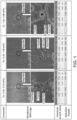
Figure 1 depicts sectional SEM images and SEM-EDX results of copper alloy samples of Examples 4, 6, and 7. -
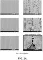
Figure 2A depicts sectional SEM images of the copper alloy sample (Si: 1.09% by weight) of Example 6 at varying magnifications. -
Figure 2B depicts EPMA mapping images of Example 6 measured in the region corresponding to the SEM image in the lower right ofFigure 2A . -
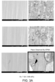
Figure 3A depicts sectional SEM images of the copper alloy sample (Si: 2.98% by weight) of Example 7 at varying magnifications. -
Figure 3B depicts EPMA mapping images of Example 7 measured in the region corresponding to the SEM image in the lower right ofFigure 3A . -
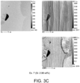
Figure 3C depicts EPMA mapping images of Example 7 measured in the region corresponding to the SEM image in the lower right ofFigure 3A . -
Figure 4A depicts sectional STEM images of the copper alloy sample (Si: 1.09% by weight) of Example 6 at varying magnifications. -
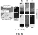
Figure 4B depicts STEM-EELS mapping images of Example 6 measured in the region corresponding to the STEM image at the right end ofFigure 4A . -
Figure 5A depicts a CCD image of the copper alloy sample (Si: 0.29% by weight) of Example 4 and the hardness distribution in the rectangular region of the CCD image. -
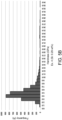
Figure 5B depicts a histogram of the hardness distribution of intermetallic compound grains measured for the copper alloy sample (Si: 0.29% by weight) of Example 4. -
Figure 6 depicts a sectional SEM image of the copper alloy sample (Si: 2.98% by weight) of Example 7. -
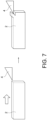
Figure 7 depicts schematic diagrams illustrating the method of cutting a copper alloy sample in machinability evaluation 1 for the Examples. -
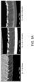
Figure 8A depicts SEM images in observing cross sections of swarf from copper alloy samples in Examples 2 to 4. -
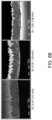
Figure 8B depicts SEM images in observing cross sections of swarf from copper alloy samples in Examples 5 to 7. -
Figure 9 depicts a schematic diagram illustrating distance h1 between recesses and the largest height h2 of the protrusions in the unevenness at a cross section of swarf in machinability evaluation 1 for the Examples. -
Figure 10 depicts a schematic diagram illustrating the method of cutting a copper alloy sample inmachinability evaluation 2 for the Examples. -
Figure 11 depicts Table 2 presenting sectional SEM images of copper alloy samples of Examples 1 and 5 to 7 and EBSD phase maps of the regions corresponding to the respective sectional SEM images, each together with the area percentage of the BCC region and the cutting resistance (thrust force). - The lead-free free-cutting beryllium copper alloy according to the present invention consists of from 1.80% to 2.10% by weight of Be, from 0.10% to 3.00% by weight of Si, from 0.20% to 0.40% by weight of Co, from 0% to 0.10% by weight of Fe, from 0% to 0.10% by weight of Ni, and the balance being Cu and inevitable impurities. Needless to say, lead-free free-cutting beryllium copper alloy contains no lead (Pb). This copper alloy has a matrix phase being an α phase, a Si-rich phase being a κ phase rich in Si, and Co-Be-Si intermetallic compound grains. The Co-Be-Si intermetallic compound grains contain Co, Be, and Si, and optionally Fe and/or Ni. Thus, a specific microstructure formed by allowing a beryllium copper alloy containing from 1.80% to 2.10% by weight of Be to contain from 0.10% to 3.00% by weight of Si can provide a lead-free beryllium copper alloy exhibiting superior machinability.
- Lead-containing copper alloys, including free-cutting beryllium copper alloys, are superior in machinability, as described above, and accordingly have been conventionally used as a constituent material of various products. However, lead is a harmful substance that adversely affects the human body and environment, and its use has tended to be greatly restricted in recent years. For beryllium copper alloys, it is an issue that there is no practical lead-free free-cutting material. In this regard, the lead-free free-cutting beryllium copper alloy of the present invention can solve the above issue favorably. More specifically, allowing a beryllium copper alloy to contain Si reduces the cutting resistance of the beryllium copper alloy. Also, the swarf produced by cutting beryllium copper alloys containing Si is easy to shear into chips and unlikely to wind around the tool. Thus, the beryllium copper alloy of the present invention exhibits superior machinability not only in terms of reducing cutting resistance but also in terms of improving the shapes of the swarf. Note that "lead-free" in the lead-free free-cutting beryllium copper alloy means that the lead content is lower than or equal to the detection limit in the elemental analysis of the copper alloy.
- Although the mechanism by which the presence of Si (particularly, the presence of Si-rich phases and Co-Be-Si intermetallic compound grains) improves the machinability is not clear, the Si-rich phases and Co-Be-Si intermetallic compound grains containing Si probably serve as a stress concentration origin of shear failure to facilitate the braking of the swarf into smaller pieces.
- Be imparts superior fundamental performance (strength, workability, fatigue properties, heat resistance, corrosion resistance, etc.) as beryllium copper alloy to copper alloy. The Be content of the copper alloy of the present invention is from 1.80% to 2.10% by weight and is preferably from 1.80% to 2.00% by weight. A Be content in such a range can lead to the above-mentioned fundamental performance effectively and prevent excess Be from reducing electric conductivity.
- Si forms Si-rich phases and Co-Be-Si intermetallic compound grains to impart superior machinability to beryllium copper alloy. The Si content of the copper alloy of the present invention is from 0.10% to 3.00% by weight, preferably from 0.30% to 2.50% by weight, more preferably from 0.45% to 2.50% by weight, still more preferably from 0.50% to 2.20% by weight, particularly preferably from 0.80% to 2.00% by weight and is, for example, from 1.00% to 2.00% by weight. A Si content in such a range can improve machinability effectively and prevent excess Si from reducing productivity (causing cracking during forging) in actual operations. Particularly when the Si content is 0.45% by weight or more, Si-rich phases increase with statistical significance, and their remarkable shear occurs during cutting, further improving machinability. Accordingly, the Si content of the copper alloy can be preferably from 0.45% to 3.00% by weight, more preferably from 0.50% to 3.00% by weight, particularly preferably from 1.00% to 3.00% by weight, for example, from 2.00% to 3.00% by weight.
- Co forms Co-Be-Si intermetallic compound grains to impart superior machinability to beryllium copper alloy. The Co content of the copper alloy of the present invention is from 0.20% to 0.40% by weight, preferably from 0.20% to 0.35% by weight, more preferably from 0.22% to 0.30% by weight, and particularly preferably from 0.22% to 0.28% by weight. A Co content in such a range enables effective crystal refinement and the improvement of copper alloy properties and can prevent excess Co from reducing productivity in actual operations.
- Fe and Ni are optional elements that may be considered as impurities in the copper alloy of the present invention, and desired to be as little as possible because high Fe and Ni contents degrade mechanical properties. Accordingly, the Fe and Ni contents of the copper alloy of the present invention are each from 0% to 0.10% by weight, preferably from 0% to 0.005% by weight.
- As described above, the copper alloy of the present invention has a microstructure including a matrix phase, Si-rich phases, and Co-Be-Si intermetallic compound grains. Typically, the Si-rich phases are present in the matrix phase, and the Co-Be-Si intermetallic compound grains are present at the interfaces between the Si-rich phases and the matrix phase.
- The matrix phase is defined by an α phase and contributes to the superior fundamental performance (strength, workability, fatigue properties, heat resistance, corrosion resistance, etc.) as beryllium copper alloy.
- A Si-rich phase is defined by a κ phase rich in Si and contributes to improving the machinability. In particular, the presence of Si in the matrix phase improves shearability and facilitates breaking the swarf into smaller pieces. The expression "rich in Si" means that Si is detected in a higher concentration in the elemental analysis than in the matrix phase (α phase) and not necessarily in a higher concentration than in Co-Be-Si intermetallic compound grains.
- Typically, the matrix phase has a face-centered cubic (FCC) lattice crystal structure, while the Si-rich phase has a body-centered cubic (BCC) lattice crystal structure. The BCC structure is unlikely to deform and more shearable than the FCC structure. This means that Si-rich phases having a BCC structure can also contribute to improving the machinability. Accordingly, in a phase map of 75 µm × 75 µm field of view obtained by electron beam backscatter diffraction (EBSD) analysis of a cross section of the beryllium copper alloy, the percentage of area SBCC of BCC regions identified as body-centered cubic (BCC) lattices relative to the sum of area SFCC of FCC regions identified as face-centered cubic (FCC) lattices and area SBCC of BCC regions (that is, 100 × SBCC / (SFCC + SBCC)) is preferably 5% or more, more preferably from 5 to 40%, still more preferably from 10 to 30%, particularly preferably from 15 to 30%, and most preferably from 15 to 25%. By increasing the percentage of such a BCC structure, the cutting resistance (particularly thrust force) can be reduced, resulting in further improved machinability. The EBSD measurement can be conducted according to the procedure and conditions described in the Examples below.
- Co-Be-Si intermetallic compound grains also contribute to improving the machinability. The Co-Be-Si intermetallic compound grains contain Co, Be, and Si, and optionally Fe and/or Ni. Hence, Co-Be-Si intermetallic compound grains contain Co, Be, and Si as essential elements, and these elements are dominant. Fe and Ni are optional elements or trace elements that can be considered impurities, as mentioned above and are, therefore, not considered dominant in the Co-Be-Si intermetallic compound grains.
- The Co-Be-Si intermetallic compound grains preferably have a hardness from 1.0 to 12.0 GPa, more preferably from 1.5 to 7.5 GPa, and still more preferably from 2.0 to 6.0 GPa as measured by a nanoindentation test in accordance with ISO14577. Having a hardness in such a range achieves machinability effectively. The nanoindentation test measures hardness in a small region at many points, and the resulting hardnesses have a wide distribution. Therefore, 100% of the measured points of the Co-Be-Si intermetallic compound grains need not be within the above ranges as long as the majority (for example, 90% or more) is within the above ranges. Hence, it is acceptable that the distribution of measured hardnesses includes hardnesses less than 1.0 GPa or higher than 12.0 GPa to a small extent (for example, less than 10%).
- The number of Co-Be-Si intermetallic compound grains is not limited, provided that the machinability of the beryllium copper alloy can be improved without impairing the above-described fundamental performance. From the viewpoint of improving machinability more effectively, the number of Co-Be-Si intermetallic compound grains at a cross section of the copper alloy is preferably 320 or less per unit area of 1 mm2, more preferably from 50 to 300, and still more preferably from 80 to 200.
- The shape of Co-Be-Si intermetallic compound grains is not limited to spherical and may be plate-like, rod-shaped, needle-shaped, or in variant shapes without limitation. Accordingly, the size of the Co-Be-Si intermetallic compound grains is preferably specified by cross-sectional area rather than by diameter. For example, in the cross section of the beryllium copper alloy, the Co-Be-Si intermetallic compound grains have a cross-sectional area preferably from 0.3 to 70 µm2 per grain, more preferably from 1.0 to 65 µm2, and still more preferably from 5.0 to 60 µm2.
- The copper alloy of the present invention has superior machinability, as described above, and when a cross section of the swarf generated by cutting the copper alloy is observed along a longitudinal direction, the cross section of the swarf has a sheared profile with zigzag-shaped unevenness. In this instance, the zigzag-shaped unevenness preferably satisfies the relationship 1.10 < h2/h1 < 6.60, more preferably 2.0 < h2/h1 < 6.6, and still more preferably 2.5 < h2/h1 <6.6, wherein as depicted in
Figures 8 , h1 represents the average of distances between recesses in the zigzag-shaped unevenness, and h2 represents the average of heights of the protrusions in the unevenness. When the swarf produced by cutting the copper alloy has such a sheared profile, the swarf is easy to shear into chips and unlikely to wind around the tool. Such copper alloy can be superior in machinability. In contrast, when the swarf has an undulatory profile (smoothly uneven profile) rather than a sheared profile, the swarf easily forms strings of cut pieces, which are likely to wind around the tool, reducing productivity. - The lead-free free-cutting beryllium copper alloy of the present invention can be preferably produced by, but not limited to, (a) melting and casting of raw materials for the above-described composition; (b) homogenization heat treatment; (c) hot working; (d) cold working; (e) solution annealing; and (f) aging treatment, in this order. The preferred aspects of copper alloys have been described above, and thus descriptions will be omitted here.
- First, one or more raw materials whose constituents are adjusted to result in the above-described composition (that is, composition consisting of from 1.80% to 2.10% by weight of Be, from 0.10% to 3.00% by weight of Si, from 0.20% to 0.40% by weight of Co, from 0% to 0.10% by weight of Fe, from 0% to 0.10% by weight of Ni, and the balance being Cu and inevitable impurities) are melted into a copper alloy molten metal. If a given element is added, the element alone, a master alloy, or the like can be added to the raw material. Alternatively, a raw material containing such additive elements may be melted together with a copper raw material. Then, the copper alloy molten metal whose constituents are adjusted to result in the above-described composition is poured into a mold to form an ingot. For mass production, continuous casting is preferred. Thus, a (cylindrical, for example) ingot (billet) can be produced.
- The resulting ingot is subjected to homogenization heat treatment. That is, the ingot is homogenized by heating. In homogenization heat treatment, the heating temperature of the ingot is preferably in the range of 500 to 900°C, and the temperature is preferably held in this range for a period from 1 to 24 hours.
- The ingot subjected to homogenization heat treatment is hot-worked into a hot-worked material with a predetermined diameter. Before hot working, the homogenized ingot may be optionally annealed for softening to improve workability. Although, at this time, annealing conditions are not limited, the heating temperature is preferably in the range from 500 to 900°C, and the temperature is preferably held in this range for a period from 0.2 to 6 hours.
- The resulting hot-worked material is cold-worked into a cold-worked material with a predetermined diameter. The cold working percentage is preferably from 0.5 to 95%. Before cold working, the hot-worked material may be optionally annealed for softening to improve workability. Although, at this time, annealing conditions are not limited, the heating temperature is preferably in the range from 500 to 900°C, and the temperature is preferably held in this range for a period from 0.2 to 6 hours.
- The resulting cold-worked material is subjected to solution annealing to uniformly dissolve the elements in the material, yielding a solution-annealed material. In the solution annealing, the solution annealing temperature is preferably in the range from 600 to 900°C, and the temperature is preferably held in this range for a period from 0.2 to 3 hours.
- The resulting solution-annealed material is subjected to aging treatment to obtain the beryllium copper alloy of the present invention. In the aging treatment, the aging temperature is preferably in the range from 200 to 500°C, and the temperature is preferably held in this range for a period from 0.2 to 3 hours. Before aging treatment, the solution-annealed material may be optionally subjected to cold working or oxide coating removal. At this time, the cold working conditions are not limited, but the working percentage is preferably from 0.5 to 95%.
- The lead-free beryllium copper alloy with superior machinability can be favorably produced through the above steps (a) to (f).
- The present invention will be further described in detail with reference to the following Examples.
- Beryllium copper alloys were produced according to the following procedure and evaluated.
- First, a copper alloy raw material that can provide the compositions presented in Table 1 was prepared. The copper alloy raw material was melted, and the resulting molten metal was poured into a mold to form a cylindrical ingot (billet).
- The resulting ingot was held at 800°C for 4 hours for homogenization heat treatment.
- The ingot subjected to homogenization heat treatment was annealed at 800°C for 1 hour and then hot-worked into a cylindrical hot-worked material with a diameter of 1.8 cm.
- Before hot-working into a hot-worked material, the material was annealed at 800°C for 1 hour and then subjected to cold-working at a working percentage of 40% into a cylindrical cold-worked material with a diameter of 1.4 cm.
- The resulting cold-worked material was subjected to solution annealing at 800°C for 1 hour to yield a solution-annealed material.
- The solution-annealed material was cold-worked at a working percentage of 38%. The resulting solution-annealed material was subjected to aging treatment at 320°C for 2 hours to yield a cylindrical beryllium copper alloy sample with a diameter of 1.1 cm and a length of 100 cm.
- The resulting beryllium copper alloy sample (hereinafter referred to as a copper alloy sample) was evaluated in terms of the following.
- The copper alloy sample was cut into a cross section and sliced with a focused ion beam (FIB). The resulting cross section was observed under an SEM (scanning electron microscope), and the cross section was subjected to elemental analysis under the measurement condition of an accelerating voltage of 15 kV with an energy dispersive X-ray analyzer (EDX, model name: JXA-8530FPlus, manufactured by JEOL Ltd.) attached to the SEM. The same cross section was also subjected to elemental analysis under the measurement condition of an accelerating voltage of 15 kV with an electron probe microanalyzer (EPMA, model name: JXA-8530FPlus, manufactured by JEOL Ltd.)
- The results showed that the beryllium copper alloys of Examples 3 to 7 include the matrix phase, Si-rich phases containing a higher concentration of Si than the matrix phase, and Co-Be-Si intermetallic compound grains containing Co, Be, Si, Fe, and Ni. It was also identified that Co-Be-Si intermetallic compound grains contain a still higher concentration of Si than the Si-rich phases.
Figure 1 depicts SEM images of the samples of Examples 4, 6, and 7 and their SEM-EDX results at individual measurementlocations. -
Figure 2A depicts sectional SEM images of the copper alloy sample (Si: 1.09% by weight) of Example 6 at varying magnifications. InFigure 2A , the three SEM images on the left are secondary electron micrographs, clearly showing fine structures at a surface of the sample, and the three SEM images on the right are backscattered electron composition images (COMPO images), showing contrasts dependent on the atomic numbers. Any of these six SEM images are obtained by observing the same face of the sample.Figure 2B depicts EPMA mapping images of Example 6 measured in the region corresponding to the SEM image in the lower right ofFigure 2A . - Similarly,
Figure 3A depicts sectional SEM images of the copper alloy sample (Si: 2.98% by weight) of Example 7 at varying magnifications. InFigure 3A , the three SEM images on the left are secondary electron micrographs, clearly showing fine structures at a surface of the sample, and the three SEM images on the right are backscattered electron composition images (COMPO images), showing contrasts dependent on the atomic numbers. Any of these six SEM images are obtained by observing the same face of the sample.Figures 3B and3C depict EPMA mapping images of Example 7 measured in the region corresponding to the SEM image in the lower right ofFigure 3A . - The copper alloy sample was cut into a cross section and sliced with a focused ion beam (FIB). The resulting cross section was observed under the measurement condition at an accelerating voltage of 200 kV under a scanning transmission electron microscope with a spherical aberration correction function (STEM, model name: HD-2700, manufactured by Hitachi High-Tech Corporation). Additionally, elemental analysis was performed on the vicinity of interfaces between the matrix phase and the intermetallic compound grains under the measurement condition of 200 kV voltage with an electron energy loss spectrometer (EELS, trade name: Enfinium, manufactured by Gatan Inc.) / energy dispersive X-ray analyzer (EDX, model name: XMAXN 100TLE, manufactured by Oxford Instruments plc) attached to the STEM. The results showed that the intermetallic compound grains in the beryllium copper alloys of Examples 3 to 7 were dominated by Co, Be, and Si, with Ni and Fe merely in trace amounts. Hence, the presence of Co-Be-Si intermetallic compound grains was confirmed. Also, it was identified that the matrix phase contains mainly Be and Cu, in which Cu is dominant. Furthermore, α phases in the matrix phase and κ phases in the Si-rich phases were identified.
Figure 4A depicts sectional STEM images of the copper alloy sample (Si: 1.09% by weight) of Example 6 at varying magnifications, andFigure 4B depicts STEM-EELS mapping images of Example 6 measured in the region corresponding to the STEM image in the right end ofFigure 4A . - The hardness (GPa) of Co-Be-Si intermetallic compound grains at the cross section of beryllium copper alloys was measured at each microregion by a nanoindentation test. This test was performed in accordance with ISO14577 on samples with a Poisson's ratio of 0.3 under the conditions of 0.25 mN maximum load, 60 µm (X axis) × 60 µm (Y axis) measurement region, and 60 (X axis) × 60 (Y axis) measurement points using a nanoindenter (trade name: iMicro nanoindenter, manufactured by KLA Corporation). The hardness distribution of the Co-Be-Si intermetallic compound grains thus measured were represented by histograms. The results showed that the Co-Be-Si intermetallic compound grains in the samples of Examples 4, 6, and 7 have hardnesses from 1.0 to 12.0 GPa, as presented in Table 1.
Figure 5A depicts a CCD image of the copper alloy sample (Si: 0.29% by weight) of Example 4 and the hardness distribution in the rectangular region of the CCD image, andFigure 5B depicts a histogram of the hardness distribution thus obtained. - The cross sections of copper alloy samples were observed by SEM at a magnification of 500 times to obtain sectional SEM images in a field of view of 48118.52 µm2. The number of Co-Be-Si intermetallic compound grains was counted in the field of view with this area and converted into a number per unit area of 1 mm2. Thus, the number of Co-Be-Si intermetallic compound grains present at a cross section of the beryllium copper alloy was obtained per unit area of 1 mm2. The results are presented in Table 1.
Figure 6 depicts a sectional SEM image (area of field of view: 48118.52 µm2) of the copper alloy sample (Si: 2.98% by weight) of Example 7. InFigure 6 , black dots represent Co-Be-Si intermetallic compound grains, and the number of the dots was 15. Thus, the number of Co-Be-Si intermetallic compound grains present at a cross section was identified as 311 per unit area of 1 mm2. - Cross sections of copper alloy samples were observed at a magnification from 1000 to 2500 times by SEM, and the area (µm2) per grain of Co-Be-Si intermetallic compound grains in the respective beryllium copper alloys was calculated. The results are presented in Table 1.
- Copper alloy samples were used as work materials to be cut, and the swarf produced when the work materials were cut with a tool (tool bit) was examined. More specifically, as illustrated in
Figure 7 , awork material 2 was moved in a straight line, and the surface layer at the top of the work material was cut with a tool 4 (as in planing). At this time, the copper alloy was cut under the conditions of 150 m/min cutting speed, a cutting position at a depth of 0.10 mm from the copper alloy surface and 2 mm cutting width, and 5° rake angle. The profile of the cross section of swarf was identified by observing the copper alloy sample at a magnification of 200 times by SEM. The results are presented in Table 1.Figures 8A and8B depict SEM images at cross sections of the swarf obtained at this time, observed in Examples 2 to 7. The cross section of the swarf desirably has a sheared profile with zigzag-shaped unevenness. This is because when the swarf produced by cutting the copper alloy has such a sheared profile, the swarf is easy to shear into chips and unlikely to wind around the tool. In contrast, when the swarf has an undulatory profile (smoothly uneven profile) rather than a sheared profile, the swarf easily forms strings of cut pieces, which are likely to wind around the tool, reducing productivity. Then, distances between the recesses in the unevenness of the swarf were measured, and their average h1 was calculated, as depicted inFigure 9 . Also, the heights of the protrusions in the unevenness were measured, and their average h2 was calculated.Figures 8A and8B retain auxiliary lines drawn at this time by hand to calculate the distances. The resulting average h2 was divided by average h1 to obtain ratio h2/h1 (degree of unevenness). The results are presented in Table 1. For Examples 1 and 5 to 7, when the sample was cut, the thrust force, which is one of the partial forces constituting the cutting resistance, was measured as an indicator of the cutting resistance of the work material by a three-component force dynamometer (Type 9601A32, manufactured by Kistler Group). Thus, values presented in Table 2 (seeFigure 11 ) were obtained. - Copper alloy samples were used as work materials, and the cutting resistance (N) of the work materials when cut with a tool (tool bit) was examined. More specifically, a
work material 2 was lowered while being rotated to be spirally cut with atool 4, as depicted inFigure 10 under the test environment and cutting conditions below. At this time, the cutting resistance of the work material was measured with a multi-component force dynamometer (9129AA, manufactured by Kistler Group). The results are presented in Table 1. -
- Machine used: NV5000α 1B/40 (manufactured by DMG MORI Co., Ltd.)
- Holder 1: BBT40-HMC25S-75 (manufactured by BIG Daishowa Seiki Co., Ltd.)
- Holder 2: ST14-MEGA6S-160 (manufactured by BIG Daishowa Seiki Co., Ltd.)
- Tool bit: MVLNR2525M-16 (manufactured by KYOCERA Corporation)
- Lubricant: YUSHIROKEN FGE 234 (manufactured by Yushiro Chemical Industry Co., Ltd., from 5 to 10% concentration)
- (Cutting Conditions)
- Cutting speed: 40 m/min
- Feed rate per revolution: 0.01 mm/rev
- Depth of cut into copper alloy: 0.25 mm (2 passes)
-
Table 1 Composition of beryllium copper alloy (wt%) Co-Be-Si intermetallic compound grains Machinability Hardness (GPa) Number of grains per 1mm2 at copper alloy cross section Cross sectional area per grain (µm2) Cutting resistance (N) Degree of unevenness of swarf h2/h1 Swarf profile Be Si Co Ni Fe Pb Cu Example 1* 1.92 - 0.21 0.01 0.15 0.39 Balance - - - 6.44 1.03 Undulatory Example 2* 1.95 - 0.24 0.01 0.04 - Balance - - - 7.97 1.05 Undulatory Example 3* 2.11 0.18 0.24 <0.01 0.02 - Balance from 1.0 to 12 48 0.2 6.42 1.11 Undulatory Example 4 1.83 0.29 0.23 0.01 0.03 - Balance from 1.0 to 12 62 0.3 6.38 2.11 Slightly sheared Example 5 1.91 0.47 0.25 <0.01 0.02 - Balance from 1.0 to 12 85 4.2 6.45 2.93 Slightly sheared Example 6 2.05 1.09 0.25 0.01 0.02 - Balance from 1.0 to 12 104 7.3 6.34 6.51 Sheared Example 7 1.98 2.98 0.25 0.01 0.03 - Balance from 1.0 to 12 311 69.9 6.69 6.60 Sheared Asterisk * represents Comparative Example. - The results in Table 1 show that allowing beryllium copper alloys to contain Si improved machinability in terms of reduced cutting resistance, improved swarf shape, reduced surface roughness of work materials, and improved tool life. In other words, the lower the cutting resistance of beryllium copper alloy, the better the machinability, and allowing the beryllium copper alloy to contain Si reduced the cutting resistance more than Si-free beryllium copper alloys and provided machinability equivalent to Pb-containing beryllium copper alloys. Also, reduced cutting resistance probably leads to improved tool life. Furthermore, allowing beryllium copper alloys to contain Si enables the swarf cross section to have a more sheared profile with zigzag-shaped unevenness than Si-free beryllium copper alloys, resulting in desired swarf shapes.
- Copper alloy samples of Examples 1 and 5 to 7 were cut and subjected to Ar ion milling to obtain cross sections to be measured. The area percentage of BCC phases was measured by EBSD with a scanning electron microscope (FE-SEM, JSM-7800F manufactured by JEOL Ltd.) and an OIM crystal orientation analyzer (OIM Data Collection / OIM, manufactured by TSL Solutions K. K.). This EBSD measurement was conducted under the conditions of 15 kV accelerating voltage and 0.2 µm step size.
- As a result, SEM images presented in
Figure 11 and the EBSD phase maps in the regions corresponding to their images were obtained. That is,Figure 11 presents EBSD phase maps in the region surrounded by the frame in each SEM image. In the EBSD phase maps, the FCC regions identified as face-centered cubic (FCC) lattices and the BCC regions identified as body-centered cubic (BCC) lattices are represented in different color tones. Then, in the resulting EBSD phase maps, the percentage of area SBCC of the BCC regions to the total area of area SFCC of the FCC regions and area SBCC of the BCC regions (that is, 100 × SBCC / (SFCC + SBCC)) was calculated to obtain the values presented in Table 2 (seeFigure 11 ). In addition, Table 2 (seeFigure 11 ) also presents cutting resistances (thrust forces). The results presented in Table 2 (seeFigure 11 ) reveal that the area percentage of BCC phases (that is, Si-rich phases) increases with increasing amount of Si added and that the cutting resistance (particularly thrust force) decreases (that is, machinability improves) with increasing BCC phase area percentage.
Claims (6)
- A lead-free free-cutting beryllium copper alloy, consisting of:from 1.80% to 2.10% by weight of Be;from 0.10% to 3.00% by weight of Si;from 0.20% to 0.40% by weight of Co;from 0% to 0.10% by weight of Fe;from 0% to 0.10% by weight of Ni; andthe balance being Cu and inevitable impurities,wherein the beryllium copper alloy has:a matrix phase being an α phase,a Si-rich phase being a κ phase rich in Si, andCo-Be-Si intermetallic compound grains containing Co, Be, and Si, and optionally Fe and/or Ni.
- The lead-free free-cutting beryllium copper alloy according to claim 1, wherein the Co-Be-Si intermetallic compound grains exhibit a hardness from 1.0 to 12.0 GPa as measured by a nanoindentation test in accordance with ISO14577.
- The lead-free free-cutting beryllium copper alloy according to claim 1 or 2, wherein the number of the Co-Be-Si intermetallic compound grains present at a cross section of the lead-free free-cutting beryllium copper alloy is 320 or less per unit area of 1 mm2.
- The lead-free free-cutting beryllium copper alloy according to claim 1 or 2, wherein when a cross section of the lead-free free-cutting beryllium copper alloy is observed, the Co-Be-Si intermetallic compound grains have a cross-sectional area from 0.3 to 70 µm2 per grain.
- The lead-free free-cutting beryllium copper alloy according to claim 1 or 2, wherein when a cross section of swarf generated by cutting the lead-free free-cutting beryllium copper alloy is observed along a longitudinal direction, the cross section of the swarf has a sheared profile with zigzag-shaped unevenness that satisfies a relationship 1.10 < h2/h1 < 6.60, wherein h1 represents the average of distances between recesses in the zigzag-shaped unevenness, and h2 represents the average of heights of protrusions in the unevenness.
- The lead-free free-cutting beryllium copper alloy according to claim 1 or 2, wherein in a phase map of 75 µm × 75 µm field of view obtained by electron beam backscatter diffraction (EBSD) analysis of a cross section of the lead-free free-cutting beryllium copper alloy, the percentage of area SBCC of BCC regions identified as body-centered cubic (BCC) lattices relative to the sum of area SFCC of FCC regions identified as face-centered cubic (FCC) lattices and area SBCC, that is, 100 × SBCC/(SFCC + SBCC), is 5% or more.
Applications Claiming Priority (2)
| Application Number | Priority Date | Filing Date | Title |
|---|---|---|---|
| JP2022173377 | 2022-10-28 | ||
| PCT/JP2023/032138 WO2024090037A1 (en) | 2022-10-28 | 2023-09-01 | Lead-free free-cutting beryllium copper alloy |
Publications (2)
| Publication Number | Publication Date |
|---|---|
| EP4394064A1 true EP4394064A1 (en) | 2024-07-03 |
| EP4394064A4 EP4394064A4 (en) | 2026-03-18 |
Family
ID=90830435
Family Applications (1)
| Application Number | Title | Priority Date | Filing Date |
|---|---|---|---|
| EP23866641.6A Pending EP4394064A4 (en) | 2022-10-28 | 2023-09-01 | LEAD-FREE, FREELY CUTABLE BERYLLIUM COPPER ALLOY |
Country Status (7)
| Country | Link |
|---|---|
| US (1) | US20240263277A1 (en) |
| EP (1) | EP4394064A4 (en) |
| JP (1) | JP7742932B2 (en) |
| KR (1) | KR102975417B1 (en) |
| CN (1) | CN118265806A (en) |
| TW (1) | TWI866458B (en) |
| WO (1) | WO2024090037A1 (en) |
Families Citing this family (1)
| Publication number | Priority date | Publication date | Assignee | Title |
|---|---|---|---|---|
| CN118910463A (en) * | 2024-10-10 | 2024-11-08 | 国工恒昌新材料(义乌)有限公司 | High-conductivity beryllium copper foil for VCM (vinyl chloride) spring plate and preparation method thereof |
Family Cites Families (14)
| Publication number | Priority date | Publication date | Assignee | Title |
|---|---|---|---|---|
| US4425168A (en) * | 1982-09-07 | 1984-01-10 | Cabot Corporation | Copper beryllium alloy and the manufacture thereof |
| JPS63125648A (en) * | 1986-11-13 | 1988-05-28 | Ngk Insulators Ltd | Production of beryllium copper alloy |
| JPS63143247A (en) * | 1986-12-06 | 1988-06-15 | Ngk Insulators Ltd | Casting method |
| US5824167A (en) * | 1994-01-06 | 1998-10-20 | Ngk Insulators, Ltd. | Beryllium-copper alloy excellent in strength, workability and heat resistance and method for producing the same |
| DE69520268T2 (en) * | 1995-02-01 | 2001-08-09 | Brush Wellman Inc., Cleveland | Treatment of alloys and articles made thereafter |
| JP3378430B2 (en) * | 1996-03-28 | 2003-02-17 | 日本碍子株式会社 | High-strength beryllium copper alloy with excellent heat resistance and excellent appearance of bent parts |
| JP3734372B2 (en) | 1998-10-12 | 2006-01-11 | 三宝伸銅工業株式会社 | Lead-free free-cutting copper alloy |
| JP3316191B2 (en) * | 1998-12-24 | 2002-08-19 | 日本碍子株式会社 | Beryllium-copper-zinc alloy with excellent mirror finish |
| JP5135496B2 (en) | 2007-06-01 | 2013-02-06 | Dowaメタルテック株式会社 | Cu-Be based copper alloy sheet and method for producing the same |
| US20100006191A1 (en) * | 2008-07-09 | 2010-01-14 | Brush Wellman, Inc. | HIGH STRENGTH Be/Cu ALLOYS WITH IMPROVED ELECTRICAL CONDUCTIVITY |
| EP3872198B1 (en) | 2019-06-25 | 2023-02-15 | Mitsubishi Materials Corporation | Free-cutting copper alloy and method for manufacturing free-cutting copper alloy |
| CN111057886B (en) * | 2019-10-29 | 2021-06-22 | 宁夏中色新材料有限公司 | Preparation method of beryllium copper casting roll sleeve and beryllium copper casting roll sleeve |
| JP2021155837A (en) * | 2020-03-30 | 2021-10-07 | 日本碍子株式会社 | Beryllium copper alloy ring and manufacturing method thereof |
| CN113174509B (en) * | 2021-03-15 | 2022-10-14 | 江阴金湾合金材料有限公司 | High-strength beryllium copper alloy bar and preparation process thereof |
-
2023
- 2023-09-01 WO PCT/JP2023/032138 patent/WO2024090037A1/en not_active Ceased
- 2023-09-01 JP JP2024517370A patent/JP7742932B2/en active Active
- 2023-09-01 EP EP23866641.6A patent/EP4394064A4/en active Pending
- 2023-09-01 CN CN202380013591.3A patent/CN118265806A/en active Pending
- 2023-09-01 KR KR1020247009790A patent/KR102975417B1/en active Active
- 2023-09-12 TW TW112134633A patent/TWI866458B/en active
-
2024
- 2024-03-19 US US18/609,350 patent/US20240263277A1/en active Pending
Also Published As
| Publication number | Publication date |
|---|---|
| WO2024090037A1 (en) | 2024-05-02 |
| CN118265806A (en) | 2024-06-28 |
| KR102975417B1 (en) | 2026-06-09 |
| TWI866458B (en) | 2024-12-11 |
| US20240263277A1 (en) | 2024-08-08 |
| JPWO2024090037A1 (en) | 2024-05-02 |
| TW202428897A (en) | 2024-07-16 |
| EP4394064A4 (en) | 2026-03-18 |
| JP7742932B2 (en) | 2025-09-22 |
| KR20240063124A (en) | 2024-05-09 |
Similar Documents
| Publication | Publication Date | Title |
|---|---|---|
| JP6850985B1 (en) | Free-cutting copper alloy and method for manufacturing free-cutting copper alloy | |
| EP3040430B1 (en) | Copper alloy sheet material and method for producing same, and current-carrying component | |
| EP2653574B1 (en) | Copper alloy and method for producing copper alloy | |
| EP3666914B1 (en) | High strength/highly conductive copper alloy plate material and method for producing same | |
| US20080210353A1 (en) | High-strength copper alloys with excellent bending workability and terminal connectors using the same | |
| JP5520533B2 (en) | Copper alloy material and method for producing the same | |
| EP3020838A1 (en) | Copper alloy for electronic and electrical equipment, copper alloy thin sheet for electronic and electrical equipment, and conductive component for electronic and electrical equipment, terminal | |
| KR20120130342A (en) | Cu-ni-si alloy for electronic material | |
| CN102859016B (en) | Wrought copper alloy, copper alloy part, and process for producing wrought copper alloy | |
| US20240263277A1 (en) | Lead-free free-cutting beryllium copper alloy | |
| CN110573635B (en) | Copper alloy sheet and method for producing the same | |
| KR102915759B1 (en) | Cu-Ag alloy wire | |
| EP2977476A1 (en) | Copper alloy for electrical and electronic equipment, copper alloy thin sheet for electrical and electronic equipment, and conductive component and terminal for electrical and electronic equipment | |
| TWI918486B (en) | Probe pin material made of ag-pd-cu alloy, and probe pin | |
| EP3020837A1 (en) | Copper alloy for electronic/electrical equipment, copper alloy thin sheet for electronic/electrical equipment, conductive component for electronic/electrical equipment, and terminal | |
| EP2977475A1 (en) | Copper alloy for electrical and electronic equipment, copper alloy thin sheet for electrical and electronic equipment, and conductive component and terminal for electrical and electronic equipment | |
| KR102915755B1 (en) | Cu-Ag alloy wire | |
| JP2009108392A (en) | High-strength nickel silver superior in bendability, and manufacturing method therefor | |
| US12522014B2 (en) | Brass alloy for writing instrument tips | |
| JPWO2024090037A5 (en) | ||
| DE102022002927B4 (en) | Wrought material made of a copper-zinc alloy, semi-finished product made of a wrought material and process for producing such a semi-finished product | |
| JP4987640B2 (en) | Titanium alloy bar wire for machine parts or decorative parts suitable for manufacturing cold-worked parts and method for manufacturing the same | |
| GB2149819A (en) | Thermomechanical treatment of copper beryllium alloys | |
| KR20240145044A (en) | Free-cutting copper alloy and method for manufacturing free-cutting copper alloy |
Legal Events
| Date | Code | Title | Description |
|---|---|---|---|
| STAA | Information on the status of an ep patent application or granted ep patent |
Free format text: STATUS: UNKNOWN |
|
| STAA | Information on the status of an ep patent application or granted ep patent |
Free format text: STATUS: THE INTERNATIONAL PUBLICATION HAS BEEN MADE |
|
| PUAI | Public reference made under article 153(3) epc to a published international application that has entered the european phase |
Free format text: ORIGINAL CODE: 0009012 |
|
| STAA | Information on the status of an ep patent application or granted ep patent |
Free format text: STATUS: REQUEST FOR EXAMINATION WAS MADE |
|
| 17P | Request for examination filed |
Effective date: 20240327 |
|
| AK | Designated contracting states |
Kind code of ref document: A1 Designated state(s): AL AT BE BG CH CY CZ DE DK EE ES FI FR GB GR HR HU IE IS IT LI LT LU LV MC ME MK MT NL NO PL PT RO RS SE SI SK SM TR |
|
| DAV | Request for validation of the european patent (deleted) | ||
| DAX | Request for extension of the european patent (deleted) | ||
| A4 | Supplementary search report drawn up and despatched |
Effective date: 20260216 |
|
| RIC1 | Information provided on ipc code assigned before grant |
Ipc: C22C 9/00 20060101AFI20260210BHEP Ipc: C22C 9/10 20060101ALI20260210BHEP Ipc: C22F 1/00 20060101ALI20260210BHEP Ipc: C22F 1/08 20060101ALI20260210BHEP |