EP4391386A1 - An analog-to-digital converter, adc, a method for controlling said adc, and a method for controlling a digital-analog-converter for said adc - Google Patents
An analog-to-digital converter, adc, a method for controlling said adc, and a method for controlling a digital-analog-converter for said adc Download PDFInfo
- Publication number
- EP4391386A1 EP4391386A1 EP22214802.5A EP22214802A EP4391386A1 EP 4391386 A1 EP4391386 A1 EP 4391386A1 EP 22214802 A EP22214802 A EP 22214802A EP 4391386 A1 EP4391386 A1 EP 4391386A1
- Authority
- EP
- European Patent Office
- Prior art keywords
- reference signal
- digital reference
- capacitors
- input
- adc
- Prior art date
- Legal status (The legal status is an assumption and is not a legal conclusion. Google has not performed a legal analysis and makes no representation as to the accuracy of the status listed.)
- Pending
Links
Images

Classifications
-
- H—ELECTRICITY
- H03—ELECTRONIC CIRCUITRY
- H03M—CODING; DECODING; CODE CONVERSION IN GENERAL
- H03M1/00—Analogue/digital conversion; Digital/analogue conversion
- H03M1/002—Provisions or arrangements for saving power, e.g. by allowing a sleep mode, using lower supply voltage for downstream stages, using multiple clock domains or by selectively turning on stages when needed
-
- H—ELECTRICITY
- H03—ELECTRONIC CIRCUITRY
- H03M—CODING; DECODING; CODE CONVERSION IN GENERAL
- H03M1/00—Analogue/digital conversion; Digital/analogue conversion
- H03M1/12—Analogue/digital converters
- H03M1/34—Analogue value compared with reference values
- H03M1/38—Analogue value compared with reference values sequentially only, e.g. successive approximation type
- H03M1/46—Analogue value compared with reference values sequentially only, e.g. successive approximation type with digital/analogue converter for supplying reference values to converter
- H03M1/466—Analogue value compared with reference values sequentially only, e.g. successive approximation type with digital/analogue converter for supplying reference values to converter using switched capacitors
-
- H—ELECTRICITY
- H03—ELECTRONIC CIRCUITRY
- H03M—CODING; DECODING; CODE CONVERSION IN GENERAL
- H03M1/00—Analogue/digital conversion; Digital/analogue conversion
- H03M1/12—Analogue/digital converters
- H03M1/124—Sampling or signal conditioning arrangements specially adapted for A/D converters
- H03M1/1245—Details of sampling arrangements or methods
-
- H—ELECTRICITY
- H03—ELECTRONIC CIRCUITRY
- H03M—CODING; DECODING; CODE CONVERSION IN GENERAL
- H03M1/00—Analogue/digital conversion; Digital/analogue conversion
- H03M1/12—Analogue/digital converters
- H03M1/34—Analogue value compared with reference values
- H03M1/38—Analogue value compared with reference values sequentially only, e.g. successive approximation type
- H03M1/46—Analogue value compared with reference values sequentially only, e.g. successive approximation type with digital/analogue converter for supplying reference values to converter
- H03M1/466—Analogue value compared with reference values sequentially only, e.g. successive approximation type with digital/analogue converter for supplying reference values to converter using switched capacitors
- H03M1/468—Analogue value compared with reference values sequentially only, e.g. successive approximation type with digital/analogue converter for supplying reference values to converter using switched capacitors in which the input S/H circuit is merged with the feedback DAC array
Definitions
- the present disclosure relates to the field of analog-to-digital converters, ADCs, and digital-to-analog-converters, DACs, used in ADCs.
- ADCs have been, and are currently, in use in almost every field of technology.
- the size and power consumption of semiconductors has been steadily decreasing over the years while still providing potential computational power, the size and power consumption of electronic devices have correspondingly decreased.
- power consumption of ADCs has not been reduced to the same degree as the reduction of power consumption in semiconductors.
- a large portion of the power consumption of modern electronic devices comprising semiconductors and ADCs is attributed to the power consumption of ADCs.
- Such electronic devices may be configured as, for example, a sensor unit configured to continuously, or intermittently, measure a physical characteristic, i.e., analog data, convert said physical characteristic using an ADC to digital data, and store and/or transmit said digital data.
- Flash-ADC One type of ADC is the Flash-ADC, which is, as the name infers, a fast type ADC.
- Flash-ADC is very expensive with regards to power consumption.
- a more power efficient type of ADC is successive-approximation, SAR, ADCs. For sparse signals, power efficiency can be improved even more by decreasing the number of comparisons by using signal-dependent ADCs, such as a level-crossing ADC.
- a major portion of the power consumption of level-crossing ADCs is consumed by one or more comparisons of the ADC.
- a major portion of the power is consumed when comparing the input signal to a reference signal, in order to determine a value of the input signal.
- An objective of the present disclosure is to provide an improved ADC and an improved DAC having decreased power consumptions, and a method for controlling said ADC.
- an analog-to-digital converter comprising a comparator having a first input and a second input, a first and a second digital-to-analog converter, DAC.
- the first DAC comprises a first capacitor bank having N number of first capacitors, wherein first plates of the first capacitors of the N number of first capacitors are controlled by bits of a first digital reference signal and wherein second plates of the first capacitors of the N number of first capacitors are configured to receive a sampled first input signal of a differential input signal.
- the second DAC comprises a second capacitor bank having N number of second capacitors, wherein first plates of the second capacitors of the N number of second capacitors are controlled by bits of a second digital reference signal and wherein second plates of the second capacitors of the N number of second capacitors are configured to receive a sampled second input signal of the differential input signal.
- the first and the second DAC are configured to supply first and second input voltages to the first and second inputs, respectively, of the comparator.
- the first and second digital reference signals represent a signed binary value.
- the ADC is configured to compare the first and the second input voltages.
- the ADC is further configured to, based on said comparison, adjust the first or second digital reference signal so as to approximate a difference between the first and the second input signals.
- the ADC may be configured to selectively change the first digital reference signal or the second digital reference signal in dependence of the comparison.
- a method for controlling an analog-to-digital converter, ADC comprises the steps of supplying a first digital reference signal to a first capacitor bank of a first digital-to-analog converter, DAC, of the ADC, wherein the first capacitor bank has N number of first capacitors and wherein first plates of the first capacitors of the N number of first capacitors are controlled by bits of a first digital reference signal, supplying a second digital reference signal to a second capacitor bank of a second DAC, wherein the second capacitor bank has N number of second capacitors and wherein first plates of the second capacitors of the N number of second capacitors are controlled by bits of a second digital reference signal, supplying a sampled first input signal of a differential input signal to second plates of the first capacitors, supplying a sampled second input signal of a differential input signal to second plates of the second capacitors, supplying first and second input voltages to first and second inputs, respectively, of a comparator of
- the present disclosure is based on the understanding that a vast amount of power, i.e., electrical energy or power, is consumed in a DAC when switching between different reference voltages provided to the DAC. Further, the present disclosure is based on the understanding that particular ADCs, such as an SAR ADC or a level-crossing ADC, utilize one or more capacitor banks, wherein the capacitors of a capacitor bank are configured to be charged based on a reference signal representing a binary signal. In such a capacitor bank, each capacitor is usually configured to correspond to a bit of the binary signal. Therefore, a capacitor which corresponds to a specific bit may have twice the capacitance of another capacitor which corresponds to a bit which is one step less significant than the specific bit. Consequently, the capacitor which corresponds to the most significant bit, MSB, may have the highest capacitance, and the capacitor which corresponds to the least significant bit, LSB, may have the lowest capacitance.
- ADCs such as an SAR ADC or a level-crossing ADC
- the capacitors in the capacitor bank may be provided with a voltage (high/low) on a first plate representing a value of a corresponding bit of the digital reference signal.
- a reference voltage representing the digital reference signal it must be ensured the capacitors which corresponds to a bit set to a logical one are charged, and the capacitors which corresponds to a bit set to a logical zero are depleted, so as to make sure that the adjusted reference voltage correctly corresponds, or represents, the binary signal.
- ADCs often start with a reference voltage which is in the middle of possible values that can be represented.
- Such a middle value may be represented by binary number equal to a logical one, 1, followed by zeroes, 0's, or phrased differently, the MSB may be equal to 1 and the remaining bits may be equal to 0.
- the reference voltage may need to be decreased or increased in order to find a reference value that corresponds to the value of the input signal.
- Such charging and depletion of capacitors consumes a lot of power (i.e., electrical energy), especially for capacitors corresponding to the MSB and other more significant bits.
- Charging and/or depletion of a capacitor may, alternatively, be understood as switching of the capacitor. Further, charging the capacitor bank with the reference voltage corresponding to the digital reference signal at a first plate of the capacitors may be understood as pre-loading, and charging of the input signal onto a capacitor bank at a second plate of the capacitors may be understood as sampling.
- Many sensors measure phenomena which follows a regular pattern, rhythm, or frequency, such as a sensor for measuring a bodily function. If such measurements are put through a filter, such as a high-pass filter, the underlying regular pattern, rhythm, or frequency, may be at least partially extracted, and only abnormal events may be passed, which may be what is important or of interest to track, identify, and/or measure.
- filtered signals, or other signals having similar characteristics may be referenced to as sparse signals.
- the value of a sparse signal would be mostly having values close to a middle value, or common-mode value. If represented digitally, a vast majority of the values of a sparse signal may be within a few LSBs from each other.
- the present disclosure proposes the use of digital reference signal which represents a magnitude of a signed binary value.
- a signed binary value is a digital binary number for which the MSB defines the sign of the binary number, i.e., if the binary number is positive or negative.
- the input signal may be represented as a signed signal, which may be performed at the measuring and/or at the sampling of the input signal. Therefore, when an input signal changes level, the amount of capacitors that may need to be switched is greatly reduced.
- the comparator is configured to receive a first input voltage and a second input voltage from the first DAC and the second DAC, respectively.
- Each DAC receives a sampled input signal on second plates and a digital reference signal on first plates, such that the digital reference signal will be converted to an analog value through a size of a respective capacitor representing a particular bit of the digital reference signal.
- the input voltage is then a sum of the sampled input signal and the reference signal.
- Adjusting the first or second digital reference signal so as to approximate a difference between the first and second input signals may be used for converting the differential input signal to a digital value.
- the first and second digital reference signal may represent the signed binary value which forms a digital representation of the difference between the sampled first input signal and the sampled second input signal.
- first plates of each capacitor of the capacitor banks may be controlled by a respective bit of the digital reference signal.
- the capacitor bank may for most significant bits comprise two capacitors such that not all bits correspond to a single capacitor in the capacitor bank. This may be utilized such that the ADC may be configured to change both the first digital reference signal and the second digital reference signal when most significant bits are to be changed such that a common mode between the input voltages input to the comparator is not changed when most significant bits are changed.
- the signed binary value may have N+1 number of bits.
- the signed binary value may have one more bit than the capacitor bank has capacitors configured to generate a reference voltage based on the digital reference signal.
- the ADC may be further configured to selectively change the first digital reference signal or the second digital reference signal in dependence of which of the first input voltage and the second input voltage is larger. This may be understood as monotonic switching. Further, by selecting which of the first digital reference signal and the second digital reference signal is to be changed, the selection represents the most significant bit, MSB, of the signed binary value.
- the first digital reference signal and the second digital reference signal form a magnitude of the signed binary value. This implies that, thanks to the selective change of the first digital reference signal or the second digital reference signal, one less capacitor may be used than the number of bits to be represented.
- the capacitor that may be omitted may be the one that would have been corresponding to the MSB, which may have the highest capacitance. Therefore, if a sparse signal would change between from a value a few LSBs below a middle value to a few LSBs above a middle value, then only capacitors corresponding to a few LSBs of the signed binary value would have to be switched, as the MSB of the signed binary value would instead be represented by which of the first or the second digital reference signal that is changed.
- Each capacitor of the N number of capacitors may be controlled by a corresponding bit of the digital reference signal.
- a first capacitor of each of the first and second capacitor banks may be controlled based on a least significant bit, LSB, of the first and second digital reference signal, respectively, and a subsequent capacitor may be controlled based on a bit of the first and second digital reference signal, respectively, which is subsequent to the bit for which control of a capacitor which is directly prior to said subsequent capacitor is based on.
- a subsequent capacitor may have a capacitance twice that of a capacitor which is directly prior to said subsequent capacitor. Therefore, avoiding switching of a capacitors which are controlled based on more significant bits saves more power than avoiding switching of capacitors which are controlled based on less significant bits. Thereby, by controlling capacitors based on signed binary values, the amount of switching of capacitors controlled based on more significant bits may be reduced, especially for sparse signals.
- the capacitors need not necessarily have different sizes.
- the capacitors may each have an equal size and the digital reference signal may be represented by a thermometer code.
- Adjusting the first digital reference signal or the second digital reference signal so as to approximate the difference between the first and second input signals may comprise increasing the signed binary value by one least significant bit, LSB, and adjusting the first digital reference signal or the second digital reference signal based on the increased signed binary value.
- the adjusting may adjust a second least significant bit and so on until the comparator identifies a shift in which of the first or the second input voltages is larger.
- a normal SAR search starting from a last checked bit towards the LSB may be performed in order to find the binary representation of the differential input signal.
- An LSB-first approach may be more power efficient, especially for an ADC converting a sparse signal.
- Adjusting the first digital reference signal or the second digital reference signal so as to approximate the difference between the first and second signals may utilize first digital reference signal and second digital reference signal of a previously sampled value.
- the first digital reference signal and the second digital reference signal may be set based on the previously sampled value.
- the differential input signal may be compared to at least one of an upper threshold or a lower threshold.
- the upper threshold and the lower threshold may correspond to changing the least significant bit of the first digital reference signal or the second digital reference signal, respectively.
- a level-crossing ADC may be more power efficient, especially for an ADC converting a sparse signal.
- the ADC may further comprise circuitry configured to calculate the signed binary value.
- the circuitry may be understood as logic circuitry.
- the logic circuitry may be configured to output digital signals based on, at least, the comparisons of comparator.
- the digital signals may be used to digitally recreate (an approximation of) the analog input signal.
- the logic circuit may further be configured to deliver the digital reference signals and/or the signed binary value to the DACs of the ADC.
- the ADC and other circuitry connected to the ADC may be configured to operate using sign-magnitude representation of values. This implies that no conversion between signed binary values and unsigned binary values is needed.
- the ADC may further comprise a sample-and-hold circuit configured to provide the input signal to the DAC.
- the sample-and-hold circuit may be configured to receive output from a sensor and may be configured to sample-and-hold the output, wherein the held output may be understood as the input signal.
- the sample-and-hold circuit may be configured to receive a filtered output or may be configured to filter an output signal before sampling and holding said filtered output signal.
- Fig. 1 illustrates an ADC 1 according to an exemplary embodiment of the present disclosure.
- the ADC 1 comprises a comparator 2 having a first input and a second input.
- the first input is illustrated in Fig. 1 as a plus symbol, "+”
- the second input is illustrated in Fig. 1 as a minus symbol, "-”.
- the illustration is purely exemplary, and the first input and the second input may be switched.
- the ADC 1 may comprise a sample-and-hold circuit 5, which may be configured to supply a sampled and held differential input signal.
- the sampled and held differential input signal provides a first input signal Vin p and a second input signal V inn .
- the first input signal V inp may be provided with a first reference voltage to the first input to the comparator 2 and the second input signal V inn may be provided with a second reference voltage to the second input of the comparator 2.
- an input signal Vin provided to the sample-and-hold circuit 5 need not be a differential signal but may alternatively be a single-ended signal.
- the sample-and-hold circuit 5 may still be configured to generate a differential input signal to the ADC 1.
- the first input signal V inp may correspond to a single-ended input signal V in
- the ADC 1 further comprises a first digital-to-analog converter, DAC, 3 configured to supply the first reference voltage to the first input of the comparator 2 and a second DAC 4 configured to supply the second reference voltage to the second input of the comparator 2.
- DAC digital-to-analog converter
- the ADC 1 is configured to compare the first input voltage and the second input voltage using the comparator 2, and, based on said comparison, adjust the first or second reference voltage so as to approximate the difference between the first and second input signals V inp and V inn .
- the ADC 1 may be configured adjust the first or the second reference voltage multiple times until a sufficient approximation has been acquired.
- Each of the first and second reference voltages is based on a digital reference signal D ref , wherein the digital reference signal D ref represents a signed binary value.
- the digital reference signal D ref may be determined by a logic circuit 6 of the ADC 1.
- a most significant bit of the digital reference signal D ref may control which of the first and second reference voltages that is to be adjusted so as to determine whether a first or a second digital reference signal provided to the first DAC 3 and the second DAC 4, respectively, is to be changed.
- Each of the first DAC 3 and the second DAC 4 may be configured to convert the first and a second digital reference signal, respectively, to the first and second reference voltages.
- the logic circuit 6 may be configured to adjust or update the digital reference signal D ref based on comparison of the comparator 2. Further, the logic circuit 6 may be configured to output one or more signals 30, from which (approximation of) a digital version of the input signal V in may be recreated.
- the first and second reference voltages are supplied via capacitor banks (not shown; see Fig. 2 ) of the first and second DACs 3, 4, each having N number of capacitors. Each capacitor of the N number of capacitors is controlled by a corresponding bit of a magnitude of the signed binary value represented by the digital reference signal D ref .
- the logic circuit 6 may be configured to determine the signed binary value based on, at least, comparisons of the comparator 2.
- the signed binary value may have N+1 number of bits. In other words, the signed binary value may have one more bit than the number of capacitors configured to supply the respective reference voltages.
- ADC 1 may be configured to determine for which of the first and second DAC 3, 4, the reference voltage reference should be changed, based on a most significant bit, MSB, of the digital reference signal D ref which represents the signed binary value.
- the first DAC 3 and the second DAC 4 may be set to provide a first reference voltage and a second reference voltage which is each equal to zero.
- the comparator 2 may be configured to compare V inp > V inn . If V inp is smaller than V inn , the first digital reference signal may be increased by 1, i.e., a LSB is increased, corresponding to 1/64*V ref if the signed binary value is represented by 7 bits. This implies that the comparator 2 will be configured to compare V inp + 1/64*V ref > V inn in a subsequent comparison. If on the other hand, V inp is larger than V inn , the second digital reference signal may be increased by 1 and the comparator 2 will be configured to compare V inp > V inn + 1/64*V ref .
- Fig. 2 is a schematic view of a first capacitor bank 10 and a second capacitor bank 12, each comprising a plurality of capacitors C 0 -C 5 and a comparator 2 according to an exemplary embodiment of the present disclosure.
- the capacitor banks 10, 12 shown in Fig. 2 may be understood as being part of a DAC of an ADC (not shown; see Fig. 1 ) according to the present disclosure.
- the shown capacitor banks 10, 12 and the comparator 2 are simplified exemplary embodiments shown to provide an increased level of understanding of the present disclosure, and that the present disclosure is not limited to such a capacitor bank and a comparator 2.
- Each capacitor bank 10, 12 comprises six capacitors C 0 -C 5 which are configured to supply a reference voltage.
- the capacitor banks 10, 12 further comprises non-labeled dummy capacitor, which represent parasitic capacitances.
- the six capacitors C 0 -C 5 of the first and second capacitor banks 10, 12 may each be controlled based on a respective bit of a digital reference signal.
- a first capacitor C 0 may be configured to be controlled based on an LSB, i.e., the bit representing 2°. Consequently, a second capacitor C 1 may be controlled based on a second-LSB, i.e., the bit representing 2 1 , and so on.
- the bit determines if a first plate of a capacitor C 0 -C 5 will be charged or depleted by a reference signal.
- the bits of digital reference signal may determine the sum of the potential charge stored in the capacitors, which, when discharged forms the reference voltage.
- the difference in capacitance between two capacitors of the six capacitors C 0 -C 5 may be equal to the difference in value which the two bits which controls said two capacitors.
- the third capacitor C 2 may have twice the capacitance of the second capacitor C 1 , which may in turn have twice the capacitance of the first capacitor C 0 . This ensures that level of the reference voltage corresponds to the value of the digital reference signal.
- the capacitors C 0 -C 5 of the first capacitor bank 10 are shown to be connected to the first input of the comparator 2 with the first digital reference signal provided to first plates of the capacitors C 0 -C 5 . It may be understood that a first sampled input signal (not shown; see Fig. 1 ) may be provided to second plates of the capacitors C 0 -C 5 and further connected to the first input of the comparator 2 which thus receives the first sampled input signal and the first reference voltage based on the first digital reference signal as input.
- the capacitors C 0 -C 5 of the second capacitor bank 12 are shown to be connected to the second input of the comparator 2 with the second digital reference signal provided to first plates of the capacitors C 0 -C 5 . It may be understood that a second sampled input signal (not shown; see Fig. 1 ) may be provided to second plates of the capacitors C 0 -C 5 and further connected to the second input of the comparator 2 which thus receives the second sampled input signal and the second reference voltage based on the second digital reference signal as input.
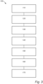
- Fig. 3 is a flow chart comprising steps of a method 100 according to an exemplary embodiment according to an aspect of the present disclosure.
- a method 100 for controlling an analog-to-digital converter, ADC, (not shown; see Fig. 1 ) is shown.
- the method 100 may comprise the step of supplying a predetermined first digital reference signal to a first capacitor bank of a first a digital-to-analog converter, DAC, of the ADC, wherein the first capacitor bank has N number of first capacitors and wherein first plates of the first capacitors of the N number of first capacitors are controlled by bits of the first digital reference signal.
- the method further comprises the step of supplying a predetermined second digital reference signal to a second capacitor bank of a second DAC, wherein the second capacitor bank has N number of second capacitors and wherein first plates of the second capacitors of the N number of second capacitors are controlled by bits of a second digital reference signal.
- the method further comprises the steps of supplying 110 a sampled first input signal of a differential input signal to second plates of the first capacitors and supplying 120 a sampled second input signal of a differential input signal to second plates of the second capacitors.
- a previous signal is subtracted by the step 130 of supplying the first digital reference signal to the first capacitor bank of the first DAC based on the previous signal and the step 140 of supplying the second digital reference signal to the second capacitor bank of the second DAC.
- the method further comprises the steps of supplying 150 first and second input voltage to first and second inputs of a comparator of the ADC, comparing 160 the first and second input voltages, and adjusting 170, based on a comparison of the first and second input voltages, the first or second digital reference signal so as to approximate a difference between the first and second input signals.
- the steps of comparing 160 and adjusting 170 may be performed multiple times until the difference between the first and second digital reference signals has sufficiently approximated the difference between the first and second input signals.
- the digital reference signals represent a signed binary value.
- the adjusting of the first or second digital reference signal may comprise selectively changing the first digital reference signal or the second digital reference signal in dependence of which of the first input voltage and the second input voltage is larger.
Landscapes
- Engineering & Computer Science (AREA)
- Theoretical Computer Science (AREA)
- Analogue/Digital Conversion (AREA)
Abstract
An analog-to-digital converter, ADC, (1) is provided. The ADC comprises a comparator (2) having a first input and a second input. The ADC further comprises a first digital-to-analog converter, DAC, (3) and a second DAC (4) configured to receive a first and a second digital reference signal, respectively. The digital reference signals (Dref) represent a signed binary value. The ADC is configured to compare input voltages (Vin), based on a first sampled input signal of a differential input signal and the first digital reference signal, and based on a second sampled input signal of the differential input signal and the second digital reference signal and, based on said comparison, adjust the reference voltage so as to approximate the differential input signal.
Description
- The present disclosure relates to the field of analog-to-digital converters, ADCs, and digital-to-analog-converters, DACs, used in ADCs.
- The project leading to this application has received funding from the European Research Council (ERC) under the European Union's Horizon 2020 research and innovation programme (grant agreement No 101001448).
- ADCs have been, and are currently, in use in almost every field of technology. As the size and power consumption of semiconductors has been steadily decreasing over the years while still providing potential computational power, the size and power consumption of electronic devices have correspondingly decreased. However, it has been observed that power consumption of ADCs has not been reduced to the same degree as the reduction of power consumption in semiconductors. As a consequence, a large portion of the power consumption of modern electronic devices comprising semiconductors and ADCs is attributed to the power consumption of ADCs. Such electronic devices may be configured as, for example, a sensor unit configured to continuously, or intermittently, measure a physical characteristic, i.e., analog data, convert said physical characteristic using an ADC to digital data, and store and/or transmit said digital data.
- One type of ADC is the Flash-ADC, which is, as the name infers, a fast type ADC. However, the Flash-ADC is very expensive with regards to power consumption. A more power efficient type of ADC is successive-approximation, SAR, ADCs. For sparse signals, power efficiency can be improved even more by decreasing the number of comparisons by using signal-dependent ADCs, such as a level-crossing ADC.
- A major portion of the power consumption of level-crossing ADCs is consumed by one or more comparisons of the ADC. In other words, a major portion of the power is consumed when comparing the input signal to a reference signal, in order to determine a value of the input signal.
- Therefore, it is of interest to provide a more power efficient ADC and a method for controlling an ADC which provides a more efficient power usage.
- An objective of the present disclosure is to provide an improved ADC and an improved DAC having decreased power consumptions, and a method for controlling said ADC.
- According to a first aspect of the present disclosure, an analog-to-digital converter, ADC, is provided. The ADC comprises a comparator having a first input and a second input, a first and a second digital-to-analog converter, DAC. The first DAC comprises a first capacitor bank having N number of first capacitors, wherein first plates of the first capacitors of the N number of first capacitors are controlled by bits of a first digital reference signal and wherein second plates of the first capacitors of the N number of first capacitors are configured to receive a sampled first input signal of a differential input signal. The second DAC comprises a second capacitor bank having N number of second capacitors, wherein first plates of the second capacitors of the N number of second capacitors are controlled by bits of a second digital reference signal and wherein second plates of the second capacitors of the N number of second capacitors are configured to receive a sampled second input signal of the differential input signal. The first and the second DAC are configured to supply first and second input voltages to the first and second inputs, respectively, of the comparator. The first and second digital reference signals represent a signed binary value. The ADC is configured to compare the first and the second input voltages. The ADC is further configured to, based on said comparison, adjust the first or second digital reference signal so as to approximate a difference between the first and the second input signals. The ADC may be configured to selectively change the first digital reference signal or the second digital reference signal in dependence of the comparison.
- According to a second aspect of the present disclosure, a method for controlling an analog-to-digital converter, ADC, is provided. The method according to the second aspect comprises the steps of supplying a first digital reference signal to a first capacitor bank of a first digital-to-analog converter, DAC, of the ADC, wherein the first capacitor bank has N number of first capacitors and wherein first plates of the first capacitors of the N number of first capacitors are controlled by bits of a first digital reference signal, supplying a second digital reference signal to a second capacitor bank of a second DAC, wherein the second capacitor bank has N number of second capacitors and wherein first plates of the second capacitors of the N number of second capacitors are controlled by bits of a second digital reference signal, supplying a sampled first input signal of a differential input signal to second plates of the first capacitors, supplying a sampled second input signal of a differential input signal to second plates of the second capacitors, supplying first and second input voltages to first and second inputs, respectively, of a comparator of the ADC, wherein the first input voltage is based on the first digital reference signal and the sampled first input signal and wherein the second input voltage is based on the second digital reference signal and the sampled second input signal, comparing the first and second input voltages, and adjusting, based on a comparison of the first and second input voltages, the first or second digital reference signal so as to approximate a difference between the first and the second input signals. The first and second digital reference signal represent a signed binary value in that each of the first and second digital reference signal represent a magnitude of the signed binary value and a sign of the signed binary value controls which of the first or the second digital reference signal that is to be adjusted.
- The present disclosure is based on the understanding that a vast amount of power, i.e., electrical energy or power, is consumed in a DAC when switching between different reference voltages provided to the DAC. Further, the present disclosure is based on the understanding that particular ADCs, such as an SAR ADC or a level-crossing ADC, utilize one or more capacitor banks, wherein the capacitors of a capacitor bank are configured to be charged based on a reference signal representing a binary signal. In such a capacitor bank, each capacitor is usually configured to correspond to a bit of the binary signal. Therefore, a capacitor which corresponds to a specific bit may have twice the capacitance of another capacitor which corresponds to a bit which is one step less significant than the specific bit. Consequently, the capacitor which corresponds to the most significant bit, MSB, may have the highest capacitance, and the capacitor which corresponds to the least significant bit, LSB, may have the lowest capacitance.
- The capacitors in the capacitor bank may be provided with a voltage (high/low) on a first plate representing a value of a corresponding bit of the digital reference signal. When adjusting a reference voltage representing the digital reference signal, it must be ensured the capacitors which corresponds to a bit set to a logical one are charged, and the capacitors which corresponds to a bit set to a logical zero are depleted, so as to make sure that the adjusted reference voltage correctly corresponds, or represents, the binary signal. Further, it has been realized that ADCs often start with a reference voltage which is in the middle of possible values that can be represented. Such a middle value may be represented by binary number equal to a logical one, 1, followed by zeroes, 0's, or phrased differently, the MSB may be equal to 1 and the remaining bits may be equal to 0. However, when determining a value of the input signal, , then the reference voltage may need to be decreased or increased in order to find a reference value that corresponds to the value of the input signal. A decrease of the reference voltage represented by the binary signal by the LSB of the binary signal, which equates to the MSB being equal to 0, and followed by all 1's, would cause all of the capacitors to have to change state, as the capacitor corresponding to the MSB, which has changed from 1 to 0, would be depleted and the remaining capacitors which were corresponding to bits equal to 0 would have to be charged as they would now be corresponding to bits equal to 1. Such charging and depletion of capacitors consumes a lot of power (i.e., electrical energy), especially for capacitors corresponding to the MSB and other more significant bits. The opposite situation, i.e., when the binary signal switches from all bits, except the MSB, being equal to 1 to all bits, except the MSB, being equal to 0, consequently also consumes a lot of power. Charging and/or depletion of a capacitor may, alternatively, be understood as switching of the capacitor. Further, charging the capacitor bank with the reference voltage corresponding to the digital reference signal at a first plate of the capacitors may be understood as pre-loading, and charging of the input signal onto a capacitor bank at a second plate of the capacitors may be understood as sampling.
- Many sensors measure phenomena which follows a regular pattern, rhythm, or frequency, such as a sensor for measuring a bodily function. If such measurements are put through a filter, such as a high-pass filter, the underlying regular pattern, rhythm, or frequency, may be at least partially extracted, and only abnormal events may be passed, which may be what is important or of interest to track, identify, and/or measure. Such filtered signals, or other signals having similar characteristics may be referenced to as sparse signals. The value of a sparse signal would be mostly having values close to a middle value, or common-mode value. If represented digitally, a vast majority of the values of a sparse signal may be within a few LSBs from each other. Converting such a sparse signal using a reference signal provided to capacitors would frequently cause capacitors switching, similar to the examples discussed in above, when the sparse signal would deviate a few LSBs below or a few LSBs above the middle value (i.e., represented by a binary signal for which the is MSB is equal 1, and the remaining bits are equal to 0). Thus, pre-loading of a capacitor bank may consume a lot of power in order to convert a sparse signal, even though the sparse signal does not comprise much information of interest.
- In light of the above understanding, it has been realized that it would be beneficial to reduce the amount of switching of capacitors of a DAC, and especially reducing the amount of switching of capacitors corresponding to more significant bits. Therefore, the present disclosure proposes the use of digital reference signal which represents a magnitude of a signed binary value. A signed binary value is a digital binary number for which the MSB defines the sign of the binary number, i.e., if the binary number is positive or negative. Correspondingly, the input signal may be represented as a signed signal, which may be performed at the measuring and/or at the sampling of the input signal. Therefore, when an input signal changes level, the amount of capacitors that may need to be switched is greatly reduced.
- The comparator is configured to receive a first input voltage and a second input voltage from the first DAC and the second DAC, respectively. Each DAC receives a sampled input signal on second plates and a digital reference signal on first plates, such that the digital reference signal will be converted to an analog value through a size of a respective capacitor representing a particular bit of the digital reference signal. The input voltage is then a sum of the sampled input signal and the reference signal.
- Adjusting the first or second digital reference signal so as to approximate a difference between the first and second input signals may be used for converting the differential input signal to a digital value. The first and second digital reference signal may represent the signed binary value which forms a digital representation of the difference between the sampled first input signal and the sampled second input signal.
- It should be realized that first plates of each capacitor of the capacitor banks may be controlled by a respective bit of the digital reference signal. However, in some embodiments, the capacitor bank may for most significant bits comprise two capacitors such that not all bits correspond to a single capacitor in the capacitor bank. This may be utilized such that the ADC may be configured to change both the first digital reference signal and the second digital reference signal when most significant bits are to be changed such that a common mode between the input voltages input to the comparator is not changed when most significant bits are changed.
- The signed binary value may have N+1 number of bits. Thus, the signed binary value may have one more bit than the capacitor bank has capacitors configured to generate a reference voltage based on the digital reference signal. The ADC may be further configured to selectively change the first digital reference signal or the second digital reference signal in dependence of which of the first input voltage and the second input voltage is larger. This may be understood as monotonic switching. Further, by selecting which of the first digital reference signal and the second digital reference signal is to be changed, the selection represents the most significant bit, MSB, of the signed binary value. The first digital reference signal and the second digital reference signal form a magnitude of the signed binary value. This implies that, thanks to the selective change of the first digital reference signal or the second digital reference signal, one less capacitor may be used than the number of bits to be represented.
- The capacitor that may be omitted may be the one that would have been corresponding to the MSB, which may have the highest capacitance. Therefore, if a sparse signal would change between from a value a few LSBs below a middle value to a few LSBs above a middle value, then only capacitors corresponding to a few LSBs of the signed binary value would have to be switched, as the MSB of the signed binary value would instead be represented by which of the first or the second digital reference signal that is changed.
- Each capacitor of the N number of capacitors may be controlled by a corresponding bit of the digital reference signal.
- A first capacitor of each of the first and second capacitor banks may be controlled based on a least significant bit, LSB, of the first and second digital reference signal, respectively, and a subsequent capacitor may be controlled based on a bit of the first and second digital reference signal, respectively, which is subsequent to the bit for which control of a capacitor which is directly prior to said subsequent capacitor is based on. A subsequent capacitor may have a capacitance twice that of a capacitor which is directly prior to said subsequent capacitor. Therefore, avoiding switching of a capacitors which are controlled based on more significant bits saves more power than avoiding switching of capacitors which are controlled based on less significant bits. Thereby, by controlling capacitors based on signed binary values, the amount of switching of capacitors controlled based on more significant bits may be reduced, especially for sparse signals.
- It should be realized that the capacitors need not necessarily have different sizes. For instance, as an alternative, the capacitors may each have an equal size and the digital reference signal may be represented by a thermometer code.
- Adjusting the first digital reference signal or the second digital reference signal so as to approximate the difference between the first and second input signals may comprise increasing the signed binary value by one least significant bit, LSB, and adjusting the first digital reference signal or the second digital reference signal based on the increased signed binary value. In a next step, the adjusting may adjust a second least significant bit and so on until the comparator identifies a shift in which of the first or the second input voltages is larger. After this, a normal SAR search starting from a last checked bit towards the LSB may be performed in order to find the binary representation of the differential input signal.
- Such an approach may be understood as an LSB-first approach. An LSB-first approach may be more power efficient, especially for an ADC converting a sparse signal.
- Adjusting the first digital reference signal or the second digital reference signal so as to approximate the difference between the first and second signals may utilize first digital reference signal and second digital reference signal of a previously sampled value. Thus, the first digital reference signal and the second digital reference signal may be set based on the previously sampled value. When a subsequent sampled value is to be converted, the differential input signal may be compared to at least one of an upper threshold or a lower threshold. The upper threshold and the lower threshold may correspond to changing the least significant bit of the first digital reference signal or the second digital reference signal, respectively.
- Such an approach may be understood as a level-crossing ADC. A level-crossing ADC may be more power efficient, especially for an ADC converting a sparse signal.
- The ADC may further comprise circuitry configured to calculate the signed binary value. The circuitry may be understood as logic circuitry. The logic circuitry may be configured to output digital signals based on, at least, the comparisons of comparator. The digital signals may be used to digitally recreate (an approximation of) the analog input signal. The logic circuit may further be configured to deliver the digital reference signals and/or the signed binary value to the DACs of the ADC.
- The ADC and other circuitry connected to the ADC may be configured to operate using sign-magnitude representation of values. This implies that no conversion between signed binary values and unsigned binary values is needed.
- The ADC may further comprise a sample-and-hold circuit configured to provide the input signal to the DAC. The sample-and-hold circuit may be configured to receive output from a sensor and may be configured to sample-and-hold the output, wherein the held output may be understood as the input signal. The sample-and-hold circuit may be configured to receive a filtered output or may be configured to filter an output signal before sampling and holding said filtered output signal.
- The present disclosure relates to all possible combinations of features recited in the claims. Objects and features described according to the first aspect may be combinable with, or replaced by, objects and features described according to the second aspect, the third aspect, and/or the fourth aspect, and vice versa.
- Further objects and advantages of the various examples of the present disclosure will be described below by means of exemplifying embodiments.
- The above, as well as additional objects, features, and advantages of the present disclosure, will be better understood through the following illustrative and non-limiting detailed description, with reference to the appended drawings. In the drawings like reference numerals will be used for like elements unless stated otherwise.
-
Fig. 1 is a schematic view of an ADC according to an exemplary embodiment of the present disclosure. -
Fig. 2 is a schematic view of a capacitor bank and a comparator according to an exemplary embodiment of the present disclosure. -
Fig. 3 is a flow chart comprising steps of a method according to an exemplary embodiment according to an aspect of the present disclosure. - Unless explicitly stated to the contrary, the drawings show only such elements that are necessary to illustrate the example embodiments, while other elements, in the interest of clarity, may be omitted or merely suggested. As illustrated in the figures, the sizes of elements and regions may be exaggerated for illustrative purposes and, thus, are provided to illustrate the general structures of the embodiments.
-
Fig. 1 illustrates an ADC 1 according to an exemplary embodiment of the present disclosure. The ADC 1 comprises a comparator 2 having a first input and a second input. The first input is illustrated inFig. 1 as a plus symbol, "+", and the second input is illustrated inFig. 1 as a minus symbol, "-". However, the illustration is purely exemplary, and the first input and the second input may be switched. - The ADC 1 may comprise a sample-and-hold circuit 5, which may be configured to supply a sampled and held differential input signal. The sampled and held differential input signal provides a first input signal Vinp and a second input signal Vinn. The first input signal Vinp may be provided with a first reference voltage to the first input to the comparator 2 and the second input signal Vinn may be provided with a second reference voltage to the second input of the comparator 2.
- It should be realized that an input signal Vin provided to the sample-and-hold circuit 5 need not be a differential signal but may alternatively be a single-ended signal. The sample-and-hold circuit 5 may still be configured to generate a differential input signal to the ADC 1. For instance, the first input signal Vinp may correspond to a single-ended input signal Vin, whereas the second input signal Vinn may be 0, whereby the ADC 1 configured to convert the differential input signal Vinp - Vinn to a digital format will provide a conversion of Vin to digital format as Vin = Vinp - Vinn.
- The ADC 1 further comprises a first digital-to-analog converter, DAC, 3 configured to supply the first reference voltage to the first input of the comparator 2 and a second DAC 4 configured to supply the second reference voltage to the second input of the comparator 2.
- The ADC 1 is configured to compare the first input voltage and the second input voltage using the comparator 2, and, based on said comparison, adjust the first or second reference voltage so as to approximate the difference between the first and second input signals Vinp and Vinn. The ADC 1 may be configured adjust the first or the second reference voltage multiple times until a sufficient approximation has been acquired.
- Each of the first and second reference voltages is based on a digital reference signal Dref, wherein the digital reference signal Dref represents a signed binary value. The digital reference signal Dref may be determined by a
logic circuit 6 of the ADC 1. A most significant bit of the digital reference signal Dref may control which of the first and second reference voltages that is to be adjusted so as to determine whether a first or a second digital reference signal provided to the first DAC 3 and the second DAC 4, respectively, is to be changed. Each of the first DAC 3 and the second DAC 4 may be configured to convert the first and a second digital reference signal, respectively, to the first and second reference voltages. - The
logic circuit 6 may be configured to adjust or update the digital reference signal Dref based on comparison of the comparator 2. Further, thelogic circuit 6 may be configured to output one ormore signals 30, from which (approximation of) a digital version of the input signal Vin may be recreated. - The first and second reference voltages are supplied via capacitor banks (not shown; see
Fig. 2 ) of the first and second DACs 3, 4, each having N number of capacitors. Each capacitor of the N number of capacitors is controlled by a corresponding bit of a magnitude of the signed binary value represented by the digital reference signal Dref. - The
logic circuit 6 may be configured to determine the signed binary value based on, at least, comparisons of the comparator 2. The signed binary value may have N+1 number of bits. In other words, the signed binary value may have one more bit than the number of capacitors configured to supply the respective reference voltages. Further, ADC 1 may be configured to determine for which of the first and second DAC 3, 4, the reference voltage reference should be changed, based on a most significant bit, MSB, of the digital reference signal Dref which represents the signed binary value. - For instance, the first DAC 3 and the second DAC 4 may be set to provide a first reference voltage and a second reference voltage which is each equal to zero. This implies that the comparator 2 may be configured to compare Vinp > Vinn. If Vinp is smaller than Vinn, the first digital reference signal may be increased by 1, i.e., a LSB is increased, corresponding to 1/64*Vref if the signed binary value is represented by 7 bits. This implies that the comparator 2 will be configured to compare Vinp + 1/64*Vref > Vinn in a subsequent comparison. If on the other hand, Vinp is larger than Vinn, the second digital reference signal may be increased by 1 and the comparator 2 will be configured to compare Vinp > Vinn + 1/64*Vref.
-
Fig. 2 is a schematic view of afirst capacitor bank 10 and asecond capacitor bank 12, each comprising a plurality of capacitors C0-C5 and a comparator 2 according to an exemplary embodiment of the present disclosure. - The
capacitor banks Fig. 2 may be understood as being part of a DAC of an ADC (not shown; seeFig. 1 ) according to the present disclosure. However, it is to be understood that the showncapacitor banks - Each
capacitor bank capacitor banks - The six capacitors C0-C5 of the first and
second capacitor banks - Further, the difference in capacitance between two capacitors of the six capacitors C0-C5 may be equal to the difference in value which the two bits which controls said two capacitors. Thus, the third capacitor C2 may have twice the capacitance of the second capacitor C1, which may in turn have twice the capacitance of the first capacitor C0. This ensures that level of the reference voltage corresponds to the value of the digital reference signal.
- The capacitors C0-C5 of the
first capacitor bank 10 are shown to be connected to the first input of the comparator 2 with the first digital reference signal provided to first plates of the capacitors C0-C5. It may be understood that a first sampled input signal (not shown; seeFig. 1 ) may be provided to second plates of the capacitors C0-C5 and further connected to the first input of the comparator 2 which thus receives the first sampled input signal and the first reference voltage based on the first digital reference signal as input. - The capacitors C0-C5 of the
second capacitor bank 12 are shown to be connected to the second input of the comparator 2 with the second digital reference signal provided to first plates of the capacitors C0-C5. It may be understood that a second sampled input signal (not shown; seeFig. 1 ) may be provided to second plates of the capacitors C0-C5 and further connected to the second input of the comparator 2 which thus receives the second sampled input signal and the second reference voltage based on the second digital reference signal as input. -
Fig. 3 is a flow chart comprising steps of amethod 100 according to an exemplary embodiment according to an aspect of the present disclosure. - A
method 100 for controlling an analog-to-digital converter, ADC, (not shown; seeFig. 1 ) is shown. Themethod 100 may comprise the step of supplying a predetermined first digital reference signal to a first capacitor bank of a first a digital-to-analog converter, DAC, of the ADC, wherein the first capacitor bank has N number of first capacitors and wherein first plates of the first capacitors of the N number of first capacitors are controlled by bits of the first digital reference signal. The method further comprises the step of supplying a predetermined second digital reference signal to a second capacitor bank of a second DAC, wherein the second capacitor bank has N number of second capacitors and wherein first plates of the second capacitors of the N number of second capacitors are controlled by bits of a second digital reference signal. The method further comprises the steps of supplying 110 a sampled first input signal of a differential input signal to second plates of the first capacitors and supplying 120 a sampled second input signal of a differential input signal to second plates of the second capacitors. - After the differential input signal is sampled, a previous signal is subtracted by the
step 130 of supplying the first digital reference signal to the first capacitor bank of the first DAC based on the previous signal and thestep 140 of supplying the second digital reference signal to the second capacitor bank of the second DAC. - The method further comprises the steps of supplying 150 first and second input voltage to first and second inputs of a comparator of the ADC, comparing 160 the first and second input voltages, and adjusting 170, based on a comparison of the first and second input voltages, the first or second digital reference signal so as to approximate a difference between the first and second input signals. The steps of comparing 160 and adjusting 170 may be performed multiple times until the difference between the first and second digital reference signals has sufficiently approximated the difference between the first and second input signals. The digital reference signals represent a signed binary value.
- The adjusting of the first or second digital reference signal may comprise selectively changing the first digital reference signal or the second digital reference signal in dependence of which of the first input voltage and the second input voltage is larger.
- In the above the inventive concept has mainly been described with reference to a limited number of examples. However, as is readily appreciated by a person skilled in the art, other examples than the ones disclosed above are equally possible within the scope of the present disclosure.
Claims (13)
- An analog-to-digital converter, ADC, (1) comprising:a comparator (2) having a first input and a second input;a first digital-to-analog converter, DAC, (3) comprising a first capacitor bank (10) having N number of first capacitors, wherein first plates of the first capacitors of the N number of first capacitors are controlled by bits of a first digital reference signal and wherein second plates of the first capacitors of the N number of first capacitors are configured to receive a sampled first input signal of a differential input signal, wherein the first digital reference signal represents a signed binary value, and wherein the first DAC (3) is configured to supply a first input voltage to the first input of the comparator (2); anda second DAC (4), comprising a second capacitor bank (12) having N number of second capacitors, wherein first plates of the second capacitors of the N number of first capacitors are controlled by bits of a second digital reference signal and wherein second plates of the second capacitors of the N number of second capacitors are configured to receive a sampled second input signal of the differential input signal, wherein the second digital reference signal represents a signed binary value, and wherein the second DAC (4) is configured to supply a second input voltage to the second input of the comparator (2);wherein the ADC (1) is configured to compare the first and second input voltages and, based on said comparison, adjust the first digital reference signal or the second digital reference signal so as to approximate a difference between the first and second input signals; andwherein the ADC (1) is configured to selectively change the first digital reference signal or the second digital reference signal in dependence of said comparison.
- The ADC according to claim 1, wherein the signed binary value has N+1 number of bits;
wherein the ADC (1) is further configured to selectively change the first digital reference signal or the second digital reference signal in dependence of which of the first input voltage and the second input voltage is larger. - The ADC according to claim 1 or 2, wherein a first capacitor of each of the first and second capacitor banks (10, 12) is controlled based on a least significant bit, LSB, of the first and second digital reference signal, respectively, and
a subsequent capacitor is controlled based on a bit of the first and second digital reference signal, respectively, which is subsequent to the bit for which control of a capacitor which is directly prior to said subsequent capacitor is based on. - The ADC according to claim 3, wherein a subsequent capacitor has a capacitance twice that of a capacitor which is directly prior to said subsequent capacitor.
- The ADC according to any one of claims 1 to 4, wherein the ADC (1) being configured to adjust the first digital reference signal or the second digital reference signal so as to approximate the difference between the first and second input signals comprises: increasing the signed binary value by one least significant bit, LSB, and adjusting the first digital reference signal or the second digital reference signal based on the increased signed binary value.
- The ADC according to any one of claims 1 to 4, wherein the ADC (1) being configured to set the first digital reference signal and the second digital reference signal based on the differential input signal sampled during a first sampling period and compare the differential input signal sampled during a second sampling period to at least one of an upper threshold or a lower threshold for determining whether a level-crossing occurred.
- The ADC according to any one of claims 1 to 6, further comprising circuitry (6) configured to calculate the signed binary value.
- The ADC according to any one of claims 1 to 7, further comprising a sample-and-hold, S&H, circuit (5) configured to provide the input signal to the DAC.
- A method (100) for controlling an analog-to-digital converter, ADC, comprising the steps of:supplying (130) a first digital reference signal to a first capacitor bank of a first digital-to-analog converter, DAC, of the ADC, wherein the first capacitor bank has N number of first capacitors and wherein first plates of the first capacitors of N number of first capacitors are controlled by bits of a first digital reference signal,supplying (140) a second digital reference signal to a second capacitor bank of a second DAC, wherein the second capacitor bank has N number of second capacitors and wherein first plates of the second capacitors of the N number of second capacitors are controlled by bits of a second digital reference signal,supplying (110) a sampled first input signal of a differential input signal to second plates of the first capacitors,supplying (120) a sampled second input signal of a differential input signal to second plates of the second capacitors;supplying (150) first and second input voltages to first and second inputs, respectively, of a comparator of the ADC, wherein the first input voltage is based on the first digital reference signal and the sampled first input signal and wherein the second input voltage is based on the second digital reference signal and the sampled second input signal;comparing (160) the first and second input voltages; andadjusting (170), based on a comparison of the first and second input voltages, the first or second digital reference signal so as to approximate a difference between the first and second input signals;wherein the first and second digital reference signals represent a signed binary value.
- The method according to claim 9, wherein the signed binary value has N+1 number of bits; and
wherein the method further comprises to selectively change the first digital reference signal or the second digital reference signal in dependence of which of the first input voltage and the second input voltage is larger. - The method according to claim 9 or 10, wherein a first capacitor of each of the first and second capacitor banks is controlled based on a least significant bit, LSB, of the first and second digital reference signal, respectively, anda subsequent capacitor is controlled based on a bit of the first and second digital reference signal, respectively, which is subsequent to the bit for which control of a capacitor which is directly prior to said subsequent capacitor is based on; andwherein a subsequent capacitor has a capacitance twice that of a capacitor which is directly prior to said subsequent capacitor.
- The method according to any one of claims 9 to 11, wherein the step of adjusting the first digital reference signal or the second digital reference signal comprises increasing the signed binary value by one least significant bit, LSB, and adjusting the first digital reference signal or the second digital reference signal based on the increased signed binary value.
- The method according to any one of claims 9 to 11, wherein the step of adjusting the first digital reference signal or the second digital reference signal so as to approximate the difference between the first and second signals utilizes first digital reference signal and second digital reference signal of a previously sampled value, and for a subsequent sample of the differential input signal, the differential input signal may be compared to at least one of an upper threshold or a lower threshold.
Priority Applications (3)
| Application Number | Priority Date | Filing Date | Title |
|---|---|---|---|
| EP22214802.5A EP4391386A1 (en) | 2022-12-20 | 2022-12-20 | An analog-to-digital converter, adc, a method for controlling said adc, and a method for controlling a digital-analog-converter for said adc |
| CN202311647859.7A CN118232919A (en) | 2022-12-20 | 2023-12-01 | Analog-to-digital converter ADC, method for controlling said ADC |
| US18/527,683 US12603661B2 (en) | 2022-12-20 | 2023-12-04 | Analog-to-digital converter, ADC, a method for controlling said ADC, and a method for controlling a digital-analog-converter for said ADC |
Applications Claiming Priority (1)
| Application Number | Priority Date | Filing Date | Title |
|---|---|---|---|
| EP22214802.5A EP4391386A1 (en) | 2022-12-20 | 2022-12-20 | An analog-to-digital converter, adc, a method for controlling said adc, and a method for controlling a digital-analog-converter for said adc |
Publications (1)
| Publication Number | Publication Date |
|---|---|
| EP4391386A1 true EP4391386A1 (en) | 2024-06-26 |
Family
ID=84541457
Family Applications (1)
| Application Number | Title | Priority Date | Filing Date |
|---|---|---|---|
| EP22214802.5A Pending EP4391386A1 (en) | 2022-12-20 | 2022-12-20 | An analog-to-digital converter, adc, a method for controlling said adc, and a method for controlling a digital-analog-converter for said adc |
Country Status (3)
| Country | Link |
|---|---|
| US (1) | US12603661B2 (en) |
| EP (1) | EP4391386A1 (en) |
| CN (1) | CN118232919A (en) |
Families Citing this family (1)
| Publication number | Priority date | Publication date | Assignee | Title |
|---|---|---|---|---|
| CN120074526B (en) * | 2025-04-28 | 2025-08-12 | 瑞纳智能设备股份有限公司 | Signal acquisition circuit and signal acquisition method |
Family Cites Families (28)
| Publication number | Priority date | Publication date | Assignee | Title |
|---|---|---|---|---|
| KR101007063B1 (en) * | 2008-10-31 | 2011-01-12 | 한국과학기술원 | Digital error correction method and apparatus of SAR type analog / digital converter |
| EP2296280B1 (en) * | 2009-09-10 | 2012-12-19 | Stichting IMEC Nederland | Asynchronous SAR ADC |
| US8514114B2 (en) * | 2011-06-02 | 2013-08-20 | Analog Devices, Inc. | Measurement method and apparatus for ADC calibration |
| US8471751B2 (en) * | 2011-06-30 | 2013-06-25 | Intel Corporation | Two-stage analog-to-digital converter using SAR and TDC |
| US9148603B2 (en) * | 2012-05-15 | 2015-09-29 | Semiconductor Components Industries, Llc | Offset injection in an analog-to-digital converter |
| US8928506B2 (en) * | 2013-04-09 | 2015-01-06 | Maxlinear, Inc. | Successive approximation analog-to-digital converter (ADC) with dynamic search algorithm |
| US9048860B1 (en) * | 2014-06-05 | 2015-06-02 | Xilinx, Inc. | Successive approximation analog-to-digital conversion |
| CN107113003B (en) * | 2014-10-23 | 2019-04-19 | 美国莱迪思半导体公司 | Analog-to-digital converter based on successive approximation register |
| US9432037B2 (en) * | 2014-11-05 | 2016-08-30 | Samsung Electronics Co., Ltd | Apparatus and method for analog-digital converting |
| EP3059867B1 (en) * | 2015-02-19 | 2020-07-08 | Stichting IMEC Nederland | Circuit and method for dac mismatch error detection and correction in an adc |
| KR101670440B1 (en) * | 2015-05-07 | 2016-10-28 | 고려대학교 산학협력단 | Low power, high speed successive approximated register analog to digital converter and method for converting using the same |
| KR20180105027A (en) * | 2017-03-14 | 2018-09-27 | 에스케이하이닉스 주식회사 | Successive approximation register analog-digital converter having split-capacitor based digital-analog converter |
| US10511320B2 (en) * | 2017-09-28 | 2019-12-17 | Taiwan Semiconductor Manufacturing Company Limited | Low distortion successive approximation register (SAR) analog-to-digital converters (ADCs) and associated methods |
| TWI649978B (en) * | 2017-10-24 | 2019-02-01 | 財團法人工業技術研究院 | Continuous approximation register analog to digital converter and its operation method |
| WO2019100036A1 (en) * | 2017-11-20 | 2019-05-23 | The Regents Of The University Of California | Memristive neural network computing engine using cmos-compatible charge-trap-transistor (ctt) |
| US10425095B1 (en) * | 2018-08-27 | 2019-09-24 | Qualcomm Incorporated | Multiple-bit parallel successive approximation (SA) flash analog-to-digital converter (ADC) circuits |
| CN109217874B (en) * | 2018-11-16 | 2020-11-17 | 深圳锐越微技术有限公司 | Margin transfer loop, successive approximation type analog-to-digital converter and gain calibration method |
| US10476513B1 (en) * | 2018-11-19 | 2019-11-12 | Ncku Research And Development Foundation | SAR ADC with high linearity |
| TWI698091B (en) * | 2018-12-12 | 2020-07-01 | 瑞昱半導體股份有限公司 | Successive approximation register analog-to-digital converter and operation method thereof |
| CN110324043B (en) * | 2019-04-24 | 2023-06-30 | 矽力杰半导体技术(杭州)有限公司 | Pseudo-differential analog-to-digital converter |
| CN111865318B (en) * | 2019-04-30 | 2024-06-21 | 瑞昱半导体股份有限公司 | Analog-digital conversion device and capacitance adjusting method thereof |
| TWI685210B (en) * | 2019-06-14 | 2020-02-11 | 瑞昱半導體股份有限公司 | Successive approximation register analog-to-digital converter and operation method thereof |
| US10790842B1 (en) * | 2019-10-31 | 2020-09-29 | Infineon Technologies Ag | System and method for a successive approximation analog-to-digital converter |
| US11239853B1 (en) * | 2020-10-28 | 2022-02-01 | Digital Analog Integration, Inc. | Hybrid analog-to-digital converter with multi-domain signal processing |
| TWI800817B (en) * | 2021-04-15 | 2023-05-01 | 瑞昱半導體股份有限公司 | Analog-to-digital converter and method thereof |
| US12212334B2 (en) * | 2022-03-21 | 2025-01-28 | Avago Technologies International Sales Pte. Limited | Successive approximation register analog to digital converter having adaptive current or voltage parameter adjustments |
| US12316339B2 (en) * | 2023-03-24 | 2025-05-27 | Qualcomm Incorporated | Input-adaptive analog-to-digital conversion |
| TWI864839B (en) * | 2023-06-20 | 2024-12-01 | 瑞昱半導體股份有限公司 | Time interleaved analog to digital converter and signal conversion method |
-
2022
- 2022-12-20 EP EP22214802.5A patent/EP4391386A1/en active Pending
-
2023
- 2023-12-01 CN CN202311647859.7A patent/CN118232919A/en active Pending
- 2023-12-04 US US18/527,683 patent/US12603661B2/en active Active
Non-Patent Citations (4)
| Title |
|---|
| DING ZHAOMING ET AL: "Delta-Measurement Low-Power SAR ADC Architecture with Adaptive Threshold-First Switching", 2018 IEEE INTERNATIONAL SYMPOSIUM ON CIRCUITS AND SYSTEMS (ISCAS), IEEE, 27 May 2018 (2018-05-27), pages 1 - 4, XP033434626, DOI: 10.1109/ISCAS.2018.8351179 * |
| LEE B-G ET AL: "Input-tracking DAC for low-power high-linearity SAR ADC", ELECTRONIC LETTERS, THE INSTITUTION OF ENGINEERING AND TECHNOLOGY, vol. 47, no. 16, 4 August 2011 (2011-08-04), pages 911 - 913, XP006039173, ISSN: 1350-911X, DOI: 10.1049/EL:20111642 * |
| SONG YAN ET AL: "A 0.6-V 10-bit 200-kS/s Fully Differential SAR ADC With Incremental Converting Algorithm for Energy Efficient Applications", IEEE TRANSACTIONS ON CIRCUITS AND SYSTEMS I: REGULAR PAPERS, IEEE, US, vol. 63, no. 4, 1 April 2016 (2016-04-01), pages 449 - 458, XP011607277, ISSN: 1549-8328, [retrieved on 20160418], DOI: 10.1109/TCSI.2016.2528080 * |
| YAUL FRANK M ET AL: "A 10 bit SAR ADC With Data-Dependent Energy Reduction Using LSB-First Successive Approximation", IEEE JOURNAL OF SOLID-STATE CIRCUITS, IEEE, USA, vol. 49, no. 12, 1 December 2014 (2014-12-01), pages 2825 - 2834, XP011564898, ISSN: 0018-9200, [retrieved on 20141120], DOI: 10.1109/JSSC.2014.2352304 * |
Also Published As
| Publication number | Publication date |
|---|---|
| US12603661B2 (en) | 2026-04-14 |
| US20240204794A1 (en) | 2024-06-20 |
| CN118232919A (en) | 2024-06-21 |
Similar Documents
| Publication | Publication Date | Title |
|---|---|---|
| US10135457B2 (en) | Successive approximation register analog-digital converter having a split-capacitor based digital-analog converter | |
| US11418209B2 (en) | Signal conversion circuit utilizing switched capacitors | |
| US8599059B1 (en) | Successive approximation register analog-digital converter and method for operating the same | |
| US7956787B2 (en) | SAR analog-to-digital converter having differing bit modes of operation | |
| US11349492B2 (en) | Analog-to-digital converter | |
| KR101191054B1 (en) | Analog-to-digital converter with offset voltage calibration method | |
| CN107996019A (en) | A kind of DAC capacitor arrays, SAR type analog-to-digital converter and the method for reducing power consumption | |
| US20130147649A1 (en) | Analogue to Digital Converter, An Integrated Circuit and Medical Device | |
| WO2011028674A2 (en) | Low-power area-efficient sar adc using dual capacitor arrays | |
| US8004448B2 (en) | Dual DAC structure for charge redistributed ADC | |
| CN111371457B (en) | An analog-to-digital converter and a three-level switching method applied to SAR ADC | |
| CN111130550B (en) | Successive approximation register type analog-to-digital converter and signal conversion method thereof | |
| CN108631778B (en) | Successive approximation analog-to-digital converter and conversion method | |
| CN103095299A (en) | Weight estimation method, device and analog-to-digital converter using same | |
| US12603661B2 (en) | Analog-to-digital converter, ADC, a method for controlling said ADC, and a method for controlling a digital-analog-converter for said ADC | |
| EP3607659B1 (en) | Successive approximation register (sar) analog to digital converter (adc) dynamic range extension | |
| KR101056380B1 (en) | SAR analog-to-digital converter | |
| KR101986699B1 (en) | Successive approximation register analog digital converter and operating method thereof | |
| CN111865318B (en) | Analog-digital conversion device and capacitance adjusting method thereof | |
| CN113612482B (en) | Single-ended successive approximation register type analog-to-digital converter circuit | |
| CN114244358A (en) | Pipeline successive approximation analog-to-digital conversion circuit | |
| CN109039338B (en) | Differential capacitor array and switching method thereof | |
| Liu et al. | A fully differential SAR/single-slope ADC for CMOS imager sensor | |
| JPH1070463A (en) | Analog / digital conversion circuit | |
| CN110266312A (en) | A DAC switching method applied to SAR ADC |
Legal Events
| Date | Code | Title | Description |
|---|---|---|---|
| PUAI | Public reference made under article 153(3) epc to a published international application that has entered the european phase |
Free format text: ORIGINAL CODE: 0009012 |
|
| STAA | Information on the status of an ep patent application or granted ep patent |
Free format text: STATUS: THE APPLICATION HAS BEEN PUBLISHED |
|
| AK | Designated contracting states |
Kind code of ref document: A1 Designated state(s): AL AT BE BG CH CY CZ DE DK EE ES FI FR GB GR HR HU IE IS IT LI LT LU LV MC ME MK MT NL NO PL PT RO RS SE SI SK SM TR |
|
| STAA | Information on the status of an ep patent application or granted ep patent |
Free format text: STATUS: REQUEST FOR EXAMINATION WAS MADE |
|
| 17P | Request for examination filed |
Effective date: 20241219 |