EP4391384A1 - Pegelschieber und schaltungen mit mehreren spannungsdomänen - Google Patents
Pegelschieber und schaltungen mit mehreren spannungsdomänen Download PDFInfo
- Publication number
- EP4391384A1 EP4391384A1 EP23175334.4A EP23175334A EP4391384A1 EP 4391384 A1 EP4391384 A1 EP 4391384A1 EP 23175334 A EP23175334 A EP 23175334A EP 4391384 A1 EP4391384 A1 EP 4391384A1
- Authority
- EP
- European Patent Office
- Prior art keywords
- voltage
- circuit
- offset
- bias
- fet
- Prior art date
- Legal status (The legal status is an assumption and is not a legal conclusion. Google has not performed a legal analysis and makes no representation as to the accuracy of the status listed.)
- Pending
Links
- 239000003990 capacitor Substances 0.000 claims description 3
- 230000003019 stabilising effect Effects 0.000 abstract 1
- 238000010586 diagram Methods 0.000 description 5
- 238000002955 isolation Methods 0.000 description 2
- 238000000034 method Methods 0.000 description 2
- 238000012986 modification Methods 0.000 description 2
- 230000004048 modification Effects 0.000 description 2
- 230000001419 dependent effect Effects 0.000 description 1
- 238000007726 management method Methods 0.000 description 1
Images



Classifications
-
- H—ELECTRICITY
- H03—ELECTRONIC CIRCUITRY
- H03K—PULSE TECHNIQUE
- H03K19/00—Logic circuits, i.e. having at least two inputs acting on one output; Inverting circuits
- H03K19/0175—Coupling arrangements; Interface arrangements
- H03K19/0185—Coupling arrangements; Interface arrangements using field effect transistors only
- H03K19/018507—Interface arrangements
-
- H—ELECTRICITY
- H03—ELECTRONIC CIRCUITRY
- H03K—PULSE TECHNIQUE
- H03K19/00—Logic circuits, i.e. having at least two inputs acting on one output; Inverting circuits
- H03K19/0175—Coupling arrangements; Interface arrangements
- H03K19/0185—Coupling arrangements; Interface arrangements using field effect transistors only
- H03K19/018557—Coupling arrangements; Impedance matching circuits
-
- H—ELECTRICITY
- H03—ELECTRONIC CIRCUITRY
- H03K—PULSE TECHNIQUE
- H03K17/00—Electronic switching or gating, i.e. not by contact-making and –breaking
- H03K17/51—Electronic switching or gating, i.e. not by contact-making and –breaking characterised by the components used
- H03K17/56—Electronic switching or gating, i.e. not by contact-making and –breaking characterised by the components used by the use, as active elements, of semiconductor devices
- H03K17/687—Electronic switching or gating, i.e. not by contact-making and –breaking characterised by the components used by the use, as active elements, of semiconductor devices the devices being field-effect transistors
-
- H—ELECTRICITY
- H03—ELECTRONIC CIRCUITRY
- H03K—PULSE TECHNIQUE
- H03K19/00—Logic circuits, i.e. having at least two inputs acting on one output; Inverting circuits
- H03K19/003—Modifications for increasing the reliability for protection
- H03K19/00369—Modifications for compensating variations of temperature, supply voltage or other physical parameters
- H03K19/00384—Modifications for compensating variations of temperature, supply voltage or other physical parameters in field effect transistor circuits
Definitions
- the present disclosure relates to level shifters, and to electronic circuits such as multi-voltage domain circuits, for level shifters and other applications.
- a conceptual level shifter 100 is shown in FIG. 1 .
- the level shifter 100 is connected to a reference voltage which may be a ground voltage 110 at 0V as shown, and includes a low-level voltage rail V A 120.
- An input signal IN 130 which may be a digital signal, is provided between ground 110 and V A 120.
- V A 120 may be a fixed voltage rail, or may simply be a "high" value of the input signal IN 130.
- a typical value for V A may be 5V as discussed above
- Level shifter 100 is also connected to a high-voltage rail or input V B 140.
- V B may be, as mentioned above 24V, 48V or even higher.
- V B defines a "high-voltage domain".
- the function of the level shifter 100 is to "shift" the voltage level of the input signal IN 130 (which is between 0 V and 5 V in this instance) to provide an output OUT 160 in the high voltage domain such that (referenced to ground), instead of varying between 0 and 5 V, it varies between V B and another voltage V C 150, which is tied to V B .
- V C may be 48V - 5V, that is to say 43 V.
- V B - V C the voltage swing in the higher domain need not be the same as that (V A - GND) in the low domain.
- V B - V C the voltage swing in the higher domain need not be the same as that (V A - GND) in the low domain.
- variable in the case of a binary digital signal, “vary” corresponds to switching between the two levels.
- the present disclosure is not limited to binary digital switching, so the signals IN 130 and OUT 160 may include intermediate values between the high and the low value or even may vary in an analogue fashion.
- an electronic circuit configured to switchably generate an offset-bias output at a offset-bias voltage (Vc) in response to at least an enable signal (EN) at a low voltage relative to the offset-bias voltage, and comprising: a reference input terminal, configured to be connected to a reference voltage (GND); a low-voltage-input terminal, configured to receive the enable signal at a first voltage; a high-voltage-supply terminal, configured to receive power at a second voltage (V B ); an offset-bias output terminal (526), configured to output the offset-bias output, wherein the offset-bias voltage is less than the second voltage; a voltage-offset circuit (510) configured to generate the offset-bias voltage from the second voltage; a bias circuit (530) configured to switchably provide a bias current (lb1) to the voltage-offset circuit; and a high-voltage stand-off circuit (550), connected between the bias circuit and the voltage-offset circuit and configured to withstand
- Such a circuit may enable a stable output voltage difference VB-VC in the high voltage domain, and in particular one which is relatively insensitive to changes in process, voltage and temperature (PVT).
- PVT process, voltage and temperature
- the electronic circuit may further comprise a pull-up circuit (540) configured to tie the bias voltage to the second voltage in response to the enable signal not enabling the electronic circuit.
- a pull-up circuit (540) configured to tie the bias voltage to the second voltage in response to the enable signal not enabling the electronic circuit.
- Vc voltage of the offset-bias output from floating when the circuit is not enabled.
- each p-FET of the plurality of series-connected FETs is configured to be diode-connected by having its drain connected to its respective gate. This may help to stabilise the voltage across the respective FET.
- M 3. In other embodiments, M may have a different value and in particular may be equal to 2 or 4. This may provide for a choice of the value of the difference between V B and Vc.
- N 1, and the source of the n-FET is connected to the high-voltage-supply terminal, and a drain of the n-FET is connected to the offset-bias output terminal.
- N 2, such that there is a first n-FET and a second n-FET, a gate of the first n-FET is connected to the gate of the further p-FET, the drain of the first n-FET is connected to a gate of a second n-FET, the drain of the second n-FET is connected to the offset-bias output terminal, and the source of each of the first and second n-FET is connected to the high-voltage-supply terminal. This may provide for a choice of the value of the difference between V B and V C .
- the bias circuit may comprise a bias input configured to receive an input bias current, and a current mirror configured to provide the bias current (lb1) as a copy of the input bias current (Ib).
- a bias current may be useful to control the voltage offset between V B and V C .
- the electronic circuit may further comprise a first switch configured to switchably disconnect the current mirror from the reference terminal in response to the enable signal not enabling the electronic circuit.
- a switch may help to reduce the quiescent current consumption of the circuit when not operational.
- the electronic circuit may further comprise a second switch configured to switchably disconnect the current mirror from the bias input in response to the enable signal not enabling the electronic circuit.
- a switch may help to further reduce the quiescent current consumption of the circuit when not operational.
- the current mirror may comprise a pair of n-FETs, the first switch comprises a p-FET, and the second switch comprises an n-FET.
- the push-pull circuit comprises at least one switch configured to switchably disconnect the push-pull circuit from at least one of the current mirror and the reference terminal, in response to the enable signal not enabling the electronic circuit.
- the voltage-offset circuit (510) further comprises an additional set of M-1 series-connected p-type FETs, connected between the high-voltage-supply rail (V B ) and the bias output terminal, each having a gate connected to a respective corresponding gate of the first set of series-connected FETs.
- the pull-up circuit comprises a resistor and a capacitor, each connected between the high-voltage-supply terminal and the bias output terminal.
- the electronic circuit may further comprise an input terminal (IN), wherein the electronic circuit is configured to generate the bias output in response to both the enable signal and an input signal on the input terminal.
- a level-shifting circuit arranged to shift a signal having a low and a high state from a low-voltage domain to a high-voltage domain, comprising an electronic circuit as just described, a level shifter and wherein the offset-bias output is provided to the level shifter as a voltage for the low state of the high-voltage domain.
- the difference between the second voltage and the offset-by voltage is between 1.0 and 5.5V. In one of more embodiments, and without limitation, the second voltage is between 24 and 48 V. In one of more embodiments, and without limitation, the second voltage is between 100 and 200 V. In one of more embodiments, and without limitation, the bias current is between 0.5u A and 1uA mA.
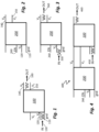
- FIG. 1 shows, conceptually, a level shifter 100.
- the level shifter may generate the voltage level V C linked to the high voltage rail V B , or may be provided with the voltage rail V C from an external circuit.
- FIG. 2 shows a high voltage circuit 200 consistent with one or more embodiments of the present disclosure.
- the high voltage circuit may alternatively be referred to as a multi-voltage-domain circuit, a "floating high voltage level shifter", or a voltage-level setting circuit.
- the high voltage circuit is provided with an input at a reference level which may be for instance GND 0 V, and a low-voltage level V A .
- the high voltage circuit 200 is further provided with a high-voltage rail V B 140.
- the function of the high voltage circuit 200 is to provide a voltage level Vc which is tied to the high voltage rail V B . Operation of the high voltage circuit 200 is controlled by an enable input EN 260.
- the circuit is arranged to generate the voltage V C in case that an enable signal is "on” (which according to one convention may be the case when enable is low or 0). Conversely, when the enable signal is "off” the circuit is disabled and does not generate the voltage V C .
- the high-voltage circuit 200 may have various applications, two of which are shown, schematically, in FIG. 3 and FIG. 4 :
- FIG. 3 illustrates the circuit of FIG. 2 being implemented directly as a level shifter.
- the circuit is provided with a further signal, being an input signal IN 330, in the low-voltage domain, that is to say IN has a value 0 (or ground, 110) in its “low” state and a value V A , 120, in its “high” state.
- IN input signal
- the circuit provides an output OUT 360.
- the enable signal EN 260 is "on"
- the output OUT follows the input signal IN, but translated, or shifted, to the high voltage domain.
- the output OUT may be used as a floating power supply for one or more other circuits, such as but not limited to a conventional level shifter.
- FIG. 4 illustrates the circuit of FIG. 2 implemented as a floating power supply for a conventional level shifter 100.
- the high voltage circuit 200 provides an output voltage V C in response to the enable signal EN 260 being "on".
- the input for the level shifter, IN 430 is then shifted, in voltage, by the level shifter to the high voltage domain to provide output OUT 460, which follows the input 430.
- the output OUT 460 switches between the high voltage rail V B and the voltage level Vc supplied by the high voltage circuit 200.
- High-voltage circuit 500 comprises five main circuit or blocks.
- Voltage-offset circuit (or block) 510 is configured to fix, in operation, the voltage V C , relative to the high voltage power supply rail V B .
- Push-pull circuit (or block) 520 is configured to stabilise the offset voltage provided by voltage-offset circuit 510 circuit block.
- Bias circuit (or block) 530 is configured to provide, under appropriate conditions, a suitable bias current to the push-pull circuit 520.
- High-voltage stand-off circuit (or block) 550 which may alternatively be referred to as a voltage isolation circuit, comprises high-voltage switches, and is configured to provide voltage isolation between the high voltage domain (V C to V B ), and the low voltage domain (GND to V IN ) And finally, pull up circuit (or block) 540 is configured to, in an "off"-state or when VC is not required, reduce or minimise leakage current by ensuring that V C is pulled to the same voltage as the supply rail V B .
- the high-voltage stand-off circuit 550 isolates the high-voltage domain (which includes voltage-offset circuit 510 and pull-up circuit 540) from the low-voltage; in other words the nodes 522 and 524 between the high-voltage stand-off circuit 550 and the voltage-offset circuit 510 are isolated from ground. It further prevents the voltage-offset circuit 510 from operating to control V C .
- a pull up circuit 540 may be provided.
- Pull up circuit 540 may provide one or both of a high-ohmic or capacitive connection between V C and V B , such that, in the absence of active control by the voltage-offset circuit 510, the voltage V C is pulled up, to be equal to the high voltage rail V B . Because the voltage-offset circuit 510 has been disabled, the circuit consumes a very low quiescent current, that is to say when it is not enabled. This may be, for example, of the order of ⁇ 10nA.
- the bias circuit 530 provides a bias current Ib1 to the high-voltage stand-off circuit 550. Current is provided through node 522 to the high-voltage stand-off circuit, and in particular to the push-pull circuit 520. The output of push-pull circuit 520 (at node 526 matches the input current at 522, so a current Ib1 is provided at node 526, and thus to the output V C .
- the voltage offset circuit 510 which is enabled, provides a fixed voltage differential between the high voltage rail V B and the output Vc.
- the voltage-offset circuit 510 defines the voltage at output Vc.
- the current Ib1 at node 522 flows to the voltage rail V B through a voltage-drop circuit 512.
- Voltage-drop circuit 512 may be implemented as a set of M series-connected p-FETs.
- the uppermost p-FET is connected to the high voltage rail V B at its source, and its drain is connected to the next p-FET in the series-connected set.
- the gate of each FET is connected to its drain.
- the uppermost M-1 of the p-FETs comprise the voltage-drop circuit, or block, shown schematically in FIG. 5 as a variable voltage supply 512.
- each p-FET in the series-connect set has its gate coupled to the gate of a corresponding set of (M-1) n-FETs which are series-connected between the high voltage rail V C and the output V B .
- This set of (M -1) n-FETs comprises a variable current source, depicted as 514 in figure 5 .
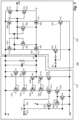
- Figure 6 shows a high voltage circuit 600, being a transistor-level schematic circuit implementation of the circuit shown in block form in FIG. 5 .
- Enable input EN is provided at terminal 602, the ground rail GND at terminal 604, and high-voltage-supply rail V B at terminal 606, and input IN at terminal 608.
- Terminal 612 is provided for receiving a bias current lb.
- a pair of inverters 614, 616 are provided for generating the inverse, ENb, of the enable signal EN.
- Switches 532 and 534 are implemented as an n-FET N5 and p-FET P9 respectively.
- the gate, that is to say the control terminal, of n-FET N5 switch 532 is connected to the inverted enable input, ENb, as is the gate, that is to say the control terminal, of p-FET P9 switch 534.
- the bias circuit 530 is configured as a current mirror comprising two FETs N3 632 and N4 634. When enabled, the current mirror provides a copy of bias input current Ib provided at a terminal 612 to the high-voltage stand-off circuit 550, as mirror current Ib1.
- the high-voltage stand-off circuit 550 is configured as a pair of high-voltage n-FETs NH1 552 and NH2 554.
- high-voltage n-FET and “high-voltage p-FET” refer to FET devices which are able to withstand a significantly higher voltage than used in the logic circuits.
- logic circuits may require, as discussed above approximately 5 V of operation between source and drain.
- high-voltage FETs may be able to withstand 24 V, 48 V 100 V or even 200 V between their source and drain.
- references herein to FETs which are not referred to as high-voltage FETS may be considered to be references to (relatively) low-voltage FETs, that is to say to FETs which may not be able to withstand such high voltages (such as 24 V, 48 V, hundred V or even 200 V between drain and source), without sustaining damage.
- the gates of the n-FETs NH1 552 and NH2 554 are commonly connected to combinatorial logic 670, which may be implemented, as shown, as a single 'AND' gate having inputs connected to the enable EN terminal 602 and the IN terminal 608.
- the EN input may be directly connected to enable terminal 602 or, as shown, through the pair of inverters 614 and 616.
- the skilled person will appreciate that other forms of logic, and/or connection configurations may be used, provided that the gates are high if and only if the enable signal EN is high and the input signal IN is high.
- the source of one of the high-voltage n-FETs, NH1 552, is connected to the bias circuit 530 to receive copy bias currents Ib1; the source of the other n-FET, NH2 554, is connected directly to the ground rail.
- the drains of the n-FETs NH1 552 and NH2 554 are connected to the voltage-offset circuit 510 at nodes 522 and 524 respectively.
- the n-FETs 552 and 554 are high-voltage n-FETs. That is to say, in their off-state, they can withstand the voltage between the high voltage rail VB and ground.
- the voltage-offset circuit 510 comprising the push-pull circuit 520, voltage-drop circuit 512, and current source 514 is, in this implementation, configured as follows.
- the push-pull circuit comprises a pair of p-FETs pH1 622 and pH2 624 having commonly connected gates. The gates are also connected to the drain of pH1 622, such that p-FET P5 626 is diode-connected.
- the p-FETs 622 and 624 are high-voltage p-FETs. That is to say, in their off-state, they can withstand the voltage between the high voltage rail V B and ground.
- the drain of p-FET PH1 622 is connected to node 522 for receiving the copy bias current Ib1 in the case that n-FET NH1 552 is on.
- the drain of p-FET PH2 624 is connected to node 524 and thus connected to the ground rail in the case that the n- FET NH2 554 is on.
- the push-pull circuit further comprises a second pair of FETs, p-FET P5 626 and n-FET N6 628. Again, these FETs have commonly connected gates which are also connected to the drain of p-FET P5 626.
- the drain of p-FET P5 626 is connected to the source of the p-FET PH1 622, and the source of the n-FET N6 628 is connected to the source of the p-FET PH2 624.
- a node 526 between the source of N-FET N6 628 and source of p-FET PH2 624 comprises the output node Vc.
- P-FET P5 626 is further configured as the lowermost of a set of series-connected p-FETs P1 672, P3 676, and P5 626, comprised in the voltage-offset circuit. Excluding the lowermost p-FETs, this set of p-FETs (that is to say, P1 672 and P3 676) comprise the voltage-drop circuit 512. They are series-connected in the sense that the source of each device is connected to the next one up in the series, the source of the uppermost one in the series, in this case P1 672, being connected to the high voltage rail V B . Each of the p-FETs is "diode-connected", that is to say its gate is tied to its drain.
- the voltage at the drain of the lowermost of the set of series-connected p-FETs (in this implementation P1 672, P3 676 and P5 626) is lower than the high-voltage rail voltage V B , by the sum of the gate-source voltages (Vgs) of each of the transistors in the set.
- Vgs gate-source voltages
- the voltage drop circuit comprises a voltage drop of 2 x Vgs. Since the lowermost transistor P5 626 is diode connected, this is also the voltage at the common gates of P5 626 and N6 628.
- V T the voltage difference between the node 513 connecting the voltage-drop circuit 512 to the push-pull circuit 500 and 20 is Vgs + V T .
- V T the voltage difference between the node 513 connecting the voltage-drop circuit 512 to the push-pull circuit 500 and 20 is Vgs + V T .
- the voltage at output node or terminal Vc 526 differs from V B by 3.Vgs + V T .
- V C V B ⁇ M . Vgs + V T .
- the push-pull circuit 520 includes an additional path between the node 513 and the offset-bias voltage output V C . This is the route through P5 626, PH 162, and PH2 624. This results in a voltage drop between 513 and Vc of Vgs + V'gs + V' T , where V'gs is the gate source voltage through the high-voltage p FET pH 162, and V T is the threshold voltage of high-voltage p FET PH2 264.
- Voltage offset circuit 510 further comprises an additional set of series-connected p-type FETs, connected between the high-voltage-supply rail V B and the output node Vc 526, which comprise the current source 514.
- M series-connected p-type FETs
- the uppermost one of the second set, P2 674 has its source connected to the high-voltage rail V B and its drain connected to the next p-FET in the set (in this case P4, 678).
- the lowermost one of the second set, in this case P4 678 has its drain connected to the output V C 526.
- the gates of each the FETs are connected to respective corresponding gate in the first set of series-connected FETs. In operation, these FETs P4 678 and P2 674 act to provide the current requirement during switching and stabilise the voltage V C .
- the pull-up circuit 540 is configured as a resistor R1 642 high-ohmic resistor connected between the high voltage rail V B , and the output node Vc 526, in parallel with a capacitor C1 644 also connected between the high voltage rail V B , and the output node Vc 526.
- the pull-up circuit acts to tie the voltage at output Vc 526 to the high-voltage rail V B .
- FIG. 7 shows a transistor-level circuit diagram, according to one or more other embodiments of the present disclosure.
- the embodiment shown in FIG. 6 broadly corresponds to the diagram shown in FIG. 3
- this transistor level diagram broadly corresponds to the block diagram shown in FIG. 4 .
- the electronic circuit 700 shown in FIG. 7 may be considered to comprise a electronic circuit 770 acting as a stabilised high-voltage-supply for a level shifter 780.
- Vgs is 1.4 V
- V T is typically of the order of 0.1 V
- V C is approximately 5 V lower the V B .
- V C acts as an output from electronic circuit 770 and as a "low" level, in the high-voltage domain, for an output of the level shifter 780 which voltage shifts an input signal (IN) in a low voltage domain (that is to say between the ground and a low voltage such as 5V or similar which corresponds to a "high” value of each of input IN and enable EN), to a high voltage domain (that is to say between V B and Vc.
- a typical value of V B may be 48 V and thus a typical value of V C may be 43 V.
- the level shifter 780 is a conventional level shifter with which the skilled person will be familiar, and thus will only be described in brief.
- the level shifter comprises two pairs of high-voltage FETs.
- a first pair of the high-voltage FETs are n-FETs, NH1 781 and NH2 782, connected to the ground rail and having their gates connected to the input IN and inverted copy of input IN respectively.
- the second pair of the high-voltage FETs are p-FETs, pH1 783 and pH2 784, connected to NH1 and NH2 respectively.
- the common gates of high-voltage p-FETs PH1 783 and PH2 784 are coupled to the drains of cross coupled n-FETs N1a 785 and N2a 786.
- the sources of high-voltage p-FETs PH1 783 and PH2 784 are coupled to respective drains of cross coupled p-FETs P1a 787 and P2 a 788, the sources of which are coupled to the high-voltage-supply rail VB and the gates of which are cross coupled with the gates of n-FETs N1a 785 and N2a 786.
- the commonly coupled gates are connected to the output OUT via a pair of FETs N3a 791, and P3a 792 which operate to invert the signal (relative to the high-voltage bus rail V B and Vc rather than ground and the low voltage input IN, as the skilled person will immediately appreciate).
- the voltage swing (between “high” and “low” values) in the high voltage domain of the level shifter need not correspond to the voltage swing (between “high” and “low” values) in the low-voltage domain.
- the voltage swing in the high voltage domain may typically be set by the difference in voltage between V B and V C , which is determined by the number of p-FETs in the series connected set, together with the number of N-FETs between the further p FET and the offset-bias outputs node Vc.
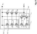
- FIG. 8 this shows a voltage-offset circuit 810.
- the voltage-offset circuit 810 is similar to the voltage-offset circuit 510 shown in FIG. 6 with the exception that in this case M equals four.
- the push-pull circuit comprising pair of p-FETs pH1 622 and pH2 624 having commonly connected gates, and second pair of FETs, p-FET P5 626 and n-FET N6 628, is the same as that shown in FIG. 6 .
- P-FET P5 626 is further configured as the lowermost of a set of series-connected p-FETs P11 871, P1 672, P3 676, and P5 626, comprised in the voltage-offset circuit, and in this case P11 871 is connected to the high voltage rail V B .
- Each of the p-FETs are "diode-connected", that is to say its gate is tied to its drain.
- this voltage-offset circuit includes a voltage-drop circuit 812 comprising the three p-FETs P11 871, P1 672 and P3 676.
- the voltage at the drain of the lowermost of the set of series-connected p-FETs (P11 871 P1 672, P3 676 and P5 626) is lower than the high-voltage rail voltage V B , by the sum of the gate-source voltages (Vgs) of each of the transistors in the set.
- Vgs gate-source voltages
- the voltage at the drain of P5 626 is 4 x Vgs. Since the lowermost transistor P5 626 is diode connected, this is also the voltage at the common gates of P5 626 and N6 628.
- the voltage between the gate and source of N6 is its threshold voltage, V T . So the voltage at output node V C 526 differs from V B by 4.Vgs + V T .
- the additional set of series-connected p-type FETs connected between the high-voltage-supply rail V B and the output node Vc 526 comprises three p-FETs. P12 873, P2 674 and P4 678, having their gates connected to the gates of P11 871, P1 672 and P3 676 respectively.
- FIG. 9 shows a voltage-offset circuit 910.
- the voltage offset circuit 910 is similar to the voltage-offset circuit 810 shown in FIG. 8 with the exception that in this case the push-pull circuit, 920, includes a second n-FET N6' 928 between the, or first, n-FET P6 628 and offset bias node 526.
- a gate of the first n-FET is connected to the gate of the further p-FET
- the drain of the first n-FET is connected to a gate of the second n-FET
- the drain of the second n-FET is connected to the offset-bias output terminal
- the source of each of the first and second n-FET is connected to the high-voltage-supply terminal.
- V C V B ⁇ M . Vgs + P . V T . ,
- (M-1) is the number of series connected p-FETs in the voltage offset circuit 512
- P is the number of n-FETs in the path between the further p-FET P5 626 and the offset bias output terminal, that is to say, the output node V C .
- the high voltage circuit can provide an output VC which is very stable with respect to, and follows variations in, PVT (process voltage and temperature.
- the design may enable the voltage offset to follow the sum of Vgs of the low voltage FETs, and in turn, Vgs is proportional to V T + Vds, where Vds is the drain source voltage.
- bias voltage I b is kept constant, Vds is almost constant, and V T changes with PVT.
- high voltage circuits may have relatively low power consumption (typically of the order of ⁇ 100nA) compared with conventional circuits and may be able to operate at relatively high frequencies (such as up to10Mhz) With respect to conventional circuits.
Landscapes
- Engineering & Computer Science (AREA)
- Computer Hardware Design (AREA)
- Physics & Mathematics (AREA)
- Computing Systems (AREA)
- General Engineering & Computer Science (AREA)
- Mathematical Physics (AREA)
- Logic Circuits (AREA)
Priority Applications (1)
| Application Number | Priority Date | Filing Date | Title |
|---|---|---|---|
| US18/515,621 US12463647B2 (en) | 2022-11-24 | 2023-11-21 | Level shifter and multi-voltage-domain circuits |
Applications Claiming Priority (1)
| Application Number | Priority Date | Filing Date | Title |
|---|---|---|---|
| IN202221067743 | 2022-11-24 |
Publications (1)
| Publication Number | Publication Date |
|---|---|
| EP4391384A1 true EP4391384A1 (de) | 2024-06-26 |
Family
ID=86604944
Family Applications (1)
| Application Number | Title | Priority Date | Filing Date |
|---|---|---|---|
| EP23175334.4A Pending EP4391384A1 (de) | 2022-11-24 | 2023-05-25 | Pegelschieber und schaltungen mit mehreren spannungsdomänen |
Country Status (2)
| Country | Link |
|---|---|
| EP (1) | EP4391384A1 (de) |
| CN (1) | CN118074704A (de) |
Citations (2)
| Publication number | Priority date | Publication date | Assignee | Title |
|---|---|---|---|---|
| US20180138898A1 (en) * | 2016-11-15 | 2018-05-17 | Stmicroelectronics, Inc. | Low output impedance, high speed and high voltage generator for use in driving a capacitive load |
| US10840907B1 (en) * | 2019-11-19 | 2020-11-17 | Honeywell International Inc. | Source-coupled logic with reference controlled inputs |
-
2023
- 2023-05-25 EP EP23175334.4A patent/EP4391384A1/de active Pending
- 2023-11-07 CN CN202311470170.1A patent/CN118074704A/zh active Pending
Patent Citations (2)
| Publication number | Priority date | Publication date | Assignee | Title |
|---|---|---|---|---|
| US20180138898A1 (en) * | 2016-11-15 | 2018-05-17 | Stmicroelectronics, Inc. | Low output impedance, high speed and high voltage generator for use in driving a capacitive load |
| US10840907B1 (en) * | 2019-11-19 | 2020-11-17 | Honeywell International Inc. | Source-coupled logic with reference controlled inputs |
Also Published As
| Publication number | Publication date |
|---|---|
| CN118074704A (zh) | 2024-05-24 |
Similar Documents
| Publication | Publication Date | Title |
|---|---|---|
| US5113097A (en) | CMOS level shifter circuit | |
| US5144167A (en) | Zero power, high impedance TTL-to-CMOS converter | |
| US5578941A (en) | Voltage compensating CMOS input buffer circuit | |
| US7176741B2 (en) | Level shift circuit | |
| US7123055B1 (en) | Impedance-matched output driver circuits having coarse and fine tuning control | |
| US7804350B1 (en) | Level shifting using cross-coupled cascode transistors | |
| WO2012151177A1 (en) | System and method for level-shifting voltage signals using a dynamic level-shifting architecture | |
| GB2360405A (en) | A common-gate level-shifter exhibiting a high input impedance when disabled | |
| CN110875736B (zh) | 低功耗负压电平移位器 | |
| GB2347567A (en) | CMOS level shifters and sense amplifiers | |
| US5973530A (en) | Low power, high voltage-tolerant bus holder circuit in low voltage technology | |
| US12463647B2 (en) | Level shifter and multi-voltage-domain circuits | |
| EP4372992A1 (de) | Kaskodentransistorschalter | |
| US7746145B2 (en) | Level shift circuit capable of preventing occurrence of malfunction when low power supply fluctuates, and semiconductor integrated circuit including the circuit | |
| US7816969B2 (en) | Level shifter circuit | |
| EP0810732A2 (de) | Differenzsignal-Generatorschaltung mit einer Schaltung zur Stromspitzenunterdrückung | |
| US6624678B1 (en) | Schmitt trigger device with disable | |
| EP4391384A1 (de) | Pegelschieber und schaltungen mit mehreren spannungsdomänen | |
| US7400171B1 (en) | Electronic switch having extended voltage range | |
| US12381560B2 (en) | Semiconductor device including a level shifter and method of mitigating a delay between input and output signals | |
| EP0782269A2 (de) | Integrierte Halbleiterschaltung | |
| KR20020082232A (ko) | 매우 낮은 파워 서플라이용 레벨 시프터 | |
| US12212320B2 (en) | Level shifter circuit, corresponding device and method | |
| US6559704B1 (en) | Inverting level shifter with start-up circuit | |
| US12199606B2 (en) | Level shifter with expanded voltage range |
Legal Events
| Date | Code | Title | Description |
|---|---|---|---|
| PUAI | Public reference made under article 153(3) epc to a published international application that has entered the european phase |
Free format text: ORIGINAL CODE: 0009012 |
|
| STAA | Information on the status of an ep patent application or granted ep patent |
Free format text: STATUS: THE APPLICATION HAS BEEN PUBLISHED |
|
| AK | Designated contracting states |
Kind code of ref document: A1 Designated state(s): AL AT BE BG CH CY CZ DE DK EE ES FI FR GB GR HR HU IE IS IT LI LT LU LV MC ME MK MT NL NO PL PT RO RS SE SI SK SM TR |
|
| STAA | Information on the status of an ep patent application or granted ep patent |
Free format text: STATUS: REQUEST FOR EXAMINATION WAS MADE |
|
| 17P | Request for examination filed |
Effective date: 20250102 |