EP4391282A1 - Protective device for preventing reverse connection - Google Patents
Protective device for preventing reverse connection Download PDFInfo
- Publication number
- EP4391282A1 EP4391282A1 EP22887376.6A EP22887376A EP4391282A1 EP 4391282 A1 EP4391282 A1 EP 4391282A1 EP 22887376 A EP22887376 A EP 22887376A EP 4391282 A1 EP4391282 A1 EP 4391282A1
- Authority
- EP
- European Patent Office
- Prior art keywords
- node
- switch
- relay
- input terminal
- output terminal
- Prior art date
- Legal status (The legal status is an assumption and is not a legal conclusion. Google has not performed a legal analysis and makes no representation as to the accuracy of the status listed.)
- Granted
Links
Images



Classifications
-
- H—ELECTRICITY
- H02—GENERATION; CONVERSION OR DISTRIBUTION OF ELECTRIC POWER
- H02H—EMERGENCY PROTECTIVE CIRCUIT ARRANGEMENTS
- H02H11/00—Emergency protective circuit arrangements for preventing the switching-on in case an undesired electric working condition might result
- H02H11/002—Emergency protective circuit arrangements for preventing the switching-on in case an undesired electric working condition might result in case of inverted polarity or connection; with switching for obtaining correct connection
-
- H—ELECTRICITY
- H02—GENERATION; CONVERSION OR DISTRIBUTION OF ELECTRIC POWER
- H02H—EMERGENCY PROTECTIVE CIRCUIT ARRANGEMENTS
- H02H3/00—Emergency protective circuit arrangements for automatic disconnection directly responsive to an undesired change from normal electric working condition with or without subsequent reconnection ; integrated protection
- H02H3/18—Emergency protective circuit arrangements for automatic disconnection directly responsive to an undesired change from normal electric working condition with or without subsequent reconnection ; integrated protection responsive to reversal of direct current
-
- H—ELECTRICITY
- H02—GENERATION; CONVERSION OR DISTRIBUTION OF ELECTRIC POWER
- H02J—ELECTRIC POWER NETWORKS; CIRCUIT ARRANGEMENTS OR SYSTEMS FOR SUPPLYING OR DISTRIBUTING ELECTRIC POWER; SYSTEMS FOR STORING ELECTRIC ENERGY
- H02J7/00—Circuit arrangements for charging or discharging batteries or for supplying loads from batteries
-
- H—ELECTRICITY
- H02—GENERATION; CONVERSION OR DISTRIBUTION OF ELECTRIC POWER
- H02J—ELECTRIC POWER NETWORKS; CIRCUIT ARRANGEMENTS OR SYSTEMS FOR SUPPLYING OR DISTRIBUTING ELECTRIC POWER; SYSTEMS FOR STORING ELECTRIC ENERGY
- H02J7/00—Circuit arrangements for charging or discharging batteries or for supplying loads from batteries
- H02J7/60—Circuit arrangements for charging or discharging batteries or for supplying loads from batteries including safety or protection arrangements
-
- H—ELECTRICITY
- H02—GENERATION; CONVERSION OR DISTRIBUTION OF ELECTRIC POWER
- H02J—ELECTRIC POWER NETWORKS; CIRCUIT ARRANGEMENTS OR SYSTEMS FOR SUPPLYING OR DISTRIBUTING ELECTRIC POWER; SYSTEMS FOR STORING ELECTRIC ENERGY
- H02J7/00—Circuit arrangements for charging or discharging batteries or for supplying loads from batteries
- H02J7/60—Circuit arrangements for charging or discharging batteries or for supplying loads from batteries including safety or protection arrangements
- H02J7/62—Circuit arrangements for charging or discharging batteries or for supplying loads from batteries including safety or protection arrangements against overcurrent
-
- H—ELECTRICITY
- H02—GENERATION; CONVERSION OR DISTRIBUTION OF ELECTRIC POWER
- H02J—ELECTRIC POWER NETWORKS; CIRCUIT ARRANGEMENTS OR SYSTEMS FOR SUPPLYING OR DISTRIBUTING ELECTRIC POWER; SYSTEMS FOR STORING ELECTRIC ENERGY
- H02J7/00—Circuit arrangements for charging or discharging batteries or for supplying loads from batteries
- H02J7/60—Circuit arrangements for charging or discharging batteries or for supplying loads from batteries including safety or protection arrangements
- H02J7/663—Circuit arrangements for charging or discharging batteries or for supplying loads from batteries including safety or protection arrangements using battery or load disconnect circuits
-
- H—ELECTRICITY
- H02—GENERATION; CONVERSION OR DISTRIBUTION OF ELECTRIC POWER
- H02J—ELECTRIC POWER NETWORKS; CIRCUIT ARRANGEMENTS OR SYSTEMS FOR SUPPLYING OR DISTRIBUTING ELECTRIC POWER; SYSTEMS FOR STORING ELECTRIC ENERGY
- H02J7/00—Circuit arrangements for charging or discharging batteries or for supplying loads from batteries
- H02J7/60—Circuit arrangements for charging or discharging batteries or for supplying loads from batteries including safety or protection arrangements
- H02J7/68—Circuit arrangements for charging or discharging batteries or for supplying loads from batteries including safety or protection arrangements using circuits for correcting or protecting against reverse-polarity
-
- H—ELECTRICITY
- H02—GENERATION; CONVERSION OR DISTRIBUTION OF ELECTRIC POWER
- H02H—EMERGENCY PROTECTIVE CIRCUIT ARRANGEMENTS
- H02H7/00—Emergency protective circuit arrangements specially adapted for specific types of electric machines or apparatus or for sectionalised protection of cable or line systems, and effecting automatic switching in the event of an undesired change from normal working conditions
- H02H7/18—Emergency protective circuit arrangements specially adapted for specific types of electric machines or apparatus or for sectionalised protection of cable or line systems, and effecting automatic switching in the event of an undesired change from normal working conditions for batteries; for accumulators
-
- Y—GENERAL TAGGING OF NEW TECHNOLOGICAL DEVELOPMENTS; GENERAL TAGGING OF CROSS-SECTIONAL TECHNOLOGIES SPANNING OVER SEVERAL SECTIONS OF THE IPC; TECHNICAL SUBJECTS COVERED BY FORMER USPC CROSS-REFERENCE ART COLLECTIONS [XRACs] AND DIGESTS
- Y10—TECHNICAL SUBJECTS COVERED BY FORMER USPC
- Y10S—TECHNICAL SUBJECTS COVERED BY FORMER USPC CROSS-REFERENCE ART COLLECTIONS [XRACs] AND DIGESTS
- Y10S320/00—Electricity: battery or capacitor charging or discharging
- Y10S320/18—Indicator or display
Definitions
- the disclosure relates to a protection device for preventing reverse connection.
- An energy storage system that stores power and provides the stored power is being used in various fields.
- the ESS may be used to store power overproduced in a power plant and provide the power when a temporary power shortage occurs.
- the ESS may be manufactured in a small size to be used in buildings, factories, homes, etc. in case of a power failure or for peak power reduction.
- the ESS may be used to store power produced using new renewable energy and use the stored power in a desired time zone.
- a rechargeable battery is used for the ESS.
- the rechargeable battery may be used as an energy source of various types of external devices such as an electronic device and a moving means, as well as the ESS.
- An electronic device such as a battery management system, is used for protection or management of a battery, together with the battery.
- a direct-current (DC) voltage is applied to operate the electronic device.
- a power source that applies a DC voltage is connected to a power input terminal of the electronic device.
- a reverse connection causing a positive terminal of the power source to be connected to a negative terminal of the power input terminal may occur.
- a reverse voltage may be applied to the electronic device, thus causing a malfunction of the electronic device.
- the present invention has been made in an effort to provide a protection device having advantages of preventing reverse connection of a direct-current (DC) power source.
- DC direct-current
- An exemplary embodiment of the present invention provides a protection device of an electronic device to which power is supplied from a direct-current power source that includes a positive wiring and a negative wiring.
- the protection device includes a first switch, a second switch, a first relay, and a second relay.
- the first switch includes an input terminal to which the positive wiring or the negative wiring is connected, a first output terminal connected to a first node, and a second output terminal connected to a second node.
- the second switch includes an input terminal to which the positive wiring or the negative wiring is connected, a first output terminal connected to a third node, and a second output terminal connected to a fourth node.
- the first relay includes a first relay switch and a first driver.
- the first relay switch includes a first terminal connected to the first node and a second terminal connected to a positive input terminal of the electronic device.
- the first driver is configured to drive the first relay switch, and includes an input terminal connected to the first node.
- the second relay includes a second relay switch and a second driver.
- the second relay switch includes a first terminal connected to a negative input terminal of the electronic device and a second terminal connected to the third node.
- the second driver is configured to drive the second relay switch, and includes an input terminal connected to an output terminal of the first driver and an output terminal connected to the third node.
- the protection device may further include a diode configured to block current flowing from the third node to the first node through the second driver and the first driver.
- the protection device may further include an indication element connected between the first node and the third node and configured to perform an indication operation when current flows from the third node to the first node.
- the indication element may include a light-emitting diode configured to emit light when current flows from the third node to the first node.
- the protection device may further include an indication element connected between the second node and the fourth node and configured to perform an indication operation when current flows from the fourth node to the second node.
- the indication element may include a light-emitting diode configured to emit light when current flows from the fourth node to the second node.
- the electronic device may include an electronic device configured to manage a battery.
- the protection device includes a first switch, a second switch, a first relay, a second relay, and an indication element.
- the first switch includes an input terminal to which the positive wiring or the negative wiring is connected, a first output terminal connected to a first node, and a second output terminal connected to a second node.
- the second switch includes an input terminal to which the positive wiring or the negative wiring is connected, a first output terminal connected to a third node, and a second output terminal connected to a fourth node.
- the first relay is connected between the first node and a positive input terminal of the electronic device.
- the second relay is connected between the third node and a negative input terminal of the electronic device.
- the indication element is connected between the second node and the fourth node, and configured to perform an indication operation when the negative wiring is connected to the input terminal of the first switch and the positive wiring is connected to the input terminal of the second switch in a state in which the first switch is switched to the second output terminal and the second switch is switched to the second output terminal.
- the indication element may include a light-emitting diode configured to emit light when current flows from the fourth node to the second node.
- the first relay and the second relay may be turned on when the positive wiring is connected to the input terminal of the first switch and the negative wiring is connected to the input terminal of the second switch in a state in which the first switch is switched to the first output terminal thereof and the second switch is switched to the first output terminal thereof.
- the first relay and the second relay may be turned off when the negative wiring is connected to the input terminal of the first switch and the positive wiring is connected to the input terminal of the second switch in a state in which the first switch is switched to the first output terminal thereof and the second switch is switched to the first output terminal thereof.
- the electronic device may include an electronic device configured to manage a battery.
- Yet another embodiment of the present invention provides a protection device of an electronic device to which power is supplied from a direct-current power source that includes a positive wiring and a negative wiring.
- the protection device includes a first switch, a second switch, a first relay, a second relay, and an indication element.
- the first switch includes an input terminal to which the positive wiring or the negative wiring is connected, a first output terminal connected to a first node, and a second output terminal connected to a second node.
- the second switch includes an input terminal to which the positive wiring or the negative wiring is connected, a first output terminal connected to a third node, and a second output terminal connected to a fourth node.
- the first relay is connected between the first node and a positive input terminal of the electronic device.
- the second relay is connected between the third node and a negative input terminal of the electronic device.
- the indication element is connected between the first node and the third node, and configured to perform an indication operation when the negative wiring is connected to the input terminal of the first switch and the positive wiring is connected to the input terminal of the second switch in a state in which the first switch is switched to the first output terminal thereof and the second switch is switched to the first output terminal thereof.
- the indication element may include a light-emitting diode configured to emit light when current flows from the third node to the first node.
- the first relay and the second relay may be turned on when the positive wiring is connected to the input terminal of the first switch and the negative wiring is connected to the input terminal of the second switch in a state in which the first switch is switched to the first output terminal and the second switch is switched to the first output terminal.
- the first relay and the second relay may be turned off when the negative wiring is connected to the input terminal of the first switch and the positive wiring is connected to the input terminal of the second switch in a state in which the first switch is switched to the first output terminal and the second switch is switched to the first output terminal.
- the first relay and the second relay may be turned off in a state in which the first switch is switched to the second output terminal and the second switch is switched to the second output terminal.
- the electronic device may include an electronic device configured to manage a battery.
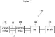
- FIG. 1 is a diagram illustrating an example of a battery device according to an exemplary embodiment.
- a battery device 100 includes a battery 110, a battery management system 120, and a protection device 130.
- the battery 110 is a rechargeable secondary battery.
- the battery 110 may be a lithium battery, such as a lithium ion battery or a lithium ion polymer battery, or a nickel battery, such as a nickel-cadmium (NiCd) battery or a nickel hydrogen (NiMH) battery.
- the battery 110 may be a single battery cell, a battery module in which an assembly of multiple battery cells or multiple assemblies of batteries are connected in series or parallel, a battery pack (or battery rack) in which multiple battery modules are connected in series or parallel, or a device in which multiple battery packs (battery racks) are connected in series or parallel.
- the battery management system 120 is an electronic device that manages the battery 110, and protects the battery 110 or monitors information of or a state of the battery 110.
- the battery management system 120 may be referred to as a battery protection unit (BPU).
- BPU battery protection unit
- the battery management system 120 operates by receiving a direct current (DC) voltage from a DC power source 10.
- the DC power source 10 includes a positive terminal and a negative terminal, a positive wiring 11 is connected to the positive terminal, and a negative wiring 12 is connected to the negative terminal.
- the DC power source 10 may supply power through the positive wiring 11 and the negative wiring 12.
- the battery device 100 may be an energy management system.
- the DC power source 10 may include a power converter, e.g., a switching mode power supply (SMPS), which converts power from an external alternating current (AC) power source into a DC voltage.
- SMPS switching mode power supply
- the protection device 130 is connected between the DC power source 10 and a power input terminal of the battery management system 120.
- the protection device 130 performs a protection function to connect the positive wiring 11 of the DC power source 10 to a positive input terminal of the battery management system 120 and the negative wiring 12 of the DC power source 10 to a negative input terminal of the battery management system 120.
- the protection device 130 may disconnect the DC power source 10 and the power input terminal of the battery management system 120 from each other when the positive wiring 11 of the DC power source 10 is connected to the negative input terminal of the battery management system 120.
- the protection device 130 may transmit power from the DC power source 10 to the battery management system 120, when the positive wiring 11 of the DC power source 10 is connected to the positive input terminal of the battery management system 120 and the negative wiring 12 of the DC power source 10 is connected to the negative input terminal of the battery management system 120.
- FIG. 2 is a diagram illustrating an example of a protection device according to an exemplary embodiment.
- the protection device includes switches S1, S2, S3, and S4.
- the switch S1 includes an input terminal P1 and first and second output terminals T11 and T12
- the switch S2 includes an input terminal P2 and first and second output terminals T21 and T22.
- the input terminals P1 and P2 of the switches S1 and S2 correspond to input terminals of the protection device.
- each of the switches S1 and S2 may be a single pole double throw (SPDT) switch.
- the two switches S1 and S2 may be formed as one double pole double throw (DPDT) switch.
- the switch S1 may connect the input terminal P1 and the first output terminal T11 when turned on, and connect the input terminal P1 and the second output terminal T12 when turned off.
- the switch S2 may connect the input terminal P2 and the first output terminal T21 when turned on, and connect the input terminal P2 and the second output terminal T22 when turned off.
- the second output terminal T12 of the switch S1 is connected to one node (e.g., a "second node") N2, and the second output terminal T22 of the switch S2 is connected to another node (e.g., a "fourth node”) N4. That is, the second output terminal T12 of the switch S1 and the second output terminal T22 of the switch S2 are connected to each other.
- the switch S3 includes an input terminal (or “first terminal”) P3 and an output terminal (or “second terminal”) T3 and the switch S4 includes an input terminal (or “first terminal”) P4 and an output terminal (or “second terminal”) T4.
- each of the switches S3 and S4 may be a relay.
- the switches S3 and S4 will be hereinafter referred to as relays.
- the relay S3 includes a relay switch S3a and a relay driver S3b, and the relay switch S3a may be turned on when current flows through the relay driver S3b.
- the relay S4 includes a relay switch S4a and a relay driver S4b, and the relay switch S4a may be turned on when current flows through the relay driver S4b.
- the relay drivers S3b and S4b may be light-emitting diodes (LEDs), and the relay switches S3a and S4a may be metal oxide semiconductor field-effect transistors (MOSFETs).
- the relays S3 and S4 may be, for example, photo-MOS relays.
- the input terminal P1 of the switch S1 and the input terminal P2 of the switch S2 are connected to a positive wiring 21 and a negative wiring 22 of a DC power source 20, respectively.
- the first output terminal T11 of the switch S1 is connected to one node (or “first node") N1, and the input terminal (or “first terminal") P3 of the relay switch S3a is connected to the node N1.
- the first output terminal T21 of the switch S2 is connected to another node (or "third node”) N3, and an output terminal (or "second terminal”) of the relay switch S4a is connected to the node N3.
- the first output terminal T11 of the switch S1 is connected to the input terminal P3 of the relay switch S3a, and the first output terminal T21 of the switch S2 is connected to the output terminal T4 of the relay switch S4a.
- the output terminal (or “second terminal”) T3 of the relay switch S3a and the input terminal (or “first terminal") P4 of the relay switch S4a are connected to a product 23 to which power is supplied from the DC power source 20.
- the product 23 may include an electronic device such as a battery management system (e.g., the battery management system 120 of FIG. 1 ).
- the output terminal T3 of the relay switch S3a is connected to a positive input terminal IN(+) of the product 23, and the input terminal P4 of the relay switch S4a is connected to a negative input terminal IN(-) of the product 23. Therefore, the DC power source 20 may be connected to the protection device in a forward direction, when the positive wiring 21 of the DC power source 20 is connected to the input terminal P1 of the switch S1 and the negative wiring 22 of the DC power source 20 is connected to the input terminal P2 of the switch S2.
- An input terminal (or "first terminal") of the relay driver S3b is connected to the node N1
- an output terminal (or “second terminal”) of the relay driver S3b is connected to an input terminal (or "first terminal") of the relay driver S4b
- an output terminal (or “second terminal") of the relay driver S4b is connected to the node N3. Accordingly, the input terminal of the relay driver S3b is connected to the first output terminal T11 of the switch S1, and the output terminal of the relay driver S4b is connected to the first output terminal T21 of the switch S2.
- a diode D1 may be formed between the nodes N1 and N3 to prevent reverse current from flowing in a path formed by the relay drivers S3b and S4b.
- the diode D1 may allow current to flow from the node N1 to the node N3 through the relay drivers S3b and S4b, and prevent current from flowing from the node N3 to the node N1 through the relay drivers S3b and S4b.
- an anode of the diode D1 may be connected to the output terminal of the relay driver S3b, and a cathode of the diode D1 may be connected to the input terminal of the relay driver S4b.
- resistors R2 and R3 may be formed in a path between the nodes N1 and N3 formed through the relay drivers S3b and S4b.
- an indication element LD1 may be connected between the nodes N1 and N3.
- a resistor R1 may be further connected between the nodes N1 and N3.
- the resistor R1 and the indication element LD1 may be connected in series between the nodes N1 and N3.
- the indication element LD1 may perform an indication operation when current flows from the node N3 to the node N1.
- the indication element LD1 may be a light-emitting diode that emits light to perform the indication operation when current flows therethrough.
- the cathode of the light-emitting diode LD1 may be connected to the node N1 and the anode of the light-emitting diode LD1 may be connected to the node N3.
- an indication element LD2 may be connected between the nodes N2 and N4.
- a resistor R4 may be further connected between the nodes N2 and N4.
- the resistor R4 and the indication element LD2 may be connected in series between the nodes N2 and N2.
- the indication element LD2 may perform the indication operation when a current flows from the node N4 to the node N2.
- the indication element LD2 may be a light-emitting diode that emits light to perform the indication operation when current flows therethrough.
- a cathode of the light-emitting diode LD2 may be connected to the node N2 and an anode of the light-emitting diode LD2 may be connected to the node N4.
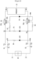
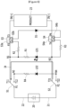
- FIGS. 3 and 5 are diagrams illustrating examples of an operation of a protection device in a forward connection state according to exemplary embodiments.
- FIGS. 4 and 6 are diagrams illustrating examples of an operation of a protection device in a reverse connection state according to exemplary embodiments.
- a DC power source 20 may be connected to an input terminal of the protection device, i.e., input terminals P1 and P2 of switches S1 and S2, in a state in which the switches S1 and S2 are turned off. That is, the DC power source 20 may be connected to the input terminals P1 and P2 of the switches S1 and S2 in a state in which the switch S1 is switched to a second output terminal T12 (or a node N2) and the switch S2 is switched to a second output terminal T22 (or a node N4).
- relays S3 and S4 are in a turned-off state because current is not supplied to relay drivers S3b and S4b.
- a positive wiring 21 of the DC power source 20 is connected to the input terminal P1 of the switch S1 and a negative wiring 22 of the DC power source 20 is connected to the input terminal P2 of the switch S2.
- current does not flow through an indication element LD2 and thus an indication element LD2 does not perform the indication operation.
- the indication element e.g., a light-emitting diode, LD2 does not emit light.
- the indication element LD2 performs an indication operation. For example, the current I1 flows through the indication element (e.g., a light emitting diode) LD2 and thus the indication element LD2 emits light.
- the indication element e.g., a light emitting diode
- whether the DC power source 20 is connected to the protection device in the forward direction or the reverse direction may be identified according to whether the indication element LD2 performs the indication operation.
- the indication element LD2 indicates a reverse connection
- a user may connect the DC power source 20 to the protection device in the forward direction by connecting the wirings 21 and 22 to the protection device in an opposite direction.
- a DC power source 20 may be connected to the input terminal of the protection device, i.e., the input terminals P1 and P2 of the switches S1 and S2, in a state in which the switches S1 and S2 are turned on. That is, the DC power source 20 may be connected to the input terminals P1 and P2 of the switches S1 and S2 in a state in which the switch S1 is switched to a first output terminal (or a node N1) and the switch S2 is switched to a second output terminal (or a node N3).
- the protection device may block a reverse voltage of the DC power source 20 from being applied to the product 23.
- current I4 flows from the node N3 to the node N1 through the indication element LD1 due to the DC power source 20 connected in the reverse direction. Because the current I3 flows through the indication element LD1, the indication element LD1 performs the indication operation. For example, the current I3 flows through the indication element (e.g., a light emitting diode) LD1 and thus the indication element LD1 emits light.
- the indication element e.g., a light emitting diode
- whether the DC power source 20 is connected to the protection device in the forward direction or the reverse direction may be identified according to whether the indication element LD1 performs the indication operation.
- the indication element LD2 indicates a reverse connection
- a user may connect the DC power source 20 to the protection device in the forward direction by connecting the wirings 21 and 22 to the protection device in an opposite direction.
- power from the DC power source 20 may be blocked from being supplied to the product 23.
Landscapes
- Engineering & Computer Science (AREA)
- Power Engineering (AREA)
- Charge And Discharge Circuits For Batteries Or The Like (AREA)
- Emergency Protection Circuit Devices (AREA)
Abstract
Description
- This application claims priority to and the benefit of
Korean Patent Application No. 10-2021-0143322 filed in the Korean Intellectual Property Office on October 26, 2021 - The disclosure relates to a protection device for preventing reverse connection.
- An energy storage system (ESS) that stores power and provides the stored power is being used in various fields. For example, the ESS may be used to store power overproduced in a power plant and provide the power when a temporary power shortage occurs. The ESS may be manufactured in a small size to be used in buildings, factories, homes, etc. in case of a power failure or for peak power reduction. In addition, the ESS may be used to store power produced using new renewable energy and use the stored power in a desired time zone.
- A rechargeable battery is used for the ESS. The rechargeable battery may be used as an energy source of various types of external devices such as an electronic device and a moving means, as well as the ESS.
- An electronic device, such as a battery management system, is used for protection or management of a battery, together with the battery. A direct-current (DC) voltage is applied to operate the electronic device. To this end, in general, a power source that applies a DC voltage is connected to a power input terminal of the electronic device. However, when the power source is connected to the power input terminal of the electronic device, a reverse connection causing a positive terminal of the power source to be connected to a negative terminal of the power input terminal may occur. In this case, a reverse voltage may be applied to the electronic device, thus causing a malfunction of the electronic device.
- The present invention has been made in an effort to provide a protection device having advantages of preventing reverse connection of a direct-current (DC) power source.
- An exemplary embodiment of the present invention provides a protection device of an electronic device to which power is supplied from a direct-current power source that includes a positive wiring and a negative wiring. The protection device includes a first switch, a second switch, a first relay, and a second relay. The first switch includes an input terminal to which the positive wiring or the negative wiring is connected, a first output terminal connected to a first node, and a second output terminal connected to a second node. The second switch includes an input terminal to which the positive wiring or the negative wiring is connected, a first output terminal connected to a third node, and a second output terminal connected to a fourth node. The first relay includes a first relay switch and a first driver. The first relay switch includes a first terminal connected to the first node and a second terminal connected to a positive input terminal of the electronic device. The first driver is configured to drive the first relay switch, and includes an input terminal connected to the first node. The second relay includes a second relay switch and a second driver. The second relay switch includes a first terminal connected to a negative input terminal of the electronic device and a second terminal connected to the third node. The second driver is configured to drive the second relay switch, and includes an input terminal connected to an output terminal of the first driver and an output terminal connected to the third node.
- According to an embodiment of the present invention, the protection device may further include a diode configured to block current flowing from the third node to the first node through the second driver and the first driver.
- According to an embodiment of the present invention, the protection device may further include an indication element connected between the first node and the third node and configured to perform an indication operation when current flows from the third node to the first node.
- According to an embodiment of the present invention, the indication element may include a light-emitting diode configured to emit light when current flows from the third node to the first node.
- According to an embodiment of the present invention, the protection device may further include an indication element connected between the second node and the fourth node and configured to perform an indication operation when current flows from the fourth node to the second node.
- According to an embodiment of the present invention, the indication element may include a light-emitting diode configured to emit light when current flows from the fourth node to the second node.
- According to an embodiment of the present invention, the electronic device may include an electronic device configured to manage a battery.
- Another embodiment of the present invention provides a protection device of an electronic device to which power is supplied from a direct-current power source that includes a positive wiring and a negative wiring. The protection device includes a first switch, a second switch, a first relay, a second relay, and an indication element. The first switch includes an input terminal to which the positive wiring or the negative wiring is connected, a first output terminal connected to a first node, and a second output terminal connected to a second node. The second switch includes an input terminal to which the positive wiring or the negative wiring is connected, a first output terminal connected to a third node, and a second output terminal connected to a fourth node. The first relay is connected between the first node and a positive input terminal of the electronic device. The second relay is connected between the third node and a negative input terminal of the electronic device. The indication element is connected between the second node and the fourth node, and configured to perform an indication operation when the negative wiring is connected to the input terminal of the first switch and the positive wiring is connected to the input terminal of the second switch in a state in which the first switch is switched to the second output terminal and the second switch is switched to the second output terminal.
- According to an embodiment of the present invention, the indication element may include a light-emitting diode configured to emit light when current flows from the fourth node to the second node.
- According to an embodiment of the present invention, the first relay and the second relay may be turned on when the positive wiring is connected to the input terminal of the first switch and the negative wiring is connected to the input terminal of the second switch in a state in which the first switch is switched to the first output terminal thereof and the second switch is switched to the first output terminal thereof.
- According to an embodiment of the present invention, the first relay and the second relay may be turned off when the negative wiring is connected to the input terminal of the first switch and the positive wiring is connected to the input terminal of the second switch in a state in which the first switch is switched to the first output terminal thereof and the second switch is switched to the first output terminal thereof.
- According to an embodiment of the present invention, the electronic device may include an electronic device configured to manage a battery.
- Yet another embodiment of the present invention provides a protection device of an electronic device to which power is supplied from a direct-current power source that includes a positive wiring and a negative wiring. The protection device includes a first switch, a second switch, a first relay, a second relay, and an indication element. The first switch includes an input terminal to which the positive wiring or the negative wiring is connected, a first output terminal connected to a first node, and a second output terminal connected to a second node. The second switch includes an input terminal to which the positive wiring or the negative wiring is connected, a first output terminal connected to a third node, and a second output terminal connected to a fourth node. The first relay is connected between the first node and a positive input terminal of the electronic device. The second relay is connected between the third node and a negative input terminal of the electronic device. The indication element is connected between the first node and the third node, and configured to perform an indication operation when the negative wiring is connected to the input terminal of the first switch and the positive wiring is connected to the input terminal of the second switch in a state in which the first switch is switched to the first output terminal thereof and the second switch is switched to the first output terminal thereof.
- According to an embodiment of the present invention, the indication element may include a light-emitting diode configured to emit light when current flows from the third node to the first node.
- According to an embodiment of the present invention, the first relay and the second relay may be turned on when the positive wiring is connected to the input terminal of the first switch and the negative wiring is connected to the input terminal of the second switch in a state in which the first switch is switched to the first output terminal and the second switch is switched to the first output terminal.
- According to an embodiment of the present invention, the first relay and the second relay may be turned off when the negative wiring is connected to the input terminal of the first switch and the positive wiring is connected to the input terminal of the second switch in a state in which the first switch is switched to the first output terminal and the second switch is switched to the first output terminal.
- According to an embodiment of the present invention, the first relay and the second relay may be turned off in a state in which the first switch is switched to the second output terminal and the second switch is switched to the second output terminal.
- According to an embodiment of the present invention, the electronic device may include an electronic device configured to manage a battery.
- According to an embodiment of the present invention, it is possible to prevent a reverse connection between an electronic device used for battery management and a direct-current power source.
-
-
FIG. 1 is a diagram illustrating an example of a battery device according to an exemplary embodiment. -
FIG. 2 is a diagram illustrating an example of a protection device according to an exemplary embodiment. -
FIGS. 3 and5 are diagrams illustrating examples of an operation of a protection device in a forward connection state according to an exemplary embodiment. -
FIGS. 4 and6 are diagrams illustrating examples of an operation of a protection device in a reverse connection state according to an exemplary embodiment. - In the following detailed description, only certain exemplary embodiments of the present invention have been shown and described, simply by way of illustration. As those skilled in the art would realize, the described embodiments may be modified in various different ways, all without departing from the spirit or scope of the present invention. Accordingly, the drawings and description are to be regarded as illustrative in nature and not restrictive. Like reference numerals designate like elements throughout the specification.
- It will be understood that when a component is referred to as being "connected to" another component, the component may be connected to the other component directly but another component may be interposed therebetween. In contrast, it will be understood that when a component is referred to as being "directly connected" to another component, no component is interposed therebetween.
- In the following description, singular forms are intended to include plural form as well, unless explicit expressions such as "one" or "single" are used.
- In a flowchart described with reference to the drawings, an order of operations may be changed, several operations may be merged, an operation may be divided into sub-operations, and an operation may be omitted.
-
FIG. 1 is a diagram illustrating an example of a battery device according to an exemplary embodiment. - Referring to
FIG. 1 , abattery device 100 includes abattery 110, abattery management system 120, and aprotection device 130. - The
battery 110 is a rechargeable secondary battery. For example, thebattery 110 may be a lithium battery, such as a lithium ion battery or a lithium ion polymer battery, or a nickel battery, such as a nickel-cadmium (NiCd) battery or a nickel hydrogen (NiMH) battery. In an embodiment, thebattery 110 may be a single battery cell, a battery module in which an assembly of multiple battery cells or multiple assemblies of batteries are connected in series or parallel, a battery pack (or battery rack) in which multiple battery modules are connected in series or parallel, or a device in which multiple battery packs (battery racks) are connected in series or parallel. - The
battery management system 120 is an electronic device that manages thebattery 110, and protects thebattery 110 or monitors information of or a state of thebattery 110. Thebattery management system 120 may be referred to as a battery protection unit (BPU). Thebattery management system 120 operates by receiving a direct current (DC) voltage from aDC power source 10. - The
DC power source 10 includes a positive terminal and a negative terminal, apositive wiring 11 is connected to the positive terminal, and anegative wiring 12 is connected to the negative terminal. TheDC power source 10 may supply power through thepositive wiring 11 and thenegative wiring 12. - In an embodiment, the
battery device 100 may be an energy management system. In this case, theDC power source 10 may include a power converter, e.g., a switching mode power supply (SMPS), which converts power from an external alternating current (AC) power source into a DC voltage. - The
protection device 130 is connected between theDC power source 10 and a power input terminal of thebattery management system 120. Theprotection device 130 performs a protection function to connect thepositive wiring 11 of theDC power source 10 to a positive input terminal of thebattery management system 120 and thenegative wiring 12 of theDC power source 10 to a negative input terminal of thebattery management system 120. In an embodiment, theprotection device 130 may disconnect theDC power source 10 and the power input terminal of thebattery management system 120 from each other when thepositive wiring 11 of theDC power source 10 is connected to the negative input terminal of thebattery management system 120. In an embodiment, theprotection device 130 may transmit power from theDC power source 10 to thebattery management system 120, when thepositive wiring 11 of theDC power source 10 is connected to the positive input terminal of thebattery management system 120 and thenegative wiring 12 of theDC power source 10 is connected to the negative input terminal of thebattery management system 120. -
FIG. 2 is a diagram illustrating an example of a protection device according to an exemplary embodiment. - Referring to
FIG. 2 , the protection device includes switches S1, S2, S3, and S4. - The switch S1 includes an input terminal P1 and first and second output terminals T11 and T12, and the switch S2 includes an input terminal P2 and first and second output terminals T21 and T22. The input terminals P1 and P2 of the switches S1 and S2 correspond to input terminals of the protection device. In an embodiment, each of the switches S1 and S2 may be a single pole double throw (SPDT) switch. In an embodiment, the two switches S1 and S2 may be formed as one double pole double throw (DPDT) switch. In an embodiment, the switch S1 may connect the input terminal P1 and the first output terminal T11 when turned on, and connect the input terminal P1 and the second output terminal T12 when turned off. The switch S2 may connect the input terminal P2 and the first output terminal T21 when turned on, and connect the input terminal P2 and the second output terminal T22 when turned off. The second output terminal T12 of the switch S1 is connected to one node (e.g., a "second node") N2, and the second output terminal T22 of the switch S2 is connected to another node (e.g., a "fourth node") N4. That is, the second output terminal T12 of the switch S1 and the second output terminal T22 of the switch S2 are connected to each other.
- The switch S3 includes an input terminal (or "first terminal") P3 and an output terminal (or "second terminal") T3, and the switch S4 includes an input terminal (or "first terminal") P4 and an output terminal (or "second terminal") T4. In an embodiment, each of the switches S3 and S4 may be a relay. The switches S3 and S4 will be hereinafter referred to as relays. The relay S3 includes a relay switch S3a and a relay driver S3b, and the relay switch S3a may be turned on when current flows through the relay driver S3b. The relay S4 includes a relay switch S4a and a relay driver S4b, and the relay switch S4a may be turned on when current flows through the relay driver S4b. In an embodiment, the relay drivers S3b and S4b may be light-emitting diodes (LEDs), and the relay switches S3a and S4a may be metal oxide semiconductor field-effect transistors (MOSFETs). In an embodiment, the relays S3 and S4 may be, for example, photo-MOS relays.
- The input terminal P1 of the switch S1 and the input terminal P2 of the switch S2 are connected to a
positive wiring 21 and anegative wiring 22 of aDC power source 20, respectively. The first output terminal T11 of the switch S1 is connected to one node (or "first node") N1, and the input terminal (or "first terminal") P3 of the relay switch S3a is connected to the node N1. The first output terminal T21 of the switch S2 is connected to another node (or "third node") N3, and an output terminal (or "second terminal") of the relay switch S4a is connected to the node N3. Accordingly, the first output terminal T11 of the switch S1 is connected to the input terminal P3 of the relay switch S3a, and the first output terminal T21 of the switch S2 is connected to the output terminal T4 of the relay switch S4a. The output terminal (or "second terminal") T3 of the relay switch S3a and the input terminal (or "first terminal") P4 of the relay switch S4a are connected to aproduct 23 to which power is supplied from theDC power source 20. In an embodiment, theproduct 23 may include an electronic device such as a battery management system (e.g., thebattery management system 120 ofFIG. 1 ). In this case, the output terminal T3 of the relay switch S3a is connected to a positive input terminal IN(+) of theproduct 23, and the input terminal P4 of the relay switch S4a is connected to a negative input terminal IN(-) of theproduct 23. Therefore, theDC power source 20 may be connected to the protection device in a forward direction, when thepositive wiring 21 of theDC power source 20 is connected to the input terminal P1 of the switch S1 and thenegative wiring 22 of theDC power source 20 is connected to the input terminal P2 of the switch S2. - An input terminal (or "first terminal") of the relay driver S3b is connected to the node N1, an output terminal (or "second terminal") of the relay driver S3b is connected to an input terminal (or "first terminal") of the relay driver S4b, and an output terminal (or "second terminal") of the relay driver S4b is connected to the node N3. Accordingly, the input terminal of the relay driver S3b is connected to the first output terminal T11 of the switch S1, and the output terminal of the relay driver S4b is connected to the first output terminal T21 of the switch S2.
- In an embodiment, a diode D1 may be formed between the nodes N1 and N3 to prevent reverse current from flowing in a path formed by the relay drivers S3b and S4b. The diode D1 may allow current to flow from the node N1 to the node N3 through the relay drivers S3b and S4b, and prevent current from flowing from the node N3 to the node N1 through the relay drivers S3b and S4b. For example, an anode of the diode D1 may be connected to the output terminal of the relay driver S3b, and a cathode of the diode D1 may be connected to the input terminal of the relay driver S4b. In an embodiment, resistors R2 and R3 may be formed in a path between the nodes N1 and N3 formed through the relay drivers S3b and S4b.
- In an embodiment, an indication element LD1 may be connected between the nodes N1 and N3. In an embodiment, a resistor R1 may be further connected between the nodes N1 and N3. For example, the resistor R1 and the indication element LD1 may be connected in series between the nodes N1 and N3. The indication element LD1 may perform an indication operation when current flows from the node N3 to the node N1. In an embodiment, the indication element LD1 may be a light-emitting diode that emits light to perform the indication operation when current flows therethrough. For example, the cathode of the light-emitting diode LD1 may be connected to the node N1 and the anode of the light-emitting diode LD1 may be connected to the node N3.
- In an embodiment, an indication element LD2 may be connected between the nodes N2 and N4. In an embodiment, a resistor R4 may be further connected between the nodes N2 and N4. For example, the resistor R4 and the indication element LD2 may be connected in series between the nodes N2 and N2. The indication element LD2 may perform the indication operation when a current flows from the node N4 to the node N2. In an embodiment, the indication element LD2 may be a light-emitting diode that emits light to perform the indication operation when current flows therethrough. For example, a cathode of the light-emitting diode LD2 may be connected to the node N2 and an anode of the light-emitting diode LD2 may be connected to the node N4.
- Next, a protection operation of the protection device of
FIG. 2 will be described with reference toFIGS. 3 to 6 below. -
FIGS. 3 and5 are diagrams illustrating examples of an operation of a protection device in a forward connection state according to exemplary embodiments.FIGS. 4 and6 are diagrams illustrating examples of an operation of a protection device in a reverse connection state according to exemplary embodiments. - Referring to
FIGS. 3 and4 , aDC power source 20 may be connected to an input terminal of the protection device, i.e., input terminals P1 and P2 of switches S1 and S2, in a state in which the switches S1 and S2 are turned off. That is, theDC power source 20 may be connected to the input terminals P1 and P2 of the switches S1 and S2 in a state in which the switch S1 is switched to a second output terminal T12 (or a node N2) and the switch S2 is switched to a second output terminal T22 (or a node N4). When the switches S1 and S2 are turned off, relays S3 and S4 are in a turned-off state because current is not supplied to relay drivers S3b and S4b. - As illustrated in
FIG. 3 , when theDC power source 20 is connected in a forward direction, apositive wiring 21 of theDC power source 20 is connected to the input terminal P1 of the switch S1 and anegative wiring 22 of theDC power source 20 is connected to the input terminal P2 of the switch S2. In this case, current does not flow through an indication element LD2 and thus an indication element LD2 does not perform the indication operation. For example, the indication element, e.g., a light-emitting diode, LD2 does not emit light. - As illustrated in
FIG. 4 , when theDC power source 20 is connected in a reverse direction, thenegative wiring 22 of theDC power source 20 is connected to the input terminal P1 of the switch S1 and thepositive wiring 21 of theDC power source 20 is connected to the input terminal P2 of the switch S2. In this case, current I1 flows from the node N4 to the node N2 through the indication element LD2 due to theDC power source 20 connected in the reverse direction. Because the current I1 flows through the indication element LD2, the indication element LD2 performs an indication operation. For example, the current I1 flows through the indication element (e.g., a light emitting diode) LD2 and thus the indication element LD2 emits light. - As described above, whether the
DC power source 20 is connected to the protection device in the forward direction or the reverse direction may be identified according to whether the indication element LD2 performs the indication operation. When the indication element LD2 indicates a reverse connection, a user may connect theDC power source 20 to the protection device in the forward direction by connecting thewirings - Referring to
FIGS. 5 and6 , aDC power source 20 may be connected to the input terminal of the protection device, i.e., the input terminals P1 and P2 of the switches S1 and S2, in a state in which the switches S1 and S2 are turned on. That is, theDC power source 20 may be connected to the input terminals P1 and P2 of the switches S1 and S2 in a state in which the switch S1 is switched to a first output terminal (or a node N1) and the switch S2 is switched to a second output terminal (or a node N3). - As illustrated in
FIG. 5 , when theDC power source 20 is connected in the forward direction, thepositive wiring 21 of theDC power source 20 is connected to the input terminal P1 of the switch S1 and thenegative wiring 22 of theDC power source 20 is connected to the input terminal P2 of the switch S2. Then, current I2 flows from the node N1 to the node N3 through a resistor R2, a relay driver S3b, a diode D1, a relay driver S4b, and a resistor R3. The relay drivers S3b and S4b are driven by the current I2 to turn on the relay switches S3a and S4a, i.e., the relays S3 and S4. Accordingly, power I3 may be supplied normally to theproduct 23 from theDC power source 20 through the switch S1, the relay S3, the relay S4, and the switch S2. - As illustrated in
FIG. 6 , when theDC power source 20 is connected in the reverse direction, thenegative wiring 22 of theDC power source 20 is connected to the input terminal P1 of the switch S1 and thepositive wiring 21 of theDC power source 20 is connected to the input terminal P2 of the switch S2. In this case, a current path from the node N1 to the node N3 is blocked by the diode D1 through the relay drivers S3b and S4b. Because current is not supplied to the relay drivers S3b and S4b, the relay drivers S3b and S4b are not driven and thus the relay switches S3a and S4a, i.e., the relays S3 and S4, are maintained 'off'. Accordingly, the protection device may block a reverse voltage of theDC power source 20 from being applied to theproduct 23. - Meanwhile, current I4 flows from the node N3 to the node N1 through the indication element LD1 due to the
DC power source 20 connected in the reverse direction. Because the current I3 flows through the indication element LD1, the indication element LD1 performs the indication operation. For example, the current I3 flows through the indication element (e.g., a light emitting diode) LD1 and thus the indication element LD1 emits light. - As described above, whether the
DC power source 20 is connected to the protection device in the forward direction or the reverse direction may be identified according to whether the indication element LD1 performs the indication operation. When the indication element LD2 indicates a reverse connection, a user may connect theDC power source 20 to the protection device in the forward direction by connecting thewirings DC power source 20 is connected to the protection device in the reverse direction, power from theDC power source 20 may be blocked from being supplied to theproduct 23. - While this invention has been described in connection with what is presently considered to be practical exemplary embodiments, it is to be understood that the invention is not limited to the disclosed embodiments. On the contrary, it is intended to cover various modifications and equivalent arrangements included within the spirit and scope of the appended claims.
Claims (18)
- A protection device of an electronic device to which power is supplied from a direct-current power source that includes a positive wiring and a negative wiring, the protection device comprising:a first switch including an input terminal to which the positive wiring or the negative wiring is connected, a first output terminal connected to a first node, and a second output terminal connected to a second node;a second switch including an input terminal to which the positive wiring or the negative wiring is connected, a first output terminal connected to a third node, and a second output terminal connected to a fourth node;a first relay including a first relay switch and a first driver, the first relay switch including a first terminal connected to the first node and a second terminal connected to a positive input terminal of the electronic device, and the first driver being configured to drive the first relay switch and including an input terminal connected to the first node; anda second relay including a second relay switch and a second driver, the second relay switch including a first terminal connected to a negative input terminal of the electronic device and a second terminal connected to the third node, and the second driver being configured to drive the second relay switch and including an input terminal connected to an output terminal of the first driver and an output terminal connected to the third node.
- The protection device of claim 1, further comprising
a diode configured to block current flowing from the third node to the first node through the second driver and the first driver. - The protection device of claim 1, further comprising
an indication element connected between the first node and the third node and configured to perform an indication operation when current flows from the third node to the first node. - The protection device of claim 3, wherein
the indication element comprises a light-emitting diode configured to emit light when current flows from the third node to the first node. - The protection device of claim 1, further comprising
an indication element connected between the second node and the fourth node and configured to perform an indication operation when current flows from the fourth node to the second node. - The protection device of claim 5, wherein
the indication element comprises a light-emitting diode configured to emit light when current flows from the fourth node to the second node. - The protection device of claim 1, wherein
the electronic device comprises an electronic device configured to manage a battery. - A protection device of an electronic device to which power is supplied from a direct-current power source that includes a positive wiring and a negative wiring, the protection device comprising:a first switch including an input terminal to which the positive wiring or the negative wiring is connected, a first output terminal connected to a first node, and a second output terminal connected to a second node;a second switch including an input terminal to which the positive wiring or the negative wiring is connected, a first output terminal connected to a third node, and a second output terminal connected to a fourth node;a first relay connected between the first node and a positive input terminal of the electronic device;a second relay connected between the third node and a negative input terminal of the electronic device; andan indication element connected between the second node and the fourth node, and configured to perform an indication operation when the negative wiring is connected to the input terminal of the first switch and the positive wiring is connected to the input terminal of the second switch in a state in which the first switch is switched to the second output terminal and the second switch is switched to the second output terminal.
- The protection device of claim 8, wherein
the indication element comprises a light-emitting diode configured to emit light when current flows from the fourth node to the second node. - The protection device of claim 8, wherein
the first relay and the second relay are turned on when the positive wiring is connected to the input terminal of the first switch and the negative wiring is connected to the input terminal of the second switch in a state in which the first switch is switched to the first output terminal thereof and the second switch is switched to the first output terminal thereof. - The protection device of claim 8, wherein
the first relay and the second relay are turned off when the negative wiring is connected to the input terminal of the first switch and the positive wiring is connected to the input terminal of the second switch in a state in which the first switch is switched to the first output terminal thereof and the second switch is switched to the first output terminal thereof. - The protection device of claim 8, wherein
the electronic device comprises an electronic device configured to manage a battery. - A protection device of an electronic device to which power is supplied from a direct-current power source that includes a positive wiring and a negative wiring, the protection device comprising:a first switch including an input terminal to which the positive wiring or the negative wiring is connected, a first output terminal connected to a first node, and a second output terminal connected to a second node;a second switch including an input terminal to which the positive wiring or the negative wiring is connected, a first output terminal connected to a third node, and a second output terminal connected to a fourth node;a first relay connected between the first node and a positive input terminal of the electronic device;a second relay connected between the third node and a negative input terminal of the electronic device; andan indication element connected between the first node and the third node, and configured to perform an indication operation when the negative wiring is connected to the input terminal of the first switch and the positive wiring is connected to the input terminal of the second switch in a state in which the first switch is switched to the first output terminal thereof and the second switch is switched to the first output terminal thereof.
- The protection device of claim 13, wherein
the indication element comprises a light-emitting diode configured to emit light when current flows from the third node to the first node. - The protection device of claim 13, wherein
the first relay and the second relay are turned on when the positive wiring is connected to the input terminal of the first switch and the negative wiring is connected to the input terminal of the second switch in a state in which the first switch is switched to the first output terminal and the second switch is switched to the first output terminal. - The protection device of claim 13, wherein
the first relay and the second relay are turned off when the negative wiring is connected to the input terminal of the first switch and the positive wiring is connected to the input terminal of the second switch in a state in which the first switch is switched to the first output terminal and the second switch is switched to the first output terminal. - The protection device of claim 13, wherein
the first relay and the second relay are turned off in a state in which the first switch is switched to the second output terminal and the second switch is switched to the second output terminal. - The protection device of claim 13, wherein
the electronic device comprises an electronic device configured to manage a battery.
Applications Claiming Priority (2)
| Application Number | Priority Date | Filing Date | Title |
|---|---|---|---|
| KR1020210143322A KR20230059289A (en) | 2021-10-26 | 2021-10-26 | Protection apparatus for preventing reverse connection |
| PCT/KR2022/014399 WO2023075172A1 (en) | 2021-10-26 | 2022-09-27 | Protective device for preventing reverse connection |
Publications (3)
| Publication Number | Publication Date |
|---|---|
| EP4391282A1 true EP4391282A1 (en) | 2024-06-26 |
| EP4391282A4 EP4391282A4 (en) | 2025-01-08 |
| EP4391282B1 EP4391282B1 (en) | 2025-09-03 |
Family
ID=86158307
Family Applications (1)
| Application Number | Title | Priority Date | Filing Date |
|---|---|---|---|
| EP22887376.6A Active EP4391282B1 (en) | 2021-10-26 | 2022-09-27 | Protective device for preventing reverse connection |
Country Status (9)
| Country | Link |
|---|---|
| US (1) | US12525785B2 (en) |
| EP (1) | EP4391282B1 (en) |
| JP (1) | JP7643803B2 (en) |
| KR (1) | KR20230059289A (en) |
| CN (1) | CN117941212A (en) |
| ES (1) | ES3042452T3 (en) |
| HU (1) | HUE073053T2 (en) |
| PL (1) | PL4391282T3 (en) |
| WO (1) | WO2023075172A1 (en) |
Family Cites Families (16)
| Publication number | Priority date | Publication date | Assignee | Title |
|---|---|---|---|---|
| JPH04156226A (en) | 1990-10-17 | 1992-05-28 | Nippon Denki Musen Denshi Kk | Inverse connection preventing switching circuit |
| JP2000138023A (en) * | 1998-11-02 | 2000-05-16 | Japan Tobacco Inc | Reverse voltage protection device |
| JP2001349853A (en) | 2000-04-06 | 2001-12-21 | Seiko Instruments Inc | Portable X-ray fluorescence analyzer |
| JP2002118958A (en) * | 2000-10-02 | 2002-04-19 | Keihin Corp | Power supply reverse connection protection device |
| JP2007014165A (en) * | 2005-07-01 | 2007-01-18 | Nissan Motor Co Ltd | Reverse connection protection device for vehicles |
| JP4483751B2 (en) | 2005-09-16 | 2010-06-16 | 株式会社デンソー | Power supply reverse connection protection circuit |
| JP2008301591A (en) | 2007-05-30 | 2008-12-11 | Panasonic Corp | Battery reverse connection discrimination method and battery reverse connection discrimination device |
| JP6083923B2 (en) | 2011-07-25 | 2017-02-22 | 新電元工業株式会社 | Charger |
| CN104009448B (en) * | 2013-02-23 | 2018-04-24 | 吴伟 | A kind of the new pattern creepage means of defence and device of band fire zero curve identification function |
| JP6309979B2 (en) * | 2014-01-27 | 2018-04-11 | 矢崎総業株式会社 | Insulation detector |
| US9979182B2 (en) * | 2014-02-24 | 2018-05-22 | Intex Marketing Ltd. | Wave-making mechanism |
| CN105449742A (en) * | 2015-11-20 | 2016-03-30 | 安徽朗格暖通设备有限公司 | Power supply polarity switching circuit and device |
| CN108462163B (en) | 2017-02-20 | 2019-09-17 | 成都鼎桥通信技术有限公司 | Meet the direct current reverse-connection preventing circuit of negative sense surge requirement |
| KR102253782B1 (en) | 2017-02-28 | 2021-05-20 | 주식회사 엘지화학 | System for preventing over current flow |
| KR102531944B1 (en) * | 2018-09-21 | 2023-05-15 | 한국단자공업 주식회사 | Control system and method for high voltage electronic obc relay |
| KR102851361B1 (en) * | 2019-10-24 | 2025-08-26 | 주식회사 엘지에너지솔루션 | Battery disconnect apparatus and battery apparatus including the same |
-
2021
- 2021-10-26 KR KR1020210143322A patent/KR20230059289A/en active Pending
-
2022
- 2022-09-27 HU HUE22887376A patent/HUE073053T2/en unknown
- 2022-09-27 PL PL22887376.6T patent/PL4391282T3/en unknown
- 2022-09-27 WO PCT/KR2022/014399 patent/WO2023075172A1/en not_active Ceased
- 2022-09-27 US US18/691,319 patent/US12525785B2/en active Active
- 2022-09-27 EP EP22887376.6A patent/EP4391282B1/en active Active
- 2022-09-27 JP JP2024508973A patent/JP7643803B2/en active Active
- 2022-09-27 CN CN202280061558.3A patent/CN117941212A/en active Pending
- 2022-09-27 ES ES22887376T patent/ES3042452T3/en active Active
Also Published As
| Publication number | Publication date |
|---|---|
| JP7643803B2 (en) | 2025-03-11 |
| ES3042452T3 (en) | 2025-11-20 |
| WO2023075172A1 (en) | 2023-05-04 |
| CN117941212A (en) | 2024-04-26 |
| PL4391282T3 (en) | 2025-11-12 |
| EP4391282A4 (en) | 2025-01-08 |
| JP2024529714A (en) | 2024-08-08 |
| EP4391282B1 (en) | 2025-09-03 |
| US20240405539A1 (en) | 2024-12-05 |
| US12525785B2 (en) | 2026-01-13 |
| HUE073053T2 (en) | 2025-12-28 |
| KR20230059289A (en) | 2023-05-03 |
Similar Documents
| Publication | Publication Date | Title |
|---|---|---|
| EP2947470B1 (en) | Battery management system | |
| US7592781B2 (en) | Charger control circuit with automatic polarity selection | |
| US9197076B2 (en) | Arrangement of a battery system using DC/DC converters for a vehicle | |
| US20230110231A1 (en) | Energy storage system and control method thereof | |
| US10554076B2 (en) | Uninterruptible power supply | |
| US20140152100A1 (en) | Power storage system and driving method thereof | |
| KR20110107817A (en) | Series connection of on-off regulators for energy transmission within the battery system | |
| JP6448655B2 (en) | BATTERY MANAGEMENT SYSTEM AND BATTERY DRIVE SYSTEM INCLUDING THE SAME | |
| JP6712811B2 (en) | Detection circuit and management device | |
| US10381825B2 (en) | Battery assembly device with charging and discharging protection | |
| EP4391282B1 (en) | Protective device for preventing reverse connection | |
| US11962155B2 (en) | Photovoltaic power generation system | |
| CN103326414A (en) | Semiconductor device including charging system | |
| CN214542326U (en) | Battery management system, battery pack and electrical device | |
| CN112599872A (en) | Battery management system, battery pack and electric device | |
| US20220300018A1 (en) | Supply circuit and electronic device | |
| CN103227497B (en) | Multiple module combined power supply system | |
| CN219513827U (en) | Mobile device and charging and discharging system | |
| CN217769535U (en) | Multi-channel battery power supply control circuit and power supply device | |
| US20240266949A1 (en) | Snubber circuit, converter comprising the same and battery charging apparatus | |
| KR100622104B1 (en) | Parallel battery charge and discharge circuit with separate charge and discharge | |
| JP2025022766A (en) | Power converter and power conversion method capable of realizing energy balance and hybrid power supply | |
| CN116683607A (en) | Mixed topology and power supply | |
| CN111835075A (en) | Switching circuit capable of realizing common battery and non-common battery architecture | |
| EP3346802A1 (en) | Apparatus for operating one or more lighting devices |
Legal Events
| Date | Code | Title | Description |
|---|---|---|---|
| STAA | Information on the status of an ep patent application or granted ep patent |
Free format text: STATUS: THE INTERNATIONAL PUBLICATION HAS BEEN MADE |
|
| PUAI | Public reference made under article 153(3) epc to a published international application that has entered the european phase |
Free format text: ORIGINAL CODE: 0009012 |
|
| STAA | Information on the status of an ep patent application or granted ep patent |
Free format text: STATUS: REQUEST FOR EXAMINATION WAS MADE |
|
| 17P | Request for examination filed |
Effective date: 20240322 |
|
| AK | Designated contracting states |
Kind code of ref document: A1 Designated state(s): AL AT BE BG CH CY CZ DE DK EE ES FI FR GB GR HR HU IE IS IT LI LT LU LV MC MK MT NL NO PL PT RO RS SE SI SK SM TR |
|
| A4 | Supplementary search report drawn up and despatched |
Effective date: 20241210 |
|
| RIC1 | Information provided on ipc code assigned before grant |
Ipc: H02J 7/00 20060101AFI20241204BHEP |
|
| DAV | Request for validation of the european patent (deleted) | ||
| DAX | Request for extension of the european patent (deleted) | ||
| GRAP | Despatch of communication of intention to grant a patent |
Free format text: ORIGINAL CODE: EPIDOSNIGR1 |
|
| STAA | Information on the status of an ep patent application or granted ep patent |
Free format text: STATUS: GRANT OF PATENT IS INTENDED |
|
| INTG | Intention to grant announced |
Effective date: 20250519 |
|
| P01 | Opt-out of the competence of the unified patent court (upc) registered |
Free format text: CASE NUMBER: APP_26078/2025 Effective date: 20250602 |
|
| GRAS | Grant fee paid |
Free format text: ORIGINAL CODE: EPIDOSNIGR3 |
|
| GRAA | (expected) grant |
Free format text: ORIGINAL CODE: 0009210 |
|
| STAA | Information on the status of an ep patent application or granted ep patent |
Free format text: STATUS: THE PATENT HAS BEEN GRANTED |
|
| AK | Designated contracting states |
Kind code of ref document: B1 Designated state(s): AL AT BE BG CH CY CZ DE DK EE ES FI FR GB GR HR HU IE IS IT LI LT LU LV MC MK MT NL NO PL PT RO RS SE SI SK SM TR |
|
| REG | Reference to a national code |
Ref country code: CH Ref legal event code: EP |
|
| REG | Reference to a national code |
Ref country code: DE Ref legal event code: R096 Ref document number: 602022020974 Country of ref document: DE |
|
| REG | Reference to a national code |
Ref country code: IE Ref legal event code: FG4D |
|
| PGFP | Annual fee paid to national office [announced via postgrant information from national office to epo] |
Ref country code: DE Payment date: 20250922 Year of fee payment: 4 |
|
| PGFP | Annual fee paid to national office [announced via postgrant information from national office to epo] |
Ref country code: BE Payment date: 20250922 Year of fee payment: 4 |
|
| PGFP | Annual fee paid to national office [announced via postgrant information from national office to epo] |
Ref country code: AT Payment date: 20251020 Year of fee payment: 4 Ref country code: FR Payment date: 20250925 Year of fee payment: 4 |
|
| PGFP | Annual fee paid to national office [announced via postgrant information from national office to epo] |
Ref country code: SE Payment date: 20250923 Year of fee payment: 4 |
|
| REG | Reference to a national code |
Ref country code: SE Ref legal event code: TRGR |
|
| REG | Reference to a national code |
Ref country code: ES Ref legal event code: FG2A Ref document number: 3042452 Country of ref document: ES Kind code of ref document: T3 Effective date: 20251120 |
|
| PGFP | Annual fee paid to national office [announced via postgrant information from national office to epo] |
Ref country code: HU Payment date: 20251127 Year of fee payment: 4 |
|
| REG | Reference to a national code |
Ref country code: HU Ref legal event code: AG4A Ref document number: E073053 Country of ref document: HU |
|
| REG | Reference to a national code |
Ref country code: NL Ref legal event code: MP Effective date: 20250903 |
|
| PG25 | Lapsed in a contracting state [announced via postgrant information from national office to epo] |
Ref country code: NO Free format text: LAPSE BECAUSE OF FAILURE TO SUBMIT A TRANSLATION OF THE DESCRIPTION OR TO PAY THE FEE WITHIN THE PRESCRIBED TIME-LIMIT Effective date: 20251203 |
|
| REG | Reference to a national code |
Ref country code: LT Ref legal event code: MG9D |
|
| PG25 | Lapsed in a contracting state [announced via postgrant information from national office to epo] |
Ref country code: FI Free format text: LAPSE BECAUSE OF FAILURE TO SUBMIT A TRANSLATION OF THE DESCRIPTION OR TO PAY THE FEE WITHIN THE PRESCRIBED TIME-LIMIT Effective date: 20250903 |
|
| PG25 | Lapsed in a contracting state [announced via postgrant information from national office to epo] |
Ref country code: HR Free format text: LAPSE BECAUSE OF FAILURE TO SUBMIT A TRANSLATION OF THE DESCRIPTION OR TO PAY THE FEE WITHIN THE PRESCRIBED TIME-LIMIT Effective date: 20250903 |
|
| PG25 | Lapsed in a contracting state [announced via postgrant information from national office to epo] |
Ref country code: GR Free format text: LAPSE BECAUSE OF FAILURE TO SUBMIT A TRANSLATION OF THE DESCRIPTION OR TO PAY THE FEE WITHIN THE PRESCRIBED TIME-LIMIT Effective date: 20251204 |
|
| PG25 | Lapsed in a contracting state [announced via postgrant information from national office to epo] |
Ref country code: LV Free format text: LAPSE BECAUSE OF FAILURE TO SUBMIT A TRANSLATION OF THE DESCRIPTION OR TO PAY THE FEE WITHIN THE PRESCRIBED TIME-LIMIT Effective date: 20250903 |
|
| PG25 | Lapsed in a contracting state [announced via postgrant information from national office to epo] |
Ref country code: BG Free format text: LAPSE BECAUSE OF FAILURE TO SUBMIT A TRANSLATION OF THE DESCRIPTION OR TO PAY THE FEE WITHIN THE PRESCRIBED TIME-LIMIT Effective date: 20250903 |
|
| PGFP | Annual fee paid to national office [announced via postgrant information from national office to epo] |
Ref country code: PL Payment date: 20250916 Year of fee payment: 4 |
|
| PG25 | Lapsed in a contracting state [announced via postgrant information from national office to epo] |
Ref country code: RS Free format text: LAPSE BECAUSE OF FAILURE TO SUBMIT A TRANSLATION OF THE DESCRIPTION OR TO PAY THE FEE WITHIN THE PRESCRIBED TIME-LIMIT Effective date: 20251203 |
|
| PGFP | Annual fee paid to national office [announced via postgrant information from national office to epo] |
Ref country code: ES Payment date: 20251007 Year of fee payment: 4 |
|
| REG | Reference to a national code |
Ref country code: AT Ref legal event code: MK05 Ref document number: 1834349 Country of ref document: AT Kind code of ref document: T Effective date: 20250903 |
|
| PG25 | Lapsed in a contracting state [announced via postgrant information from national office to epo] |
Ref country code: NL Free format text: LAPSE BECAUSE OF FAILURE TO SUBMIT A TRANSLATION OF THE DESCRIPTION OR TO PAY THE FEE WITHIN THE PRESCRIBED TIME-LIMIT Effective date: 20250903 |
|
| PG25 | Lapsed in a contracting state [announced via postgrant information from national office to epo] |
Ref country code: SM Free format text: LAPSE BECAUSE OF FAILURE TO SUBMIT A TRANSLATION OF THE DESCRIPTION OR TO PAY THE FEE WITHIN THE PRESCRIBED TIME-LIMIT Effective date: 20250903 |
|
| PG25 | Lapsed in a contracting state [announced via postgrant information from national office to epo] |
Ref country code: AT Free format text: LAPSE BECAUSE OF FAILURE TO SUBMIT A TRANSLATION OF THE DESCRIPTION OR TO PAY THE FEE WITHIN THE PRESCRIBED TIME-LIMIT Effective date: 20250903 |
|
| PG25 | Lapsed in a contracting state [announced via postgrant information from national office to epo] |
Ref country code: IT Free format text: LAPSE BECAUSE OF FAILURE TO SUBMIT A TRANSLATION OF THE DESCRIPTION OR TO PAY THE FEE WITHIN THE PRESCRIBED TIME-LIMIT Effective date: 20250903 Ref country code: RO Free format text: LAPSE BECAUSE OF FAILURE TO SUBMIT A TRANSLATION OF THE DESCRIPTION OR TO PAY THE FEE WITHIN THE PRESCRIBED TIME-LIMIT Effective date: 20250903 |
|
| PG25 | Lapsed in a contracting state [announced via postgrant information from national office to epo] |
Ref country code: IS Free format text: LAPSE BECAUSE OF FAILURE TO SUBMIT A TRANSLATION OF THE DESCRIPTION OR TO PAY THE FEE WITHIN THE PRESCRIBED TIME-LIMIT Effective date: 20260103 |
|
| PG25 | Lapsed in a contracting state [announced via postgrant information from national office to epo] |
Ref country code: PT Free format text: LAPSE BECAUSE OF FAILURE TO SUBMIT A TRANSLATION OF THE DESCRIPTION OR TO PAY THE FEE WITHIN THE PRESCRIBED TIME-LIMIT Effective date: 20260105 Ref country code: CZ Free format text: LAPSE BECAUSE OF FAILURE TO SUBMIT A TRANSLATION OF THE DESCRIPTION OR TO PAY THE FEE WITHIN THE PRESCRIBED TIME-LIMIT Effective date: 20250903 |
|
| PG25 | Lapsed in a contracting state [announced via postgrant information from national office to epo] |
Ref country code: EE Free format text: LAPSE BECAUSE OF FAILURE TO SUBMIT A TRANSLATION OF THE DESCRIPTION OR TO PAY THE FEE WITHIN THE PRESCRIBED TIME-LIMIT Effective date: 20250903 Ref country code: SK Free format text: LAPSE BECAUSE OF FAILURE TO SUBMIT A TRANSLATION OF THE DESCRIPTION OR TO PAY THE FEE WITHIN THE PRESCRIBED TIME-LIMIT Effective date: 20250903 |
|
| REG | Reference to a national code |
Ref country code: CH Ref legal event code: H13 Free format text: ST27 STATUS EVENT CODE: U-0-0-H10-H13 (AS PROVIDED BY THE NATIONAL OFFICE) Effective date: 20260504 |