EP4391225A1 - Antenna element and antenna array - Google Patents
Antenna element and antenna array Download PDFInfo
- Publication number
- EP4391225A1 EP4391225A1 EP22863477.0A EP22863477A EP4391225A1 EP 4391225 A1 EP4391225 A1 EP 4391225A1 EP 22863477 A EP22863477 A EP 22863477A EP 4391225 A1 EP4391225 A1 EP 4391225A1
- Authority
- EP
- European Patent Office
- Prior art keywords
- unit
- feed
- dielectric substrate
- antenna
- support column
- Prior art date
- Legal status (The legal status is an assumption and is not a legal conclusion. Google has not performed a legal analysis and makes no representation as to the accuracy of the status listed.)
- Pending
Links
Images



Classifications
-
- H—ELECTRICITY
- H01—ELECTRIC ELEMENTS
- H01Q—ANTENNAS, i.e. RADIO AERIALS
- H01Q5/00—Arrangements for simultaneous operation of antennas on two or more different wavebands, e.g. dual-band or multi-band arrangements
- H01Q5/30—Arrangements for providing operation on different wavebands
- H01Q5/378—Combination of fed elements with parasitic elements
-
- H—ELECTRICITY
- H01—ELECTRIC ELEMENTS
- H01Q—ANTENNAS, i.e. RADIO AERIALS
- H01Q1/00—Details of, or arrangements associated with, antennas
- H01Q1/12—Supports; Mounting means
- H01Q1/1207—Supports; Mounting means for fastening a rigid aerial element
-
- H—ELECTRICITY
- H01—ELECTRIC ELEMENTS
- H01Q—ANTENNAS, i.e. RADIO AERIALS
- H01Q9/00—Electrically-short antennas having dimensions not more than twice the operating wavelength and consisting of conductive active radiating elements
- H01Q9/04—Resonant antennas
- H01Q9/0407—Substantially flat resonant element parallel to ground plane, e.g. patch antenna
- H01Q9/0414—Substantially flat resonant element parallel to ground plane, e.g. patch antenna in a stacked or folded configuration
-
- H—ELECTRICITY
- H01—ELECTRIC ELEMENTS
- H01Q—ANTENNAS, i.e. RADIO AERIALS
- H01Q1/00—Details of, or arrangements associated with, antennas
- H01Q1/12—Supports; Mounting means
- H01Q1/22—Supports; Mounting means by structural association with other equipment or articles
- H01Q1/24—Supports; Mounting means by structural association with other equipment or articles with receiving set
- H01Q1/241—Supports; Mounting means by structural association with other equipment or articles with receiving set used in mobile communications, e.g. GSM
- H01Q1/246—Supports; Mounting means by structural association with other equipment or articles with receiving set used in mobile communications, e.g. GSM specially adapted for base stations
-
- H—ELECTRICITY
- H01—ELECTRIC ELEMENTS
- H01Q—ANTENNAS, i.e. RADIO AERIALS
- H01Q21/00—Antenna arrays or systems
- H01Q21/0006—Particular feeding systems
- H01Q21/0075—Stripline fed arrays
- H01Q21/0081—Stripline fed arrays using suspended striplines
-
- H—ELECTRICITY
- H01—ELECTRIC ELEMENTS
- H01Q—ANTENNAS, i.e. RADIO AERIALS
- H01Q21/00—Antenna arrays or systems
- H01Q21/06—Arrays of individually energised antenna units similarly polarised and spaced apart
- H01Q21/08—Arrays of individually energised antenna units similarly polarised and spaced apart the units being spaced along or adjacent to a rectilinear path
Definitions
- Embodiments of the present application relate to the technical field of communication, in particular to an antenna element and an antenna array.
- Massive MIMO Massive Multiple-Input Multiple-Output
- 4G 4th Generation Mobile Communication Technology
- the element serves as the most important functional component inside the antenna, and the conventional element structure is complicated in design, large in volume, heavy in weight, many in machining and molding steps, and high in production cost.
- Mainstream antenna elements are mainly divided into two categories: One category of antenna elements is sheet metal, die-cast or PCB (Printed Circuit Board) elements that form a radiation unit, with the feed form being the PCB feed. The components are assembled separately and then assembled by screws and rivets into a complete machine. This form of antenna element is complicated to assemble due to the numerous elements of the antenna array.
- PCB Print Circuit Board
- the other category of antenna elements is based on plastic injection molding, laser engraving and electrochemical plating techniques, and feed network lines and radiation plates are attached to a plastic dielectric substrate after being processed by means of laser engraving and/or electrochemical plating.
- the feed network lines and radiation plates in the antenna element are easy to be rough and the antenna loss is large, which affects the gain performance of the antenna.
- Some embodiments of the present application provide an antenna element, including a dielectric substrate, a radiation unit and a feed unit, wherein a first support column is arranged on the dielectric substrate, the radiation unit and the feed unit are of an integrally formed structure, at least one of the radiation unit and the feed unit is provided with a first through hole, the first support column passes through the first through hole, and the first support column and an inner wall of the first through hole are fixedly connected by means of hot melting.
- Some embodiments of the present application also provide an antenna array, including a ground and a plurality of antenna elements as described above, wherein the plurality of antenna elements are arranged in an array on the ground, and the dielectric substrates of the plurality of antenna elements are of an integrated structure.
- FIG. 1 shows a structure of an antenna element according to some embodiments of the present application
- FIG 2 is a schematic exploded view of the antenna element shown in FIG 1
- an antenna element provided by some embodiments of the present application includes a dielectric substrate 10, a radiation unit 20 and a feed unit 30, wherein a first support column 11 is arranged on the dielectric substrate 10, the radiation unit 20 and the feed unit 30 are of an integrally formed structure, at least one of the radiation unit 20 and the feed unit 30 is provided with a first through hole 21, the first support column 11 on the dielectric substrate 10 passes through the first through hole 21, and the first support column 11 on the dielectric substrate 10 and an inner wall of the first through hole 21 are fixedly connected by means of hot melting.
- the radiation unit 20 and the feed unit 30 are of the integrally formed structure, at least one of the radiation unit 20 and the feed unit 30 is provided with the first through hole 21, the first support column 11 on the dielectric substrate 10 passes through the first through hole 21, and is fixedly connected with the inner wall of the first through hole 21 by means of hot melting, so as to realise assembly among the radiation unit 20 and the feed unit 30 and the dielectric substrate 10, so that the integrally formed radiation unit 20 and feed unit 30 and the dielectric substrate 10 can be assembled only by hot melting, and the assembly difficulty of the antenna element is reduced.
- the radiation unit 20 and the feed unit 30 are of the integrally formed structure so as to avoid the feed network lines and radiation plates of the antenna element from being rough due to adoption of laser engraving or electrochemical plating, thereby reducing the loss of the antenna, and advantageously optimising the gain performance of the antenna.
- the dielectric substrate 10 is a fixing foundation for the radiation unit 20 and the feed unit 30, the radiation unit 20 is a signal radiation part of the antenna, and the feed unit 30 plays the role in feeding the radiation unit 20.
- the radiation unit 20 and the feed unit 30 are of the integrally formed structure and are fixed to the surface of the dielectric substrate 10 by hot melting fit between the first support column 11 and the first through hole 21. In this way, the structural complexity and assembly difficulty caused by the sequential assembly of all components are eliminated.
- integrally forming of the radiation unit 20 and the feed unit 30 can be achieved by stamping a metal coil, a metal material is stamped in a preset form to obtain the integrally formed radiation unit 20 and feed unit 30, and the first through hole 21 can be stamped in the part where the radiation unit 20 is located or the part where the feed unit 30 is located, or the parts where the radiation unit 20 and the feed unit 30 are located.
- the radiation unit 20 and the feed unit 30 can also be obtained by digitally controlled lathing, and it is also possible to obtain the integrated radiation unit 20 and feed unit 30 having a smoother surface compared with laser engraving or electrochemical plating, so as to reduce the loss of the antenna.
- first support column 11 on the dielectric substrate 10 can be shaped like a mushroom head after hot melting, and the hole wall of the first through hole 21 of the radiation unit 20 is fixed to the first support column 11, so that the radiation unit 20 and feed unit 30 of the integrally formed structure are fixed to the surface of the dielectric substrate 10.
- the radiation unit 20 can take the form of a patch, i.e., the rectangular patch as shown in FIG 2 , while in other embodiments the radiation unit 20 can also take the form of a circular patch or a diamond-shaped patch. In addition, the radiation unit 20 can also take the form of a microstrip line.
- the feed form of the radiation unit 20 can be coupled feed or direct feed, and the feed unit 30 is a feed metal strip as shown in FIG 2 .
- the feed metal strip and the rectangular patch are formed into an integrated structure by stamping metal coils, which can ensure the connection strength between the rectangular patch and the feed metal strip while ensuring the surface accuracy of the rectangular patch and the feed metal strip.
- the number of the first support columns 11 on the dielectric substrate 10 and the number of the first through holes 21 in the integrally formed radiation unit 20 and feed unit 30 are not limited, and the number of the radiation units 20 can be designed as one, two, three or five according to actual needs.
- the number of the radiation units 20 shown in FIG 2 is three
- the number of the feed metal strips integrally formed with the three radiation units 20 is two
- the first through hole 21 is formed in the feed metal strip
- the number of second through holes 41 in each feed metal strip is 11
- the number of the first support columns 11 on the dielectric substrate 10 is 22.
- the dielectric substrate 10 and the first support column 11 are made of plastic, and the first support column 11 and the dielectric substrate 10 are of an integrally formed structure, so that on the one hand, the weight of the antenna element can be reduced to achieve the light weight of the antenna element, and on the other hand, the connection strength between the first support column 11 and the dielectric substrate 10 can be increased to ensure the reliability when the radiation unit 20 and the feed unit 30 are fixed to the dielectric substrate 10.
- the dielectric substrate 10 and the first support column 11 can be made of different materials.
- a parasitic unit 40 is also usually fixed to the dielectric substrate 10 to improve the bandwidth and gain performance of the antenna.
- the parasitic unit 40 is spaced apart from the radiation unit 20 to reflect the energy of the radiation unit 20, so that the signals of the radiation unit 20 are superimposed in a specific direction to be enhanced, and the specific direction is the direction in which the radiation unit 20 faces the parasitic unit 40.
- the fixing between the parasitic unit 40 and the dielectric substrate 10 can also take the form of hot melting of the support column.
- the parasitic unit 40 can be provided with second through holes 41, and the dielectric substrate 10 can be provided with second support columns 12 such that the second support columns 12 pass through the second through hole 41 and are fixedly connected with the hole walls of the second through holes 41 by hot melting. In such a way, after the radiation unit 20 and the feed unit 30 are fixed to the dielectric substrate 10, the parasitic unit 40 can be fixed to the dielectric substrate 10 in the same manner.
- the diameter of the end away from the dielectric substrate 10 of the second support column 12 on the dielectric substrate 10 is smaller than the diameters of other parts of the second support column 12, and the diameter of the second through hole 41 in the parasitic unit 40 is larger than the diameter of the end away from the dielectric substrate 10 of the second support column 12 and smaller than the diameters of other parts of the second support column 12.
- the parasitic unit 40 will be blocked at the end of the second support column 12 and cannot continue to be close to the surface of the dielectric substrate 10.
- the parasitic unit 40 is fixed to the second support column 12, and the parasitic unit 40 is fixed to the end away from the dielectric substrate 10of the second support column 12, and is spaced apart from the radiation unit 20 fixed to the surface of the dielectric substrate 10.
- the number of the second support columns 12 on the dielectric substrate 10 and the number of the second through holes 41 in the parasitic unit 40 are not limited. As shown in FIG 2 , the number of the second support columns 12 on the dielectric substrate 10 corresponding to the same one parasitic unit 40 can be four, and the four second support columns 12 are rectangularly arranged on the surface of the dielectric substrate 10 and avoid the mounting position of the radiation unit 20.
- the number of the second through holes 41 in the parasitic unit 40 is likewise four, the four second through holes 41 are likewise rectangularly arranged on the parasitic unit 40, and the parasitic unit 40 can be effectively fixed to the dielectric substrate 10 by the matching between the four second support columns 12 on the dielectric substrate 10 and the four second through holes 41 in the parasitic unit 40.
- the parasitic units 40 are in one-to-one correspondence to the radiation units 20, one parasitic unit 40 faces one radiation unit 20, the parasitic unit 40 can take the form of a metal patch, such as the rectangular metal patch shown in FIG 2 , while in other possible embodiments, the parasitic unit 40 can also take the form of a circular metal patch or a diamond-shaped metal patch.
- rectangular matching branches can be loaded on the periphery of the metal patch used as the parasitic unit 40.
- a rectangular matching branch is a protruding part arranged on the periphery of the metal patch, that is, as shown in FIG 3 , a protruding portion 42 can be arranged on the parasitic unit 40, and the protruding portion 42 extends outwards from the edge of the parasitic unit 40.
- the protruding portion 42 can also take other forms, such as a cross shape or a ⁇ shape.
- a plurality of hollowed-out regions 13 can be arranged on the dielectric substrate 10 at positions facing the feed units 30, each hollowed-out region 13 faces part of the surface of the feed unit 30, and the hollowed-out region 13 is a hollowed-out area formed in the dielectric substrate 10.
- the hollowed-out region is arranged according to the position of the feed unit 30, and there may be multiple positions facing the dielectric substrate 10of the feed unit 30 according to the number of the feed units 30.
- the number of the feed units 30 is two, and the ⁇ 45° dual polarisation of the radiation unit 20 can be achieved by the two feed units 30, so that there are two feed units 30 integrally formed with the radiation unit 20, and the two feed units 30 are symmetric about the radiation unit 20.
- the feed unit 30 can communicate with the outside through a feed pin 50, and the feed pins 50 are in one-to-one correspondence to the feed units 30, penetrate through the dielectric substrate 10 and are electrically connected with the corresponding feed units 30.
- one end of the feed pin 50 is connected to an input end of the feed unit 30, and the other end of the feed pin 50 as the input end of the antenna element protrudes out of the surface away from the radiation unit 20 of the dielectric substrate 10 facing and penetrates through the ground 60 so that the feed pin 50 can be electrically connected to a calibration network of the antenna or a filter.
- the input end of the feed unit 30 is the end electrically connected with the feed pin 50.
- the feed pin 50 can be a metal probe embedded in the dielectric substrate 10, when the dielectric substrate 10 is formed, the metal probe is embedded at a position corresponding to the input end of the feed unit 30, and after the integrally formed feed unit 30 and radiation unit 20 are fixed to the surface of the dielectric substrate 10 by means of hot melting, the metal probe is naturally electrically connected with the feed unit 30, thereby realising signal input.
- the feed pin 50 is not limited to the form of a metal probe, and can also take the form of a radio frequency connector or the like.
- the feed pin 50 can be connected to an external signal source by means of welding or plugging.
- the surface current path of the radiation unit 20 can be increased, the radiation unit 20 has a first edge and a second edge that are opposite to each other, and the radiation unit 20 is provided with a notch 22 recessed from a first edge 23 to a second edge 24.
- the first edge 23 and the second edge 24 are the edges of the two opposite sides of the rectangular patch used as radiation unit 20 in FIG. 2 , and the notch 22 can bend the surface current path of the radiation unit 20.
- the surface current path of the radiation unit 20 can also be increased by forming through holes in the radiation unit 20, and the gain performance of the antenna can also be improved.
- a flange 14 may be arranged on the dielectric substrate 10, and the flange 14 bends and extends from the edge of the dielectric substrate 10 to the side provided with the radiation unit 20. As shown in FIG. 4 , two long sides of the rectangular dielectric substrate 10 are each provided with the flange 14, and the flange 14 can play a role in reflecting the signal of the radiation unit 20, thereby improving the radiation performance of the antenna.
- Some embodiments of the present application also provide an antenna array, as shown in FIGS. 6-8 , including a ground 60 and a plurality of antenna elements in the above-described embodiments, wherein the plurality of antenna elements are arranged in an array on the ground 60, and the dielectric substrates 10 of the plurality of antenna elements are of an integrated structure.
- the antenna element shown in FIG. 6 includes three radiation units 20, and the antenna array shown in FIG. 6 shows a case where the antenna array includes two antenna elements, which is just one of the schematic structures of the antenna array here.
- the antenna array can also include three or more antenna elements, and the number of the feed units 30 and the number of the feed pins 50 can each be four or more correspondingly.
- the antenna array When the antenna array is assembled, it is only necessary to arrange a preset number of antenna elements according to certain rules, such as the linear arrangement shown in FIG. 6 , and it is not necessary to weld a feed network to the antenna array any longer. In this way, the production operation can be effectively simplified, the number of parts can be greatly reduced, the assembly and welding process of the whole antenna can be simplified, the assembly efficiency can be improved, and automated mass production can be facilitated.
- the ground 60 serves as a metal ground layer arranged on the surface away from the radiation unit 20 of the dielectric substrate 10, in such a way, the ground 60 arranged on the dielectric substrate 10 serves as a reflector of the antenna array and the grounding end of the radiation unit 20, and there is no need to add a separate reflector, so that the cost can be reduced, and the weight of the antenna array can be reduced.
- the ground 60 can reflect the electromagnetic wave signal for many times, thereby enhancing the signal receiving and transmitting efficiency of the radiation unit 20.
- the ground 60 is provided with a third through hole 61 through which the feed pin 50 passes, and the feed pin 50 can pass through the third through hole 61 in the ground 60 to avoid the grounded short circuit of an input port of the feed pin 50.
Landscapes
- Waveguide Aerials (AREA)
Abstract
Description
- Embodiments of the present application relate to the technical field of communication, in particular to an antenna element and an antenna array.
- With the advent of 5G (5th Generation Mobile Communication Technology), Massive MIMO (Massive Multiple-Input Multiple-Output) antenna arrays require a more compact structure and a larger number of antenna array elements than previous 4G (4th Generation Mobile Communication Technology) antenna products. Among them, the element serves as the most important functional component inside the antenna, and the conventional element structure is complicated in design, large in volume, heavy in weight, many in machining and molding steps, and high in production cost.
- Mainstream antenna elements are mainly divided into two categories:
One category of antenna elements is sheet metal, die-cast or PCB (Printed Circuit Board) elements that form a radiation unit, with the feed form being the PCB feed. The components are assembled separately and then assembled by screws and rivets into a complete machine. This form of antenna element is complicated to assemble due to the numerous elements of the antenna array. - The other category of antenna elements is based on plastic injection molding, laser engraving and electrochemical plating techniques, and feed network lines and radiation plates are attached to a plastic dielectric substrate after being processed by means of laser engraving and/or electrochemical plating. However, in practical production and application, the feed network lines and radiation plates in the antenna element are easy to be rough and the antenna loss is large, which affects the gain performance of the antenna.
- Some embodiments of the present application provide an antenna element, including a dielectric substrate, a radiation unit and a feed unit, wherein a first support column is arranged on the dielectric substrate, the radiation unit and the feed unit are of an integrally formed structure, at least one of the radiation unit and the feed unit is provided with a first through hole, the first support column passes through the first through hole, and the first support column and an inner wall of the first through hole are fixedly connected by means of hot melting.
- Some embodiments of the present application also provide an antenna array, including a ground and a plurality of antenna elements as described above, wherein the plurality of antenna elements are arranged in an array on the ground, and the dielectric substrates of the plurality of antenna elements are of an integrated structure.
-
-
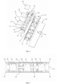
FIG 1 is a structural schematic diagram of an antenna element according to some embodiments of the present application; -
FIG 2 is a schematic exploded view of the antenna element shown inFIG 1 ; -
FIG 3 is a schematic top view of the antenna element shown inFIG 1 ; -
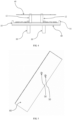
FIG 4 is a schematic side view of the antenna element shown inFIG 1 ; -
FIG 5 is a structural schematic diagram of the antenna element inFIG 1 at another viewing angle; -
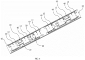
FIG 6 is a structural schematic diagram of an antenna array according to some embodiments of the present application; -
FIG 7 is a schematic exploded view of the antenna array shown inFIG 6 ; and -
FIG 8 is a structural schematic diagram of the antenna array shown inFIG 6 at another viewing angle. - In order to make the objects, technical solutions and advantages of the embodiments of the present application clearer, various embodiments of the present application will be described in detail below with reference to the accompanying drawings. However, those of ordinary skill in the art can appreciate that in the various embodiments of the present application, numerous technical details are set forth in order to provide the reader with a better understanding of the present application. However, the technical solution claimed in the present application can be implemented without these technical details and with various variations and modifications based on the following embodiments. The following division of various embodiments is for convenience of description and should not be construed as limiting the specific implementations of the present application, and various embodiments can be referred to in conjunction with each other without contradiction.
-
FIG. 1 shows a structure of an antenna element according to some embodiments of the present application, andFIG 2 is a schematic exploded view of the antenna element shown inFIG 1 . As shown inFIGS. 1 and2 , an antenna element provided by some embodiments of the present application includes adielectric substrate 10, aradiation unit 20 and afeed unit 30, wherein afirst support column 11 is arranged on thedielectric substrate 10, theradiation unit 20 and thefeed unit 30 are of an integrally formed structure, at least one of theradiation unit 20 and thefeed unit 30 is provided with a first throughhole 21, thefirst support column 11 on thedielectric substrate 10 passes through the first throughhole 21, and thefirst support column 11 on thedielectric substrate 10 and an inner wall of the first throughhole 21 are fixedly connected by means of hot melting. - According to the antenna element provided by some embodiments of the present application, the
radiation unit 20 and thefeed unit 30 are of the integrally formed structure, at least one of theradiation unit 20 and thefeed unit 30 is provided with the first throughhole 21, thefirst support column 11 on thedielectric substrate 10 passes through the first throughhole 21, and is fixedly connected with the inner wall of the first throughhole 21 by means of hot melting, so as to realise assembly among theradiation unit 20 and thefeed unit 30 and thedielectric substrate 10, so that the integrally formedradiation unit 20 andfeed unit 30 and thedielectric substrate 10 can be assembled only by hot melting, and the assembly difficulty of the antenna element is reduced. At the same time, theradiation unit 20 and thefeed unit 30 are of the integrally formed structure so as to avoid the feed network lines and radiation plates of the antenna element from being rough due to adoption of laser engraving or electrochemical plating, thereby reducing the loss of the antenna, and advantageously optimising the gain performance of the antenna. - The
dielectric substrate 10 is a fixing foundation for theradiation unit 20 and thefeed unit 30, theradiation unit 20 is a signal radiation part of the antenna, and thefeed unit 30 plays the role in feeding theradiation unit 20. Compared with the form that the components are independently manufactured and are assembled by connectors in turn, theradiation unit 20 and thefeed unit 30 are of the integrally formed structure and are fixed to the surface of thedielectric substrate 10 by hot melting fit between thefirst support column 11 and the first throughhole 21. In this way, the structural complexity and assembly difficulty caused by the sequential assembly of all components are eliminated. Here, integrally forming of theradiation unit 20 and thefeed unit 30 can be achieved by stamping a metal coil, a metal material is stamped in a preset form to obtain the integrally formedradiation unit 20 andfeed unit 30, and the first throughhole 21 can be stamped in the part where theradiation unit 20 is located or the part where thefeed unit 30 is located, or the parts where theradiation unit 20 and thefeed unit 30 are located. Here, theradiation unit 20 and thefeed unit 30 can also be obtained by digitally controlled lathing, and it is also possible to obtain the integratedradiation unit 20 andfeed unit 30 having a smoother surface compared with laser engraving or electrochemical plating, so as to reduce the loss of the antenna. In addition, thefirst support column 11 on thedielectric substrate 10 can be shaped like a mushroom head after hot melting, and the hole wall of the first throughhole 21 of theradiation unit 20 is fixed to thefirst support column 11, so that theradiation unit 20 andfeed unit 30 of the integrally formed structure are fixed to the surface of thedielectric substrate 10. - In some embodiments, the
radiation unit 20 can take the form of a patch, i.e., the rectangular patch as shown inFIG 2 , while in other embodiments theradiation unit 20 can also take the form of a circular patch or a diamond-shaped patch. In addition, theradiation unit 20 can also take the form of a microstrip line. The feed form of theradiation unit 20 can be coupled feed or direct feed, and thefeed unit 30 is a feed metal strip as shown inFIG 2 . The feed metal strip and the rectangular patch are formed into an integrated structure by stamping metal coils, which can ensure the connection strength between the rectangular patch and the feed metal strip while ensuring the surface accuracy of the rectangular patch and the feed metal strip. - Since the
radiation unit 20 and thefeed unit 30 are fixed on the surface of thedielectric substrate 10, and thefirst support column 11 plays a role in preventing theradiation unit 20 and thefeed unit 30 from being detached from thedielectric substrate 10 after hot melting, the number of thefirst support columns 11 on thedielectric substrate 10 and the number of the first throughholes 21 in the integrally formedradiation unit 20 andfeed unit 30 are not limited, and the number of theradiation units 20 can be designed as one, two, three or five according to actual needs. For example, the number of theradiation units 20 shown inFIG 2 is three, the number of the feed metal strips integrally formed with the threeradiation units 20 is two, the first throughhole 21 is formed in the feed metal strip, the number of second throughholes 41 in each feed metal strip is 11, and the number of thefirst support columns 11 on thedielectric substrate 10 is 22. - In some embodiments, the
dielectric substrate 10 and thefirst support column 11 are made of plastic, and thefirst support column 11 and thedielectric substrate 10 are of an integrally formed structure, so that on the one hand, the weight of the antenna element can be reduced to achieve the light weight of the antenna element, and on the other hand, the connection strength between thefirst support column 11 and thedielectric substrate 10 can be increased to ensure the reliability when theradiation unit 20 and thefeed unit 30 are fixed to thedielectric substrate 10. In other embodiments, thedielectric substrate 10 and thefirst support column 11 can be made of different materials. - In addition to the
radiation unit 20, aparasitic unit 40 is also usually fixed to thedielectric substrate 10 to improve the bandwidth and gain performance of the antenna. Theparasitic unit 40 is spaced apart from theradiation unit 20 to reflect the energy of theradiation unit 20, so that the signals of theradiation unit 20 are superimposed in a specific direction to be enhanced, and the specific direction is the direction in which theradiation unit 20 faces theparasitic unit 40. The fixing between theparasitic unit 40 and thedielectric substrate 10 can also take the form of hot melting of the support column. As shown inFIG 2 , theparasitic unit 40 can be provided with second throughholes 41, and thedielectric substrate 10 can be provided withsecond support columns 12 such that thesecond support columns 12 pass through the second throughhole 41 and are fixedly connected with the hole walls of the second throughholes 41 by hot melting. In such a way, after theradiation unit 20 and thefeed unit 30 are fixed to thedielectric substrate 10, theparasitic unit 40 can be fixed to thedielectric substrate 10 in the same manner. The diameter of the end away from thedielectric substrate 10 of thesecond support column 12 on the dielectric substrate 10is smaller than the diameters of other parts of thesecond support column 12, and the diameter of the second throughhole 41 in theparasitic unit 40 is larger than the diameter of the end away from thedielectric substrate 10 of thesecond support column 12 and smaller than the diameters of other parts of thesecond support column 12. When thesecond support column 12 on thedielectric substrate 10 passes through the second throughhole 41, theparasitic unit 40 will be blocked at the end of thesecond support column 12 and cannot continue to be close to the surface of thedielectric substrate 10. Thus, after the end of thesecond support column 12 is subjected to hot melting to form the mushroom head shape, theparasitic unit 40 is fixed to thesecond support column 12, and theparasitic unit 40 is fixed to the end away from the dielectric substrate 10of thesecond support column 12, and is spaced apart from theradiation unit 20 fixed to the surface of thedielectric substrate 10. - Similarly, the number of the
second support columns 12 on thedielectric substrate 10 and the number of the second throughholes 41 in theparasitic unit 40 are not limited. As shown inFIG 2 , the number of thesecond support columns 12 on thedielectric substrate 10 corresponding to the same oneparasitic unit 40 can be four, and the foursecond support columns 12 are rectangularly arranged on the surface of thedielectric substrate 10 and avoid the mounting position of theradiation unit 20. The number of the second throughholes 41 in theparasitic unit 40 is likewise four, the four second throughholes 41 are likewise rectangularly arranged on theparasitic unit 40, and theparasitic unit 40 can be effectively fixed to thedielectric substrate 10 by the matching between the foursecond support columns 12 on thedielectric substrate 10 and the four second throughholes 41 in theparasitic unit 40. - Meanwhile, the
parasitic units 40 are in one-to-one correspondence to theradiation units 20, oneparasitic unit 40 faces oneradiation unit 20, theparasitic unit 40 can take the form of a metal patch, such as the rectangular metal patch shown inFIG 2 , while in other possible embodiments, theparasitic unit 40 can also take the form of a circular metal patch or a diamond-shaped metal patch. - In addition, in order to improve the bandwidth of the antenna, rectangular matching branches can be loaded on the periphery of the metal patch used as the
parasitic unit 40. Such a rectangular matching branch is a protruding part arranged on the periphery of the metal patch, that is, as shown inFIG 3 , aprotruding portion 42 can be arranged on theparasitic unit 40, and theprotruding portion 42 extends outwards from the edge of theparasitic unit 40. Meanwhile, the protrudingportion 42 can also take other forms, such as a cross shape or a ♀ shape. - In order to improve the gain performance of the antenna, as shown in
FIG. 2 , a plurality of hollowed-outregions 13 can be arranged on thedielectric substrate 10 at positions facing thefeed units 30, each hollowed-outregion 13 faces part of the surface of thefeed unit 30, and the hollowed-outregion 13 is a hollowed-out area formed in thedielectric substrate 10. By hollowing out the position facing thefeed unit 30 on thedielectric substrate 10, the loss of the feed line can be reduced, thereby increasing the gain performance of the antenna. In addition, a certain debugging and optimisation effect is achieved on the phase and standing wave of the antenna. - The hollowed-out region is arranged according to the position of the
feed unit 30, and there may be multiple positions facing the dielectric substrate 10of thefeed unit 30 according to the number of thefeed units 30. As shown inFIG. 2 , the number of thefeed units 30 is two, and the ±45° dual polarisation of theradiation unit 20 can be achieved by the twofeed units 30, so that there are twofeed units 30 integrally formed with theradiation unit 20, and the twofeed units 30 are symmetric about theradiation unit 20. - In addition, the
feed unit 30 can communicate with the outside through afeed pin 50, and the feed pins 50 are in one-to-one correspondence to thefeed units 30, penetrate through thedielectric substrate 10 and are electrically connected with thecorresponding feed units 30. As shown inFIGS. 4 and 5 , one end of thefeed pin 50 is connected to an input end of thefeed unit 30, and the other end of thefeed pin 50 as the input end of the antenna element protrudes out of the surface away from theradiation unit 20 of thedielectric substrate 10 facing and penetrates through theground 60 so that thefeed pin 50 can be electrically connected to a calibration network of the antenna or a filter. Here, the input end of thefeed unit 30 is the end electrically connected with thefeed pin 50. - In some embodiments, the
feed pin 50 can be a metal probe embedded in thedielectric substrate 10, when thedielectric substrate 10 is formed, the metal probe is embedded at a position corresponding to the input end of thefeed unit 30, and after the integrally formedfeed unit 30 andradiation unit 20 are fixed to the surface of thedielectric substrate 10 by means of hot melting, the metal probe is naturally electrically connected with thefeed unit 30, thereby realising signal input. - In addition, the
feed pin 50 is not limited to the form of a metal probe, and can also take the form of a radio frequency connector or the like. Thefeed pin 50 can be connected to an external signal source by means of welding or plugging. - Meanwhile, in order to improve the gain performance of the antenna, the surface current path of the
radiation unit 20 can be increased, theradiation unit 20 has a first edge and a second edge that are opposite to each other, and theradiation unit 20 is provided with anotch 22 recessed from afirst edge 23 to asecond edge 24. Thefirst edge 23 and thesecond edge 24 are the edges of the two opposite sides of the rectangular patch used asradiation unit 20 inFIG. 2 , and thenotch 22 can bend the surface current path of theradiation unit 20. In addition, the surface current path of theradiation unit 20 can also be increased by forming through holes in theradiation unit 20, and the gain performance of the antenna can also be improved. - In order to improve the radiation performance of the antenna, a
flange 14 may be arranged on thedielectric substrate 10, and theflange 14 bends and extends from the edge of thedielectric substrate 10 to the side provided with theradiation unit 20. As shown inFIG. 4 , two long sides of the rectangulardielectric substrate 10 are each provided with theflange 14, and theflange 14 can play a role in reflecting the signal of theradiation unit 20, thereby improving the radiation performance of the antenna. - Some embodiments of the present application also provide an antenna array, as shown in
FIGS. 6-8 , including aground 60 and a plurality of antenna elements in the above-described embodiments, wherein the plurality of antenna elements are arranged in an array on theground 60, and thedielectric substrates 10 of the plurality of antenna elements are of an integrated structure. The antenna element shown inFIG. 6 includes threeradiation units 20, and the antenna array shown inFIG. 6 shows a case where the antenna array includes two antenna elements, which is just one of the schematic structures of the antenna array here. In other possible embodiments, the antenna array can also include three or more antenna elements, and the number of thefeed units 30 and the number of the feed pins 50 can each be four or more correspondingly. - When the antenna array is assembled, it is only necessary to arrange a preset number of antenna elements according to certain rules, such as the linear arrangement shown in
FIG. 6 , and it is not necessary to weld a feed network to the antenna array any longer. In this way, the production operation can be effectively simplified, the number of parts can be greatly reduced, the assembly and welding process of the whole antenna can be simplified, the assembly efficiency can be improved, and automated mass production can be facilitated. - The
ground 60 serves as a metal ground layer arranged on the surface away from theradiation unit 20 of thedielectric substrate 10, in such a way, theground 60 arranged on thedielectric substrate 10 serves as a reflector of the antenna array and the grounding end of theradiation unit 20, and there is no need to add a separate reflector, so that the cost can be reduced, and the weight of the antenna array can be reduced. Here, theground 60 can reflect the electromagnetic wave signal for many times, thereby enhancing the signal receiving and transmitting efficiency of theradiation unit 20. - In addition, as shown in
FIGS. 7 and8 , theground 60 is provided with a third throughhole 61 through which thefeed pin 50 passes, and thefeed pin 50 can pass through the third throughhole 61 in theground 60 to avoid the grounded short circuit of an input port of thefeed pin 50. - It will be understood by those of ordinary skill in the art that the above-described embodiments are specific embodiments for carrying out the present application, and in practice, various changes in form and detail can be made therein without departing from the scope of the present application.
Claims (10)
- An antenna element, comprising a dielectric substrate (10), a radiation unit (20) and a feed unit (30), the dielectric substrate (10) being provided with a first support column (11), the radiation unit (20) and the feed unit (30) being of an integrally formed structure, at least one of the radiation unit (20) and the feed unit (30) being provided with a first through hole (21), the first support column (11) passing through the first through hole (21), and the first support column (11) and an inner wall of the first through hole (21) being fixedly connected by means of hot melting.
- The antenna element according to claim 1, wherein:
the dielectric substrate (10) and the first support column (11) are made of plastic, and the first support column (11) and the dielectric substrate (10) are of an integrally formed structure. - The antenna element according to claim 1, wherein:
further comprising a parasitic unit (40), the parasitic unit (40) being provided with a second through hole (41), the dielectric substrate (10) being provided with a second support column (12), the second support column (12) passing through the second through hole (21), and the second support column (12) and an inner wall of the second through hole (21) being fixedly connected by means of hot melting, and the parasitic unit (40) being spaced apart from the radiation unit (20). - The antenna element according to claim 3, wherein:
the parasitic unit (40) is provided with a protruding portion (42), and the protruding portion (42) extends outwards from an edge of the parasitic unit (40). - The antenna element according to any one of claims 1 to 4, wherein:
the dielectric substrate (10) is provided with a plurality of hollowed-out regions (13), and the hollowed-out regions (13) are arranged facing a surface of the feed unit (30). - The antenna element according to claim 1, wherein:
a number of the feed units (30) is two, and the two feed units (30) are symmetric relative to the radiation unit (20). - The antenna element according to claim 1 or 6, wherein:
further comprising feed pins (50), the feed pins (50) being in one-to-one correspondence to the feed units (30), and the feed pins (50) penetrating through the dielectric substrate (10) and being electrically connected with the corresponding feed units (30). - The antenna element according to claim 1, wherein:
the radiation unit (20) has a first edge (23) and a second edge (24) that are arranged opposite to each other, and the radiation unit (20) is provided with a notch (22) which is recessed from the first edge (23) to the second edge (24). - The antenna element according to claim 1, wherein:
the dielectric substrate (10) is provided with a flange (14), and the flange (14) bends and extends from an edge of the dielectric substrate (10) to a side provided with the radiation unit (20). - An antenna array, comprising:
a ground (60) and a plurality of antenna elements according to any one of claims 1 to 9, the plurality of antenna elements being arranged in an array on the ground (60), and the dielectric substrates (10) of the plurality of antenna elements being of an integrated structure.
Applications Claiming Priority (2)
| Application Number | Priority Date | Filing Date | Title |
|---|---|---|---|
| CN202111040176.6A CN115775972A (en) | 2021-09-06 | 2021-09-06 | Antenna element and antenna array |
| PCT/CN2022/115985 WO2023030342A1 (en) | 2021-09-06 | 2022-08-30 | Antenna element and antenna array |
Publications (2)
| Publication Number | Publication Date |
|---|---|
| EP4391225A1 true EP4391225A1 (en) | 2024-06-26 |
| EP4391225A4 EP4391225A4 (en) | 2024-12-11 |
Family
ID=85387511
Family Applications (1)
| Application Number | Title | Priority Date | Filing Date |
|---|---|---|---|
| EP22863477.0A Pending EP4391225A4 (en) | 2021-09-06 | 2022-08-30 | ANTENNA ELEMENT AND GROUP ANTENNA |
Country Status (4)
| Country | Link |
|---|---|
| US (1) | US12603431B2 (en) |
| EP (1) | EP4391225A4 (en) |
| CN (1) | CN115775972A (en) |
| WO (1) | WO2023030342A1 (en) |
Families Citing this family (2)
| Publication number | Priority date | Publication date | Assignee | Title |
|---|---|---|---|---|
| US12176614B2 (en) * | 2022-10-28 | 2024-12-24 | Wuhan Fingu Electronic Technology Co., Ltd. | Antenna |
| CN119234353B (en) | 2023-04-28 | 2026-01-16 | 京东方科技集团股份有限公司 | Antenna and electronic equipment |
Family Cites Families (12)
| Publication number | Priority date | Publication date | Assignee | Title |
|---|---|---|---|---|
| JP2007221513A (en) | 2006-02-17 | 2007-08-30 | Chant Sincere Co Ltd | Casing of wireless communication product with common antenna |
| KR100910161B1 (en) * | 2009-02-25 | 2009-07-30 | 주식회사 에이티앤씨 | Built-in antenna integrated portable terminal case and manufacturing method thereof |
| CN105958195A (en) * | 2016-06-12 | 2016-09-21 | 苏州市吴通天线有限公司 | Dual-channel dual-frequency built-in antenna apparatus |
| CN207009632U (en) * | 2017-06-18 | 2018-02-13 | 上海深迅通信技术有限公司 | A CDMA bracket antenna for vehicle-mounted OBD |
| CN108987947B (en) | 2018-06-27 | 2024-04-16 | 广东通宇通讯股份有限公司 | 3D-MID technology array antenna |
| CN111063996A (en) * | 2019-12-31 | 2020-04-24 | 华南理工大学 | Antenna module and 5G antenna |
| CN111490317B (en) | 2020-05-14 | 2025-01-24 | 京信通信技术(广州)有限公司 | Dielectric sliding phase shifter and base station antenna |
| CN212303916U (en) | 2020-06-28 | 2021-01-05 | 江苏嘉华通讯科技有限公司 | Low-frequency-band small base station antenna |
| EP4197059B1 (en) * | 2020-08-13 | 2025-12-31 | Telefonaktiebolaget LM Ericsson (publ) | Antenna beamer and antenna |
| CN112787081A (en) * | 2020-12-31 | 2021-05-11 | 深圳慧联达科技有限公司 | Massive MIMO array antenna and base station |
| CN112864600B (en) | 2021-01-22 | 2025-04-29 | 苏州硕贝德创新技术研究有限公司 | High cross-polarization ratio patch antenna and communication base station |
| CN113140898A (en) * | 2021-04-06 | 2021-07-20 | 深圳市信维通信股份有限公司 | Oscillator antenna |
-
2021
- 2021-09-06 CN CN202111040176.6A patent/CN115775972A/en active Pending
-
2022
- 2022-08-30 EP EP22863477.0A patent/EP4391225A4/en active Pending
- 2022-08-30 WO PCT/CN2022/115985 patent/WO2023030342A1/en not_active Ceased
- 2022-08-30 US US18/687,815 patent/US12603431B2/en active Active
Also Published As
| Publication number | Publication date |
|---|---|
| US20250125527A1 (en) | 2025-04-17 |
| CN115775972A (en) | 2023-03-10 |
| EP4391225A4 (en) | 2024-12-11 |
| US12603431B2 (en) | 2026-04-14 |
| WO2023030342A1 (en) | 2023-03-09 |
Similar Documents
| Publication | Publication Date | Title |
|---|---|---|
| CN110676577B (en) | Antenna element and array antenna | |
| KR102092813B1 (en) | Stacked patch antenna elements and antenna assemblies | |
| US9270027B2 (en) | Notch-antenna array and method for making same | |
| US11050163B2 (en) | Array antenna | |
| US9112270B2 (en) | Planar array feed for satellite communications | |
| US12500352B2 (en) | Low-profile, wideband electronically scanned array for integrated geo-location, communications, and radar | |
| KR20230048359A (en) | antenna array | |
| EP4391225A1 (en) | Antenna element and antenna array | |
| CN113517550B (en) | 5G dual polarized antenna radiating element and base station antenna | |
| US20150002356A1 (en) | Tube and ring directional end-fire array antenna | |
| CN210468111U (en) | Antenna oscillator and array antenna | |
| US12394900B2 (en) | Bandwidth extended balanced tightly coupled dipole array additively manufactured modular aperture | |
| US20230081591A1 (en) | Notch antenna array | |
| CN212485546U (en) | Radiating element, antenna assembly and base station antenna | |
| CN117199769A (en) | Spliced dual-polarized dovetail groove metal Vivaldi antenna | |
| WO2022139985A1 (en) | Antenna connector and antenna | |
| US12555923B2 (en) | Transparent oscillator unit, transparent antenna and antenna system | |
| CN217182414U (en) | Miniaturized high-gain narrow-beam antenna | |
| CN214625493U (en) | Antenna connector and antenna | |
| EP4205237B1 (en) | A notch antenna structure | |
| Reljic et al. | Analysis of combining separate complex planar PCB antenna arrays into bigger antenna systems for high gain and demanding radar applications | |
| JP4333328B2 (en) | Slot antenna with sealed reflector | |
| CN121399795A (en) | Radiating element for antenna | |
| CN117748163A (en) | Feed network component and array antenna | |
| CN121097393A (en) | Small-sized base station antenna |
Legal Events
| Date | Code | Title | Description |
|---|---|---|---|
| STAA | Information on the status of an ep patent application or granted ep patent |
Free format text: STATUS: THE INTERNATIONAL PUBLICATION HAS BEEN MADE |
|
| PUAI | Public reference made under article 153(3) epc to a published international application that has entered the european phase |
Free format text: ORIGINAL CODE: 0009012 |
|
| STAA | Information on the status of an ep patent application or granted ep patent |
Free format text: STATUS: REQUEST FOR EXAMINATION WAS MADE |
|
| 17P | Request for examination filed |
Effective date: 20240321 |
|
| AK | Designated contracting states |
Kind code of ref document: A1 Designated state(s): AL AT BE BG CH CY CZ DE DK EE ES FI FR GB GR HR HU IE IS IT LI LT LU LV MC MK MT NL NO PL PT RO RS SE SI SK SM TR |
|
| REG | Reference to a national code |
Ref country code: DE Ref legal event code: R079 Free format text: PREVIOUS MAIN CLASS: H01Q0001360000 Ipc: H01Q0001120000 |
|
| A4 | Supplementary search report drawn up and despatched |
Effective date: 20241112 |
|
| DAV | Request for validation of the european patent (deleted) | ||
| DAX | Request for extension of the european patent (deleted) | ||
| RIC1 | Information provided on ipc code assigned before grant |
Ipc: H01Q 21/00 20060101ALN20241106BHEP Ipc: H01Q 1/24 20060101ALN20241106BHEP Ipc: H01Q 21/08 20060101ALN20241106BHEP Ipc: H01Q 9/04 20060101ALI20241106BHEP Ipc: H01Q 1/12 20060101AFI20241106BHEP |
|
| STAA | Information on the status of an ep patent application or granted ep patent |
Free format text: STATUS: EXAMINATION IS IN PROGRESS |