EP4391224A1 - Integrated vehicle antenna absorber - Google Patents
Integrated vehicle antenna absorber Download PDFInfo
- Publication number
- EP4391224A1 EP4391224A1 EP22215894.1A EP22215894A EP4391224A1 EP 4391224 A1 EP4391224 A1 EP 4391224A1 EP 22215894 A EP22215894 A EP 22215894A EP 4391224 A1 EP4391224 A1 EP 4391224A1
- Authority
- EP
- European Patent Office
- Prior art keywords
- antenna
- waveguide
- sensor assembly
- slots
- vehicle sensor
- Prior art date
- Legal status (The legal status is an assumption and is not a legal conclusion. Google has not performed a legal analysis and makes no representation as to the accuracy of the status listed.)
- Pending
Links
- 239000006096 absorbing agent Substances 0.000 title description 20
- 238000000576 coating method Methods 0.000 claims abstract description 42
- 239000000463 material Substances 0.000 claims abstract description 42
- 239000011248 coating agent Substances 0.000 claims abstract description 38
- 230000005670 electromagnetic radiation Effects 0.000 claims abstract description 8
- 239000012799 electrically-conductive coating Substances 0.000 claims description 27
- 238000003491 array Methods 0.000 claims description 22
- 238000005266 casting Methods 0.000 claims description 10
- 239000010410 layer Substances 0.000 description 24
- 239000004020 conductor Substances 0.000 description 15
- 230000008901 benefit Effects 0.000 description 9
- 238000000034 method Methods 0.000 description 7
- 230000000712 assembly Effects 0.000 description 6
- 238000000429 assembly Methods 0.000 description 6
- 229910052751 metal Inorganic materials 0.000 description 6
- 239000002184 metal Substances 0.000 description 5
- 230000010355 oscillation Effects 0.000 description 4
- 230000008569 process Effects 0.000 description 4
- VYZAMTAEIAYCRO-UHFFFAOYSA-N Chromium Chemical compound [Cr] VYZAMTAEIAYCRO-UHFFFAOYSA-N 0.000 description 3
- 229910052804 chromium Inorganic materials 0.000 description 3
- 239000011651 chromium Substances 0.000 description 3
- 238000009713 electroplating Methods 0.000 description 3
- 210000003195 fascia Anatomy 0.000 description 3
- 238000012986 modification Methods 0.000 description 3
- 230000004048 modification Effects 0.000 description 3
- 238000000206 photolithography Methods 0.000 description 3
- 238000007747 plating Methods 0.000 description 3
- HCHKCACWOHOZIP-UHFFFAOYSA-N Zinc Chemical compound [Zn] HCHKCACWOHOZIP-UHFFFAOYSA-N 0.000 description 2
- 238000010521 absorption reaction Methods 0.000 description 2
- 238000004891 communication Methods 0.000 description 2
- 239000011521 glass Substances 0.000 description 2
- 238000003384 imaging method Methods 0.000 description 2
- 239000007769 metal material Substances 0.000 description 2
- 238000005240 physical vapour deposition Methods 0.000 description 2
- 238000004544 sputter deposition Methods 0.000 description 2
- 239000011701 zinc Substances 0.000 description 2
- 229910052725 zinc Inorganic materials 0.000 description 2
- RYGMFSIKBFXOCR-UHFFFAOYSA-N Copper Chemical compound [Cu] RYGMFSIKBFXOCR-UHFFFAOYSA-N 0.000 description 1
- BQCADISMDOOEFD-UHFFFAOYSA-N Silver Chemical compound [Ag] BQCADISMDOOEFD-UHFFFAOYSA-N 0.000 description 1
- 239000012790 adhesive layer Substances 0.000 description 1
- 239000004411 aluminium Substances 0.000 description 1
- 229910052782 aluminium Inorganic materials 0.000 description 1
- XAGFODPZIPBFFR-UHFFFAOYSA-N aluminium Chemical compound [Al] XAGFODPZIPBFFR-UHFFFAOYSA-N 0.000 description 1
- 238000013459 approach Methods 0.000 description 1
- 230000005540 biological transmission Effects 0.000 description 1
- 230000015556 catabolic process Effects 0.000 description 1
- 238000003486 chemical etching Methods 0.000 description 1
- 238000004140 cleaning Methods 0.000 description 1
- 229910052802 copper Inorganic materials 0.000 description 1
- 239000010949 copper Substances 0.000 description 1
- 230000008878 coupling Effects 0.000 description 1
- 238000010168 coupling process Methods 0.000 description 1
- 238000005859 coupling reaction Methods 0.000 description 1
- 238000006731 degradation reaction Methods 0.000 description 1
- 238000013461 design Methods 0.000 description 1
- 238000001514 detection method Methods 0.000 description 1
- 238000002059 diagnostic imaging Methods 0.000 description 1
- 230000009977 dual effect Effects 0.000 description 1
- 238000005516 engineering process Methods 0.000 description 1
- 238000005530 etching Methods 0.000 description 1
- 230000008020 evaporation Effects 0.000 description 1
- 238000001704 evaporation Methods 0.000 description 1
- 230000003116 impacting effect Effects 0.000 description 1
- 238000004519 manufacturing process Methods 0.000 description 1
- 238000001465 metallisation Methods 0.000 description 1
- 238000005459 micromachining Methods 0.000 description 1
- 238000012544 monitoring process Methods 0.000 description 1
- 229910001120 nichrome Inorganic materials 0.000 description 1
- 238000000059 patterning Methods 0.000 description 1
- 230000035699 permeability Effects 0.000 description 1
- 229920002120 photoresistant polymer Polymers 0.000 description 1
- 239000004332 silver Substances 0.000 description 1
- 229910052709 silver Inorganic materials 0.000 description 1
- 239000004557 technical material Substances 0.000 description 1
- 238000012360 testing method Methods 0.000 description 1
- 230000007704 transition Effects 0.000 description 1
Images



Classifications
-
- H—ELECTRICITY
- H01—ELECTRIC ELEMENTS
- H01Q—ANTENNAS, i.e. RADIO AERIALS
- H01Q1/00—Details of, or arrangements associated with, antennas
- H01Q1/27—Adaptation for use in or on movable bodies
- H01Q1/32—Adaptation for use in or on road or rail vehicles
- H01Q1/3208—Adaptation for use in or on road or rail vehicles characterised by the application wherein the antenna is used
- H01Q1/3233—Adaptation for use in or on road or rail vehicles characterised by the application wherein the antenna is used particular used as part of a sensor or in a security system, e.g. for automotive radar, navigation systems
-
- H—ELECTRICITY
- H01—ELECTRIC ELEMENTS
- H01Q—ANTENNAS, i.e. RADIO AERIALS
- H01Q1/00—Details of, or arrangements associated with, antennas
- H01Q1/52—Means for reducing coupling between antennas; Means for reducing coupling between an antenna and another structure
- H01Q1/521—Means for reducing coupling between antennas; Means for reducing coupling between an antenna and another structure reducing the coupling between adjacent antennas
- H01Q1/523—Means for reducing coupling between antennas; Means for reducing coupling between an antenna and another structure reducing the coupling between adjacent antennas between antennas of an array
-
- H—ELECTRICITY
- H01—ELECTRIC ELEMENTS
- H01Q—ANTENNAS, i.e. RADIO AERIALS
- H01Q21/00—Antenna arrays or systems
- H01Q21/0006—Particular feeding systems
- H01Q21/0037—Particular feeding systems linear waveguide fed arrays
- H01Q21/0043—Slotted waveguides
- H01Q21/005—Slotted waveguides arrays
-
- G—PHYSICS
- G01—MEASURING; TESTING
- G01S—RADIO DIRECTION-FINDING; RADIO NAVIGATION; DETERMINING DISTANCE OR VELOCITY BY USE OF RADIO WAVES; LOCATING OR PRESENCE-DETECTING BY USE OF THE REFLECTION OR RERADIATION OF RADIO WAVES; ANALOGOUS ARRANGEMENTS USING OTHER WAVES
- G01S13/00—Systems using the reflection or reradiation of radio waves, e.g. radar systems; Analogous systems using reflection or reradiation of waves whose nature or wavelength is irrelevant or unspecified
- G01S13/88—Radar or analogous systems specially adapted for specific applications
- G01S13/93—Radar or analogous systems specially adapted for specific applications for anti-collision purposes
- G01S13/931—Radar or analogous systems specially adapted for specific applications for anti-collision purposes of land vehicles
Definitions
- sensor assemblies such as RADAR sensor assemblies for vehicles.
- sensor assemblies disclosed herein comprise an antenna portion and/or piece comprising dual properties and/or materials, which may allow for combining the functionality of an electromagnetic absorber with that of an antenna.
- this combination may be achieved by forming certain portions of the sensor/antenna/waveguide assembly from a suitable lossy and/or absorptive material configured to cancel or at least reduce electromagnetic signal reflection interference and applying an electrically conductive coating to certain regions of the assembly, such as to the regions defining antenna slots, regions adjacent to the antenna slots, and/or other regions in which electrical conductivity is needed or desired.
- the antenna slots may be formed in a separate piece and/or layer, such as to an antenna plate configured to be coupled with a separate waveguide piece of the assembly.
- This piece may be made up of, either wholly or partially, a suitable lossy and/or absorptive material configured to reduce electromagnetic interference caused by, for example, fascia reflections. Selected portions of this separate piece may then be electroplated, coated, and/or treated with a suitable metal or other electrically conductive material.
- the walls defining antenna slots in the antenna piece may be treated with such a metal or other conductive material layer, which may be helpful in improving performance in near field regions.
- other regions of the antenna plate/piece may be treated, such as in some cases an entire surface and/or side of the plate that is configured to be coupled with a waveguide piece of the assembly.
- the entire assembly, or at least a larger part of the assembly comprising both antenna and waveguide features may be formed from a unitary, single structure, such as a molded piece, casting, or the like, for example.
- this piece may be molded from the aforementioned absorptive and/or lossy material and then selectively coated and/or treated with the aforementioned conductive material(s) in regions where conductivity may be needed or desired.
- the regions defining the antenna slots may, in such embodiments, may be so treated/coated, in some cases along with adjacent regions.
- Other regions, such as posts or other structures defining the waveguides may also be treated/coated, if desired.
- the assembly may comprise a waveguide part and an antenna part operably coupled with the waveguide part.
- the antenna part may comprise an array of antenna slots, wherein each of the antenna slots is configured to deliver electromagnetic radiation from the waveguide part therethrough.
- the antenna part may be at least partially defined by a lossy and/or absorptive material configured to reduce electromagnetic radiation reflections.
- the antenna part may further comprise an electrically conductive and/or metallic coating, which may be applied to the absorptive material of the antenna part, at least in part, to provide desired properties in these regions.
- the waveguide part may comprise a first layer of the assembly, such as a plate, for example, and the antenna part may comprise a second layer of the assembly, such as a molded piece, coupled to the first layer.
- the electrically conductive and/or metallic coating may be applied to an entire surface, or at least substantially an entire surface, of an inner side of the second layer adjacent to the first layer. In some embodiments, however, the electrically conductive and/or metallic coating may be applied only partially to an outer side of the second layer. In some embodiments, the electrically conductive coating may be applied to a region of the outer side of the second layer adjacent to one or more, or in some cases each, of the antenna slots.
- the waveguide part may comprise an array of waveguide grooves.
- the antenna part and the array of waveguide grooves may both be part of an integrally formed mold and/or casting.
- each waveguide groove of the array of waveguide grooves may be formed by two or more opposing rows of posts formed in the mold/casting.
- the electrically conductive coating may be applied to each of the posts.
- At least a subset of the antenna slots may comprise an array of staggered antenna slot arrays each comprising a first row of antenna slots extending along a first line and a second row of antenna slots extending along a second line and offset from the first row of antenna slots.
- the electrically conductive coating may be applied to walls defining each antenna slot of each staggered antenna slot array. In some cases, this coating may be applied so as to wholly cover each of these walls.
- each of the staggered antenna slot arrays may be positioned in a respective bounded region of the antenna part in which each slot of each staggered antenna slot array is wholly contained.
- the electrically conductive coating may be applied to each of the bounded regions of the antenna part.
- the waveguide part may comprise a metallic block and/or the antenna part may comprise a plate coupled to the metallic block.
- the plate may comprise an electrically conductive coating at least substantially covering the plate on a side facing the metallic block.
- the electrically conductive and/or metallic coating may be applied to each wall defining each of the antenna slots.
- the electrically conductive and/or metallic coating may comprise an electroplated coating.
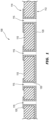
- FIG. 1 depicts a cross-sectional view of a waveguide/sensor assembly 100, or a portion thereof, such as a RADAR sensor assembly for a vehicle.
- a portion 110 of the assembly 100 preferably comprising an absorber or an absorptive material is shown making up the bulk/core of the portion of the assembly 100 depicted in the figure.
- a series of antenna slots 115 extend through portion 110.
- each antenna slots 115 would typically be operably coupled with a waveguide, such as, for example, a waveguide comprising waveguide grooves.
- assembly 100 may comprise only a selected portion of a larger waveguide and/or antenna assembly, such as a plate and/or layer of such a larger assembly with another portion of the larger assembly defining the waveguides.
- assembly 100 may comprise a single, unitary, and/or self-contained assembly that itself defines the waveguides. More specific examples of both of these embodiments will be described in greater detail in connection with other figures below.
- the absorptive material making up portion 110 may comprise a lossy material configured to absorb electromagnetic radiation/signals, such as RADAR signals.
- this lossy material may have a dielectric constant of between about 4 and about 12.
- the dielectric constant may be between about 6 and about 9. In a very specific example of a preferred embodiment, the dielectric constant may be about 8.
- the absorptive material may comprise a lossy material having a dielectric constant of between about 6 and about 14.
- the dielectric constant may be between about 9 and about 14 or between about 6 and about 9.
- the absorptive material of portion 110 may have a dielectric loss tangent of between about 0.1 and about 0.7. More preferably, the dielectric loss tangent of the material may be between about 0.15 and about 0.65. In some such embodiments, the dielectric loss tangent of the material may be between about 0.3 and about 0.6, or more preferably between about 0.5 and about 0.6. In a very specific example of a preferred embodiment, the dielectric loss tangent of the material may be about 0.56.
- the absorptive material may have a dielectric loss tangent of between about 0.2 and about 0.6.
- the dielectric loss tangent of the material may be between about 0.3 and about 0.6, or between about 0.2 and about 0.3.
- one or both of these parameters may vary within about +/- 20%.
- the lossy and/or absorptive material of assembly 100 has an electrically conductive coating 120, such as a metallic coating in preferred embodiments.
- metallic coating 120 extends along each of the walls defining each of the various antenna slots 115.
- the entire side/surface of portion 110 on a first side 112 of assembly 100 comprises metallic coating 120.
- a second side 114 of assembly 100 opposite from first side 112 only partially comprises metallic coating 120, with the coating 120 extending along side 114 only in the regions adjacent to the antenna slot 115 openings.
- the conductive and/or metallic coating 120 may comprise, for example, Copper, Nichrome, Aluminium, Silver, or Zinc. As those of ordinary skill in the art will appreciate, different coating materials may be more suitable for specific processes, applications, and/or functions.
- the coating 120/220 is applied only partially between adjacent slots 115/215A/215B, in alternative embodiments, this coating may instead be applied continuously from slot to slot. Similarly, in other embodiments, the coating may be applied only along the slot walls and need not be applied between the slots along the adjacent surface(s) at all, allowing absorptive material to wholly extend between and around the slots along the adjacent surfaces, such as the upper and/or lower surface.
- the coating extends beyond the region defining the slots
- the coating extends symmetrically in this adjacent region, such as in the adjacent surface (surface 114 in FIG. 1 and the surface depicted in FIG. 2 , for example).
- the coating may at least extend symmetrically along the azimuth plane in this area.
- the coating 220 extends symmetrically along the long sides of the slots 215A and/or 215B, as shown in FIG. 2 , due to the higher influence on the antenna near fields in these regions.
- the coating 120 is selectively applied only in regions where required or reasonably necessary, such as parts/portions requiring electrical conductivity.
- this surface may contact an adjacent waveguide portion of the assembly.
- the antenna function and the absorber function which are typically provided by two separate pieces of a RADAR/sensor assembly, may be combined or integrated into one piece.
- conductive and/or metallic coating 120 may comprise an electroplated coating.
- coating 120 may be applied in other ways, such as using, for example, metal patterning, metal deposition, and/or photolithography.
- conductive and/or metallic coatings may be applied using, for example, physical vapor deposition (PVD) processes, which may include sputter deposition (sputtering) and evaporation.
- PVD physical vapor deposition
- the coating process may include the use of plasma cleaning in order to give a clean surface for the coating to be applied on.
- a thin adhesive layer of chromium may be sputtered in order to improve the adhesion between absorber material and the conductive and/or metallic coating.
- selective plating may be applied by creating a pattern on a mask.
- This process may involve chemical etching, micromachining, and/or photolithography.
- a mask for this purpose may be, for example, a glass plate patterned with chromium on one side.
- photolithography by projecting UV light onto the mask, the pattern may be printed to the photoresist, since glass is transparent under UV light while chromium is opaque.
- Another potentially suitable approach may involve plating the structure and then creating a negative pattern on the mask, which may then be subject to an etching process again.
- absorption properties such as absorption for reflection cancellation due to, for example, fascia reflections
- absorption properties may be achieved without unduly impacting antenna performance, which often happens when an absorptive material is used in regions close to the antennae near field(s).
- the principles disclosed herein may allow for engineering electromagnetic properties in such a way that cannot be exhibited by conventional materials.
- An absorber with such features and/or characteristics may thereby utilize its effective complex permittivity and permeability to address various issues present in, for example, vehicle antennae/sensors, such as reflection cancellation, while minimizing or at least reducing antenna performance.
- the walls defining antenna slots 115 may only be partially covered with a suitable electroplating or other conductive material 120.
- some antenna slots 115 in certain configurations may be left without any such conductive layer.
- some embodiments may be configured such that side 112 has certain portions that lack conductive layer 120 such that the absorptive material 110 is exposed. Similarly, some embodiments may comprise no conductive layer 120 along side 114, or may comprise a larger portion of this side 114 with conductive layer 120 depending upon, for example, the spacing of the antenna slots, the desired use of the antenna/sensor, etc.
- FIGS. 2 and 3 depict opposite sides, respectively, of an embodiment of a waveguide/sensor assembly 200, or a portion thereof, according to another embodiment.
- the waveguide/sensor assembly 200 can be regarded as a vehicle sensor assembly.
- FIG. 2 depicts a first side of assembly 200, which includes a first array of antenna slots 215A and a second array of antenna slots 215B.
- array of antenna slots 215A may comprise an RX section and antenna slots 215B may comprise a TX section of the assembly 200.
- respective waveguide grooves 218A/218B may be formed, which may direct electromagnetic radiation to and/or from one or more respective antenna slots 215A/215B.
- the grooves 218A/218B may according to some aspects constitute a waveguide part.
- RX slots 215A comprise elongated, straight slots
- TX slots 215B comprise curved or "wavy" slots that, as shown in FIG. 2 , oscillate back and forth between opposing sides of an elongated axis.
- TX slots 215B further comprise an optional phase-compensating feature. In the depicted embodiment, this is accomplished by applying one or more angled and/or tapered sections, such as tapered grooves or cutouts, along the slots.
- the depicted embodiment illustrates a tapered and/or angled section/surface that is formed along both opposing sidewalls defining each antenna slot 215B at points of maxima for the oscillating pattern of the respective slot.
- These tapering sections may comprise a stepped taper or ledge or may comprise a smoothly transitioning taper.
- a ledge may be formed at the starting point of the taper and therefore, rather than a smooth taper between the outer surface of the structure defining the slot 215B and the starting point of the tapering section, the transition of the tapering section may be immediate from the starting point, which is at a ledge of section to the outer surface of the structure forming the slot.
- all of the peaks/maxima of the oscillating pattern of slots 215B may comprise a phase-compensating feature.
- only a subset of the peaks/maxima defined by slots 215B may comprise such a feature.
- no such phase-compensating feature may be included at all.
- each of at least a subset of the plurality of the tapering surfaces/sections may be spaced apart in a manner that coincides with the intermittent oscillation of the slots 215B.
- all of the tapering surfaces/sections may be spaced apart in a manner that coincides with the intermittent oscillation of the slots 215B.
- stepped taper of assembly 200 is but an example for purposes of illustration and that a wide variety of alternative embodiments are contemplated.
- any number of steps may be used in between the one step shown in this embodiment and an effectively infinite number of steps involved in a smooth taper.
- Each of the tapering sections of assembly 200 may comprise a stepped taper extending between a first edge of the ledge formed by the tapering section, which first edge may be positioned in between the external surface of the structure forming slots 215B and the internal surface of this structure, and a second edge of a concavely curved surface (in some cases, a semi-circular concavely curved surface), the second edge extending along the external surface of the aforementioned structure.
- any number of intermediate steps may be used as desired.
- these sections/surfaces may be positioned so as to alternate and be staggered along the opposing slot sidewalls such that each section is positioned at a particular point along the axis of along only one sidewall of each respective slot 215B.
- each section may be formed along one of the peaks of each oscillating respective slot 215B.
- the antenna slot defines, or at least substantially defines, a sine wave
- each of the tapering/phase-compensating sections is preferably formed along one of the peaks of the sine wave extending towards the axial center of the slot 215B and/or accompanying waveguide.
- all of the aforementioned peaks may comprise a phase-compensating feature.
- only a subset of the peaks defined by each respective slot 215B may comprise such a feature.
- each respective slot 215B may intermittently oscillate on opposite sides of the elongated axis of each respective slot 215B and/or adjacent waveguide along at least a portion thereof.
- each of at least a subset of the plurality of the tapering surfaces/sections may be spaced apart in a manner that coincides with the intermittent oscillation of each respective slot 215B.
- all of the tapering surfaces/sections may be spaced apart in a manner that coincides with the intermittent oscillation of each respective slot 215B.
- each of the plurality of tapering sections surfaces may comprise a first set of tapering surfaces on a first side of each respective slot 215B and a second set of tapering surfaces on a second side of each respective slot 215B opposite the first side.
- the tapering surfaces/sections alternate such that each tapering surface of first set of tapering surfaces is positioned adjacent to one or more tapering surfaces of the second set of tapering surfaces along the axis of each respective slot 215B and each tapering surface of the second set of tapering surfaces is positioned adjacent to one or more tapering surfaces of the first set of tapering surfaces along the axis, again, preferably alternating back and forth across each respective slot 215B.
- Each of the plurality of tapering surfaces/sections may comprise a curved, tapering surface, as shown in FIG. 2 .
- each of the tapering surfaces/sections is defined, at least in part, by a semi-circular cutout, which may be formed at the exterior surface of each respective slot 215B, as a concave region from the convex region of the curve defined by each respective slot 215B, and then may taper down to a corner, edge, or starting point of the taper.
- the tapers of one or more (or each) of the tapering sections do not extend all the way between opposing surfaces of the structure of assembly 200 defining slots 215B, but rather start at a point between the opposing surfaces of this structure and extend to the upper/outer portion of slots 215B on the side opposite the aforementioned waveguides, which are on the opposite side of assembly 200, as shown in FIG. 3 .
- the starting point(s) of the tapering sections may be sufficiently spaced from the (typically inner) surface from which the slot(s) 215B originates.
- the starting point may be located at a point no less than 20%, or no less than about 20%, of the distance from the lower/inner and/or originating surface of the slot(s) to the upper/outer and/or terminating surface of the slot(s).
- the tapering surfaces/sections may instead be straight or non-curved.
- the curvature of the tapering sections may extend in multiple dimensions.
- a semi-spherically curved surface may be formed within one or more of these tapering sections if desired. Additional details regarding these phase-compensating features can be found in U.S. Patent Application Serial No. 17/370,922 titled PHASE-COMPENSATED WAVEGUIDES AND RELATED SENSOR ASSEMBLIES, the entire contents of which are hereby incorporated by reference herein.
- each of the various antenna slots is defined and/or coated, wholly or at least in part, by an electrically conductive plating/coating/layer 220.
- this conductive material 220 also extends adjacent to each of the slots 215A/215B on the adjacent surface, as shown in FIG. 2 .
- the material making up assembly 200 otherwise may comprise an absorptive material 210, which may comprise any of the absorptive materials mentioned herein.
- FIG. 3 depicts assembly 200 from the side opposite to that of FIG. 2 .
- the waveguide structures of the assembly 200 are depicted. More particularly, several rows of posts 222 are depicted. In between two or more rows of posts on each opposing side, a series of waveguides are defined.
- waveguides may be defined in between a single row of posts on each side or waveguides may be defined in other ways, such as trench-style waveguides lacking posts altogether.
- this conductive material layer 220 may also be applied to each of the posts 222, either wholly or in part (such as on each top surface of each post 222). As shown in FIG. 3 , however, some embodiments, including the depicted embodiment, may comprise an electroplating or other conductive layer/coating 220 applied to other regions of the waveguide side of the assembly 200. For example, in the depicted embodiment, all of the posts 222 are conductively coated in their entireties, along with the adjacent waveguide regions. In some embodiments, the entire surface defining the waveguides may be coated with a suitable electrically conductive material. However, as shown in FIG. 3 , in some embodiments, certain regions of the assembly 200 not requiring conductivity and/or that may benefit from exposed absorptive materials need not be coated/layered with material 220.
- FIGS. 4-6 depict another antenna and/or sensor assembly according to still other embodiments.
- a separate plate or other piece is used for the antenna slots of the assembly.
- This separate piece is preferably formed, in some cases wholly formed (aside from the conductive coating(s)/cover(s)/treatment(s) discussed below), from a suitable absorptive material, including any of those discussed elsewhere herein.
- the separate antenna/absorber piece may then be treated in selected regions with a metal or other electrically conductive material, including any of those materials discussed herein.
- this treatment comprises an electroplating of a metal in the regions defining the sidewalls of the antenna slots.
- this treatment comprises further coating of adjacent regions of the antenna/absorber piece, such as regions extending along an upper surface of the piece adjacent to the antenna slots in the case of the piece being a plate.
- the lower side/surface of the assembly may be treated/coated, in some cases so as to encompass the entire lower side/surface, to facilitate desired coupling with the requisite electrical contact with another piece/layer of the assembly.
- the entire lower surface may be treated/coated, or at least substantially entirely treated/coated, with the desired conductive material(s).
- antenna plate 400 generally an antenna part 400, but more particularly an antenna plate 400 in the depicted embodiment, is shown.
- antenna plate 400 defines the antenna slots of the assembly and may be coupled with one or more other elements to complete the assembly, such as a waveguide piece 402, generally a waveguide part 402, shown in FIGS. 5 and 6 .
- the antenna/absorber piece 400 comprises-in some cases wholly comprises aside from the conductive materials described below-an absorptive material 410, which may, for example, reduce signal degradation due to reflection from fascia materials of a vehicle and the like by absorbing such reflected signals.
- the waveguide part 402 comprises a first layer 402 of a vehicle sensor assembly 500 having multiple layers and the antenna part 400 comprises a second and/or upper layer 400 of the assembly 500 coupled to the first layer 402.
- the waveguide part 218A/218B and antenna part 205 may be defined as respective portions of a larger, unitary piece, such as assembly 200.
- the waveguide part may comprise, at least in part, one or more waveguide grooves, such as waveguide grooves 218A/218B, and the antenna part 205 of the assembly may comprise antenna slots 215A/215B.
- the waveguide part 218A/218B comprises an array of waveguide grooves 218A/218B), and the antenna part 205 and the array of waveguide grooves 218A/218B are both part of an integrally formed casting.
- each waveguide groove 218A/218B of the array of waveguide grooves 218A/218B is formed by two or more opposing rows of posts 222 formed in the casting.
- a series of antenna slot arrays may be formed in antenna/absorber piece 400.
- these antenna slot arrays may, as mentioned above, be divided into transmission and receiving antenna slot arrays.
- a first array of antenna slot arrays 415A which may comprise RX antenna slots 416
- a second array of antenna slot arrays 415B which may comprise TX antenna slots 416, is provided at a region preferably maximally, or at least substantially maximally, spaced apart from the RX antenna slot arrays 415A on the antenna/absorber piece 400.
- antenna slot arrays 415A and 415B are made up of individual collections or arrays of shorter, staggered antenna slots 416.
- arrays 415A each comprises a plurality of relatively shorter antenna slots 416 extending in two rows offset with respect to one another.
- some of the arrays themselves may be offset with respect to one another.
- arrays 415B may comprise staggered antenna slots 416 extending in two offset rows and each individual array 415B may be offset from one or more adjacent arrays 415B (although some such arrays 415B may be aligned, as is the case with the first two such arrays 415B).
- At least a subset of the antenna slots 215A/215B, 416 is defined in an array of staggered antenna slot arrays 415A/415B each comprising a first row of antenna slots 416 extending along a first line and a second row of antenna slots 416 extending along a second line and offset from the first row of antenna slots 416.
- each of the individual arrays of antenna slots 416 in both arrays 415A and 415B is positioned within its own bounded and recessed region 417 in which each of the slots 416 of each such array 415A/415B is wholly contained.
- each of these aforementioned regions 417 is treated, such as electroplated, with a conductive material, which may comprise any of the conductive materials mentioned herein.
- each of the staggered antenna slot arrays 415A/415B is positioned in a respective bounded region 417 of the antenna part 400 in which each slot 416 of each staggered antenna slot array 415A/415B is wholly contained, and wherein the electrically conductive coating 420 is further applied to each of the bounded regions 417 of the antenna part 400.
- this treatment also extends, at least partially, but preferably wholly, within each of the individual slots 416 within each staggered slot array 415A/415B.
- each of the aforementioned regions 417 is recessed from an adjacent outer side 414, it is contemplated that alternative embodiments need not comprise recessed regions. Rather, bounded regions 417 containing all, or substantially all, of the staggered slots 416 may instead be formed by extending the electroplated or otherwise treated regions within a desired region about each of the various slots 416, which region may but need not necessarily have a shape identical or similar to the recessed regions 417 depicted in FIG. 4 .
- An inner side 412 of antenna/absorber piece 400 which is opposite to the outer side 414, may be electroplated, coated, or otherwise treated with a conductive material 420 that according to some aspects constitutes an electrically conductive coating, such as any of those materials mentioned herein.
- a conductive material 420 that according to some aspects constitutes an electrically conductive coating, such as any of those materials mentioned herein.
- the entire surface of the inner side 412 may be treated in this manner. However, alternative embodiments are contemplated in which this side may only be treated in certain areas as needed.
- the electrically conductive coating 420 is applied only partially to the outer side 414 of the second layer 400.
- the electrically conductive coating 420 is applied to a region of the outer side 414 of the second layer 400 adjacent to each of the antenna slots 416.
- the electrically conductive coating 420 is applied to walls defining each antenna slot 416 of each staggered antenna slot array 415A/415B. According to some further aspects, the electrically conductive coating 420 is applied to entire surfaces of each of the walls defining each antenna slot 416 of each staggered antenna slot array 415A/415B.
- FIG. 5 is an exploded view depicting a more complete assembly 500 including antenna/absorber piece 400 and an adjacent waveguide piece 402 and
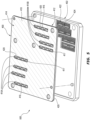
- FIG. 6 is a perspective view illustrating how antenna/absorber piece 400 is coupled with the adjacent waveguide piece 402.
- Waveguide piece 402 may define-in some cases integrally define by way of a casting, for example, or the like-one or more waveguides.
- waveguides are defined comprising notches 424 that are positioned in between adjacent ridges and which may further comprise an opening or slot extending from the upper surface shown in FIG. 5 to the lower surface of waveguide piece 402, the features of which are not shown in FIG. 5 .
- Waveguide piece 402 may, in some embodiments, comprise a casting, such as a casting comprising a Zinc or other suitable preferably metal or metallic material. However, in other contemplated embodiments, waveguide piece 402 may comprise a plastic or other material. In some such embodiments, metallic inserts, coatings, or the like may be used if desired, such as conductive coatings positioned on certain elements of the assembly 500, such as posts 422. In typical sensor assemblies, which, as previously mentioned, may be configured specifically for use in connection with vehicles, other structures may be combined with antenna/absorber piece 400 and waveguide piece 402, such as radomes, electronic components to generate the electromagnetic signals, and the like.
- the waveguide part 402 comprises a metallic block
- the antenna part 400 comprises a plate 400 coupled to the metallic block
- the plate 400 comprises an electrically conductive coating 420 at least substantially covering the plate 400 on a side 412 facing the metallic block.
- the electrically conductive coating 120, 220, 420 is applied to each wall defining each of the antenna slots 215A/215B, 416. According to some further aspects, the electrically conductive coating 120, 220, 420 comprises an electroplated, metallic coating.
Landscapes
- Engineering & Computer Science (AREA)
- Computer Security & Cryptography (AREA)
- Radar, Positioning & Navigation (AREA)
- Remote Sensing (AREA)
- Waveguide Aerials (AREA)
Abstract
Description
- Disclosed herein are various embodiments of sensor assemblies, such as RADAR sensor assemblies for vehicles. In some embodiments, sensor assemblies disclosed herein comprise an antenna portion and/or piece comprising dual properties and/or materials, which may allow for combining the functionality of an electromagnetic absorber with that of an antenna.
- In some embodiments, this combination may be achieved by forming certain portions of the sensor/antenna/waveguide assembly from a suitable lossy and/or absorptive material configured to cancel or at least reduce electromagnetic signal reflection interference and applying an electrically conductive coating to certain regions of the assembly, such as to the regions defining antenna slots, regions adjacent to the antenna slots, and/or other regions in which electrical conductivity is needed or desired.
- In some embodiments, the antenna slots may be formed in a separate piece and/or layer, such as to an antenna plate configured to be coupled with a separate waveguide piece of the assembly. This piece may be made up of, either wholly or partially, a suitable lossy and/or absorptive material configured to reduce electromagnetic interference caused by, for example, fascia reflections. Selected portions of this separate piece may then be electroplated, coated, and/or treated with a suitable metal or other electrically conductive material. For example, in some embodiments, the walls defining antenna slots in the antenna piece may be treated with such a metal or other conductive material layer, which may be helpful in improving performance in near field regions. In some embodiments, other regions of the antenna plate/piece may be treated, such as in some cases an entire surface and/or side of the plate that is configured to be coupled with a waveguide piece of the assembly.
- In other embodiments, the entire assembly, or at least a larger part of the assembly comprising both antenna and waveguide features, may be formed from a unitary, single structure, such as a molded piece, casting, or the like, for example. In some such embodiments, this piece may be molded from the aforementioned absorptive and/or lossy material and then selectively coated and/or treated with the aforementioned conductive material(s) in regions where conductivity may be needed or desired. For example, the regions defining the antenna slots may, in such embodiments, may be so treated/coated, in some cases along with adjacent regions. Other regions, such as posts or other structures defining the waveguides, may also be treated/coated, if desired.
- In a particular example of a vehicle sensor according to some embodiments, the assembly may comprise a waveguide part and an antenna part operably coupled with the waveguide part. In some embodiments, the antenna part may comprise an array of antenna slots, wherein each of the antenna slots is configured to deliver electromagnetic radiation from the waveguide part therethrough. The antenna part may be at least partially defined by a lossy and/or absorptive material configured to reduce electromagnetic radiation reflections. The antenna part may further comprise an electrically conductive and/or metallic coating, which may be applied to the absorptive material of the antenna part, at least in part, to provide desired properties in these regions.
- In some embodiments, the waveguide part may comprise a first layer of the assembly, such as a plate, for example, and the antenna part may comprise a second layer of the assembly, such as a molded piece, coupled to the first layer. In some such embodiments, the electrically conductive and/or metallic coating may be applied to an entire surface, or at least substantially an entire surface, of an inner side of the second layer adjacent to the first layer. In some embodiments, however, the electrically conductive and/or metallic coating may be applied only partially to an outer side of the second layer. In some embodiments, the electrically conductive coating may be applied to a region of the outer side of the second layer adjacent to one or more, or in some cases each, of the antenna slots.
- In some embodiments, the waveguide part may comprise an array of waveguide grooves. In some such embodiments, the antenna part and the array of waveguide grooves may both be part of an integrally formed mold and/or casting. In some such embodiments, each waveguide groove of the array of waveguide grooves may be formed by two or more opposing rows of posts formed in the mold/casting. In some such embodiments, the electrically conductive coating may be applied to each of the posts.
- In some embodiments, at least a subset of the antenna slots may comprise an array of staggered antenna slot arrays each comprising a first row of antenna slots extending along a first line and a second row of antenna slots extending along a second line and offset from the first row of antenna slots. In some such embodiments, the electrically conductive coating may be applied to walls defining each antenna slot of each staggered antenna slot array. In some cases, this coating may be applied so as to wholly cover each of these walls.
- In some embodiments, each of the staggered antenna slot arrays may be positioned in a respective bounded region of the antenna part in which each slot of each staggered antenna slot array is wholly contained. In some such embodiments, the electrically conductive coating may be applied to each of the bounded regions of the antenna part.
- In some embodiments, the waveguide part may comprise a metallic block and/or the antenna part may comprise a plate coupled to the metallic block. In some such embodiments, the plate may comprise an electrically conductive coating at least substantially covering the plate on a side facing the metallic block.
- In some embodiments, the electrically conductive and/or metallic coating may be applied to each wall defining each of the antenna slots.
- In some embodiments, the electrically conductive and/or metallic coating may comprise an electroplated coating.
- The features, structures, steps, or characteristics disclosed herein in connection with one embodiment may be combined in any suitable manner in one or more alternative embodiments.
- Non-limiting and non-exhaustive embodiments of the disclosure are described, including various embodiments of the disclosure with reference to the figures, in which:
-
FIG. 1 is a cross-sectional view of an antenna/absorber piece, which may comprise part of a RADAR sensor assembly according to some embodiments; -
FIG. 2 is a top view of a RADAR sensor assembly according to other embodiments; -
FIG. 3 is bottom view of the RADAR sensor assembly ofFIG. 2 ; -
FIG. 4 depicts an antenna/absorber plate according to other embodiments, which may be coupled with a waveguide piece of a RADAR sensor assembly; -
FIG. 5 is an exploded view of the antenna/absorber plate ofFIG. 4 and an adjacent waveguide piece; and -
FIG. 6 is a perspective view of the complete RADAR sensor assembly ofFIG. 5 . - A detailed description of apparatus, systems, and methods consistent with various embodiments of the present disclosure is provided below. While several embodiments are described, it should be understood that the disclosure is not limited to any of the specific embodiments disclosed, but instead encompasses numerous alternatives, modifications, and equivalents. In addition, while numerous specific details are set forth in the following description in order to provide a thorough understanding of the embodiments disclosed herein, some embodiments can be practiced without some or all of these details. Moreover, for the purpose of clarity, certain technical material that is known in the related art has not been described in detail in order to avoid unnecessarily obscuring the disclosure.
- The embodiments of the disclosure may be best understood by reference to the drawings, wherein like parts may be designated by like numerals. It will be readily understood that the components of the disclosed embodiments, as generally described and illustrated in the figures herein, could be arranged and designed in a wide variety of different configurations. Thus, the following detailed description of the embodiments of the apparatus and methods of the disclosure is not intended to limit the scope of the disclosure, as claimed, but is merely representative of possible embodiments of the disclosure. In addition, the steps of a method do not necessarily need to be executed in any specific order, or even sequentially, nor need the steps be executed only once, unless otherwise specified. Additional details regarding certain preferred embodiments and implementations will now be described in greater detail with reference to the accompanying drawings.
-
FIG. 1 depicts a cross-sectional view of a waveguide/sensor assembly 100, or a portion thereof, such as a RADAR sensor assembly for a vehicle. In this figure, aportion 110 of theassembly 100 preferably comprising an absorber or an absorptive material is shown making up the bulk/core of the portion of theassembly 100 depicted in the figure. - A series of
antenna slots 115 extend throughportion 110. Although not shown inFIG. 1 , eachantenna slots 115 would typically be operably coupled with a waveguide, such as, for example, a waveguide comprising waveguide grooves. Thus, as described in greater detail below, in some embodiments,assembly 100 may comprise only a selected portion of a larger waveguide and/or antenna assembly, such as a plate and/or layer of such a larger assembly with another portion of the larger assembly defining the waveguides. Alternatively,assembly 100 may comprise a single, unitary, and/or self-contained assembly that itself defines the waveguides. More specific examples of both of these embodiments will be described in greater detail in connection with other figures below. - In preferred embodiments, the absorptive material making up
portion 110 may comprise a lossy material configured to absorb electromagnetic radiation/signals, such as RADAR signals. Thus, in some such embodiments, this lossy material may have a dielectric constant of between about 4 and about 12. In some such embodiments, the dielectric constant may be between about 6 and about 9. In a very specific example of a preferred embodiment, the dielectric constant may be about 8. - In other preferred embodiments, the absorptive material may comprise a lossy material having a dielectric constant of between about 6 and about 14. In some such embodiments, the dielectric constant may be between about 9 and about 14 or between about 6 and about 9.
- In preferred embodiments, either in addition to having a preferred dielectric constant or instead of having a preferred dielectric constant, the absorptive material of portion 110 (and other similar absorptive portions/pieces disclosed herein) may have a dielectric loss tangent of between about 0.1 and about 0.7. More preferably, the dielectric loss tangent of the material may be between about 0.15 and about 0.65. In some such embodiments, the dielectric loss tangent of the material may be between about 0.3 and about 0.6, or more preferably between about 0.5 and about 0.6. In a very specific example of a preferred embodiment, the dielectric loss tangent of the material may be about 0.56.
- In other preferred embodiments, either in addition to having a preferred dielectric constant or instead of having a preferred dielectric constant, the absorptive material may have a dielectric loss tangent of between about 0.2 and about 0.6. In some such embodiments, the dielectric loss tangent of the material may be between about 0.3 and about 0.6, or between about 0.2 and about 0.3. Moreover, it should be understood that, within a given design, one or both of these parameters (dielectric constant and/or dielectric loss tangent) may vary within about +/- 20%.
- The lossy and/or absorptive material of
assembly 100 has an electricallyconductive coating 120, such as a metallic coating in preferred embodiments. In the depicted embodiment,metallic coating 120 extends along each of the walls defining each of thevarious antenna slots 115. In addition, in the depicted embodiment, the entire side/surface ofportion 110 on afirst side 112 ofassembly 100 comprisesmetallic coating 120. Asecond side 114 ofassembly 100 opposite fromfirst side 112 only partially comprisesmetallic coating 120, with thecoating 120 extending alongside 114 only in the regions adjacent to theantenna slot 115 openings. - In some embodiments, the conductive and/or
metallic coating 120 may comprise, for example, Copper, Nichrome, Aluminium, Silver, or Zinc. As those of ordinary skill in the art will appreciate, different coating materials may be more suitable for specific processes, applications, and/or functions. - Although in the embodiments of
FIG. 1 andFIG. 2 , thecoating 120/220 is applied only partially betweenadjacent slots 115/215A/215B, in alternative embodiments, this coating may instead be applied continuously from slot to slot. Similarly, in other embodiments, the coating may be applied only along the slot walls and need not be applied between the slots along the adjacent surface(s) at all, allowing absorptive material to wholly extend between and around the slots along the adjacent surfaces, such as the upper and/or lower surface. - However, in embodiments in which the coating extends beyond the region defining the slots, preferably the coating extends symmetrically in this adjacent region, such as in the adjacent surface (
surface 114 inFIG. 1 and the surface depicted inFIG. 2 , for example). In some such embodiments, the coating may at least extend symmetrically along the azimuth plane in this area. For example, in the embodiment ofFIG. 2 , preferably thecoating 220 extends symmetrically along the long sides of theslots 215A and/or 215B, as shown inFIG. 2 , due to the higher influence on the antenna near fields in these regions. - As will be best understood by those of ordinary skill in the art after reviewing additional details and embodiments provided below, various alternative embodiments are contemplated in which the
coating 120 is selectively applied only in regions where required or reasonably necessary, such as parts/portions requiring electrical conductivity. Thus, using the example ofFIG. 1 , by providing ametallic coating 120 that extends entirely along one surface, this surface may contact an adjacent waveguide portion of the assembly. By using a lossy/absorptive material for the base/core of assembly/piece 100 and selectively providing ametallic coating 120 in this manner, the antenna function and the absorber function, which are typically provided by two separate pieces of a RADAR/sensor assembly, may be combined or integrated into one piece. - In preferred embodiments, conductive and/or
metallic coating 120 may comprise an electroplated coating. However, in other embodiments and related implementations, coating 120 may be applied in other ways, such as using, for example, metal patterning, metal deposition, and/or photolithography. In other embodiments and/or implementations, conductive and/or metallic coatings may be applied using, for example, physical vapor deposition (PVD) processes, which may include sputter deposition (sputtering) and evaporation. - In some embodiments and implementations, the coating process may include the use of plasma cleaning in order to give a clean surface for the coating to be applied on. For example, a thin adhesive layer of chromium may be sputtered in order to improve the adhesion between absorber material and the conductive and/or metallic coating.
- As another example, in some embodiments and implementations, selective plating (partially coating) may be applied by creating a pattern on a mask. This process may involve chemical etching, micromachining, and/or photolithography. A mask for this purpose may be, for example, a glass plate patterned with chromium on one side. In the case of photolithography, by projecting UV light onto the mask, the pattern may be printed to the photoresist, since glass is transparent under UV light while chromium is opaque. Another potentially suitable approach may involve plating the structure and then creating a negative pattern on the mask, which may then be subject to an etching process again.
- By providing a metamaterial or other material having an absorptive material and selectively applied and/or tuned conductive materials in desired regions, absorption properties, such as absorption for reflection cancellation due to, for example, fascia reflections, may be achieved without unduly impacting antenna performance, which often happens when an absorptive material is used in regions close to the antennae near field(s). In other words, by providing artificial properties on an absorptive type of material, the principles disclosed herein may allow for engineering electromagnetic properties in such a way that cannot be exhibited by conventional materials. An absorber with such features and/or characteristics may thereby utilize its effective complex permittivity and permeability to address various issues present in, for example, vehicle antennae/sensors, such as reflection cancellation, while minimizing or at least reducing antenna performance.
- It should be understood that a wide variety of alternative configurations are contemplated and/or would be available to those of ordinary skill in the art after having received the benefit of this disclosure. For example, in some embodiments, the walls defining
antenna slots 115 may only be partially covered with a suitable electroplating or otherconductive material 120. Similarly, someantenna slots 115 in certain configurations may be left without any such conductive layer. - In addition, some embodiments may be configured such that
side 112 has certain portions that lackconductive layer 120 such that theabsorptive material 110 is exposed. Similarly, some embodiments may comprise noconductive layer 120 alongside 114, or may comprise a larger portion of thisside 114 withconductive layer 120 depending upon, for example, the spacing of the antenna slots, the desired use of the antenna/sensor, etc. -
FIGS. 2 and3 depict opposite sides, respectively, of an embodiment of a waveguide/sensor assembly 200, or a portion thereof, according to another embodiment. The waveguide/sensor assembly 200 can be regarded as a vehicle sensor assembly.FIG. 2 depicts a first side ofassembly 200, which includes a first array ofantenna slots 215A and a second array ofantenna slots 215B. In some embodiments, array ofantenna slots 215A may comprise an RX section andantenna slots 215B may comprise a TX section of theassembly 200. - Similarly,
respective waveguide grooves 218A/218B may be formed, which may direct electromagnetic radiation to and/or from one or morerespective antenna slots 215A/215B.The grooves 218A/218B may according to some aspects constitute a waveguide part. -
RX slots 215A comprise elongated, straight slots, whereasTX slots 215B comprise curved or "wavy" slots that, as shown inFIG. 2 , oscillate back and forth between opposing sides of an elongated axis.TX slots 215B further comprise an optional phase-compensating feature. In the depicted embodiment, this is accomplished by applying one or more angled and/or tapered sections, such as tapered grooves or cutouts, along the slots. Thus, the depicted embodiment illustrates a tapered and/or angled section/surface that is formed along both opposing sidewalls defining eachantenna slot 215B at points of maxima for the oscillating pattern of the respective slot. - These tapering sections may comprise a stepped taper or ledge or may comprise a smoothly transitioning taper. In other words, a ledge may be formed at the starting point of the taper and therefore, rather than a smooth taper between the outer surface of the structure defining the
slot 215B and the starting point of the tapering section, the transition of the tapering section may be immediate from the starting point, which is at a ledge of section to the outer surface of the structure forming the slot. - In some embodiments, all of the peaks/maxima of the oscillating pattern of
slots 215B may comprise a phase-compensating feature. Alternatively, in some embodiments, only a subset of the peaks/maxima defined byslots 215B may comprise such a feature. Of course, in still other embodiments, no such phase-compensating feature may be included at all. - In addition, in some embodiments in which
slots 215B intermittently oscillate on opposite sides of its respective elongated axis and/or adjacent waveguide along at least a portion thereof, each of at least a subset of the plurality of the tapering surfaces/sections may be spaced apart in a manner that coincides with the intermittent oscillation of theslots 215B. In some such embodiments, all of the tapering surfaces/sections may be spaced apart in a manner that coincides with the intermittent oscillation of theslots 215B. - It should be understood, however, that the stepped taper of
assembly 200 is but an example for purposes of illustration and that a wide variety of alternative embodiments are contemplated. For example, although only a single step is used in the tapered section ofassembly 200, any number of steps may be used in between the one step shown in this embodiment and an effectively infinite number of steps involved in a smooth taper. - Each of the tapering sections of
assembly 200 may comprise a stepped taper extending between a first edge of the ledge formed by the tapering section, which first edge may be positioned in between the external surface of thestructure forming slots 215B and the internal surface of this structure, and a second edge of a concavely curved surface (in some cases, a semi-circular concavely curved surface), the second edge extending along the external surface of the aforementioned structure. Again, any number of intermediate steps may be used as desired. - In preferred embodiments, these sections/surfaces may be positioned so as to alternate and be staggered along the opposing slot sidewalls such that each section is positioned at a particular point along the axis of along only one sidewall of each
respective slot 215B. In addition, even more preferably, each section may be formed along one of the peaks of each oscillatingrespective slot 215B. Thus, for example, if the antenna slot defines, or at least substantially defines, a sine wave, each of the tapering/phase-compensating sections is preferably formed along one of the peaks of the sine wave extending towards the axial center of theslot 215B and/or accompanying waveguide. - In some embodiments, all of the aforementioned peaks may comprise a phase-compensating feature. Alternatively, only a subset of the peaks defined by each
respective slot 215B may comprise such a feature. - In some embodiments, each
respective slot 215B may intermittently oscillate on opposite sides of the elongated axis of eachrespective slot 215B and/or adjacent waveguide along at least a portion thereof. In some such embodiments, each of at least a subset of the plurality of the tapering surfaces/sections may be spaced apart in a manner that coincides with the intermittent oscillation of eachrespective slot 215B. In some such embodiments, all of the tapering surfaces/sections may be spaced apart in a manner that coincides with the intermittent oscillation of eachrespective slot 215B. - Thus, for example, in some embodiments, each of the plurality of tapering sections surfaces may comprise a first set of tapering surfaces on a first side of each
respective slot 215B and a second set of tapering surfaces on a second side of eachrespective slot 215B opposite the first side. Preferably, the tapering surfaces/sections alternate such that each tapering surface of first set of tapering surfaces is positioned adjacent to one or more tapering surfaces of the second set of tapering surfaces along the axis of eachrespective slot 215B and each tapering surface of the second set of tapering surfaces is positioned adjacent to one or more tapering surfaces of the first set of tapering surfaces along the axis, again, preferably alternating back and forth across eachrespective slot 215B. - Each of the plurality of tapering surfaces/sections may comprise a curved, tapering surface, as shown in
FIG. 2 . Indeed, in the depicted embodiment, each of the tapering surfaces/sections is defined, at least in part, by a semi-circular cutout, which may be formed at the exterior surface of eachrespective slot 215B, as a concave region from the convex region of the curve defined by eachrespective slot 215B, and then may taper down to a corner, edge, or starting point of the taper. Thus, preferably, the tapers of one or more (or each) of the tapering sections do not extend all the way between opposing surfaces of the structure ofassembly 200 definingslots 215B, but rather start at a point between the opposing surfaces of this structure and extend to the upper/outer portion ofslots 215B on the side opposite the aforementioned waveguides, which are on the opposite side ofassembly 200, as shown inFIG. 3 . - However, in embodiments in which one or more of the tapering sections has a starting point between opposing surfaces of the structure defining the slot(s) 215B, it may be desirable from a manufacturing standpoint that the starting point(s) of the tapering sections be sufficiently spaced from the (typically inner) surface from which the slot(s) 215B originates. Thus, in some embodiments, the starting point may be located at a point no less than 20%, or no less than about 20%, of the distance from the lower/inner and/or originating surface of the slot(s) to the upper/outer and/or terminating surface of the slot(s).
- Other embodiments are contemplated in which the tapering surfaces/sections may instead be straight or non-curved. In addition, in some embodiments, the curvature of the tapering sections may extend in multiple dimensions. In other words, a semi-spherically curved surface may be formed within one or more of these tapering sections if desired. Additional details regarding these phase-compensating features can be found in
U.S. Patent Application Serial No. 17/370,922 titled PHASE-COMPENSATED WAVEGUIDES AND RELATED SENSOR ASSEMBLIES, the entire contents of which are hereby incorporated by reference herein. - Preferably, each of the various antenna slots, including both
RX slots 215A andTX slots 215B, is defined and/or coated, wholly or at least in part, by an electrically conductive plating/coating/layer 220. Although the walls defining these slots are not shown inFIG. 2 , in the depicted embodiment, thisconductive material 220 also extends adjacent to each of theslots 215A/215B on the adjacent surface, as shown inFIG. 2 . The material making upassembly 200 otherwise may comprise anabsorptive material 210, which may comprise any of the absorptive materials mentioned herein. -
FIG. 3 depicts assembly 200 from the side opposite to that ofFIG. 2 . On this side, the waveguide structures of theassembly 200 are depicted. More particularly, several rows ofposts 222 are depicted. In between two or more rows of posts on each opposing side, a series of waveguides are defined. Of course, in alternative embodiments, waveguides may be defined in between a single row of posts on each side or waveguides may be defined in other ways, such as trench-style waveguides lacking posts altogether. - In addition to coating or otherwise applying the
conductive material layer 220 to the walls definingantenna slots conductive material layer 220 may also be applied to each of theposts 222, either wholly or in part (such as on each top surface of each post 222). As shown inFIG. 3 , however, some embodiments, including the depicted embodiment, may comprise an electroplating or other conductive layer/coating 220 applied to other regions of the waveguide side of theassembly 200. For example, in the depicted embodiment, all of theposts 222 are conductively coated in their entireties, along with the adjacent waveguide regions. In some embodiments, the entire surface defining the waveguides may be coated with a suitable electrically conductive material. However, as shown inFIG. 3 , in some embodiments, certain regions of theassembly 200 not requiring conductivity and/or that may benefit from exposed absorptive materials need not be coated/layered withmaterial 220. -
FIGS. 4-6 depict another antenna and/or sensor assembly according to still other embodiments. In this embodiment, a separate plate or other piece is used for the antenna slots of the assembly. This separate piece is preferably formed, in some cases wholly formed (aside from the conductive coating(s)/cover(s)/treatment(s) discussed below), from a suitable absorptive material, including any of those discussed elsewhere herein. The separate antenna/absorber piece may then be treated in selected regions with a metal or other electrically conductive material, including any of those materials discussed herein. - In preferred embodiments and related implementations, this treatment comprises an electroplating of a metal in the regions defining the sidewalls of the antenna slots. In some cases, this treatment comprises further coating of adjacent regions of the antenna/absorber piece, such as regions extending along an upper surface of the piece adjacent to the antenna slots in the case of the piece being a plate. Similarly, the lower side/surface of the assembly may be treated/coated, in some cases so as to encompass the entire lower side/surface, to facilitate desired coupling with the requisite electrical contact with another piece/layer of the assembly. Thus, in the case of the antenna/absorber piece being a plate, the entire lower surface may be treated/coated, or at least substantially entirely treated/coated, with the desired conductive material(s).
- In
FIG. 4 , an antenna plate orpiece 400, generally anantenna part 400, but more particularly anantenna plate 400 in the depicted embodiment, is shown. As described in greater detail below,antenna plate 400 defines the antenna slots of the assembly and may be coupled with one or more other elements to complete the assembly, such as awaveguide piece 402, generally awaveguide part 402, shown inFIGS. 5 and6 . Preferably, the antenna/absorber piece 400 comprises-in some cases wholly comprises aside from the conductive materials described below-anabsorptive material 410, which may, for example, reduce signal degradation due to reflection from fascia materials of a vehicle and the like by absorbing such reflected signals. According to some aspects, thewaveguide part 402 comprises afirst layer 402 of avehicle sensor assembly 500 having multiple layers and theantenna part 400 comprises a second and/orupper layer 400 of theassembly 500 coupled to thefirst layer 402. - Alternatively, as described above and depicted in the embodiment of
FIGS. 2 and3 , thewaveguide part 218A/218B andantenna part 205 may be defined as respective portions of a larger, unitary piece, such asassembly 200. In this case, for example, the waveguide part may comprise, at least in part, one or more waveguide grooves, such aswaveguide grooves 218A/218B, and theantenna part 205 of the assembly may compriseantenna slots 215A/215B. According to some aspects, thewaveguide part 218A/218B comprises an array ofwaveguide grooves 218A/218B), and theantenna part 205 and the array ofwaveguide grooves 218A/218B are both part of an integrally formed casting. According to some further aspects, eachwaveguide groove 218A/218B of the array ofwaveguide grooves 218A/218B is formed by two or more opposing rows ofposts 222 formed in the casting. - A series of antenna slot arrays may be formed in antenna/
absorber piece 400. In some embodiments, these antenna slot arrays may, as mentioned above, be divided into transmission and receiving antenna slot arrays. Thus, in the depicted embodiment ofFIGS. 4-6 , a first array ofantenna slot arrays 415A, which may compriseRX antenna slots 416 is provided and a second array ofantenna slot arrays 415B, which may compriseTX antenna slots 416, is provided at a region preferably maximally, or at least substantially maximally, spaced apart from the RXantenna slot arrays 415A on the antenna/absorber piece 400. - Unlike the antenna slots of the embodiments previously discussed,
antenna slot arrays antenna slots 416. Thus,arrays 415A each comprises a plurality of relativelyshorter antenna slots 416 extending in two rows offset with respect to one another. As also shown inFIG. 4 , some of the arrays themselves may be offset with respect to one another. Similarly,arrays 415B may comprise staggeredantenna slots 416 extending in two offset rows and eachindividual array 415B may be offset from one or moreadjacent arrays 415B (although somesuch arrays 415B may be aligned, as is the case with the first twosuch arrays 415B). According to some aspects, at least a subset of theantenna slots 215A/215B, 416 is defined in an array of staggeredantenna slot arrays 415A/415B each comprising a first row ofantenna slots 416 extending along a first line and a second row ofantenna slots 416 extending along a second line and offset from the first row ofantenna slots 416. - In the depicted embodiment, each of the individual arrays of
antenna slots 416 in botharrays region 417 in which each of theslots 416 of eachsuch array 415A/415B is wholly contained. In the depicted embodiment, each of theseaforementioned regions 417 is treated, such as electroplated, with a conductive material, which may comprise any of the conductive materials mentioned herein. According to some aspects, each of the staggeredantenna slot arrays 415A/415B is positioned in a respective boundedregion 417 of theantenna part 400 in which eachslot 416 of each staggeredantenna slot array 415A/415B is wholly contained, and wherein the electricallyconductive coating 420 is further applied to each of thebounded regions 417 of theantenna part 400. - Preferably, this treatment also extends, at least partially, but preferably wholly, within each of the
individual slots 416 within each staggeredslot array 415A/415B. Although each of theaforementioned regions 417 is recessed from an adjacentouter side 414, it is contemplated that alternative embodiments need not comprise recessed regions. Rather, boundedregions 417 containing all, or substantially all, of thestaggered slots 416 may instead be formed by extending the electroplated or otherwise treated regions within a desired region about each of thevarious slots 416, which region may but need not necessarily have a shape identical or similar to the recessedregions 417 depicted inFIG. 4 . - An
inner side 412 of antenna/absorber piece 400, which is opposite to theouter side 414, may be electroplated, coated, or otherwise treated with aconductive material 420 that according to some aspects constitutes an electrically conductive coating, such as any of those materials mentioned herein. In some embodiments, the entire surface of theinner side 412 may be treated in this manner. However, alternative embodiments are contemplated in which this side may only be treated in certain areas as needed. According to some aspects, the electricallyconductive coating 420 is applied only partially to theouter side 414 of thesecond layer 400. According to some aspects, the electricallyconductive coating 420 is applied to a region of theouter side 414 of thesecond layer 400 adjacent to each of theantenna slots 416. According to some aspects, the electricallyconductive coating 420 is applied to walls defining eachantenna slot 416 of each staggeredantenna slot array 415A/415B. According to some further aspects, the electricallyconductive coating 420 is applied to entire surfaces of each of the walls defining eachantenna slot 416 of each staggeredantenna slot array 415A/415B. -
FIG. 5 is an exploded view depicting a morecomplete assembly 500 including antenna/absorber piece 400 and anadjacent waveguide piece 402 andFIG. 6 is a perspective view illustrating how antenna/absorber piece 400 is coupled with theadjacent waveguide piece 402.Waveguide piece 402 may define-in some cases integrally define by way of a casting, for example, or the like-one or more waveguides. - Although a wide variety of alternative embodiments are contemplated and/or would be apparent to those ordinary skill in the art after having received the benefit of this disclosure, in the depicted embodiment, waveguides are defined comprising
notches 424 that are positioned in between adjacent ridges and which may further comprise an opening or slot extending from the upper surface shown inFIG. 5 to the lower surface ofwaveguide piece 402, the features of which are not shown inFIG. 5 . - Portions of these waveguides may, as also shown in
FIG. 5 , be defined by a series ofposts 422. These waveguide structures, ridges, and/ornotches 424 may be formed or otherwise disposed on both sides of antenna/absorber piece 400, if desired/needed.Waveguide piece 402 may, in some embodiments, comprise a casting, such as a casting comprising a Zinc or other suitable preferably metal or metallic material. However, in other contemplated embodiments,waveguide piece 402 may comprise a plastic or other material. In some such embodiments, metallic inserts, coatings, or the like may be used if desired, such as conductive coatings positioned on certain elements of theassembly 500, such as posts 422. In typical sensor assemblies, which, as previously mentioned, may be configured specifically for use in connection with vehicles, other structures may be combined with antenna/absorber piece 400 andwaveguide piece 402, such as radomes, electronic components to generate the electromagnetic signals, and the like. - According to some aspects, the
waveguide part 402 comprises a metallic block, wherein theantenna part 400 comprises aplate 400 coupled to the metallic block, and theplate 400 comprises an electricallyconductive coating 420 at least substantially covering theplate 400 on aside 412 facing the metallic block. - According to some aspects, the electrically
conductive coating antenna slots 215A/215B, 416. According to some further aspects, the electricallyconductive coating - It should be understood that whereas preferred embodiments may be used in connection with vehicle sensors, such as vehicle RADAR modules or the like, the principles disclosed herein may be used in a wide variety of other contexts, such as other types of RADAR assemblies, including such assemblies used in aviation, maritime, scientific applications, military, and electronic warfare. Other examples include point-to-point wireless links, satellite communication antennas, other wireless technologies, such as 5G wireless, and high-frequency test and scientific instrumentation. Thus, the principles disclosed herein may be applied to any desired communication sub-system and/or high-performance sensing and/or imaging systems, including medical imaging, security imaging and stand-off detection, automotive and airborne radar and enhanced passive radiometers for earth observation and climate monitoring from space.
- The foregoing specification has been described with reference to various embodiments and implementations. However, one of ordinary skill in the art will appreciate that various modifications and changes can be made without departing from the scope of the present disclosure. For example, various operational steps, as well as components for carrying out operational steps, may be implemented in various ways depending upon the particular application or in consideration of any number of cost functions associated with the operation of the system. Accordingly, any one or more of the steps may be deleted, modified, or combined with other steps. Further, this disclosure is to be regarded in an illustrative rather than a restrictive sense, and all such modifications are intended to be included within the scope thereof. Likewise, benefits, other advantages, and solutions to problems have been described above with regard to various embodiments. However, benefits, advantages, solutions to problems, and any element(s) that may cause any benefit, advantage, or solution to occur or become more pronounced, are not to be construed as a critical, a required, or an essential feature or element.
- Those having skill in the art will appreciate that many changes may be made to the details of the above-described embodiments without departing from the underlying principles of the invention. The scope of the present inventions should, therefore, be determined only by the following claims.
Claims (15)
- A vehicle sensor assembly (200, 500), comprising:a waveguide part (218A/218B, 402); andan antenna part (205, 400) operably coupled with the waveguide part (218A/218B, 402), wherein the antenna part (205, 400) comprises an array of antenna slots (215A/215B, 416), and wherein each of the antenna slots (215A/215B, 416) is configured to deliver electromagnetic radiation from the waveguide part (218A/218B, 402) therethrough,characterized in that the antenna part (205, 400) is at least partially defined by an absorptive material (110, 210, 410) configured to reduce electromagnetic radiation reflections, and wherein the antenna part (205, 400) further comprises an electrically conductive coating (120, 220, 420).
- The vehicle sensor assembly (200, 500) of claim 1, wherein the waveguide part (402) comprises a first layer (402) of the assembly (200, 500), and wherein the antenna part (400) comprises a second layer (400) of the assembly (200, 500), coupled to the first layer (402).
- The vehicle sensor assembly (200, 500) of claim 2, wherein the electrically conductive coating (120, 220, 420) is applied to an entire surface of an inner side (412) of the second layer (400) adjacent to the first layer (402).
- The vehicle sensor assembly (200, 500) of claim 2 or claim 3, wherein the electrically conductive coating (120, 220, 420) is applied only partially to an outer side (414) of the second layer (400).
- The vehicle sensor assembly (200, 500) of any of claims 2-4, wherein the electrically conductive coating (120, 220, 420) is applied to a region of the outer side (414) of the second layer (400) adjacent to each of the antenna slots (416).
- The vehicle sensor assembly (200, 500) of claim 1, wherein the waveguide part (218A/218B) comprises an array of waveguide grooves (218A/218B), and wherein the antenna part (205) and the array of waveguide grooves (218A/218B) are both part of an integrally formed casting.
- The vehicle sensor assembly (200, 500) of claim 6, wherein each waveguide groove (218A/218B) of the array of waveguide grooves (218A/218B) is formed by two or more opposing rows of posts (222) formed in the casting.
- The vehicle sensor assembly (200, 500) of claim 7, wherein the electrically conductive coating (220) is applied to each of the posts (222).
- The vehicle sensor assembly (200, 500) of any of claims 1-8, wherein at least a subset of the antenna slots (215A/215B, 416) is defined in an array of staggered antenna slot arrays (415A/415B) each comprising a first row of antenna slots (416) extending along a first line and a second row of antenna slots (416) extending along a second line and offset from the first row of antenna slots (416).
- The vehicle sensor assembly (200, 500) of claim 9, wherein the electrically conductive coating (420) is applied to walls defining each antenna slot (416) of each staggered antenna slot array (415A/415B).
- The vehicle sensor assembly (200, 500) of claim 10, wherein the electrically conductive coating (420) is applied to entire surfaces of each of the walls defining each antenna slot (416) of each staggered antenna slot array (415A/415B).
- The vehicle sensor assembly (200, 500) of any of claims 9-11, wherein each of the staggered antenna slot arrays (415A/415B) is positioned in a respective bounded region (417) of the antenna part (400) in which each slot (416) of each staggered antenna slot array (415A/415B) is wholly contained, and wherein the electrically conductive coating (420) is further applied to each of the bounded regions (417) of the antenna part (400).
- The vehicle sensor assembly (200, 500) of claim 1, wherein the waveguide part (402) comprises a metallic block, wherein the antenna part (400) comprises a plate (400) coupled to the metallic block, and wherein the plate (400) comprises an electrically conductive coating (420) at least substantially covering the plate (400) on a side (412) facing the metallic block.
- The vehicle sensor assembly (200, 500) of any of claims 1-13, wherein the electrically conductive coating (120, 220, 420) is applied to each wall defining each of the antenna slots (215A/215B, 416).
- The vehicle sensor assembly (200, 500) of any of claims 1-14, wherein the electrically conductive coating (120, 220, 420) comprises an electroplated, metallic coating.
Priority Applications (3)
| Application Number | Priority Date | Filing Date | Title |
|---|---|---|---|
| EP22215894.1A EP4391224A1 (en) | 2022-12-22 | 2022-12-22 | Integrated vehicle antenna absorber |
| PCT/EP2023/086720 WO2024133319A1 (en) | 2022-12-22 | 2023-12-19 | Integrated vehicle antenna absorber |
| CN202380078476.4A CN120188339A (en) | 2022-12-22 | 2023-12-19 | Integrated vehicle antenna absorber |
Applications Claiming Priority (1)
| Application Number | Priority Date | Filing Date | Title |
|---|---|---|---|
| EP22215894.1A EP4391224A1 (en) | 2022-12-22 | 2022-12-22 | Integrated vehicle antenna absorber |
Publications (1)
| Publication Number | Publication Date |
|---|---|
| EP4391224A1 true EP4391224A1 (en) | 2024-06-26 |
Family
ID=84568909
Family Applications (1)
| Application Number | Title | Priority Date | Filing Date |
|---|---|---|---|
| EP22215894.1A Pending EP4391224A1 (en) | 2022-12-22 | 2022-12-22 | Integrated vehicle antenna absorber |
Country Status (3)
| Country | Link |
|---|---|
| EP (1) | EP4391224A1 (en) |
| CN (1) | CN120188339A (en) |
| WO (1) | WO2024133319A1 (en) |
Citations (4)
| Publication number | Priority date | Publication date | Assignee | Title |
|---|---|---|---|---|
| US20200036102A1 (en) * | 2018-07-30 | 2020-01-30 | Nidec Corporation | Waveguide device and antenna device |
| WO2021122725A1 (en) * | 2019-12-20 | 2021-06-24 | Gapwaves Ab | An antenna arrangement with a low-ripple radiation pattern |
| US20210247512A1 (en) * | 2020-02-12 | 2021-08-12 | Veoneer Us, Inc. | Vehicle radar sensor assemblies |
| WO2021259674A1 (en) * | 2020-06-23 | 2021-12-30 | Gapwaves Ab | Inline slotted waveguide antenna |
-
2022
- 2022-12-22 EP EP22215894.1A patent/EP4391224A1/en active Pending
-
2023
- 2023-12-19 WO PCT/EP2023/086720 patent/WO2024133319A1/en not_active Ceased
- 2023-12-19 CN CN202380078476.4A patent/CN120188339A/en active Pending
Patent Citations (4)
| Publication number | Priority date | Publication date | Assignee | Title |
|---|---|---|---|---|
| US20200036102A1 (en) * | 2018-07-30 | 2020-01-30 | Nidec Corporation | Waveguide device and antenna device |
| WO2021122725A1 (en) * | 2019-12-20 | 2021-06-24 | Gapwaves Ab | An antenna arrangement with a low-ripple radiation pattern |
| US20210247512A1 (en) * | 2020-02-12 | 2021-08-12 | Veoneer Us, Inc. | Vehicle radar sensor assemblies |
| WO2021259674A1 (en) * | 2020-06-23 | 2021-12-30 | Gapwaves Ab | Inline slotted waveguide antenna |
Also Published As
| Publication number | Publication date |
|---|---|
| CN120188339A (en) | 2025-06-20 |
| WO2024133319A1 (en) | 2024-06-27 |
Similar Documents
| Publication | Publication Date | Title |
|---|---|---|
| US12126081B2 (en) | Oscillating waveguides and related sensor assemblies | |
| US11762087B2 (en) | Vehicle radar sensor assemblies | |
| US11563259B2 (en) | Waveguide signal confinement structures and related sensor assemblies | |
| US9413076B2 (en) | Electromagnetic radiation absorber | |
| US8773323B1 (en) | Multi-band antenna element with integral faraday cage for phased arrays | |
| US20030052810A1 (en) | Device to conceal a radar representing a pattern in relief, equipping especially a vehicle, and detection system comprising such a device | |
| US12283736B2 (en) | PCB tuning for waveguide antennae | |
| EP3216083B1 (en) | Circumferential frame for antenna back-lobe and side-lobe attenuation | |
| WO2024133319A1 (en) | Integrated vehicle antenna absorber | |
| US20030142026A1 (en) | Surface/traveling wave suppressor for antenna arrays of notch radiators | |
| CN102723578B (en) | Satellite antenna for satellite communication in motion | |
| WO2023283148A1 (en) | Phase-compensated waveguides and related sensor assemblies | |
| US20250110202A1 (en) | Automotive sensor module with backscattering cancellation | |
| CN120239830A (en) | Automotive sensor modules with absorbing and/or non-reflective layers | |
| US20250110204A1 (en) | Automotive sensor module with backscattering cancellation | |
| CN205051001U (en) | Super material absorbent structure , protection casing and electronic system | |
| US9520631B2 (en) | Spherical filter | |
| CN110021820B (en) | A radome | |
| JP7799902B2 (en) | Additive Manufacturing Cluster Feed | |
| US20250183547A1 (en) | Electromagnetic-wave absorber and reflector, planar antenna, and method for manufacturing electromagnetic-wave absorber and reflector | |
| KR101874542B1 (en) | Structures supporting beam steering of antenna | |
| CN109904619A (en) | Planar Equiangular Helical Broadband Frequency Selective Surface |
Legal Events
| Date | Code | Title | Description |
|---|---|---|---|
| PUAI | Public reference made under article 153(3) epc to a published international application that has entered the european phase |
Free format text: ORIGINAL CODE: 0009012 |
|
| STAA | Information on the status of an ep patent application or granted ep patent |
Free format text: STATUS: THE APPLICATION HAS BEEN PUBLISHED |
|
| AK | Designated contracting states |
Kind code of ref document: A1 Designated state(s): AL AT BE BG CH CY CZ DE DK EE ES FI FR GB GR HR HU IE IS IT LI LT LU LV MC ME MK MT NL NO PL PT RO RS SE SI SK SM TR |
|
| STAA | Information on the status of an ep patent application or granted ep patent |
Free format text: STATUS: REQUEST FOR EXAMINATION WAS MADE |
|
| 17P | Request for examination filed |
Effective date: 20241120 |
|
| RBV | Designated contracting states (corrected) |
Designated state(s): AL AT BE BG CH CY CZ DE DK EE ES FI FR GB GR HR HU IE IS IT LI LT LU LV MC ME MK MT NL NO PL PT RO RS SE SI SK SM TR |