EP4391060A1 - Display device - Google Patents
Display device Download PDFInfo
- Publication number
- EP4391060A1 EP4391060A1 EP21815093.6A EP21815093A EP4391060A1 EP 4391060 A1 EP4391060 A1 EP 4391060A1 EP 21815093 A EP21815093 A EP 21815093A EP 4391060 A1 EP4391060 A1 EP 4391060A1
- Authority
- EP
- European Patent Office
- Prior art keywords
- compensation
- switch
- resistors
- resistance
- display device
- Prior art date
- Legal status (The legal status is an assumption and is not a legal conclusion. Google has not performed a legal analysis and makes no representation as to the accuracy of the status listed.)
- Pending
Links
Images


Classifications
-
- H—ELECTRICITY
- H10—SEMICONDUCTOR DEVICES; ELECTRIC SOLID-STATE DEVICES NOT OTHERWISE PROVIDED FOR
- H10D—INORGANIC ELECTRIC SEMICONDUCTOR DEVICES
- H10D86/00—Integrated devices formed in or on insulating or conducting substrates, e.g. formed in silicon-on-insulator [SOI] substrates or on stainless steel or glass substrates
- H10D86/40—Integrated devices formed in or on insulating or conducting substrates, e.g. formed in silicon-on-insulator [SOI] substrates or on stainless steel or glass substrates characterised by multiple TFTs
- H10D86/441—Interconnections, e.g. scanning lines
-
- G—PHYSICS
- G09—EDUCATION; CRYPTOGRAPHY; DISPLAY; ADVERTISING; SEALS
- G09G—ARRANGEMENTS OR CIRCUITS FOR CONTROL OF INDICATING DEVICES USING STATIC MEANS TO PRESENT VARIABLE INFORMATION
- G09G3/00—Control arrangements or circuits, of interest only in connection with visual indicators other than cathode-ray tubes
- G09G3/20—Control arrangements or circuits, of interest only in connection with visual indicators other than cathode-ray tubes for presentation of an assembly of a number of characters, e.g. a page, by composing the assembly by combination of individual elements arranged in a matrix no fixed position being assigned to or needed to be assigned to the individual characters or partial characters
-
- G—PHYSICS
- G09—EDUCATION; CRYPTOGRAPHY; DISPLAY; ADVERTISING; SEALS
- G09G—ARRANGEMENTS OR CIRCUITS FOR CONTROL OF INDICATING DEVICES USING STATIC MEANS TO PRESENT VARIABLE INFORMATION
- G09G3/00—Control arrangements or circuits, of interest only in connection with visual indicators other than cathode-ray tubes
- G09G3/20—Control arrangements or circuits, of interest only in connection with visual indicators other than cathode-ray tubes for presentation of an assembly of a number of characters, e.g. a page, by composing the assembly by combination of individual elements arranged in a matrix no fixed position being assigned to or needed to be assigned to the individual characters or partial characters
- G09G3/22—Control arrangements or circuits, of interest only in connection with visual indicators other than cathode-ray tubes for presentation of an assembly of a number of characters, e.g. a page, by composing the assembly by combination of individual elements arranged in a matrix no fixed position being assigned to or needed to be assigned to the individual characters or partial characters using controlled light sources
- G09G3/30—Control arrangements or circuits, of interest only in connection with visual indicators other than cathode-ray tubes for presentation of an assembly of a number of characters, e.g. a page, by composing the assembly by combination of individual elements arranged in a matrix no fixed position being assigned to or needed to be assigned to the individual characters or partial characters using controlled light sources using electroluminescent panels
- G09G3/32—Control arrangements or circuits, of interest only in connection with visual indicators other than cathode-ray tubes for presentation of an assembly of a number of characters, e.g. a page, by composing the assembly by combination of individual elements arranged in a matrix no fixed position being assigned to or needed to be assigned to the individual characters or partial characters using controlled light sources using electroluminescent panels semiconductive, e.g. using light-emitting diodes [LED]
- G09G3/3208—Control arrangements or circuits, of interest only in connection with visual indicators other than cathode-ray tubes for presentation of an assembly of a number of characters, e.g. a page, by composing the assembly by combination of individual elements arranged in a matrix no fixed position being assigned to or needed to be assigned to the individual characters or partial characters using controlled light sources using electroluminescent panels semiconductive, e.g. using light-emitting diodes [LED] organic, e.g. using organic light-emitting diodes [OLED]
- G09G3/3225—Control arrangements or circuits, of interest only in connection with visual indicators other than cathode-ray tubes for presentation of an assembly of a number of characters, e.g. a page, by composing the assembly by combination of individual elements arranged in a matrix no fixed position being assigned to or needed to be assigned to the individual characters or partial characters using controlled light sources using electroluminescent panels semiconductive, e.g. using light-emitting diodes [LED] organic, e.g. using organic light-emitting diodes [OLED] using an active matrix
-
- G—PHYSICS
- G09—EDUCATION; CRYPTOGRAPHY; DISPLAY; ADVERTISING; SEALS
- G09G—ARRANGEMENTS OR CIRCUITS FOR CONTROL OF INDICATING DEVICES USING STATIC MEANS TO PRESENT VARIABLE INFORMATION
- G09G3/00—Control arrangements or circuits, of interest only in connection with visual indicators other than cathode-ray tubes
- G09G3/20—Control arrangements or circuits, of interest only in connection with visual indicators other than cathode-ray tubes for presentation of an assembly of a number of characters, e.g. a page, by composing the assembly by combination of individual elements arranged in a matrix no fixed position being assigned to or needed to be assigned to the individual characters or partial characters
- G09G3/22—Control arrangements or circuits, of interest only in connection with visual indicators other than cathode-ray tubes for presentation of an assembly of a number of characters, e.g. a page, by composing the assembly by combination of individual elements arranged in a matrix no fixed position being assigned to or needed to be assigned to the individual characters or partial characters using controlled light sources
- G09G3/30—Control arrangements or circuits, of interest only in connection with visual indicators other than cathode-ray tubes for presentation of an assembly of a number of characters, e.g. a page, by composing the assembly by combination of individual elements arranged in a matrix no fixed position being assigned to or needed to be assigned to the individual characters or partial characters using controlled light sources using electroluminescent panels
- G09G3/32—Control arrangements or circuits, of interest only in connection with visual indicators other than cathode-ray tubes for presentation of an assembly of a number of characters, e.g. a page, by composing the assembly by combination of individual elements arranged in a matrix no fixed position being assigned to or needed to be assigned to the individual characters or partial characters using controlled light sources using electroluminescent panels semiconductive, e.g. using light-emitting diodes [LED]
- G09G3/3208—Control arrangements or circuits, of interest only in connection with visual indicators other than cathode-ray tubes for presentation of an assembly of a number of characters, e.g. a page, by composing the assembly by combination of individual elements arranged in a matrix no fixed position being assigned to or needed to be assigned to the individual characters or partial characters using controlled light sources using electroluminescent panels semiconductive, e.g. using light-emitting diodes [LED] organic, e.g. using organic light-emitting diodes [OLED]
- G09G3/3275—Details of drivers for data electrodes
-
- G—PHYSICS
- G09—EDUCATION; CRYPTOGRAPHY; DISPLAY; ADVERTISING; SEALS
- G09G—ARRANGEMENTS OR CIRCUITS FOR CONTROL OF INDICATING DEVICES USING STATIC MEANS TO PRESENT VARIABLE INFORMATION
- G09G3/00—Control arrangements or circuits, of interest only in connection with visual indicators other than cathode-ray tubes
- G09G3/20—Control arrangements or circuits, of interest only in connection with visual indicators other than cathode-ray tubes for presentation of an assembly of a number of characters, e.g. a page, by composing the assembly by combination of individual elements arranged in a matrix no fixed position being assigned to or needed to be assigned to the individual characters or partial characters
- G09G3/34—Control arrangements or circuits, of interest only in connection with visual indicators other than cathode-ray tubes for presentation of an assembly of a number of characters, e.g. a page, by composing the assembly by combination of individual elements arranged in a matrix no fixed position being assigned to or needed to be assigned to the individual characters or partial characters by control of light from an independent source
- G09G3/36—Control arrangements or circuits, of interest only in connection with visual indicators other than cathode-ray tubes for presentation of an assembly of a number of characters, e.g. a page, by composing the assembly by combination of individual elements arranged in a matrix no fixed position being assigned to or needed to be assigned to the individual characters or partial characters by control of light from an independent source using liquid crystals
-
- H—ELECTRICITY
- H10—SEMICONDUCTOR DEVICES; ELECTRIC SOLID-STATE DEVICES NOT OTHERWISE PROVIDED FOR
- H10D—INORGANIC ELECTRIC SEMICONDUCTOR DEVICES
- H10D86/00—Integrated devices formed in or on insulating or conducting substrates, e.g. formed in silicon-on-insulator [SOI] substrates or on stainless steel or glass substrates
- H10D86/40—Integrated devices formed in or on insulating or conducting substrates, e.g. formed in silicon-on-insulator [SOI] substrates or on stainless steel or glass substrates characterised by multiple TFTs
- H10D86/481—Integrated devices formed in or on insulating or conducting substrates, e.g. formed in silicon-on-insulator [SOI] substrates or on stainless steel or glass substrates characterised by multiple TFTs integrated with passive devices, e.g. auxiliary capacitors
-
- H—ELECTRICITY
- H10—SEMICONDUCTOR DEVICES; ELECTRIC SOLID-STATE DEVICES NOT OTHERWISE PROVIDED FOR
- H10D—INORGANIC ELECTRIC SEMICONDUCTOR DEVICES
- H10D86/00—Integrated devices formed in or on insulating or conducting substrates, e.g. formed in silicon-on-insulator [SOI] substrates or on stainless steel or glass substrates
- H10D86/40—Integrated devices formed in or on insulating or conducting substrates, e.g. formed in silicon-on-insulator [SOI] substrates or on stainless steel or glass substrates characterised by multiple TFTs
- H10D86/60—Integrated devices formed in or on insulating or conducting substrates, e.g. formed in silicon-on-insulator [SOI] substrates or on stainless steel or glass substrates characterised by multiple TFTs wherein the TFTs are in active matrices
-
- G—PHYSICS
- G02—OPTICS
- G02F—OPTICAL DEVICES OR ARRANGEMENTS FOR THE CONTROL OF LIGHT BY MODIFICATION OF THE OPTICAL PROPERTIES OF THE MEDIA OF THE ELEMENTS INVOLVED THEREIN; NON-LINEAR OPTICS; FREQUENCY-CHANGING OF LIGHT; OPTICAL LOGIC ELEMENTS; OPTICAL ANALOGUE/DIGITAL CONVERTERS
- G02F1/00—Devices or arrangements for the control of the intensity, colour, phase, polarisation or direction of light arriving from an independent light source, e.g. switching, gating or modulating; Non-linear optics
- G02F1/01—Devices or arrangements for the control of the intensity, colour, phase, polarisation or direction of light arriving from an independent light source, e.g. switching, gating or modulating; Non-linear optics for the control of the intensity, phase, polarisation or colour
- G02F1/13—Devices or arrangements for the control of the intensity, colour, phase, polarisation or direction of light arriving from an independent light source, e.g. switching, gating or modulating; Non-linear optics for the control of the intensity, phase, polarisation or colour based on liquid crystals, e.g. single liquid crystal display cells
- G02F1/133—Constructional arrangements; Operation of liquid crystal cells; Circuit arrangements
- G02F1/1333—Constructional arrangements; Manufacturing methods
- G02F1/1345—Conductors connecting electrodes to cell terminals
- G02F1/13452—Conductors connecting driver circuitry and terminals of panels
-
- G—PHYSICS
- G09—EDUCATION; CRYPTOGRAPHY; DISPLAY; ADVERTISING; SEALS
- G09G—ARRANGEMENTS OR CIRCUITS FOR CONTROL OF INDICATING DEVICES USING STATIC MEANS TO PRESENT VARIABLE INFORMATION
- G09G2300/00—Aspects of the constitution of display devices
- G09G2300/04—Structural and physical details of display devices
-
- G—PHYSICS
- G09—EDUCATION; CRYPTOGRAPHY; DISPLAY; ADVERTISING; SEALS
- G09G—ARRANGEMENTS OR CIRCUITS FOR CONTROL OF INDICATING DEVICES USING STATIC MEANS TO PRESENT VARIABLE INFORMATION
- G09G2300/00—Aspects of the constitution of display devices
- G09G2300/04—Structural and physical details of display devices
- G09G2300/0421—Structural details of the set of electrodes
- G09G2300/0426—Layout of electrodes and connections
-
- G—PHYSICS
- G09—EDUCATION; CRYPTOGRAPHY; DISPLAY; ADVERTISING; SEALS
- G09G—ARRANGEMENTS OR CIRCUITS FOR CONTROL OF INDICATING DEVICES USING STATIC MEANS TO PRESENT VARIABLE INFORMATION
- G09G2300/00—Aspects of the constitution of display devices
- G09G2300/08—Active matrix structure, i.e. with use of active elements, inclusive of non-linear two terminal elements, in the pixels together with light emitting or modulating elements
-
- G—PHYSICS
- G09—EDUCATION; CRYPTOGRAPHY; DISPLAY; ADVERTISING; SEALS
- G09G—ARRANGEMENTS OR CIRCUITS FOR CONTROL OF INDICATING DEVICES USING STATIC MEANS TO PRESENT VARIABLE INFORMATION
- G09G2310/00—Command of the display device
- G09G2310/02—Addressing, scanning or driving the display screen or processing steps related thereto
- G09G2310/0202—Addressing of scan or signal lines
-
- G—PHYSICS
- G09—EDUCATION; CRYPTOGRAPHY; DISPLAY; ADVERTISING; SEALS
- G09G—ARRANGEMENTS OR CIRCUITS FOR CONTROL OF INDICATING DEVICES USING STATIC MEANS TO PRESENT VARIABLE INFORMATION
- G09G2310/00—Command of the display device
- G09G2310/02—Addressing, scanning or driving the display screen or processing steps related thereto
- G09G2310/0264—Details of driving circuits
- G09G2310/0275—Details of drivers for data electrodes, other than drivers for liquid crystal, plasma or OLED displays, not related to handling digital grey scale data or to communication of data to the pixels by means of a current
-
- G—PHYSICS
- G09—EDUCATION; CRYPTOGRAPHY; DISPLAY; ADVERTISING; SEALS
- G09G—ARRANGEMENTS OR CIRCUITS FOR CONTROL OF INDICATING DEVICES USING STATIC MEANS TO PRESENT VARIABLE INFORMATION
- G09G2310/00—Command of the display device
- G09G2310/02—Addressing, scanning or driving the display screen or processing steps related thereto
- G09G2310/0264—Details of driving circuits
- G09G2310/0291—Details of output amplifiers or buffers arranged for use in a driving circuit
-
- G—PHYSICS
- G09—EDUCATION; CRYPTOGRAPHY; DISPLAY; ADVERTISING; SEALS
- G09G—ARRANGEMENTS OR CIRCUITS FOR CONTROL OF INDICATING DEVICES USING STATIC MEANS TO PRESENT VARIABLE INFORMATION
- G09G2320/00—Control of display operating conditions
- G09G2320/02—Improving the quality of display appearance
-
- G—PHYSICS
- G09—EDUCATION; CRYPTOGRAPHY; DISPLAY; ADVERTISING; SEALS
- G09G—ARRANGEMENTS OR CIRCUITS FOR CONTROL OF INDICATING DEVICES USING STATIC MEANS TO PRESENT VARIABLE INFORMATION
- G09G2320/00—Control of display operating conditions
- G09G2320/02—Improving the quality of display appearance
- G09G2320/0223—Compensation for problems related to R-C delay and attenuation in electrodes of matrix panels, e.g. in gate electrodes or on-substrate video signal electrodes
-
- G—PHYSICS
- G09—EDUCATION; CRYPTOGRAPHY; DISPLAY; ADVERTISING; SEALS
- G09G—ARRANGEMENTS OR CIRCUITS FOR CONTROL OF INDICATING DEVICES USING STATIC MEANS TO PRESENT VARIABLE INFORMATION
- G09G2320/00—Control of display operating conditions
- G09G2320/02—Improving the quality of display appearance
- G09G2320/0233—Improving the luminance or brightness uniformity across the screen
-
- G—PHYSICS
- G09—EDUCATION; CRYPTOGRAPHY; DISPLAY; ADVERTISING; SEALS
- G09G—ARRANGEMENTS OR CIRCUITS FOR CONTROL OF INDICATING DEVICES USING STATIC MEANS TO PRESENT VARIABLE INFORMATION
- G09G2330/00—Aspects of power supply; Aspects of display protection and defect management
- G09G2330/02—Details of power systems and of start or stop of display operation
-
- G—PHYSICS
- G09—EDUCATION; CRYPTOGRAPHY; DISPLAY; ADVERTISING; SEALS
- G09G—ARRANGEMENTS OR CIRCUITS FOR CONTROL OF INDICATING DEVICES USING STATIC MEANS TO PRESENT VARIABLE INFORMATION
- G09G3/00—Control arrangements or circuits, of interest only in connection with visual indicators other than cathode-ray tubes
- G09G3/20—Control arrangements or circuits, of interest only in connection with visual indicators other than cathode-ray tubes for presentation of an assembly of a number of characters, e.g. a page, by composing the assembly by combination of individual elements arranged in a matrix no fixed position being assigned to or needed to be assigned to the individual characters or partial characters
- G09G3/34—Control arrangements or circuits, of interest only in connection with visual indicators other than cathode-ray tubes for presentation of an assembly of a number of characters, e.g. a page, by composing the assembly by combination of individual elements arranged in a matrix no fixed position being assigned to or needed to be assigned to the individual characters or partial characters by control of light from an independent source
- G09G3/36—Control arrangements or circuits, of interest only in connection with visual indicators other than cathode-ray tubes for presentation of an assembly of a number of characters, e.g. a page, by composing the assembly by combination of individual elements arranged in a matrix no fixed position being assigned to or needed to be assigned to the individual characters or partial characters by control of light from an independent source using liquid crystals
- G09G3/3611—Control of matrices with row and column drivers
- G09G3/3685—Details of drivers for data electrodes
Definitions
- the present application relates to a field of display technology, in particular to a display device.
- a base substrate may include a display region and a non-display region, wherein the display region is provided with a plurality of data lines, and the non-display region is provided with a data driving chip and a plurality of fan-out lines connected to the plurality of data lines. Each of the fan-out lines provides display signals to the display region.
- the present application provides a display device, which can improve an uneven charging of the display device, thereby improving the display effect of the display device
- the present application provides a display device, includes
- the driving chip further includes a plurality of signal output modules, the plurality of signal output modules are electrically connected to the plurality of resistance modules in a one-to-one correspondence, and the signal output module is configured to output driving signals to the corresponding resistance modules.
- the switch resistance pair includes a first compensation resistor and a first compensation switch, and the first compensation resistor and the first compensation switch are connected in series between the compensation input terminal and the compensation output terminal.
- the switch resistance pair includes at least two second compensation resistors and one second compensation switch, the at least two second compensation resistors and the second compensation switch are connected in series between the compensation input terminal and the compensation output terminal.
- At least two of the second compensation resistors are connected in series, or at least two of the second compensation resistors are connected in parallel.
- the switch resistance pair includes at least two third compensation resistors, at least two fourth compensation resistors, and one third compensation switch, and wherein the at least two third compensation resistors, the at least two fourth compensation resistors, and the third compensation switch are connected in series between the compensation input terminal and the compensation output terminal; and wherein the at least two third compensation resistors are connected in parallel, the at least two fourth compensation resistors are connected in parallel.
- the switch resistance pair includes a fifth compensation resistor, at least two sixth compensation resistors, and a fourth compensation switch, wherein the fifth compensation resistor, the at least two sixth compensation resistors, and the fourth compensation switch are connected in series between the compensation input terminal and the compensation output terminal, and wherein at least two of the sixth compensation resistors are connected in parallel.
- the switch resistance pair includes at least two seventh compensation resistors, at least two eighth compensation resistors, and one fifth compensation switch, the at least two seventh compensation resistors, the at least two eighth compensation resistors, and the fifth compensation switch are connected in series between the compensation input terminal and the compensation output terminal; and wherein the at least two seventh compensation resistors are connected in series, and the at least two eighth compensation resistors are connected in parallel.
- each of the compensation switches is a thin film transistor, and wherein a control terminal of each of the thin film transistors are controlled by different compensation signals
- the present application provides a display device, including:
- each of the resistance modules includes a plurality of resistance units arranged in parallel, and each of the resistance units includes a compensation input terminal, a compensation output terminal, and a switch resistance pair, the switch resistance pair includes a compensation resistor and a compensation switch, and the resistance unit is configured to connect the compensation resistor between the compensation input terminal and the compensation output terminal.
- the switch resistance pair includes a first compensation resistor and a first compensation switch, and the first compensation resistor and the first compensation switch are connected in series between the compensation input terminal and the compensation output terminal.
- the switch resistance pair includes at least two second compensation resistors and one second compensation switch, the at least two second compensation resistors and the second compensation switch are connected in series between the compensation input terminal and the compensation output terminal.
- At least two of the second compensation resistors are connected in series, or at least two of the second compensation resistors are connected in parallel.
- the switch resistance pair includes at least two third compensation resistors, at least two fourth compensation resistors, and one third compensation switch, and wherein the at least two third compensation resistors, the at least two fourth compensation resistors, and the third compensation switch are connected in series between the compensation input terminal and the compensation output terminal; and wherein the at least two third, compensation resistors are connected in parallel, the at least two fourth compensation resistors are connected in parallel.
- the switch resistance pair includes a fifth compensation resistor, at least two sixth compensation resistors, and a fourth compensation switch, wherein the fifth compensation resistor, the at least two sixth compensation resistors, and the fourth compensation switch are connected in series between the compensation input terminal and the compensation output terminal, and wherein at least two of the sixth compensation resistors are connected in parallel.
- the switch resistance pair includes at least two seventh compensation resistors, at least two eighth compensation resistors, and one fifth compensation switch, the least two seventh compensation resistors, the at least two eighth compensation resistors, and the fifth compensation switch are connected in series between the compensation input terminal and the compensation output terminal; and wherein the at least two seventh compensation resistors are connected in series, and the at least two eighth compensation resistors are connected in parallel.
- each of the compensation switches is a thin film transistor, and wherein a control terminal of each of the thin film transistors are controlled by different compensation signals.
- the driving chip further includes a plurality of signal output modules, the plurality of signal output modules are electrically connected to the plurality of resistance modules in a one-to-one correspondence, and the signal output module is configured to output driving signals to the corresponding resistance modules.
- a plurality of resistance modules are provided in the driving chip to compensate the different impedances of the fan-out lines. That is, the resistance module compensates the impedance difference caused by the different length of the fan-out lines, so that an overall impedances tend to be equal, thereby improving an uneven charging of the display device and improving the display effect of the display device.
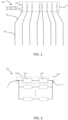
- FIG. 1 is a schematic structural diagram of a display device provided by one embodiment of the present application.
- the display device 100 provided by the embodiment of the present application includes a driving chip 10, a plurality of fan-out lines 20, and a plurality of data lines 30.
- the plurality of fan-out lines 20 are electrically connected to the driving chip 10.
- the plurality of data lines 30 are electrically connected to the plurality of fan-out lines 20 in a one-to-one correspondence, wherein the driving chip 10 includes a plurality of resistance modules 101, the plurality of resistance modules 101 are electrically connected to the plurality of fan-out lines 20 in a one-to-one correspondence, and the plurality of resistance modules 101 are configured to compensate different impedances of the fan-out lines 20.
- the display device 100 includes a display region and a non-display region, and the non-display region is provided with a circuit board connected with a driving chip.
- the plurality of fan-out lines 20 are provided between the driving chip 10 and the display region. Since the driving chip 10 is narrow and the display region is wider, it is necessary to connect the driving chip 10 with the corresponding data line 30 in the display region through the plurality of fan-out lines 20, which makes, the plurality of fan-out lines 20 corresponding to the same driver chip 10, and lengths of the fan-out lines 20 corresponding to different positions are different, so that each of fan-out lines 20 has a different impedance.
- a length of the fan-out line 20 positioned in a middle of the fan-out region is the shortest, while lengths of the fan-out lines 20 positioned on both sides of the fan-out region are gradually increases.
- a difference in length causes impedance difference between the fan-out lines 20, and the greater the length difference, the greater the impedance difference.
- the length difference between the fan-out lines 20 is very large, which results in the impedance difference of each fan-out lines 20 is also very large.
- a plurality of resistance modules 101 are provided in the driving chip 10 to compensate different impedances of the fan-out lines 20. That is, the plurality of resistance modules 101 compensate the impedance difference caused by the different lengths of the fan-out lines 20, so that an overall impedance tends to be equal, thereby improving the uneven charging of the display device 100 and improving the display effect of the display device 100.
- the driving chip 10 further includes a plurality of signal output modules 102.
- the plurality of signal output modules 102 are electrically connected to the plurality of resistance modules 101 in a one-to-one correspondence, and the signal output module 102 is configured to output driving signals to the corresponding resistance modules 101.
- FIG. 2 is a schematic diagram of a first structure of the resistance module in the display device provided by one embodiment of the present application.
- each of the resistance modules 101 includes a plurality of resistance units 101A arranged in parallel, and each of the resistance units 101A includes a compensation input terminal A, a compensation output terminal B, and a switch resistance pair 101B.
- the switch resistance pair 101B includes a compensation resistor and a compensation switch.
- the resistance unit 101A is configured to connect the compensation resistor between the compensation input terminal A and the compensation output terminal B.
- the switch resistance pair 101B includes a first compensation resistor 1011 and a first compensation switch 1012, and the first compensation resistor 1011 and the first compensation switch 1012 are connected in series between the compensation input terminal A and the compensation output terminal B.
- Each of the first compensation switches 1012 is a thin film transistor, wherein a control terminal of each of the thin film transistors are controlled by different compensation signals.
- a plurality of switch resistance pairs 101B are provided in the driving chip 10 to compensate the different impedances of the fan-out lines 20. That is, the plurality of resistance module 101 compensate the impedance difference caused by the different lengths of the fan-out lines 20, so that an overall impedance tends to be equal, thereby improving the uneven charging and the display effect of the display device 100.
- FIG. 3 is a schematic diagram of a second structure of the resistance module in the display device provided by one embodiment of the present application.
- each of the resistance modules 201 includes a plurality of resistance units 201A arranged in parallel, and each of the resistance units 201A includes a compensation input terminal A, a compensation output terminal B, and a switch resistance pair 201B.
- the switch resistance pair 201B includes a compensation resistor and a compensation switch, and the resistance unit 201A is configured to connect the compensation resistor between the compensation input terminal A and the compensation output terminal B.
- the switch resistance pair 201B includes at least two second compensation resistors 2011 and one second compensation switch 2012, the at least two second compensation resistors 2011 and the second compensation switch 2012 are connected in series between the compensation input terminal A and the compensation output terminal B, wherein the at least two second compensation resistors 2011 are connected in series.
- Each of the second compensation switch 2012 is a thin film transistor, wherein a control terminal of each of the thin film transistors are controlled by different compensation signals.
- a plurality of switch resistance pairs 201B are provided in the driving chip 10 to compensate the different impedances of the fan-out lines 20. That is, the plurality of switch resistance pairs 201B compensate the impedance difference caused by the different lengths of the fan-out lines 20, so that an overall impedance tends to be equal, thereby improving the uneven charging and the display effect of the display device 100.
- FIG. 4 is a schematic diagram of a third structure of the resistance module in the display device according to one embodiment of the present application.
- each of the resistance modules 301 includes a plurality of resistance units 301A arranged in parallel.
- Each of the resistance units 301A includes a compensation input terminal A, a compensation output terminal B, and a switch resistance pair 301B.
- the switch resistance pair 301B includes a compensation resistor and a compensation switch.
- the resistance unit 301A is configured to connect the compensation resistor between the compensation input terminal A and the compensation output terminal B.
- the switch resistance pair 301B includes at least two second compensation resistors 3011 and one second compensation switch 3012. At least two second compensation resistors 3011 and the second compensation switch 3012 are connected in series between the compensation input terminal A and the compensation output terminal B, wherein the at least two second compensation resistors 3011 are connected in parallel.
- Each of the second compensation switch 3012 is a thin film transistor, wherein a control terminal of each of the thin film transistors are controlled by different compensation signals.
- a plurality of switch resistance pairs 301B are provided in the driving chip 10 to compensate the different impedances of the fan-out lines 20. That is, the plurality of switch resistance pairs 301B compensate the impedance difference caused by the different lengths of the fan-out lines 20, so that an overall impedance tends to be equal, thereby improving the uneven charging and the display effect of the display device 100.
- FIG. 5 is a schematic diagram of a fourth structure of the resistance module in the display device according to one embodiment of the present application.
- each of the resistance modules 401 includes a plurality of resistance units 401A arranged in parallel, and each of the resistance units 401A includes a compensation input terminal A, a compensation output terminal B, and a switch resistance pair 401B.
- the switch resistance pair 401B includes a, compensation resistor and a compensation switch.
- the resistance unit 401A is configured to connect the compensation resistor between the compensation input terminal A and the compensation output terminal B.
- the switch resistance pair 401B includes at least two third compensation resistors 4011, at least two fourth compensation resistors 4012, and one third compensation switch 4013, and wherein the at least two third compensation resistors 4011, the at least two fourth compensation resistors 4012, and the third compensation switch 4013 are connected in series between the compensation input terminal A and the compensation output terminal B, wherein at least two third compensation resistors 4011 are connected in parallel, and at least two fourth compensation resistors 4012 are connected in parallel.
- Each of the third compensation switch 4013 is a thin film transistor, wherein a control terminal of each of the thin film transistors are controlled by different compensation signals.
- a plurality of switch resistance pairs 401B are provided in the driving chip 10 to compensate the different impedances of the fan-out lines 20. That is, the plurality of switch resistance pairs 401B compensate the impedance difference caused by the different lengths of the fan-out lines 20, so that an overall impedance tends to be equal, thereby improving the uneven charging and the display effect of the display device 100.
- FIG. 6 is a schematic diagram of a fifth structure of the resistance module in the display device according to one embodiment of the present application.
- each of the resistance module 501 includes a plurality of resistance units 501A arranged in parallel, and each of the resistance units 501A includes a compensation input terminal A, a compensation output terminal B, and a switch resistance pair 501B.
- the switch resistance pair 501B includes a compensation resistor and a compensation switch.
- the resistance unit 501A is configured to connect the compensation resistor between the compensation input terminal A and the compensation output terminal B.
- the switch resistance pair 501B includes a fifth compensation resistor 5011, at least two sixth compensation resistors 5012, and a fourth compensation switch 5013, wherein the fifth compensation resistor 5011, the at least two sixth compensation resistors 5012, and the fourth compensation switch 5013 are connected in series between the compensation input terminal A and the compensation output terminal B, and wherein at least two of the sixth compensation resistors 5012 are connected in parallel.
- Each of the fourth compensation switch 5013 is a thin film transistor, wherein a d control terminal of each of the thin film transistors are controlled by different compensation I signals.
- a plurality of switch resistance pairs are provided in the driving chip to compensate the different impedances of the fan-out lines. That is, the plurality of switch resistance pairs compensate the impedance difference caused by the different lengths of the fan-out lines, so that an overall impedance tends to be equal, thereby improving the uneven charging and the display effect of the display device.
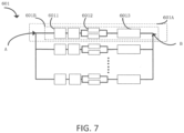
- FIG. 7 is a schematic diagram of a sixth structure of the resistance module in the display device provided by one embodiment of the present application.
- each of the resistance module 601 includes a plurality of resistance units 601A arranged in parallel, and each of the resistance units 601A includes a compensation input terminal A, a compensation output terminal B, and a switch resistance pair 601B.
- the switch resistance pair 601B includes a compensation resistor and a compensation switch.
- the resistance unit 601A is configured to connect the compensation resistor between the compensation input terminal A and the compensation output terminal B.
- the switch resistance pair 601B includes at least two seventh compensation resistors 6011, at least two eighth compensation resistors 6012, and one fifth compensation switch 6013, the at least two seventh compensation resistors 6011, the at least two eighth compensation resistors 6012, and the fifth compensation switch 6013 are connected in series between the compensation input terminal A and the compensation output terminal B. and wherein the at least two seventh compensation resistors 6011 are connected in series, and at least two eighth compensation resistors 6012 are connected in parallel.
- Each of the fifth compensation switch 6013 is a thin film transistor, wherein a control terminal of each of the thin film transistors are controlled by different compensation signals.
- a plurality of switch resistance pairs 601B are provided in the driving chip 10 to compensate the different impedances of the fan-out lines 20. That is, the plurality of switch resistance pairs 601B compensate the impedance difference caused by the different lengths of the fan-out lines 20, so that an overall impedance tends to be equal, thereby improving the uneven charging and the display effect of the display device 100.
Landscapes
- Engineering & Computer Science (AREA)
- Physics & Mathematics (AREA)
- Computer Hardware Design (AREA)
- General Physics & Mathematics (AREA)
- Theoretical Computer Science (AREA)
- Chemical & Material Sciences (AREA)
- Crystallography & Structural Chemistry (AREA)
- Control Of Indicators Other Than Cathode Ray Tubes (AREA)
- Devices For Indicating Variable Information By Combining Individual Elements (AREA)
- Control Of El Displays (AREA)
Abstract
Description
- The present application relates to a field of display technology, in particular to a display device.
- In a display device, a base substrate may include a display region and a non-display region, wherein the display region is provided with a plurality of data lines, and the non-display region is provided with a data driving chip and a plurality of fan-out lines connected to the plurality of data lines. Each of the fan-out lines provides display signals to the display region.
- However, a difference in the relative positions of the plurality of fan-out lines and the data driving chip causes each of fan-out lines has a different length, which will cause uneven impedances of fan-out lines, which in turn causes uneven charging of the display device, and affects a display effect of the display device.
- The present application provides a display device, which can improve an uneven charging of the display device, thereby improving the display effect of the display device
- In a first aspect, the present application provides a display device, includes
- a driving chip;
- a plurality of fan-out lines electrically connected to the driving chip; and
- a plurality of data lines electrically connected to the plurality of fan-out lines in a one-to-one correspondence;
- wherein the driving chip includes a plurality of resistance modules, the plurality of resistance modules are electrically connected to the plurality of fan-out lines in a one-to-one correspondence, and the plurality of resistance modules are configured to compensate different impedances of the fan-out lines;
- each of the resistance modules includes a plurality of resistance units arranged in parallel, and each of the resistance units comprises a compensation input terminal, a compensation output terminal, and a switch resistance pair, the switch resistance pair comprises a compensation resistor and a compensation switch, and the resistance unit is configured to connect the compensation resistor between the compensation input terminal and the compensation output terminal; and
- The driving chip further includes a plurality of signal output modules, the plurality of signal output modules are electrically connected to the plurality of resistance modules in a one-to-one correspondence, and the signal output module is configured to output driving signals to the corresponding resistance modules.
- in the display device provided by the present application, the switch resistance pair includes a first compensation resistor and a first compensation switch, and the first compensation resistor and the first compensation switch are connected in series between the compensation input terminal and the compensation output terminal.
- In the display device provided by the present application, the switch resistance pair includes at least two second compensation resistors and one second compensation switch, the at least two second compensation resistors and the second compensation switch are connected in series between the compensation input terminal and the compensation output terminal.
- in the display device provided by the present application, at least two of the second compensation resistors are connected in series, or at least two of the second compensation resistors are connected in parallel.
- In the display device provided by the present application, the switch resistance pair includes at least two third compensation resistors, at least two fourth compensation resistors, and one third compensation switch, and wherein the at least two third compensation resistors, the at least two fourth compensation resistors, and the third compensation switch are connected in series between the compensation input terminal and the compensation output terminal; and wherein the at least two third compensation resistors are connected in parallel, the at least two fourth compensation resistors are connected in parallel.
- In the display device provided by the present application, the switch resistance pair includes a fifth compensation resistor, at least two sixth compensation resistors, and a fourth compensation switch, wherein the fifth compensation resistor, the at least two sixth compensation resistors, and the fourth compensation switch are connected in series between the compensation input terminal and the compensation output terminal, and wherein at least two of the sixth compensation resistors are connected in parallel.
- In the display device provided by the present application, the switch resistance pair includes at least two seventh compensation resistors, at least two eighth compensation resistors, and one fifth compensation switch, the at least two seventh compensation resistors, the at least two eighth compensation resistors, and the fifth compensation switch are connected in series between the compensation input terminal and the compensation output terminal; and wherein the at least two seventh compensation resistors are connected in series, and the at least two eighth compensation resistors are connected in parallel.
- In the display device provided by the present application, each of the compensation switches is a thin film transistor, and wherein a control terminal of each of the thin film transistors are controlled by different compensation signals
- In a second aspect, the present application provides a display device, including:
- a driving chip;
- a plurality of fan-out lines electrically connected to the driving chip; and
- a plurality of data lines electrically connected to the plurality of fan-out lines in a one-to-one correspondence;
- wherein the driving chip includes a plurality of resistance modules, the plurality of resistance modules are electrically connected to the plurality of fan-out lines in a one-to-one correspondence, and the plurality of resistance modules are configured to compensate different impedances of the fan-out lines.
- In the display device provided by the present application, each of the resistance modules includes a plurality of resistance units arranged in parallel, and each of the resistance units includes a compensation input terminal, a compensation output terminal, and a switch resistance pair, the switch resistance pair includes a compensation resistor and a compensation switch, and the resistance unit is configured to connect the compensation resistor between the compensation input terminal and the compensation output terminal.
- In the display device provided by the present application, the switch resistance pair includes a first compensation resistor and a first compensation switch, and the first compensation resistor and the first compensation switch are connected in series between the compensation input terminal and the compensation output terminal.
- In the display device provided by the present application, the switch resistance pair includes at least two second compensation resistors and one second compensation switch, the at least two second compensation resistors and the second compensation switch are connected in series between the compensation input terminal and the compensation output terminal.
- In the display device provided by the present application, at least two of the second compensation resistors are connected in series, or at least two of the second compensation resistors are connected in parallel.
- In the display device provided by the present application, the switch resistance pair includes at least two third compensation resistors, at least two fourth compensation resistors, and one third compensation switch, and wherein the at least two third compensation resistors, the at least two fourth compensation resistors, and the third compensation switch are connected in series between the compensation input terminal and the compensation output terminal; and wherein the at least two third, compensation resistors are connected in parallel, the at least two fourth compensation resistors are connected in parallel.
- In the display device provided by the present application, the switch resistance pair includes a fifth compensation resistor, at least two sixth compensation resistors, and a fourth compensation switch, wherein the fifth compensation resistor, the at least two sixth compensation resistors, and the fourth compensation switch are connected in series between the compensation input terminal and the compensation output terminal, and wherein at least two of the sixth compensation resistors are connected in parallel.
- In the display device provided by the present application, the switch resistance pair includes at least two seventh compensation resistors, at least two eighth compensation resistors, and one fifth compensation switch, the least two seventh compensation resistors, the at least two eighth compensation resistors, and the fifth compensation switch are connected in series between the compensation input terminal and the compensation output terminal; and wherein the at least two seventh compensation resistors are connected in series, and the at least two eighth compensation resistors are connected in parallel.
- In the display device provided by the present application, each of the compensation switches is a thin film transistor, and wherein a control terminal of each of the thin film transistors are controlled by different compensation signals.
- In the display device provided by the present application, the driving chip further includes a plurality of signal output modules, the plurality of signal output modules are electrically connected to the plurality of resistance modules in a one-to-one correspondence, and the signal output module is configured to output driving signals to the corresponding resistance modules.
- In the display device provided by the present application, a plurality of resistance modules are provided in the driving chip to compensate the different impedances of the fan-out lines. That is, the resistance module compensates the impedance difference caused by the different length of the fan-out lines, so that an overall impedances tend to be equal, thereby improving an uneven charging of the display device and improving the display effect of the display device.
- In order to explain the technical solutions in the embodiments of the present application more clearly, the following will briefly introduce the figures needed in the description of the embodiments. Obviously, the figures in the following description are only some embodiments of the present application. For those skilled in the art, without inventive steps, other figures can be obtained based on these figures.
-
FIG. 1 is a schematic structural diagram of a display device provided by one embodiment of the present application. -
FIG. 2 is a schematic diagram of a first structure of a resistance module in the display device provided by one embodiment of the present application. -
FIG. 3 is a schematic diagram of a second structure of the resistance module in the display device provided by one embodiment of the present application. -
FIG. 4 is a schematic diagram of a third structure of the resistance module in the display device provided by one embodiment of the present application: -
FIG. 5 is a schematic diagram of a fourth structure of the resistance module in the display device provided by one embodiment of the present application. -
FIG. 6 is a schematic diagram of a fifth structure of the resistance module in the display device provided by one embodiment of the present application. -
FIG. 7 is a schematic diagram of a sixth structure of the resistance module in the display device provided by one embodiment of the present application. - The technical solutions in the embodiments of the present application will be clearly and completely described below in conjunction with the figures in the embodiments of the present application. Obviously, the described embodiments are only a part of the embodiments of the present application, rather than all the embodiments. Based on the embodiments in the present application, all other embodiments obtained by those skilled in the art without inventive steps shall fall within a protection scope of the present application.
- It should be understood that the specific embodiments described here are only used to illustrate and explain the present application, and are not used to limit the present application. The claims of the present application and the terms: first, second, third, fourth, fifth, sixth, seventh, and eighth. etc. in the specification are used to distinguish different objects, not to describe a specific order.
- Please refer to
FIG. 1. FIG. 1 is a schematic structural diagram of a display device provided by one embodiment of the present application. As shown inFIG. 1 , thedisplay device 100 provided by the embodiment of the present application includes adriving chip 10, a plurality of fan-outlines 20, and a plurality ofdata lines 30. The plurality of fan-outlines 20 are electrically connected to thedriving chip 10. The plurality ofdata lines 30 are electrically connected to the plurality of fan-outlines 20 in a one-to-one correspondence, wherein the drivingchip 10 includes a plurality ofresistance modules 101, the plurality ofresistance modules 101 are electrically connected to the plurality of fan-outlines 20 in a one-to-one correspondence, and the plurality ofresistance modules 101 are configured to compensate different impedances of the fan-outlines 20. - It should be noted that the
display device 100 includes a display region and a non-display region, and the non-display region is provided with a circuit board connected with a driving chip. The plurality of fan-outlines 20 are provided between thedriving chip 10 and the display region. Since thedriving chip 10 is narrow and the display region is wider, it is necessary to connect thedriving chip 10 with thecorresponding data line 30 in the display region through the plurality of fan-outlines 20, which makes, the plurality of fan-outlines 20 corresponding to thesame driver chip 10, and lengths of the fan-outlines 20 corresponding to different positions are different, so that each of fan-outlines 20 has a different impedance. - Generally, a length of the fan-out
line 20 positioned in a middle of the fan-out region is the shortest, while lengths of the fan-outlines 20 positioned on both sides of the fan-out region are gradually increases. A difference in length causes impedance difference between the fan-outlines 20, and the greater the length difference, the greater the impedance difference. Especially for adisplay device 100 designed with a high-pin-count driver chip 10, corresponding to thesame driver chip 10 and one fan-out region, the length difference between the fan-outlines 20 is very large, which results in the impedance difference of each fan-outlines 20 is also very large. - In the
display device 100 provided by the present application, a plurality ofresistance modules 101 are provided in thedriving chip 10 to compensate different impedances of the fan-outlines 20. That is, the plurality ofresistance modules 101 compensate the impedance difference caused by the different lengths of the fan-outlines 20, so that an overall impedance tends to be equal, thereby improving the uneven charging of thedisplay device 100 and improving the display effect of thedisplay device 100. - The
driving chip 10 further includes a plurality ofsignal output modules 102. The plurality ofsignal output modules 102 are electrically connected to the plurality ofresistance modules 101 in a one-to-one correspondence, and thesignal output module 102 is configured to output driving signals to thecorresponding resistance modules 101. - Please refer to
FIG. 2. FIG. 2 is a schematic diagram of a first structure of the resistance module in the display device provided by one embodiment of the present application. As shown inFIG. 1 and FIG. 2 , each of theresistance modules 101 includes a plurality ofresistance units 101A arranged in parallel, and each of theresistance units 101A includes a compensation input terminal A, a compensation output terminal B, and aswitch resistance pair 101B. Theswitch resistance pair 101B includes a compensation resistor and a compensation switch. Theresistance unit 101A is configured to connect the compensation resistor between the compensation input terminal A and the compensation output terminal B. - The
switch resistance pair 101B includes afirst compensation resistor 1011 and afirst compensation switch 1012, and thefirst compensation resistor 1011 and thefirst compensation switch 1012 are connected in series between the compensation input terminal A and the compensation output terminal B. - Each of the
first compensation switches 1012 is a thin film transistor, wherein a control terminal of each of the thin film transistors are controlled by different compensation signals. - In the
display device 100 provided in the present application, a plurality of switch resistance pairs 101B are provided in thedriving chip 10 to compensate the different impedances of the fan-outlines 20. That is, the plurality ofresistance module 101 compensate the impedance difference caused by the different lengths of the fan-outlines 20, so that an overall impedance tends to be equal, thereby improving the uneven charging and the display effect of thedisplay device 100. - Please refer to
FIG. 3, FIG. 3 is a schematic diagram of a second structure of the resistance module in the display device provided by one embodiment of the present application. As shown inFIGs. 1 and3 , each of theresistance modules 201 includes a plurality ofresistance units 201A arranged in parallel, and each of theresistance units 201A includes a compensation input terminal A, a compensation output terminal B, and aswitch resistance pair 201B. Theswitch resistance pair 201B includes a compensation resistor and a compensation switch, and theresistance unit 201A is configured to connect the compensation resistor between the compensation input terminal A and the compensation output terminal B. - The
switch resistance pair 201B includes at least twosecond compensation resistors 2011 and onesecond compensation switch 2012, the at least twosecond compensation resistors 2011 and thesecond compensation switch 2012 are connected in series between the compensation input terminal A and the compensation output terminal B, wherein the at least twosecond compensation resistors 2011 are connected in series. - Each of the
second compensation switch 2012 is a thin film transistor, wherein a control terminal of each of the thin film transistors are controlled by different compensation signals. - In the
display device 100 provided in the present application, a plurality of switch resistance pairs 201B are provided in thedriving chip 10 to compensate the different impedances of the fan-outlines 20. That is, the plurality of switch resistance pairs 201B compensate the impedance difference caused by the different lengths of the fan-outlines 20, so that an overall impedance tends to be equal, thereby improving the uneven charging and the display effect of thedisplay device 100. - Please refer to
FIG. 4. FIG. 4 is a schematic diagram of a third structure of the resistance module in the display device according to one embodiment of the present application. As shown inFIGs. 1 and4 , each of theresistance modules 301 includes a plurality ofresistance units 301A arranged in parallel. Each of theresistance units 301A includes a compensation input terminal A, a compensation output terminal B, and aswitch resistance pair 301B. Theswitch resistance pair 301B includes a compensation resistor and a compensation switch. Theresistance unit 301A is configured to connect the compensation resistor between the compensation input terminal A and the compensation output terminal B. - The
switch resistance pair 301B includes at least twosecond compensation resistors 3011 and onesecond compensation switch 3012. At least twosecond compensation resistors 3011 and thesecond compensation switch 3012 are connected in series between the compensation input terminal A and the compensation output terminal B, wherein the at least twosecond compensation resistors 3011 are connected in parallel. - Each of the
second compensation switch 3012 is a thin film transistor, wherein a control terminal of each of the thin film transistors are controlled by different compensation signals. - In the
display device 100 provided in the present application, a plurality of switch resistance pairs 301B are provided in thedriving chip 10 to compensate the different impedances of the fan-outlines 20. That is, the plurality of switch resistance pairs 301B compensate the impedance difference caused by the different lengths of the fan-outlines 20, so that an overall impedance tends to be equal, thereby improving the uneven charging and the display effect of thedisplay device 100. - Please refer to
FIG. 5. FIG. 5 is a schematic diagram of a fourth structure of the resistance module in the display device according to one embodiment of the present application. As shown inFIGs. 1 and5 , each of theresistance modules 401 includes a plurality ofresistance units 401A arranged in parallel, and each of theresistance units 401A includes a compensation input terminal A, a compensation output terminal B, and aswitch resistance pair 401B. Theswitch resistance pair 401B includes a, compensation resistor and a compensation switch. Theresistance unit 401A is configured to connect the compensation resistor between the compensation input terminal A and the compensation output terminal B. - The
switch resistance pair 401B includes at least twothird compensation resistors 4011, at least twofourth compensation resistors 4012, and onethird compensation switch 4013, and wherein the at least twothird compensation resistors 4011, the at least twofourth compensation resistors 4012, and thethird compensation switch 4013 are connected in series between the compensation input terminal A and the compensation output terminal B, wherein at least twothird compensation resistors 4011 are connected in parallel, and at least twofourth compensation resistors 4012 are connected in parallel. - Each of the
third compensation switch 4013 is a thin film transistor, wherein a control terminal of each of the thin film transistors are controlled by different compensation signals. - In the
display device 100 provided in the present application, a plurality of switch resistance pairs 401B are provided in thedriving chip 10 to compensate the different impedances of the fan-outlines 20. That is, the plurality of switch resistance pairs 401B compensate the impedance difference caused by the different lengths of the fan-outlines 20, so that an overall impedance tends to be equal, thereby improving the uneven charging and the display effect of thedisplay device 100. - Please refer to
FIG. 6. FIG. 6 is a schematic diagram of a fifth structure of the resistance module in the display device according to one embodiment of the present application. As shown inFIG. 1 andFIG. 6 , each of theresistance module 501 includes a plurality of resistance units 501A arranged in parallel, and each of the resistance units 501A includes a compensation input terminal A, a compensation output terminal B, and aswitch resistance pair 501B. Theswitch resistance pair 501B includes a compensation resistor and a compensation switch. The resistance unit 501A is configured to connect the compensation resistor between the compensation input terminal A and the compensation output terminal B. - The
switch resistance pair 501B includes afifth compensation resistor 5011, at least twosixth compensation resistors 5012, and afourth compensation switch 5013, wherein thefifth compensation resistor 5011, the at least twosixth compensation resistors 5012, and thefourth compensation switch 5013 are connected in series between the compensation input terminal A and the compensation output terminal B, and wherein at least two of thesixth compensation resistors 5012 are connected in parallel. - Each of the
fourth compensation switch 5013 is a thin film transistor, wherein a d control terminal of each of the thin film transistors are controlled by different compensation I signals. - in the display device provided by the present application, a plurality of switch resistance pairs are provided in the driving chip to compensate the different impedances of the fan-out lines. That is, the plurality of switch resistance pairs compensate the impedance difference caused by the different lengths of the fan-out lines, so that an overall impedance tends to be equal, thereby improving the uneven charging and the display effect of the display device.
- Please refer to
FIG. 7. FIG. 7 is a schematic diagram of a sixth structure of the resistance module in the display device provided by one embodiment of the present application. As shown inFIG. 1 andFIG. 7 , each of theresistance module 601 includes a plurality ofresistance units 601A arranged in parallel, and each of theresistance units 601A includes a compensation input terminal A, a compensation output terminal B, and aswitch resistance pair 601B. Theswitch resistance pair 601B includes a compensation resistor and a compensation switch. Theresistance unit 601A is configured to connect the compensation resistor between the compensation input terminal A and the compensation output terminal B. - The
switch resistance pair 601B includes at least twoseventh compensation resistors 6011, at least twoeighth compensation resistors 6012, and onefifth compensation switch 6013, the at least twoseventh compensation resistors 6011, the at least twoeighth compensation resistors 6012, and thefifth compensation switch 6013 are connected in series between the compensation input terminal A and the compensation output terminal B. and wherein the at least twoseventh compensation resistors 6011 are connected in series, and at least twoeighth compensation resistors 6012 are connected in parallel. - Each of the
fifth compensation switch 6013 is a thin film transistor, wherein a control terminal of each of the thin film transistors are controlled by different compensation signals. - In the
display device 100 provided in the present application, a plurality of switch resistance pairs 601B are provided in thedriving chip 10 to compensate the different impedances of the fan-outlines 20. That is, the plurality of switch resistance pairs 601B compensate the impedance difference caused by the different lengths of the fan-outlines 20, so that an overall impedance tends to be equal, thereby improving the uneven charging and the display effect of thedisplay device 100. - The above is a detailed introduction to the display provided by the embodiments of the present application. Specific embodiments are used in the specification to illustrate the principles and implementation of the present application. The descriptions of the above embodiments are only used to help understand the methods and core ideas of the present application. At the same time, for those skilled in the art, according to the idea of the present application, there will be changes in the specific implementation and the scope of application. In summary, the content of this specification should not be construed as a limitation to the present application.
Claims (18)
- A display device, comprising:a driving chip;a plurality of fan-out lines electrically connected to the driving chip; anda plurality of data lines electrically connected to the plurality of fan-out lines in a one-to-one correspondence;wherein the driving chip comprises a plurality of resistance modules, the plurality of resistance modules are electrically connected to the plurality of fan-out lines in a one-to-one correspondence, and the plurality of resistance modules are configured to compensate different impedances of the fan-out lines;each of the resistance modules comprises a plurality of resistance units arranged in parallel, and each of the resistance units comprises a compensation input terminal, a compensation output terminal, and a switch resistance pair, the switch resistance pair comprises a compensation resistor and a compensation switch, and the resistance unit is configured to connect the compensation resistor between the compensation input terminal and the compensation output terminal; andthe driving chip further comprises a plurality of signal output modules, the plurality of signal output modules are electrically connected to the plurality of resistance modules in a one-to-one correspondence, and the signal output module is configured to output driving signals to the corresponding resistance modules.
- The display device according to claim 1, wherein the switch resistance pair comprises a first compensation resistor and a first compensation switch, and the first compensation resistor and the first compensation switch are connected in series between the compensation input terminal and the compensation output terminal.
- The display device according to claim 1, wherein the switch resistance pair comprises at least two second compensation resistors and one second compensation switch, the at least two second compensation resistors and the second compensation switch are connected in series between the compensation input terminal and the compensation output terminal.
- The display device according to claim 3, wherein at least two of the second compensation resistors are connected in series, or at least two of the second compensation resistors are connected in parallel.
- The display device according to claim 1, wherein the switch resistance pair comprises at least two third compensation resistors, at least two fourth compensation resistors, and one third compensation switch, and wherein the at least two third compensation resistors, the at least two fourth compensation resistors, and the third compensation switch are connected in series between the compensation input terminal and the compensation output terminal; and
wherein the at least two third compensation resistors are connected in parallel, the at least two fourth compensation resistors are connected in parallel. - The display device according to claim 1, wherein the switch resistance pair comprises a fifth compensation resistor, at least two sixth compensation resistors, and a fourth compensation switch, wherein the fifth compensation resistor, the at least two sixth compensation resistors, and the fourth compensation switch are connected in series between the compensation input terminal and the compensation output terminal, and wherein at least two of the sixth compensation resistors are connected in parallel.
- The display device according to claim 1, wherein the switch resistance pair comprises at least two seventh compensation resistors, at least two eighth compensation resistors, and one fifth compensation switch, the at least two seventh compensation resistors, the at least two eighth compensation resistors, and the fifth compensation switch are connected in series between the compensation input terminal and the compensation output terminal; and
wherein the at least two seventh compensation resistors are connected in series, and the at least two eighth compensation resistors are connected in parallel. - The display device according to claim 1, wherein each of the compensation switches is a thin film transistor, and wherein a control terminal of each of the thin film transistors are controlled by different compensation signals.
- A display device, comprisinga driving chip;a plurality of fan-out lines electrically connected to the driving chip; anda plurality of data lines electrically connected to the plurality of fan-out lines in a one-to-one correspondence;wherein the driving chip comprises a plurality of resistance modules, the plurality of resistance modules are electrically connected to the plurality of fan-out lines in a one-to-one correspondence, and the plurality of resistance modules are configured to compensate different impedances of the fan-out lines.
- The display device according to claim 9, wherein each of the resistance modules comprises a plurality of resistance units arranged in parallel, and each of the resistance units comprises a compensation input terminal, a compensation output terminal, and a switch resistance pair, the switch resistance pair comprises a compensation resistor and a compensation switch, and the resistance unit is configured to connect the compensation resistor between the compensation input terminal and the compensation output terminal.
- The display device according to claim 10, wherein the switch resistance pair comprises a first compensation resistor and a first compensation switch, and the first compensation resistor and the first compensation switch are connected in series between the compensation input terminal and the compensation output terminal.
- The display device according to claim 10, wherein the switch resistance pair comprises at least two second compensation resistors and one second compensation switch, the at least two second compensation resistors and the second compensation switch are connected in series between the compensation input terminal and the compensation output terminal.
- The display device according to claim 12, wherein at least two of the second compensation resistors are connected in series, or at least two of the second compensation resistors are connected in parallel.
- The display device according to claim 10, wherein the switch resistance pair comprises at least two third compensation resistors, at least two fourth compensation resistors, and one third compensation switch, and wherein the at least two third compensation resistors, the at least two fourth compensation resistors, and the third compensation switch are connected in series between the compensation input terminal and the compensation output terminal; and
wherein the at least two third compensation resistors are connected in parallel, the at least two fourth compensation resistors are connected in parallel. - The display device according to claim 10, wherein the switch resistance pair comprises a fifth compensation resistor, at least two sixth compensation resistors, and a fourth compensation switch, wherein the fifth compensation resistor, the at least two sixth compensation resistors, and the fourth compensation switch are connected in series between the compensation input terminal and the compensation output terminal, and wherein at least two of the sixth compensation resistors are connected inparallel.
- The display device according to claim 10, wherein the switch resistance pair comprises at least two seventh compensation resistors, at least two eighth compensation resistors, and one fifth compensation switch, the least two seventh compensation resistors, the at least two eighth compensation resistors, and the fifth compensation switch are connected in series between the compensation input terminal and the compensation output terminal; and
wherein the at least two seventh compensation resistors are connected in series, and the at least two eighth compensation resistors are connected in parallel. - The display device according to claim 10, wherein each of the compensation switches is a thin film transistor, and wherein a control terminal of each of the thin film transistors are controlled by different compensation signals.
- The display device according to claim 9, wherein the driving chip further comprises a plurality of signal output modules, the plurality of signal output modules are electrically connected to the plurality of resistance modules in a one-to-one correspondence, and the signal output module is configured to output driving signals to the corresponding resistance modules.
Applications Claiming Priority (2)
| Application Number | Priority Date | Filing Date | Title |
|---|---|---|---|
| CN202110953214.0A CN113690255B (en) | 2021-08-19 | 2021-08-19 | display device |
| PCT/CN2021/114634 WO2023019620A1 (en) | 2021-08-19 | 2021-08-26 | Display device |
Publications (2)
| Publication Number | Publication Date |
|---|---|
| EP4391060A1 true EP4391060A1 (en) | 2024-06-26 |
| EP4391060A4 EP4391060A4 (en) | 2025-05-28 |
Family
ID=85228569
Family Applications (1)
| Application Number | Title | Priority Date | Filing Date |
|---|---|---|---|
| EP21815093.6A Pending EP4391060A4 (en) | 2021-08-19 | 2021-08-26 | DISPLAY DEVICE |
Country Status (4)
| Country | Link |
|---|---|
| US (1) | US11763714B2 (en) |
| EP (1) | EP4391060A4 (en) |
| JP (1) | JP7451559B2 (en) |
| KR (1) | KR102586850B1 (en) |
Family Cites Families (25)
| Publication number | Priority date | Publication date | Assignee | Title |
|---|---|---|---|---|
| KR100812073B1 (en) * | 2006-11-09 | 2008-03-07 | 삼성에스디아이 주식회사 | Differential signal transmission system and flat panel display device having same |
| KR101287042B1 (en) * | 2006-12-01 | 2013-07-17 | 삼성디스플레이 주식회사 | Display panel and display device having the same |
| KR20080053781A (en) | 2006-12-11 | 2008-06-16 | 삼성전자주식회사 | Fanout wiring structure and flat panel and flat panel display device |
| JP2009230108A (en) * | 2008-02-29 | 2009-10-08 | Canon Inc | Drive circuit of display panel and display apparatus |
| US8446406B2 (en) * | 2009-07-03 | 2013-05-21 | Lg Display Co., Ltd. | Liquid crystal display |
| JP5778485B2 (en) * | 2011-06-03 | 2015-09-16 | ルネサスエレクトロニクス株式会社 | Panel display data driver |
| KR102048437B1 (en) * | 2013-08-30 | 2019-11-25 | 엘지디스플레이 주식회사 | Thin film transistor substrate and Display Device using the same |
| KR102196101B1 (en) * | 2014-10-23 | 2020-12-30 | 삼성디스플레이 주식회사 | Display apparatus |
| CN104809997B (en) * | 2015-05-07 | 2018-02-23 | 武汉华星光电技术有限公司 | A kind of control circuit and display device |
| JP2017021087A (en) * | 2015-07-07 | 2017-01-26 | パナソニック液晶ディスプレイ株式会社 | Drive circuit and display |
| US10410599B2 (en) * | 2015-08-13 | 2019-09-10 | Samsung Electronics Co., Ltd. | Source driver integrated circuit for ompensating for display fan-out and display system including the same |
| CN105204248A (en) | 2015-10-10 | 2015-12-30 | 重庆京东方光电科技有限公司 | Array substrate and display device |
| KR102445957B1 (en) * | 2016-04-29 | 2022-09-22 | 엘지디스플레이 주식회사 | Driver ic, controller, and display device |
| KR102504613B1 (en) * | 2016-05-25 | 2023-03-02 | 삼성디스플레이 주식회사 | Display apparatus and method of driving the same |
| CN106990869B (en) * | 2017-04-07 | 2019-09-24 | 上海天马微电子有限公司 | Touch display panel and touch display device |
| US10902816B2 (en) * | 2017-04-10 | 2021-01-26 | Novatek Microelectronics Corp. | Integrated circuit for driving display panel and fan-out compensation method thereof |
| CN107248388B (en) * | 2017-07-03 | 2019-07-16 | 京东方科技集团股份有限公司 | Driving device, driving method and display device |
| CN208737865U (en) | 2018-09-21 | 2019-04-12 | 惠科股份有限公司 | impedance difference compensation circuit, display panel and mobile terminal |
| US20200098320A1 (en) * | 2018-09-21 | 2020-03-26 | HKC Corporation Limited | Impedance difference compensation circuit, display panel and mobile terminal |
| CN109166515B (en) * | 2018-10-29 | 2019-09-17 | 惠科股份有限公司 | display device and adjusting method thereof |
| CN109976052A (en) | 2019-04-29 | 2019-07-05 | 深圳市华星光电技术有限公司 | Display device |
| CN210323694U (en) * | 2019-06-11 | 2020-04-14 | 重庆惠科金渝光电科技有限公司 | Display panel's drive module and display device |
| CN210325151U (en) | 2019-06-11 | 2020-04-14 | 重庆惠科金渝光电科技有限公司 | Display panel's drive module and display device |
| CN111028797B (en) * | 2019-12-04 | 2021-01-15 | 深圳市华星光电半导体显示技术有限公司 | Display driving circuit and liquid crystal display panel |
| CN112201165B (en) | 2020-10-23 | 2021-12-28 | Tcl华星光电技术有限公司 | Display device and electronic apparatus |
-
2021
- 2021-08-26 JP JP2021560074A patent/JP7451559B2/en active Active
- 2021-08-26 US US17/600,067 patent/US11763714B2/en active Active
- 2021-08-26 EP EP21815093.6A patent/EP4391060A4/en active Pending
- 2021-08-26 KR KR1020217036336A patent/KR102586850B1/en active Active
Also Published As
| Publication number | Publication date |
|---|---|
| KR20230028105A (en) | 2023-02-28 |
| US11763714B2 (en) | 2023-09-19 |
| JP7451559B2 (en) | 2024-03-18 |
| US20230059909A1 (en) | 2023-02-23 |
| KR102586850B1 (en) | 2023-10-11 |
| JP2023541727A (en) | 2023-10-04 |
| EP4391060A4 (en) | 2025-05-28 |
Similar Documents
| Publication | Publication Date | Title |
|---|---|---|
| US5553250A (en) | Bus terminating circuit | |
| CN206848661U (en) | Array base palte and display device | |
| JP2019518238A (en) | Overcurrent protection circuit of display panel and array substrate row drive circuit thereof | |
| US20190385547A1 (en) | Control circuit of display panel, display device and control method thereof | |
| US7705953B2 (en) | Display device wherein a termination resistor is formed on a second connecting substrate | |
| US20220404405A1 (en) | Display device and detection method for impedance of display device | |
| CN107608150A (en) | display device and repairing method thereof | |
| CN113690255B (en) | display device | |
| WO2021203493A1 (en) | Display apparatus and electronic device | |
| US7573353B2 (en) | Circuit topology for multiple loads | |
| CN111261089B (en) | Display device and electronic apparatus | |
| CN101539696B (en) | Circuit and method for regulating display difference | |
| US11763714B2 (en) | Display device having driving chip | |
| US7746195B2 (en) | Circuit topology for multiple loads | |
| US8085008B2 (en) | System for accounting for switch impendances | |
| US20240046849A1 (en) | Data signal regulating circuit and display device | |
| CN210091692U (en) | Display panel and device | |
| CN110047422B (en) | Display panel, display device and driving method of display panel | |
| US12190766B2 (en) | Driving circuit and display device | |
| US20190079362A1 (en) | Display panel and repair method thereof | |
| CN1249827A (en) | Electric circuit and method for eliminating influence of voltage drop | |
| CN206471102U (en) | A kind of test device and display panel | |
| US11545098B2 (en) | Driving apparatus for display panel having selection circuit for outputting a plurality of driving voltages | |
| JPH01129175A (en) | Interface circuit | |
| EA049167B1 (en) | DISPLAY DEVICE |
Legal Events
| Date | Code | Title | Description |
|---|---|---|---|
| STAA | Information on the status of an ep patent application or granted ep patent |
Free format text: STATUS: UNKNOWN |
|
| STAA | Information on the status of an ep patent application or granted ep patent |
Free format text: STATUS: THE INTERNATIONAL PUBLICATION HAS BEEN MADE |
|
| PUAI | Public reference made under article 153(3) epc to a published international application that has entered the european phase |
Free format text: ORIGINAL CODE: 0009012 |
|
| STAA | Information on the status of an ep patent application or granted ep patent |
Free format text: STATUS: REQUEST FOR EXAMINATION WAS MADE |
|
| 17P | Request for examination filed |
Effective date: 20211207 |
|
| AK | Designated contracting states |
Kind code of ref document: A1 Designated state(s): AL AT BE BG CH CY CZ DE DK EE ES FI FR GB GR HR HU IE IS IT LI LT LU LV MC MK MT NL NO PL PT RO RS SE SI SK SM TR |
|
| DAV | Request for validation of the european patent (deleted) | ||
| DAX | Request for extension of the european patent (deleted) | ||
| REG | Reference to a national code |
Ref country code: DE Ref legal event code: R079 Free format text: PREVIOUS MAIN CLASS: H01L0027120000 Ipc: G09G0003327500 |
|
| A4 | Supplementary search report drawn up and despatched |
Effective date: 20250429 |
|
| RIC1 | Information provided on ipc code assigned before grant |
Ipc: G09G 3/36 20060101ALN20250423BHEP Ipc: G09G 3/3275 20160101AFI20250423BHEP |
|
| STAA | Information on the status of an ep patent application or granted ep patent |
Free format text: STATUS: EXAMINATION IS IN PROGRESS |
|
| 17Q | First examination report despatched |
Effective date: 20251217 |