EP4390936A1 - Material stack for microelectronic device, a microelectronic device that integrates such stack and method for manufacturing such stack - Google Patents
Material stack for microelectronic device, a microelectronic device that integrates such stack and method for manufacturing such stack Download PDFInfo
- Publication number
- EP4390936A1 EP4390936A1 EP23219178.3A EP23219178A EP4390936A1 EP 4390936 A1 EP4390936 A1 EP 4390936A1 EP 23219178 A EP23219178 A EP 23219178A EP 4390936 A1 EP4390936 A1 EP 4390936A1
- Authority
- EP
- European Patent Office
- Prior art keywords
- layer
- crystalline
- doped
- undoped
- chalcogenide
- Prior art date
- Legal status (The legal status is an assumption and is not a legal conclusion. Google has not performed a legal analysis and makes no representation as to the accuracy of the status listed.)
- Granted
Links
Images




Classifications
-
- H—ELECTRICITY
- H10—SEMICONDUCTOR DEVICES; ELECTRIC SOLID-STATE DEVICES NOT OTHERWISE PROVIDED FOR
- H10N—ELECTRIC SOLID-STATE DEVICES NOT OTHERWISE PROVIDED FOR
- H10N70/00—Solid-state devices having no potential barriers, and specially adapted for rectifying, amplifying, oscillating or switching
- H10N70/011—Manufacture or treatment of multistable switching devices
- H10N70/021—Formation of switching materials, e.g. deposition of layers
- H10N70/026—Formation of switching materials, e.g. deposition of layers by physical vapor deposition, e.g. sputtering
-
- H—ELECTRICITY
- H10—SEMICONDUCTOR DEVICES; ELECTRIC SOLID-STATE DEVICES NOT OTHERWISE PROVIDED FOR
- H10N—ELECTRIC SOLID-STATE DEVICES NOT OTHERWISE PROVIDED FOR
- H10N70/00—Solid-state devices having no potential barriers, and specially adapted for rectifying, amplifying, oscillating or switching
- H10N70/801—Constructional details of multistable switching devices
- H10N70/881—Switching materials
- H10N70/882—Compounds of sulfur, selenium or tellurium, e.g. chalcogenides
- H10N70/8828—Tellurides, e.g. GeSbTe
-
- G—PHYSICS
- G11—INFORMATION STORAGE
- G11C—STATIC STORES
- G11C13/00—Digital stores characterised by the use of storage elements not covered by groups G11C11/00, G11C23/00, or G11C25/00
- G11C13/0002—Digital stores characterised by the use of storage elements not covered by groups G11C11/00, G11C23/00, or G11C25/00 using resistive RAM [RRAM] elements
- G11C13/0004—Digital stores characterised by the use of storage elements not covered by groups G11C11/00, G11C23/00, or G11C25/00 using resistive RAM [RRAM] elements comprising amorphous/crystalline phase transition cells
-
- H—ELECTRICITY
- H10—SEMICONDUCTOR DEVICES; ELECTRIC SOLID-STATE DEVICES NOT OTHERWISE PROVIDED FOR
- H10B—ELECTRONIC MEMORY DEVICES
- H10B63/00—Resistance change memory devices, e.g. resistive RAM [ReRAM] devices
- H10B63/10—Phase change RAM [PCRAM, PRAM] devices
-
- H—ELECTRICITY
- H10—SEMICONDUCTOR DEVICES; ELECTRIC SOLID-STATE DEVICES NOT OTHERWISE PROVIDED FOR
- H10N—ELECTRIC SOLID-STATE DEVICES NOT OTHERWISE PROVIDED FOR
- H10N70/00—Solid-state devices having no potential barriers, and specially adapted for rectifying, amplifying, oscillating or switching
- H10N70/011—Manufacture or treatment of multistable switching devices
- H10N70/041—Modification of switching materials after formation, e.g. doping
-
- H—ELECTRICITY
- H10—SEMICONDUCTOR DEVICES; ELECTRIC SOLID-STATE DEVICES NOT OTHERWISE PROVIDED FOR
- H10N—ELECTRIC SOLID-STATE DEVICES NOT OTHERWISE PROVIDED FOR
- H10N70/00—Solid-state devices having no potential barriers, and specially adapted for rectifying, amplifying, oscillating or switching
- H10N70/20—Multistable switching devices, e.g. memristors
- H10N70/231—Multistable switching devices, e.g. memristors based on solid-state phase change, e.g. between amorphous and crystalline phases, Ovshinsky effect
-
- H—ELECTRICITY
- H10—SEMICONDUCTOR DEVICES; ELECTRIC SOLID-STATE DEVICES NOT OTHERWISE PROVIDED FOR
- H10N—ELECTRIC SOLID-STATE DEVICES NOT OTHERWISE PROVIDED FOR
- H10N70/00—Solid-state devices having no potential barriers, and specially adapted for rectifying, amplifying, oscillating or switching
- H10N70/20—Multistable switching devices, e.g. memristors
- H10N70/231—Multistable switching devices, e.g. memristors based on solid-state phase change, e.g. between amorphous and crystalline phases, Ovshinsky effect
- H10N70/235—Multistable switching devices, e.g. memristors based on solid-state phase change, e.g. between amorphous and crystalline phases, Ovshinsky effect between different crystalline phases, e.g. cubic and hexagonal
-
- H—ELECTRICITY
- H10—SEMICONDUCTOR DEVICES; ELECTRIC SOLID-STATE DEVICES NOT OTHERWISE PROVIDED FOR
- H10N—ELECTRIC SOLID-STATE DEVICES NOT OTHERWISE PROVIDED FOR
- H10N70/00—Solid-state devices having no potential barriers, and specially adapted for rectifying, amplifying, oscillating or switching
- H10N70/801—Constructional details of multistable switching devices
- H10N70/821—Device geometry
- H10N70/826—Device geometry adapted for essentially vertical current flow, e.g. sandwich or pillar type devices
Definitions
- the present invention relates to at least one material stack for microelectronic device, a microelectronic device that integrates such stack and a method for manufacturing such stack.
- a non-limitative application of this invention relates to a stack for Phase-Change Memory (PCM) device.
- PCM Phase-Change Memory
- the present invention may relate to Phase-Change Memory (PCM) technology, and more particularly to a material stack for Phase-Change Memory (PCM) device.
- PCM Phase-Change Memory
- the PCM technology is now a reality on the market, thanks to Optane TM product of Intel ® , which targets "Storage Class Memory” applications.
- the high degree of crystallinity (i.e. high texturing) of the chalcogenide layer obtained by SLL approach can give a higher control of the stability of said layer along the fabrication steps owing to the Back-End-of-Line (BEOL) of the integration (i.e. up to more than 400°C).
- BEOL Back-End-of-Line
- an amorphous layer can trigger the crystallization during the fabrication, leading to the completely random and uncontrolled formation of crystallites and even to segregation phenomena; such formation of crystallites and segregation phenomena could represent a dangerous source of defectivity in the final memory array, or even a source of variability in the electrical answer of the memory device since the beginning of the life of the product.
- the idea is more particularly to reduce the Ge diffusivity by introducing an element that reacts with Ge and not with Te, and it could be found in S (sulfur) or Se (selenium). Being Ge-S bonds stronger than Ge-Se, the S dopant was investigated. However, the introduction of S in the layer was not considered from an electrical and device point of view, since the S doping could increase the resistivity of the layer and change the electrical properties and the final performances of the memory device.
- Si-doping has been investigated in the past in order to reduce the programming current of standard bulk PCM devices (See “ Si doping in Ge2Sb2Te5 film to reduce the writing current of phase change memory” of Fegn et al., Applied Physics A, volume 87, pages 57-62 (2007 )). It could be also responsible for a better thermal stability of the amorphous phase, introducing a higher disorder in the layer.
- a first aspect of the invention relates to a material stack for microelectronic device, such as Phase-Change Memory (PCM) device, comprising:
- the first undoped monocrystalline layer acts as a buffer layer of the Si-doped crystalline chalcogenide layer with respect to the form (crystalline, polycristalline or even amorphous) of the substrate.
- the superior limit of the at. % of Si for the Si-doped crystalline chalcogenide layer allows to avoid Si precipitation during the deposition itself and the manufacturing of said microelectronic device which are subsequent to the manufacturing of said material stack, said manufacturing comprising for instance an integration process possibly implying a thermal treatment of the material, if needed for manufacturing said microelectronic device.
- a second aspect of the invention relates to a thermally processed material stack for microelectronic device, such as a Phase-Change Memory (PCM) device, comprising:
- the second aspect of the invention is provided by a thermal step performed on the material stack according to the first aspect of the invention. More particularly, the thermal step performed on the material stack according to the first aspect of the invention may solely allow manufacturing said thermally processed material stack according to the second aspect of the invention.
- Each provided material stack either thermally processed or not, shows a satisfying stability thanks to the Si dopants, and more particularly to the likely formation of Si-Te bonds, that contribute to retard, or even avoid, the layer possible reorganization (i.e. intermixing) that could happen during the manufacturing of said material stack, as well as during the manufacturing of said microelectronic device which is subsequent to the manufacturing of said material stack, such as the BEOL manufacturing steps of the microelectronic device.
- the provided material stack either thermally processed or not, also shows a satisfying stability during the memory device programming/reading operations.
- the provided material stack either thermally processed or not, allows reducing the thermal conductivity of the crystalline chalcogenide layer (linked to the electrical conductivity), in particular of the out-of-plane one, for an improved thermal efficiency of the microelectronic device.
- this reduction of thermal conductivity induces the possibility to use a lower programming current.
- a third aspect of the invention relates to a method for manufacturing a material stack according to the first aspect of the invention, the manufacturing method comprising:
- a fourth aspect of the invention relates to a method for manufacturing a thermally processed material stack according to the second aspect of the invention, the manufacturing method comprising:
- a fifth aspect of the invention relates to a microelectronic device, such as a Phase-Change Memory (PCM) device, comprising at least a material stack according to the first aspect of the invention or at least a thermally processed material stack according to the second aspect of the invention further comprising a top electrode of the microelectronic device on the material stack, and wherein a substrate of the concerned material stack comprises a bottom electrode of the microelectronic device.
- PCM Phase-Change Memory
- a sixth aspect of the invention relates to a memory array comprising a Phase-Change Memory (PCM) device according to the fifth aspect of the invention.
- PCM Phase-Change Memory
- the aims, objects, as well as the features and advantages of the invention will appear better from the detailed description of an embodiment of the latter which is illustrated by the following appended drawings wherein: In the legend of the figure, the Si doping is represented by the annotation ":Si " (i.e. Ge 2 Sb 2 Te 5 :Si).
- the undoped crystalline chalcogenide layer acts as a buffer layer and it can also be defined as under-layer (or UL).
- each undoped crystalline layer may be based on a material allowing its heterogenous epitaxial growth on the substrate and allowing the heterogenous epitaxial growth of the Si-doped crystalline chalcogenide layer thereon.
- said first undoped crystalline layer has a crystalline orientation along the (00I) planes.
- said undoped crystalline layer may have a stoichiometric composition allowing a deviation of plus or minus 2 at. %, preferably 1 at. %, from a targeted stoichiometric composition, preferably from a perfect one.
- said undoped crystalline layer may be an undoped crystalline chalcogenide layer, preferably this latter being a chalcogenide material different or same from the one of said Si-doped crystalline chalcogenide layer.
- the material stack may further comprise:
- the material stack may further comprise:
- the material stack may further comprise:
- the material stack may further comprise:
- At least one secondary Si-doped crystalline chalcogenide layer being based on a different chalcogenide material than the one of said Si-doped crystalline chalcogenide layer and/or having a different concentration of Si dopants than the one of said Si-doped crystalline chalcogenide layer.
- the material stack may further comprise more than one sub-stack.
- the sub-stacks are preferably subsequently and directly stacked on each other. More particularly, several sub-stacks are stacked on each other until a total thickness of at least 20 nm, preferably 50 nm or more, of the material stack is reached.
- said first undoped crystalline layer extending on the substrate may have a thickness comprised in between 4 and 20 nm, preferably in between 4 and 10 nm.
- each Si-doped crystalline chalcogenide layer and/or each undoped crystalline chalcogenide layer may be based on a material chosen among:
- each first undoped crystalline layer extending on the substrate may be based on at least one material chosen among:
- said Si-doped crystalline chalcogenide layer may be doped with Si having an atomic concentration ranging from 0.5 to 20 at. %, and preferably from 2 to 18 at. %, and even more preferably from 2 to 12 at. %.
- each Si-doped crystalline chalcogenide layer may have a thickness comprised in between 0,5 and 20 nm, preferably in between 1 and 6 nm.
- said Si-doped crystalline chalcogenide layer may extend directly on the first undoped crystalline layer.
- the substrate comprises a heater, and the first undoped crystalline layer is over the heater.
- said thermally processed Si-doped crystalline chalcogenide layer may have a thickness comprised in between 5 and 100 nm, preferably in between 10 and 100 nm, and even more preferably in between 20 and 80 nm, typically equal to 50 nm.
- the step of providing a material stack may comprise at least:
- the step of providing a material stack may comprise anyone of the steps of the method for manufacturing a material stack according to the first aspect of the invention.
- the step of thermal treatment is performed at a temperature comprised in between 200 and 500°C, preferably in between 300 and 400°C.
- said step of thermal treatment is part of an integration process of the material stack in a microelectronic device.
- said step of thermal treatment is such that, once thermally processed, said Si-doped crystalline chalcogenide layer has a crystal surface parallel to the substrate equal to or greater than 400 nm 2 , preferably equal to or greater than 20 nm x 20 nm.
- the crystal orientation allows a deviation of less than 10° with respect to the substrate.
- said provided material stack comprises a substrate and a multilayer extending on the substrate, said multilayer comprising a plurality of Si-doped crystalline chalcogenide layers and undoped crystalline chalcogenide layers and having a global thickness comprised in between 5 and 100 nm, preferably in between 10 and 100 nm, and even more preferably in between 20 and 80 nm, typically equal to 50 nm.
- a parameter “equal/greater/less than” a given value is meant that this parameter is equal/greater/less than the given value, to plus or minus 20%, or even 10%, close to this value.
- a parameter “comprised in between” two given values is meant that this parameter is at least equal to the smallest given value, to plus or minus 20%, or even 10%, near this smallest value, and at most equal to the largest given value, plus or minus 20%, or even 10%, close to this largest value.
- a layer or film based on a material A is understood to mean a film comprising this material A and possibly other materials.
- a crystalline material, or layer is a solid material, or layer, whose constituents (such as atoms, molecules, or ions) are arranged in a highly ordered microscopic structure, forming a crystal lattice that extends in all directions.
- a crystalline material, or layer thus distinguishes from an amorphous material, or layer, and from a polycrystalline material, or layer.
- word "crystalline" for specifying a material or a layer may mean "formed of crystals having a specific size equal to or greater than 20 nm in x and y directions (parallel to the substrate surface), if needed notably for better distinguishing said crystalline material, or layer, from said polycrystalline material, or layer. Otherwise, the term "textured” is used to qualify a material exhibiting a crystalline arrangement along a specific direction.
- a monocrystalline material, or layer is a material, or layer, at least 90% of the structure of which is oriented in the same direction.
- the first undoped layer is monocrystalline.
- the terms "monocrystalline” and “crystalline” are used synonymously when referring to this first undoped layer and possibly to the Si-doped chalcogenide layer.
- heteroepitaxy is a well-known phenomenon of material growth. It is common in minerals which often exhibit special orientation relationships of their lattices. Heteroepitaxy or heterogenous epitaxy is a special case of heterogeneous nucleation in which a distinct crystallographic relationship exists between the orientations of the material of the under layer and the material which is deposited on it. Thus, heteroepitaxy refers to the heterogeneous epitaxial growth of a deposit on an (under)layer of a different material and the formation of bonds at the surfaces between the two materials.
- a specific type of heteroepitaxy is the Van der Waals epitaxy that refers to the growth mechanism in which the layers are bond together via van der Waals-type weak interactions. This results in far small lattice-mismatch distortion in the grown film even if it has a different lattice constant. In the following, we will refer to heteroepitaxy for the van der Waals type growth.
- chalcogenide layer is meant a layer made of a material based on chemical elements in group 16 of the periodic table, and more particularly based on at least one of the following chemical elements: sulfur (S), selenium (Se) and tellurium (Te).
- PCM Phase-Change Memory
- the silicon doping is a source of disorder in the crystalline PCM, as highlighted above, so that the adding of a doping to a chalcogenide material such as Sb 2 Te 3 layer could likely perturb its crystalline arrangement, giving rise to a polycristalline material with short range order (below 10 nm), as known from literature and confirmed by the inventor's experiment illustrated on Figure 1 showing that Si doping induces high disorder during deposition, leading to the loss of the high texture along the 00I direction.
- a big challenge is to make these layers keeping their crystalline arrangement after a BEOL thermal budget (i.e. at 400°C).
- first undoped crystalline layer 12 As a buffer layer or equivalently as an under-layer (UL), is provided.
- Said first undoped crystalline layer 12 has a thickness of few nm ( ⁇ 4 nm) and may be based on a chalcogenide material, such as (but not limited to) Sb 2 Te 3 , which shows crystalline arrangement along (00I) planes.
- the deposition of the first undoped crystalline layer 12 may be done at a deposition temperature in the range 150°C ⁇ T ⁇ 300°C.
- the first undoped crystalline layer 12 (also called hereafter “under-layer” or “UL”) can be deposited with whatever other technique, with the condition to achieve a stoichiometry and crystalline arrangement.
- CVD chemical vapor deposition
- ALD atomic layer deposition
- IBD ion beam deposition
- PLD pulsed laser deposition
- MBE molecular-beam epitaxy
- a minimal crystalline arrangement degree is greatly preferred to ensure the growth of a Si-doped crystalline chalcogenide layer 13 on the under-layer 12.
- chalcogenide materials can be used for the under-layer 12 such as Bi 2 Te 3 , Sb 2 Se 3 , etc.
- the under-layer 12 On the top of the under-layer 12, it is possible to deposit a chalcogenide layer which has the same crystalline orientation as the under-layer.
- the crystalline orientation of the under-layer 12 is preferably along the (00I) planes.
- the deposition of the Si-doped crystalline chalcogenide layer 13 has to be done at a temperature at which the layer material is deposited under its crystalline form that is at a temperature approximately equal to 225°C, typically at a deposition temperature comprised in between 150 and 300°C.
- the crystalline arrangement of the Si-doped crystalline chalcogenide layer 13 does not depend on the material of the substrate 11 on which the deposition is done, as long as the under-layer 12 can accommodate the ordered crystalline orientation.
- the presence of the under-layer 12 is mandatory to obtain the Si-doped crystalline chalcogenide layer 13 which has a satisfying crystalline arrangement.
- the deposition of said under-layer 12 and said Si-doped crystalline chalcogenide layer 13 is generally done on a substrate 11 having a heterogeneous surface composed by metals such as TiN, W, TaN, etc. and dielectrics such as SiO 2 , SiN, SiC, etc.
- the largest area on which said under-layer 12 and said Si-doped crystalline chalcogenide layer 13 are deposited may thus be based on an amorphous dielectric material such as SiN or SiO 2 .
- the Si-doped crystalline chalcogenide layer 13 thus deposited has a high crystalline arrangement close to the one of the under-layer 12.
- the Si-doped crystalline chalcogenide layer 13 will stay crystalline but with a more and more degraded crystalline arrangement, or even a polycrystalline arrangement, if the thickness of the layer 13 is grown to be superior to 20 nm.
- Said second undoped crystalline layer 14 may have a thickness comprised in between 1 and 20 nm, in order to be textured in a same direction as the under-layer 12. Otherwise, said second undoped crystalline layer 14 is preferably based on a chalcogenide material. For instance, the chalcogenide material of the second undoped crystalline chalcogenide layer 14 may be different from, or the same than, the one of said Si-doped crystalline chalcogenide layer 13.
- This type of structure, shown on Figures 17A and 17B will be called in the following multi-layer (or ML), in particular by opposition to the embodiment shown on figure 16 .
- the growing of the under-layer 12 with crystalline arrangement has been done by cosputtering of Sb 2 Te 3 and Te target(s) to obtain a sufficiently, or even perfectly, stoichiometric film, and the Si-doped crystalline chalcogenide layer 13 was based on either Sb 2 Te 3 or Ge 2 Sb 2 Te 5 (GST) and obtained by the co-sputtering of the chalcogenide target with a Si target.
- GST Ge 2 Sb 2 Te 5
- the Si doping was obtained by the cosputtering of the stoichiometric chalcogenide material with a silicon target.
- the Si doping range may be modulated by changing the applied power on the silicon target.
- the single layer thickness may be varied from approximately 1 nm up to approximately 6 nm according to the studied structure.
- the Si doping range that can allow obtaining textured materials is comprised in between 0.5 and 20 at. % of Si.
- the upper limit for a Si-doped chalcogenide layer 13 based on Ge 2 Sb 2 Te 5 is about 15 at. % of Si.
- Figure 3 shows the impact of the Si doping on such ML structure composed by an under-layer 12 of Sb 2 Te 3 textured along the (00I) planes and alternating layers of Ge 2 Sb 2 Te 5 (doped with different at. % of Si) with a thickness of approximately 3.6 nm and Sb 2 Te 3 (undoped) with a thickness of approximately 2.1 nm, and a total thickness of about 50 nm (total thickness of the deposited multilayer).
- Figure 4 shows the impact of the thickness of the material stack 10 as illustrated on Figure 17A : if the Si-doped Ge 2 Sb 2 Te 5 layer 13 is thinner (for instance 1.8 nm instead of 3.6 nm), the crystalline arrangement degree is higher (the peak of the curve with dots of Figure 4 is more intense).
- the under-layer 12 and more generally at least one of the undoped layer(s) 12, 14, and 14' as illustrated on Figures 16 , 17A , 17B , 18A and 18B has also an important role.
- the TEM image of Figure 6 shows, for a multilayer made of undoped Sb 2 Te 3 layers 14, 14' and Ge 2 Sb 2 Te 5 :Si8% (i.e. Ge 2 Sb 2 Te 5 doped with 8 at. % of Si) layers 13, 13', how the multilayer is crystalline with high orientation over the total thickness of 50 nm of the multilayer.
- the second undoped crystalline layer 14 is deposited before the Si-doped chalcogenide layer 13, but it maintains the same crystalline orientation as the UL 12.
- This configuration represents a possible variant of the stacking.
- the example shown on Figure 7 allows illustrating that the UL 12 is not necessarily made of a single layer but can also take the form of a multilayer.
- the underlayer is a bilayer made of a first layer based on Sb 2 Te 3 extending on the substrate 11 and of a second layer based on Ge 2 Sb 2 Te 5 extending on the first layer.
- the second layer is preferably of a thickness less than or equal to half the thickness of the underlying layer.
- the XRD 2Theta-Theta scan as illustrated on Figure 10 shows how the material stack 10 rearranges: this phenomenon induces the enhancement and the shift of certain XRD peaks.
- the EDX images of the material stack 10 after thermal treatment that is the EDX images of the thermally processed material stack according to the second aspect of the invention, show that the composition of the thermally treated stack is uniform along its thickness losing the multi-layer structure. Also, the silicon is uniformly distributed, without the appearing of any precipitation, which means that the Si dopants accommodate in the crystalline chalcogenide layers 13, 13', 14, and 14'.
- FIG. 15 is shown the TEM image of a GST124 layer doped with Si deposited on a SiN substrate 11, without under-layer and after annealing at 400°C.
- the GST124 layer does not show any crystalline arrangement (not even in a direction different from the z one), but only a polycrystalline structure.
Landscapes
- Chemical & Material Sciences (AREA)
- Crystallography & Structural Chemistry (AREA)
- Engineering & Computer Science (AREA)
- Manufacturing & Machinery (AREA)
- Semiconductor Memories (AREA)
Abstract
a. A substrate 11,
b. A first undoped crystalline layer 12 on the substrate, said undoped crystalline layer having a thickness superior to 4 nm, and
c. A Si-doped crystalline chalcogenide layer 13 on the undoped crystalline layer, said Si-doped crystalline chalcogenide layer being doped with less than 20 at.%, and preferably less than 12 at.%, of Si.
Description
- The present invention relates to at least one material stack for microelectronic device, a microelectronic device that integrates such stack and a method for manufacturing such stack.
- A non-limitative application of this invention relates to a stack for Phase-Change Memory (PCM) device.
- The present invention may relate to Phase-Change Memory (PCM) technology, and more particularly to a material stack for Phase-Change Memory (PCM) device. The PCM technology is now a reality on the market, thanks to Optane™ product of Intel®, which targets "Storage Class Memory" applications.
- Today, developments concerning the new generation PCM focus on improving the performance of the cell in order to:
- a. Reduce the programming current;
- b. Increase the reliability (i.e. better endurance, higher speed, long and high temperature data retention, etc.);
- c. Reduce the electrical parameters variability and increase the yield.
- Other applications of the present invention are related to photonics or RF (Radio Frequency) switches.
- In the last years, a lot of attention has been given to the concept of "Interfacial Phase-Change Memory" or "iPCM", based on the superposition of chalcogenide crystalline layers deposited at high temperature, in a super-lattice-layers (SLLs) configuration of the material stack integrated in the device. This structuration of the deposited active PCM stack is in opposition with the classical "bulk" approach according to which the layer is deposited by PVD technique at low temperature and in the amorphous phase. The main perspective behind such SLLs is the potential advantages that they could give in terms of current reduction thanks to the enhanced thermal properties of the stack or even new physical mechanisms involved in the resistance commutation of these devices.
- Moreover, the high degree of crystallinity (i.e. high texturing) of the chalcogenide layer obtained by SLL approach, can give a higher control of the stability of said layer along the fabrication steps owing to the Back-End-of-Line (BEOL) of the integration (i.e. up to more than 400°C). By opposition to the "iPCM" approach, and according to the bulk approach, an amorphous layer can trigger the crystallization during the fabrication, leading to the completely random and uncontrolled formation of crystallites and even to segregation phenomena; such formation of crystallites and segregation phenomena could represent a dangerous source of defectivity in the final memory array, or even a source of variability in the electrical answer of the memory device since the beginning of the life of the product.
- Even if the SLL is based on crystalline layers, the layers that are integrated in the stack generally face an intermixing once exposed to high temperature, but the grains generally arrange along a preferential orientation parallel to the substrate surface. It is the case of the original proposed iPCM stack based on the sequence of GeTe and Sb2Te3 layers. Recently, the intermixing problem of this stack has been addressed with the proposal to introduce some "stabilizing" elements in the GeTe layer (See "Intermixing suppression through the interface in GeTe/Sb2Te3 superlattice" of Tominaga et al., Applied Physics Express, ). The idea is more particularly to reduce the Ge diffusivity by introducing an element that reacts with Ge and not with Te, and it could be found in S (sulfur) or Se (selenium). Being Ge-S bonds stronger than Ge-Se, the S dopant was investigated. However, the introduction of S in the layer was not considered from an electrical and device point of view, since the S doping could increase the resistivity of the layer and change the electrical properties and the final performances of the memory device.
- Otherwise, the Si-doping has been investigated in the past in order to reduce the programming current of standard bulk PCM devices (See "Si doping in Ge2Sb2Te5 film to reduce the writing current of phase change memory" of Fegn et al., Applied Physics A, volume 87, pages 57-62 (2007)). It could be also responsible for a better thermal stability of the amorphous phase, introducing a higher disorder in the layer. However, once the device programmed in the SET state (crystalline), it could give rise to a Si precipitation, dependently on its content (See: i) "Silicon doping effect on the crystallization behavior of Ge2Sb2Te5 film" of Jiang et al., Physica Status Solidi (A), Applications and Materials 210(10), 2013; ii) "Effect of Si doping on the structure and optical properties of Ge2Sb2Te5 studied by ab initio calculations" of Yang et al., Computational Materials Science, Volume 168, Pages 253-259, 2019; iii) "Characteristics of Si-doped Sb2Te3 thin films for phase-change random access memory" of Zhang et al., Applied Surface Science, vol. 254, p. 5602-5606, 2008).
- If the benefits of Si doping are clear from literature reports, the possibility to dope a SLL structure with Si dopant is unknown. It raises the question on how it could be possible to incorporate such element in SLL without perturbing the quality of the layer and its SLL structure, and more generally on how to obtain a crystalline textured layer with silicon (Si) doping. The main challenge would be to create, during deposition, a structure in which the Si is embedded inside the crystalline matrix with the following pursued advantages:
- a. Stabilize the structure thanks to the formation of Si-Te bonds and retard the layer possible reorganization (i.e. intermixing) that could happen during the BEOL of the chip fabrication and/or during the memory device programming/reading operations. However, even if a reorganization takes place, it should go in the direction of an "even more stable" crystalline structure doped with Si (i.e. without Si precipitation); and /or
- b. Likely reduce the thermal conductivity of the layer (linked to the electrical conductivity), in particular of the out-of-plane one, for an improved thermal efficiency of the memory device (i.e. lower programming current).
- More generally, there exists a need for a crystalline textured layer with silicon (Si) doping showing satisfying stability and/or reduced thermal conductivity, and for a method of manufacturing the same.
- To achieve this objective, a first aspect of the invention relates to a material stack for microelectronic device, such as Phase-Change Memory (PCM) device, comprising:
- a. A substrate,
- b. A first undoped monocrystalline layer on the substrate, said undoped monocrystalline layer having a thickness superior or equal to 4 nm, and
- c. A Si-doped crystalline chalcogenide layer on the undoped monocrystalline layer, said Si-doped crystalline chalcogenide layer being doped with less than 20 at.%, and preferably less than 12 at.%, of Si and said Si-doped crystalline chalcogenide layer having a thickness equal to or less than 20 nm.
- The first undoped monocrystalline layer acts as a buffer layer of the Si-doped crystalline chalcogenide layer with respect to the form (crystalline, polycristalline or even amorphous) of the substrate. Moreover, the superior limit of the at. % of Si for the Si-doped crystalline chalcogenide layer allows to avoid Si precipitation during the deposition itself and the manufacturing of said microelectronic device which are subsequent to the manufacturing of said material stack, said manufacturing comprising for instance an integration process possibly implying a thermal treatment of the material, if needed for manufacturing said microelectronic device.
- A second aspect of the invention relates to a thermally processed material stack for microelectronic device, such as a Phase-Change Memory (PCM) device, comprising:
- a. A substrate, and
- b. A thermally processed Si-doped crystalline chalcogenide layer on the substrate, said thermally processed Si-doped crystalline chalcogenide layer being doped with less than 20 at.%, and preferably less than 12 at.%, of Si and said thermally processed Si-doped crystalline chalcogenide layer having a crystal surface parallel to the substrate equal to or greater than 400 nm2, preferably equal to or greater than 20 nm x 20 nm.
- The second aspect of the invention is provided by a thermal step performed on the material stack according to the first aspect of the invention. More particularly, the thermal step performed on the material stack according to the first aspect of the invention may solely allow manufacturing said thermally processed material stack according to the second aspect of the invention.
- Each provided material stack, either thermally processed or not, shows a satisfying stability thanks to the Si dopants, and more particularly to the likely formation of Si-Te bonds, that contribute to retard, or even avoid, the layer possible reorganization (i.e. intermixing) that could happen during the manufacturing of said material stack, as well as during the manufacturing of said microelectronic device which is subsequent to the manufacturing of said material stack, such as the BEOL manufacturing steps of the microelectronic device.
- In case said microelectronic device is a memory device, the provided material stack, either thermally processed or not, also shows a satisfying stability during the memory device programming/reading operations.
- Owing to this stability, even if a reorganization takes place, it should go in the direction of an "even more stable" crystalline structure of the material stack, either thermally processed or not, and more particularly of the Si-doped crystalline chalcogenide layer, either thermally processed or not.
- Otherwise, the provided material stack, either thermally processed or not, allows reducing the thermal conductivity of the crystalline chalcogenide layer (linked to the electrical conductivity), in particular of the out-of-plane one, for an improved thermal efficiency of the microelectronic device. In the framework of memory devices, this reduction of thermal conductivity induces the possibility to use a lower programming current.
- The challenge as enunciated above is thus fulfilled.
- A third aspect of the invention relates to a method for manufacturing a material stack according to the first aspect of the invention, the manufacturing method comprising:
- a. Providing a substrate,
- b. Depositing, on the substrate, a first undoped crystalline layer having a thickness superior to 4 nm, and
- c. Depositing, by sputtering or co-sputtering at a temperature comprised in between 150 and 300°C, on the first undoped crystalline layer, a Si-doped crystalline chalcogenide layer doped with less than 20 at.%, and preferably less than 12 at.%, of Si and having a thickness equal to or less than 20 nm.
- A fourth aspect of the invention relates to a method for manufacturing a thermally processed material stack according to the second aspect of the invention, the manufacturing method comprising:
- a. A step of providing a material stack according to the first aspect of the invention, and
- b. A step of thermal treatment of the provided material stack. Said step of thermal treatment can be part of an integration process of the provided material stack in a microelectronic device.
- A fifth aspect of the invention relates to a microelectronic device, such as a Phase-Change Memory (PCM) device, comprising at least a material stack according to the first aspect of the invention or at least a thermally processed material stack according to the second aspect of the invention further comprising a top electrode of the microelectronic device on the material stack, and wherein a substrate of the concerned material stack comprises a bottom electrode of the microelectronic device.
- A sixth aspect of the invention relates to a memory array comprising a Phase-Change Memory (PCM) device according to the fifth aspect of the invention.
- The aims, objects, as well as the features and advantages of the invention will appear better from the detailed description of an embodiment of the latter which is illustrated by the following appended drawings wherein:
In the legend of the figure, the Si doping is represented by the annotation ":Si " (i.e. Ge2Sb2Te5:Si). The undoped crystalline chalcogenide layer acts as a buffer layer and it can also be defined as under-layer (or UL). -
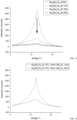
Figure 1 is a graph showing the result of a XRD omega scan for (009) peak of crystalline Sb2Te3 layers with Si doping at 12 at. % (curve with long dashes and dots) and without Si doping (curve with dashes) deposited on native silicon oxide of a silicon wafer substrate. -
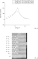
Figure 2 is a graph showing the result of XRD spectra for a multi-layers (ML) based on Ge2Sb2Te5 and Sb2Te3 doped with 12 at. % of Si; the ML without UL (curve with long dashes and dots) shows a very poor crystallinity (i.e. with no texture) whereas the ML with UL (curve with dashes) shows a crystallinity (i.e. a texture). -
Figure 3 is a graph showing the result of a XRD omega scan at 2Theta=25.5°of a ML with Ge2Sb2Te5:Si thickness of 3.6 nm alternate with Sb2Te3 thickness of 2 nm on Sb2Te3 buffer layer (6.3nm). -
Figure 4 is a graph showing the result of a XRD omega scan at 2Theta=25.5° of a ML with Ge2Sb2Te5:Si12% with a thickness of 1.8 nm (top curve) or 3.6 nm (bottom curve) alternates with Sb2Te3 (1 nm and 2 nm) on Sb2Te3 buffer (6.3 nm). -
Figure 5 is a graph showing the result of a XRD omega scan at 2Theta=25.5° of a ML with Ge2Sb2Te5:Si12% with a thickness of 3.6 nm alternates with Sb2Te3 2 nm or 6 nm on Sb2Te3 buffer (6.3 nm). -
Figure 6 is a TEM image of a ML made by alternation of Ge2Sb2Te5:Si8% (3.6nm) and Sb2Te3 (2.1 nm) over a buffer layer Sb2Te3 (6.3nm). The total ML thickness is about 50 nm. -
Figure 7 is a TEM image of a ML made by alternation of Sb2Te3:Si12% (2.1 nm) Ge2Sb2Te5 (3.6 nm) and over a buffer consisting in a bilayer made of Sb2Te3 (6.3 nm) and Ge2Sb2Te5 (3.6 nm). The total ML thickness is around 50 nm. -
Figure 8 is a TEM image of a ML Sb2Te3:Si12% (2.1 nm) Ge2Sb2Te5 (3.6 nm) and over a buffer layer Sb2Te3 (6.3 nm).Figure 8 shows magnification of the crystalline structure. -
Figure 9 is a graph showing the result of a XRD omega scan at 2Theta=25.5° of a ML with Sb2Te3:Si12% with a thickness of 2.1 nm alternates with Ge2Sb2Te5 3.6 nm on Sb2Te3 buffer (6.3 nm) as deposited and after annealing at 400°C for 15 minutes. -
Figure 10 is a graph showing the result of a XRD 2Theta-Theta scan of a ML with Sb2Te3:Si12% with a thickness of 2.1 nm alternates with Ge2Sb2Te5 3.6 nm on Sb2Te3 buffer (6.3 nm) as deposited and after annealing at 400°C for 15 minutes. -
Figure 11 is a TEM image of a ML with Sb2Te3:Si12% with a thickness of 2.1 nm alternated with Ge2Sb2Te5 3.6 nm on Sb2Te3 buffer (6.3 nm) after annealing at 400°C for 15 minutes. -
Figure 12 is an EDX image of a ML with Sb2Te3:Si12% with a thickness of 2.1 nm alternated with Ge2Sb2Te5 3.6 nm on Sb2Te3 buffer (6.3 nm) after annealing at 400°C for 15 minutes. A uniform distribution of all the elements is observed. -
Figure 13 is a TEM image of a ML made by alternation of Ge2Sb2Te5:Si8% (3.6 nm) and Sb2Te3 (2.1 nm) over a buffer layer Sb2Te3 (6.3 nm) after annealing at 400°C for 15 minutes. The arrows indicate the presence of 3-tuple, with the appearing of the new feature. -
Figure 14 is a TEM image at higher resolution of a ML made by alternation of Ge2Sb2Te5:Si8% (3.6 nm) and Sb2Te3 (2.1 nm) over a buffer layer Sb2Te3 (6.3 nm) after annealing at 400°C for 15 minutes. This image shows detail of the new appeared feature. -
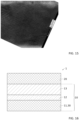
Figure 15 is a TEM image of a GeSb2Te4 layer deposited at 225°C without UL doped with 5 at. % of Si after annealing at 400°C; The texture of the layer is impossible to achieve. -
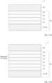
Figure 16 is a first example of a material stack according to the invention in between top and bottom electrodes for a PCM device. -
Figure 17A is a second example of a material stack according to the invention in between top and bottom electrodes; More particularly, said second example comprises, over the UL, a bilayer where the PCM material is a chalcogenide crystalline layer. -
Figure 17B is a variant of the second example illustrated onfigure 17A wherein two or more bilayers can be used and repeated n times. -
Figure 18A is a third example of a material stack according to the invention in between top and bottom electrodes; More particularly, said third example comprises a crystalline Si-doped PCM layer over the UL , followed by a bilayer consisting in a undoped layer of PCM material and a second crystalline Si-doped PCM layer with different Si content or chalcogenide composition. -
Figure 18B is a variant of the third example illustrated onfigure 18A wherein two or more bilayers can be used and repeated n times which are based on the same material as the UL or on different ones. - The drawings are provided as examples and do not limit the invention. They form schematic principle representations intended to facilitate the understanding of the invention and are not necessarily to the scale of the practical applications. In particular, the thicknesses of the different illustrated layers are not necessarily representative of reality or of realistic shape factors.
- Before starting a detailed review of embodiments of the invention, optional features that could possibly be used in combination or alternatively are set out hereinafter.
- As an example of the first aspect of the invention, each undoped crystalline layer may be based on a material allowing its heterogenous epitaxial growth on the substrate and allowing the heterogenous epitaxial growth of the Si-doped crystalline chalcogenide layer thereon.
- As another example of the first aspect of the invention, said first undoped crystalline layer has a crystalline orientation along the (00I) planes.
- As another example of the first aspect of the invention, said undoped crystalline layer may have a stoichiometric composition allowing a deviation of plus or minus 2 at. %, preferably 1 at. %, from a targeted stoichiometric composition, preferably from a perfect one.
- As another example of the first aspect of the invention, said undoped crystalline layer may be an undoped crystalline chalcogenide layer, preferably this latter being a chalcogenide material different or same from the one of said Si-doped crystalline chalcogenide layer.
- As another example of the first aspect of the invention, the material stack may further comprise:
- a. A second undoped crystalline layer over said Si-doped crystalline chalcogenide layer, with said second undoped crystalline layer having a thickness comprised in between 1 and 20 nm and being preferably based on a chalcogenide material, and
- b. A secondary Si-doped crystalline chalcogenide layer over said second undoped crystalline layer, with said secondary Si-doped crystalline chalcogenide layer being based on the same chalcogenide material than said Si-doped crystalline chalcogenide layer.
- As an alternative example of the first aspect of the invention with respect to the preceding one, the material stack may further comprise:
- a. a second undoped crystalline layer over said Si-doped crystalline chalcogenide layer, with said second undoped crystalline layer having a thickness comprised in between 1 and 20 nm and being preferably based on a chalcogenide material, and
- b. at least one sub-stack over said second undoped crystalline layer, each sub-stack comprising:
- i. A secondary Si-doped crystalline chalcogenide layer, and
- ii. A secondary undoped crystalline layer over said secondary Si-doped crystalline chalcogenide layer,
- As an alternative example of the first aspect of the invention with respect to the two preceding ones, the material stack may further comprise:
- a. A second undoped crystalline layer over said Si-doped crystalline chalcogenide layer, with said second undoped crystalline layer having a thickness comprised in between 1 and 20 nm and being preferably based on a chalcogenide material, and
- b. a secondary Si-doped crystalline chalcogenide layer over said second undoped crystalline layer, with said secondary Si-doped crystalline chalcogenide layer being based on a different chalcogenide material than the one of said Si-doped crystalline chalcogenide layer and/or having a different concentration of Si dopants than the one of said Si-doped crystalline chalcogenide layer.
- As an alternative example of the first aspect of the invention with respect to the three preceding ones, the material stack may further comprise:
- a. a second undoped crystalline layer over said Si-doped crystalline chalcogenide layer, with said second undoped crystalline layer having a thickness comprised in between 1 and 20 nm and being preferably based on a chalcogenide material, and
- b. at least one sub-stack over said second undoped crystalline layer, each sub-stack comprising:
- i. A secondary Si-doped crystalline chalcogenide layer, and
- ii. A secondary undoped crystalline layer over said secondary Si-doped crystalline chalcogenide layer,
- with at least one secondary Si-doped crystalline chalcogenide layer being based on a different chalcogenide material than the one of said Si-doped crystalline chalcogenide layer and/or having a different concentration of Si dopants than the one of said Si-doped crystalline chalcogenide layer.
- As a further example of the first aspect of the invention and in relation with the three preceding ones, the material stack may further comprise more than one sub-stack. The sub-stacks are preferably subsequently and directly stacked on each other. More particularly, several sub-stacks are stacked on each other until a total thickness of at least 20 nm, preferably 50 nm or more, of the material stack is reached.
- As another example of the first aspect of the invention, said first undoped crystalline layer extending on the substrate may have a thickness comprised in between 4 and 20 nm, preferably in between 4 and 10 nm.
- As another example of the first aspect of the invention, each Si-doped crystalline chalcogenide layer and/or each undoped crystalline chalcogenide layer may be based on a material chosen among:
- a. GexSbyTez (GST) where "x-y-z" are chosen to reach a stoichiometric composition (such as "2-2-5", "1-2-4", "1-4-7"; etc.) allowing a deviation of plus or minus 2 at. %, preferably 1 at. %, from a targeted stoichiometric composition, preferably from a perfect one,
- b. GeTe, and
- c. Sb2Te3.
- As another example of the first aspect of the invention, each first undoped crystalline layer extending on the substrate may be based on at least one material chosen among:
- a. Sb2Te3,
- b. Bi2Te3, and
- c. Sb2Se3.
- As another example of the first aspect of the invention, said Si-doped crystalline chalcogenide layer may be doped with Si having an atomic concentration ranging from 0.5 to 20 at. %, and preferably from 2 to 18 at. %, and even more preferably from 2 to 12 at. %.
- As another example of the first aspect of the invention, each Si-doped crystalline chalcogenide layer may have a thickness comprised in between 0,5 and 20 nm, preferably in between 1 and 6 nm.
- As another example of the first aspect of the invention, said Si-doped crystalline chalcogenide layer may extend directly on the first undoped crystalline layer.
- As another example of the first aspect of the invention, the substrate comprises a heater, and the first undoped crystalline layer is over the heater.
- As an example of the second aspect of the invention, said thermally processed Si-doped crystalline chalcogenide layer may have a thickness comprised in between 5 and 100 nm, preferably in between 10 and 100 nm, and even more preferably in between 20 and 80 nm, typically equal to 50 nm.
- As an example of the fourth aspect of the invention, the step of providing a material stack may comprise at least:
- a. Providing the substrate,
- b. Depositing, on the substrate, a first undoped crystalline layer having a thickness superior to 4 nm, and
- c. Depositing, by sputtering or co-sputtering at a temperature comprised in between 150 and 300°C, on the first undoped crystalline layer, a Si-doped crystalline chalcogenide layer doped with less than 20 at.%, and preferably less than 12 at.%, of Si and having a thickness equal to or less than 20 nm.
- More generally, the step of providing a material stack may comprise anyone of the steps of the method for manufacturing a material stack according to the first aspect of the invention.
- As an example of the fourth aspect of the invention, the step of thermal treatment is performed at a temperature comprised in between 200 and 500°C, preferably in between 300 and 400°C.
- As an example of the fourth aspect of the invention, said step of thermal treatment is part of an integration process of the material stack in a microelectronic device.
- As an example of the fourth aspect of the invention, said step of thermal treatment is such that, once thermally processed, said Si-doped crystalline chalcogenide layer has a crystal surface parallel to the substrate equal to or greater than 400 nm2, preferably equal to or greater than 20 nm x 20 nm. The crystal orientation allows a deviation of less than 10° with respect to the substrate.
- As an example of the fourth aspect of the invention, said provided material stack comprises a substrate and a multilayer extending on the substrate, said multilayer comprising a plurality of Si-doped crystalline chalcogenide layers and undoped crystalline chalcogenide layers and having a global thickness comprised in between 5 and 100 nm, preferably in between 10 and 100 nm, and even more preferably in between 20 and 80 nm, typically equal to 50 nm.
- By a parameter "equal/greater/less than" a given value is meant that this parameter is equal/greater/less than the given value, to plus or minus 20%, or even 10%, close to this value. A parameter "comprised in between" two given values is meant that this parameter is at least equal to the smallest given value, to plus or minus 20%, or even 10%, near this smallest value, and at most equal to the largest given value, plus or minus 20%, or even 10%, close to this largest value.
- A layer or film based on a material A is understood to mean a film comprising this material A and possibly other materials.
- A crystalline material, or layer, is a solid material, or layer, whose constituents (such as atoms, molecules, or ions) are arranged in a highly ordered microscopic structure, forming a crystal lattice that extends in all directions. A crystalline material, or layer, thus distinguishes from an amorphous material, or layer, and from a polycrystalline material, or layer. All through the present application, word "crystalline" for specifying a material or a layer may mean "formed of crystals having a specific size equal to or greater than 20 nm in x and y directions (parallel to the substrate surface), if needed notably for better distinguishing said crystalline material, or layer, from said polycrystalline material, or layer. Otherwise, the term "textured" is used to qualify a material exhibiting a crystalline arrangement along a specific direction.
- A monocrystalline material, or layer, is a material, or layer, at least 90% of the structure of which is oriented in the same direction. In the context of the present invention, the first undoped layer is monocrystalline. In the following, the terms "monocrystalline" and "crystalline" are used synonymously when referring to this first undoped layer and possibly to the Si-doped chalcogenide layer.
- Epitaxy is a well-known phenomenon of material growth. It is common in minerals which often exhibit special orientation relationships of their lattices. Heteroepitaxy or heterogenous epitaxy is a special case of heterogeneous nucleation in which a distinct crystallographic relationship exists between the orientations of the material of the under layer and the material which is deposited on it. Thus, heteroepitaxy refers to the heterogeneous epitaxial growth of a deposit on an (under)layer of a different material and the formation of bonds at the surfaces between the two materials. A specific type of heteroepitaxy is the Van der Waals epitaxy that refers to the growth mechanism in which the layers are bond together via van der Waals-type weak interactions. This results in far small lattice-mismatch distortion in the grown film even if it has a different lattice constant. In the following, we will refer to heteroepitaxy for the van der Waals type growth.
- By a "chalcogenide" layer is meant a layer made of a material based on chemical elements in
group 16 of the periodic table, and more particularly based on at least one of the following chemical elements: sulfur (S), selenium (Se) and tellurium (Te). - When a sub-stack or a layer is extending or stacked "directly" onto another sub-stack or layer, it means that there is no intermediate layer or sub-stack therebetween.
- The detailed description below is concerned by a
material stack 10 for a Phase-Change Memory (PCM)device 1 as illustrative embodiment only, since thematerial stack 10 according to the first aspect of the invention may alternatively be dedicated to different kinds ofmicroelectronic devices 1 as well, and notably to photonics or RF switches microelectronic devices. - We discuss below the set of conditions for growing a crystalline chalcogenide phase-change material doped with silicon.
- The silicon doping is a source of disorder in the crystalline PCM, as highlighted above, so that the adding of a doping to a chalcogenide material such as Sb2Te3 layer could likely perturb its crystalline arrangement, giving rise to a polycristalline material with short range order (below 10 nm), as known from literature and confirmed by the inventor's experiment illustrated on
Figure 1 showing that Si doping induces high disorder during deposition, leading to the loss of the high texture along the 00I direction. - A big challenge is to make these layers keeping their crystalline arrangement after a BEOL thermal budget (i.e. at 400°C).
- For achieving this purpose, and by reference to
Figures 16 to 18B , the use of a firstundoped crystalline layer 12, as a buffer layer or equivalently as an under-layer (UL), is provided. Said firstundoped crystalline layer 12 has a thickness of few nm (≥ 4 nm) and may be based on a chalcogenide material, such as (but not limited to) Sb2Te3, which shows crystalline arrangement along (00I) planes. The deposition of the firstundoped crystalline layer 12 may be done at a deposition temperature in the range 150°C ≤ T ≤ 300°C. This is a typical range for PVD (physical vapor deposition) process, but the first undoped crystalline layer 12 (also called hereafter "under-layer" or "UL") can be deposited with whatever other technique, with the condition to achieve a stoichiometry and crystalline arrangement. For instance, CVD (chemical vapor deposition), ALD (atomic layer deposition), IBD (ion beam deposition), PLD (pulsed laser deposition), MBE (molecular-beam epitaxy), etc. are possible deposition techniques. - A minimal crystalline arrangement degree is greatly preferred to ensure the growth of a Si-doped
crystalline chalcogenide layer 13 on the under-layer 12. - Others chalcogenide materials can be used for the under-
layer 12 such as Bi2Te3, Sb2Se3, etc. - On the top of the under-
layer 12, it is possible to deposit a chalcogenide layer which has the same crystalline orientation as the under-layer. The crystalline orientation of the under-layer 12 is preferably along the (00I) planes. The introduction of a dopant in the grown chalcogenide layer, could affect the right growth of the chalcogenide layer, therefore a set of specific precautions should be adopted. - It is possible to dope with silicon (Si) most of the chalcogenide materials used for PCM fabrication, such as (but not limited to) GexSbyTez (where "x-y-z" are favorably chosen to reach stoichiometric compositions such as "2-2-5", "1-2-4", "1-4-7" etc.), GeTe, Sb2Te3, etc.
- The deposition of the Si-doped
crystalline chalcogenide layer 13 has to be done at a temperature at which the layer material is deposited under its crystalline form that is at a temperature approximately equal to 225°C, typically at a deposition temperature comprised in between 150 and 300°C. - The crystalline arrangement of the Si-doped
crystalline chalcogenide layer 13 does not depend on the material of the substrate 11 on which the deposition is done, as long as the under-layer 12 can accommodate the ordered crystalline orientation. The presence of the under-layer 12 is mandatory to obtain the Si-dopedcrystalline chalcogenide layer 13 which has a satisfying crystalline arrangement. - Note here that, in case of PCM fabrication, the deposition of said under-
layer 12 and said Si-dopedcrystalline chalcogenide layer 13 is generally done on a substrate 11 having a heterogeneous surface composed by metals such as TiN, W, TaN, etc. and dielectrics such as SiO2, SiN, SiC, etc. The largest area on which said under-layer 12 and said Si-dopedcrystalline chalcogenide layer 13 are deposited may thus be based on an amorphous dielectric material such as SiN or SiO2. - The Si-doped
crystalline chalcogenide layer 13 thus deposited has a high crystalline arrangement close to the one of the under-layer 12. - It could be that, moving far from the under-
layer 12 along the z direction (perpendicular to the plan of main extension of each layer of the material stack 10), the Si-dopedcrystalline chalcogenide layer 13 will stay crystalline but with a more and more degraded crystalline arrangement, or even a polycrystalline arrangement, if the thickness of thelayer 13 is grown to be superior to 20 nm. - In order to increase the thickness along which the crystalline arrangement is propagated, and with references to
Figure 17A , it is further possible to deposit a secondundoped crystalline layer 14 over said Si-dopedcrystalline chalcogenide layer 13, and then deposit, on top oflayer 14, a secondary Si-doped crystalline chalcogenide layer 13' based on the same material than the one of said Si-dopedcrystalline chalcogenide layer 13 and having the same concentration of Si dopants. - As illustrated on
figure 17B , in order to further increase the thickness along which the crystalline arrangement is propagated, it is also possible to repeat n times depositions of pair(s) of secondary layers 13' and 14' on top of said secondundoped crystalline layer 14, if needed before depositing a last secondary Si-doped crystalline chalcogenide layer 13' to form the top layer of thematerial stack 10. For instance, it is thus possible to repeat such deposits until a total thickness of 100 nm or more of thematerial stack 10 is reached. - Said second
undoped crystalline layer 14 may have a thickness comprised in between 1 and 20 nm, in order to be textured in a same direction as the under-layer 12. Otherwise, said secondundoped crystalline layer 14 is preferably based on a chalcogenide material. For instance, the chalcogenide material of the second undopedcrystalline chalcogenide layer 14 may be different from, or the same than, the one of said Si-dopedcrystalline chalcogenide layer 13. This type of structure, shown onFigures 17A and 17B , will be called in the following multi-layer (or ML), in particular by opposition to the embodiment shown onfigure 16 . - As an alternative to the bi-layer embodiment shown on
figure 17A , and with references toFigure 18A , it is possible to deposit, on the secondundoped crystalline layer 14, a secondary Si-doped crystalline chalcogenide layer 15 (instead of the one referred to bynumeral reference 13 onfigure 17A ), with the chalcogenide material of the secondary Si-dopedcrystalline chalcogenide layer 15 being different from the one of said Si-dopedcrystalline chalcogenide layer 13 deposited on theUL 12 and/or having a different concentration of Si dopants than the one of said Si-dopedcrystalline chalcogenide layer 13. - As an alternative to the ML as shown on
figure 17B , and with references toFigure 18B , it is further possible to alternate secondary undoped crystalline layers 14' (that could range, dependently on the chosen layer, from 1 nm up to 20 nm) and secondary Si-doped crystalline chalcogenide layer(s) 15, 16, 17, etc. (that could range, dependently on the chosen layer, from 0.5 nm up to 20 nm) for achieving a ML textured in a same direction as the under-layer 12 and with: - the chalcogenide material of each of the secondary Si-doped crystalline chalcogenide layers 16, 17, etc. being different from, or the same than, the one of said secondary Si-doped
crystalline chalcogenide layer 15 or said Si-dopedcrystalline chalcogenide layer 13 deposited on theUL 12, and/or - at least one of the secondary Si-doped crystalline chalcogenide layers 16, 17, etc. having a concentration of Si dopants different:
- ∘ from each other, or
- ∘ from said secondary Si-doped
crystalline chalcogenide layer 15, or - ∘ from said Si-doped
crystalline chalcogenide layer 13 deposited on theUL 12.
- The higher the thickness of the undoped Si-doped crystalline chalcogenide layer(s) 14', etc., the higher is the control of the crystalline arrangement in the
material stack 10 with larger total thickness (i.e. thickness along which the crystalline arrangement is propagated). - This possibility of growing a
stack 10 as shown onFigure 16 or a multi-layer as shown onFigures 17A and 17B with crystalline arrangement has been demonstrated by the inventors in a cosputtering deposition chamber with a process temperature of 210°C, where the used under-layer 12 has a thickness of approximately 6 nm and was made of Sb2Te3 showing a crystalline orientation along the (00I) planes. - More particularly, as per the embodiment shown on
Figure 16 , the growing of the under-layer 12 with crystalline arrangement has been done by cosputtering of Sb2Te3 and Te target(s) to obtain a sufficiently, or even perfectly, stoichiometric film, and the Si-dopedcrystalline chalcogenide layer 13 was based on either Sb2Te3 or Ge2Sb2Te5 (GST) and obtained by the co-sputtering of the chalcogenide target with a Si target. - In order to enhance the crystalline arrangement of the Si-doped crystalline chalcogenide layers and of the undoped crystalline layers, we may deposit: firstly, the under-
layer 12 on the substrate 11 and then we may alternate Ge2Sb2Te5 and Sb2Te3, by doping with Si the first deposited one among these two chalcogenide materials. - The Si doping was obtained by the cosputtering of the stoichiometric chalcogenide material with a silicon target. The Si doping range may be modulated by changing the applied power on the silicon target. The single layer thickness may be varied from approximately 1 nm up to approximately 6 nm according to the studied structure.
- The demonstration of the possibility to obtain a textured ML doped with Si, is shown in the XRD (X-ray Powder Diffraction) spectra as illustrated on
Figure 2 , in which the ML without under-layer (curve with long dashes and dots) shows a poor crystallinity while the one with under-layer 12 (curve with dashes) shows very intense peaks: it certifies the high degree of crystallinity of the ML (i.e. crystalline arrangement is preserved despite the Si doping). The quality of the crystallinity was also confirmed by TEM images (SeeFig. 6 ,7 and 8 ). - The Si doping range that can allow obtaining textured materials is comprised in between 0.5 and 20 at. % of Si.
- More particularly, in the above-mentioned experiment, the upper limit for a Si-doped
chalcogenide layer 13 based on Ge2Sb2Te5 is about 15 at. % of Si. - One way to investigate if the Si-doped chalcogenide layers are textured is the XRD measurement, and more particularly an omega scan at 2Theta angle position of the main peak (equal to 25.5°) for this kind of composition.
Figure 3 shows the impact of the Si doping on such ML structure composed by an under-layer 12 of Sb2Te3 textured along the (00I) planes and alternating layers of Ge2Sb2Te5 (doped with different at. % of Si) with a thickness of approximately 3.6 nm and Sb2Te3 (undoped) with a thickness of approximately 2.1 nm, and a total thickness of about 50 nm (total thickness of the deposited multilayer). We observe that the height of the peak decreases as the atomic percentage of Si dopants increases. This flattening of the omega scans, notably above 12 at. % of Si and below 18 at. % of Si, leads to the upper bound limit for the Si doping in this configuration at about 15 at. % of Si. -
Figure 4 shows the impact of the thickness of thematerial stack 10 as illustrated onFigure 17A : if the Si-doped Ge2Sb2Te5 layer 13 is thinner (for instance 1.8 nm instead of 3.6 nm), the crystalline arrangement degree is higher (the peak of the curve with dots ofFigure 4 is more intense). The under-layer 12 and more generally at least one of the undoped layer(s) 12, 14, and 14' as illustrated onFigures 16 ,17A ,17B ,18A and 18B has also an important role. For instance, if we increase the thickness(es) of at least one of theundoped layers Figure 5 wherein the less intense peak (curve with dashes) has been obtained for a secondundoped crystalline layer 14 of Sb2Te3 of a thickness equal to 2 nm and the more intense peak (curve with long dashes and dots) has been obtained for a secondundoped crystalline layer 14 of Sb2Te3 of a thickness equal to 6 nm, both structures deposited on a under-layer 12 of Sb2Te3 equal to 6.3nm and alayer 13 of GSTSi of 3.6nm. - The TEM image of
Figure 6 shows, for a multilayer made of undoped Sb2Te3 layers 14, 14' and Ge2Sb2Te5:Si8% (i.e. Ge2Sb2Te5 doped with 8 at. % of Si) layers 13, 13', how the multilayer is crystalline with high orientation over the total thickness of 50 nm of the multilayer. - In the case of Sb2Te3 as based material for the Si-doped chalcogenide layer(s) 13, 13' the upper limit of Si doping is about 20 at. % of Si. The same proof than for GST can be provided. The TEM images of
Figure 7 and Figure 8 show the highly textured as-deposited multilayer obtained by the alternated deposition of undoped Ge2Sb2Te5 14, 14' with a thickness of approximately 3.6 nm and Si-doped Sb2Te3:Si12% layer(s) 13, 13' with a thickness of approximately 2.1 nm on an under-layer layer 12 at least partially based on Sb2Te3. In this particular case, the secondundoped crystalline layer 14 is deposited before the Si-dopedchalcogenide layer 13, but it maintains the same crystalline orientation as theUL 12. This configuration represents a possible variant of the stacking. Otherwise, the example shown onFigure 7 allows illustrating that theUL 12 is not necessarily made of a single layer but can also take the form of a multilayer. Indeed, according to the example shown onfigure 7 , the underlayer is a bilayer made of a first layer based on Sb2Te3 extending on the substrate 11 and of a second layer based on Ge2Sb2Te5 extending on the first layer. It should be noted that, in the case of an under-layer 12 taking the form of a bilayer, the second layer is preferably of a thickness less than or equal to half the thickness of the underlying layer. - From inventor's experience, further thermally treating the multilayer at 400°C for 15 minutes, thus achieving a thermally processed material stack according to the second aspect of the invention, does not degrade the crystalline arrangement as can be seen by the XRD omega scan shown on
Figure 9 of a multilayer with Si-doped Sb2Te3:Si12% layer(s) 13, 13' with a thickness of approximately 2.1 nm and undoped Ge2Sb2Te5 layers 14, 14' with a thickness of approximately 3.6 nm over an under-layer 12 of Sb2Te3 with a thickness of approximately 6.3 nm; indeed, where the curve with dashes is obtained by XRD omega scan of thematerial stack 10 as deposited, that is before any thermal treatment, and the curve with long dashes and dots is obtained by XRD omega scan of thematerial stack 10 after thermal treatment, the curves are not significantly different from each other. - The XRD 2Theta-Theta scan as illustrated on
Figure 10 shows how thematerial stack 10 rearranges: this phenomenon induces the enhancement and the shift of certain XRD peaks. - In the TEM image of
Figure 11 , it can be noticed that the multilayer keeps the crystalline arrangement along the z direction, and we can recognize the alternation of atomic blocks separated by Van Der Waals (VdW) gaps. - As illustrated on
Figure 12 , the EDX images of thematerial stack 10 after thermal treatment, that is the EDX images of the thermally processed material stack according to the second aspect of the invention, show that the composition of the thermally treated stack is uniform along its thickness losing the multi-layer structure. Also, the silicon is uniformly distributed, without the appearing of any precipitation, which means that the Si dopants accommodate in the crystalline chalcogenide layers 13, 13', 14, and 14'. - It was also noticed that the doping of Ge2Sb2Te5 material with 8 at. % of Si for manufacturing the Si-doped crystalline chalcogenide layer(s) 13, 13', gives rise to the appearing of a new feature as shown for instance on
Figures 13 and 14 . The TEM images illustrated onFigures 13 and 14 show the presence of new atomic arrangement with 3-tuple which is not characteristics of any GexSbyTez crystalline block. This new feature can probably be induced by the creation of Si-Te bonds and so the arrangement of Si atoms between Te planes, confirming the perfect incorporation of Si in the crystalline structure of the Si-doped chalcogenide layer(s) 13, 13'. - As a comparison with respect to what previously shown, in
Figure 15 is shown the TEM image of a GST124 layer doped with Si deposited on a SiN substrate 11, without under-layer and after annealing at 400°C. The GST124 layer does not show any crystalline arrangement (not even in a direction different from the z one), but only a polycrystalline structure. - The invention is not limited to the embodiments previously described and extends to all the embodiments covered by the claims.
Claims (15)
- A material stack (10) for microelectronic device (1) comprising:a. A substrate (11),b. A first undoped monocrystalline layer (12) on the substrate, said undoped monocrystalline layer having a thickness superior or equal to 4 nm, andc. A Si-doped crystalline chalcogenide layer (13) on the first undoped monocrystalline layer, said Si-doped crystalline chalcogenide layer being doped with Si having an atomic concentration ranging from 0.5 at.% to 20 at.%, and preferably from 2 at.% to 12 at.%, and said Si-doped crystalline chalcogenide layer (13) having a thickness comprised in between 0.5 nm and 20 nm.
- The material stack (10) according to the preceding claim, wherein the first undoped monocrystalline layer (12) is based on a material allowing its heterogenous epitaxial growth on the substrate (11) and allowing the heterogenous epitaxial growth of the Si-doped crystalline chalcogenide layer (13) thereon.
- The material stack (10) according to anyone of the preceding claims, wherein said first undoped monocrystalline layer (12) is an undoped monocrystalline chalcogenide layer.
- The material stack (10) according to anyone of the preceding claims, wherein the Si-doped chalcogenide layer (13) is monocrystalline.
- The material stack (10) according to anyone of the preceding claims, wherein the first undoped layer (12) is monocrystalline as deposited on the substrate, and wherein the Si-doped chalcogenide layer (13) is crystalline as deposited on the first undoped monocrystalline layer.
- The material stack (10) according to anyone of the preceding claims, further comprising:a. A second undoped crystalline layer (14) over said Si-doped crystalline chalcogenide layer (13), with said second undoped crystalline layer (14) having a thickness comprised in between 1 and 20 nm and being preferably based on a chalcogenide material, andb. A secondary Si-doped crystalline chalcogenide layer (13') over said second undoped crystalline layer (14), with said secondary Si-doped crystalline chalcogenide layer (13') being based on the same chalcogenide material than said Si-doped crystalline chalcogenide layer (13).
- The material stack (10) according to anyone of claims 1 to 5, further comprising:a. a second undoped crystalline layer (14) over said Si-doped crystalline chalcogenide layer (13), with said second undoped crystalline layer (14) having a thickness comprised in between 1 and 20 nm and being preferably based on a chalcogenide material, andb. a secondary Si-doped crystalline chalcogenide layer (15) over said second undoped crystalline layer (14), with said secondary Si-doped crystalline chalcogenide layer (15) being based on a different chalcogenide material than the one of said Si-doped crystalline chalcogenide layer (13) and/or having a different concentration of Si dopants than the one of said Si-doped crystalline chalcogenide layer (13).
- The material stack (10) according to anyone of the preceding claims, wherein the substrate (11) comprises a heater, and wherein the first undoped crystalline layer (12) is over the heater.
- The material stack (10) according to anyone of the preceding claims, wherein each Si-doped crystalline chalcogenide layer (13, 13', 15, 16, 17) and/or each undoped crystalline chalcogenide layer (14, 14') is based on a material chosen among:a. GexSbyTez (GST) where "x-y-z" are chosen to reach a stoichiometric composition allowing a deviation of plus or minus 2 at. %, preferably 1 at. %, from a targeted stoichiometric composition,b. GeTe, andc. Sb2Te3.
- The material stack (10) according to anyone of the preceding claims, wherein each first undoped crystalline layer (12) extending on the substrate (11) is based on at least one material chosen among:a. Sb2Te3,b. Bi2Te3, andc. Sb2Se3.
- A thermally processed material stack for microelectronic device (1), such as a Phase-Change Memory (PCM) device, comprising:a. A substrate (11), andb. A thermally processed Si-doped crystalline chalcogenide layer on the substrate (11), said thermally processed Si-doped crystalline chalcogenide layer being doped with less than 20 at.%, and preferably less than 12 at.%, of Si and said thermally processed Si-doped crystalline chalcogenide layer having a crystal surface parallel to the substrate equal to or greater than 400 nm2, preferably equal to or greater than 20 nm x 20 nm.
- A method for manufacturing a thermally processed material stack comprising:a. A step of providing a material stack (10) according to anyone of claims 1 to 10; andb. A step of thermal treatment of the provided material stack.
- The method according to the preceding claim, wherein said step of thermal treatment is part of an integration process of the material stack (10) in a microelectronic device (1).
- The method according to anyone of the two preceding claims, wherein the Si-doped crystalline chalcogenide layer is formed by co-sputtering deposition.
- A microelectronic device (1), such as a Phase-Change Memory (PCM) device, comprising at least a material stack (10) according to any one of claims 1 to 10 or at least a thermally processed material stack according to claim 11, further comprising a top electrode (20) of the microelectronic device (1) on the material stack, and wherein a substrate (11) of the concerned material stack comprises a bottom electrode (30) of the microelectronic device (1).
Applications Claiming Priority (1)
| Application Number | Priority Date | Filing Date | Title |
|---|---|---|---|
| EP22315346.1A EP4390933A1 (en) | 2022-12-21 | 2022-12-21 | Material stack for microelectronic device, a microelectronic device that integrates such stack and method for manufacturing such stack |
Publications (2)
| Publication Number | Publication Date |
|---|---|
| EP4390936A1 true EP4390936A1 (en) | 2024-06-26 |
| EP4390936B1 EP4390936B1 (en) | 2026-07-01 |
Family
ID=84982395
Family Applications (2)
| Application Number | Title | Priority Date | Filing Date |
|---|---|---|---|
| EP22315346.1A Withdrawn EP4390933A1 (en) | 2022-12-21 | 2022-12-21 | Material stack for microelectronic device, a microelectronic device that integrates such stack and method for manufacturing such stack |
| EP23219178.3A Active EP4390936B1 (en) | 2022-12-21 | 2023-12-21 | Material stack for microelectronic device, microelectronic device with integrated such stack and method for producing such a stack |
Family Applications Before (1)
| Application Number | Title | Priority Date | Filing Date |
|---|---|---|---|
| EP22315346.1A Withdrawn EP4390933A1 (en) | 2022-12-21 | 2022-12-21 | Material stack for microelectronic device, a microelectronic device that integrates such stack and method for manufacturing such stack |
Country Status (2)
| Country | Link |
|---|---|
| US (1) | US20240215466A1 (en) |
| EP (2) | EP4390933A1 (en) |
Citations (3)
| Publication number | Priority date | Publication date | Assignee | Title |
|---|---|---|---|---|
| US20130270503A1 (en) * | 2010-12-17 | 2013-10-17 | Huazhong University Of Science And Technology | Multi-layer phase change material |
| US20220209105A1 (en) * | 2020-12-29 | 2022-06-30 | International Business Machines Corporation | Multi-layer phase change memory device |
| EP4271166A1 (en) * | 2022-04-28 | 2023-11-01 | Commissariat à l'énergie atomique et aux énergies alternatives | Method for manufacturing phase change material |
Family Cites Families (1)
| Publication number | Priority date | Publication date | Assignee | Title |
|---|---|---|---|---|
| US8809829B2 (en) * | 2009-06-15 | 2014-08-19 | Macronix International Co., Ltd. | Phase change memory having stabilized microstructure and manufacturing method |
-
2022
- 2022-12-21 EP EP22315346.1A patent/EP4390933A1/en not_active Withdrawn
-
2023
- 2023-12-21 US US18/393,050 patent/US20240215466A1/en active Pending
- 2023-12-21 EP EP23219178.3A patent/EP4390936B1/en active Active
Patent Citations (3)
| Publication number | Priority date | Publication date | Assignee | Title |
|---|---|---|---|---|
| US20130270503A1 (en) * | 2010-12-17 | 2013-10-17 | Huazhong University Of Science And Technology | Multi-layer phase change material |
| US20220209105A1 (en) * | 2020-12-29 | 2022-06-30 | International Business Machines Corporation | Multi-layer phase change memory device |
| EP4271166A1 (en) * | 2022-04-28 | 2023-11-01 | Commissariat à l'énergie atomique et aux énergies alternatives | Method for manufacturing phase change material |
Non-Patent Citations (7)
| Title |
|---|
| FEGN ET AL.: "Si doping in Ge Sb Te film to reduce the writing current of phase change memory", APPLIED PHYSICS A, vol. 87, 2007, pages 57 - 62, XP019490441, DOI: 10.1007/s00339-006-3851-2 |
| FENG J ET AL: "Si doping in Ge2Sb2Te5 film to reduce the writing current of phase change memory", APPLIED PHYSICS A; MATERIALS SCIENCE & PROCESSING, SPRINGER, BERLIN, DE, vol. 87, no. 1, 1 February 2007 (2007-02-01), pages 57 - 62, XP019490441, ISSN: 1432-0630, DOI: 10.1007/S00339-006-3851-2 * |
| JIANG ET AL.: "Silicon doping effect on the crystallization behavior of Ge2Sb2Te5 film", PHYSICA STATUS SOLIDI (A), APPLICATIONS AND MATERIALS, vol. 210, no. 10, 2013 |
| TOMINAGA ET AL.: "Intermixing suppression through the interface in GeTe/Sb Te superlattice", APPLIED PHYSICS EXPRESS, vol. 13, no. 7 |
| YANG ET AL.: "Effect of Si doping on the structure and optical properties of Ge2Sb2Te5 studied by ab initio calculations", COMPUTATIONAL MATERIALS SCIENCE, vol. 168, 2019, pages 253 - 259, XP085736090, DOI: 10.1016/j.commatsci.2019.05.019 |
| ZHANG ET AL.: "Characteristics of Si-doped Sb2Te3 thin films for phase-change random access memory", APPLIED SURFACE SCIENCE, vol. 254, 2008, pages 5602 - 5606, XP022680665, DOI: 10.1016/j.apsusc.2008.03.006 |
| ZHANG Y ET AL: "Characteristics of Si-doped Sb"2Te"3 thin films for phase-change random access memory", APPLIED SURFACE SCIENCE, ELSEVIER, AMSTERDAM , NL, vol. 254, no. 17, 30 June 2008 (2008-06-30), pages 5602 - 5606, XP022680665, ISSN: 0169-4332, [retrieved on 20080312], DOI: 10.1016/J.APSUSC.2008.03.006 * |
Also Published As
| Publication number | Publication date |
|---|---|
| US20240215466A1 (en) | 2024-06-27 |
| EP4390933A1 (en) | 2024-06-26 |
| EP4390936B1 (en) | 2026-07-01 |
Similar Documents
| Publication | Publication Date | Title |
|---|---|---|
| US20240381660A1 (en) | Memory cell, capacitive memory structure, and methods thereof | |
| Lotnyk et al. | Temperature dependent evolution of local structure in chalcogenide-based superlattices | |
| US7060586B2 (en) | PCMO thin film with resistance random access memory (RRAM) characteristics | |
| US9818939B2 (en) | Resistive switching devices having a switching layer and an intermediate electrode layer and methods of formation thereof | |
| CN109256385A (en) | The manufacturing method of ferroelectric memory device | |
| WO2015196412A1 (en) | Metal doped ge-sb-te-based multivalue storage phase-change material and phase-change memory | |
| CN103069056B (en) | Oxide substrate and method for producing same | |
| US20240114806A1 (en) | Process for manufacturing a phase change material | |
| US11101430B2 (en) | Storage element | |
| Thelander et al. | Low temperature epitaxy of Ge-Sb-Te films on BaF2 (111) by pulsed laser deposition | |
| JP2017045783A (en) | Semiconductor device and manufacturing method thereof | |
| Shen et al. | Effect of crystallinity on the performance of AlN-based resistive random access memory using rapid thermal annealing | |
| Kerres et al. | Growth of textured chalcogenide thin films and their functionalization through confinement | |
| Kolobov et al. | Local structure of the crystalline and amorphous states of Ga 2 Te 3 phase-change alloy without resonant bonding: A combined x-ray absorption and ab initio study | |
| JP5692365B2 (en) | Perovskite-type manganese oxide thin film | |
| EP4390933A1 (en) | Material stack for microelectronic device, a microelectronic device that integrates such stack and method for manufacturing such stack | |
| JP5725036B2 (en) | Perovskite-type manganese oxide thin film and method for producing the same | |
| CN114792754B (en) | Superlattice phase transition structures and their fabrication methods, phase change memory | |
| JP3705695B2 (en) | Method for producing dielectric thin film with layered perovskite structure, dielectric thin film with layered perovskite structure and electronic component having dielectric thin film with layered perovskite structure | |
| US20220020923A1 (en) | Phase-change material and associated resistive phase-change memory | |
| KR20090077232A (en) | Phase change layer and phase change memory device including the same | |
| KR101092424B1 (en) | Method for forming In-Sb-Te thin film by chemical vapor deposition and method for manufacturing phase-change memory device using the same | |
| JP2008187171A (en) | Semiconductor device including polysilicon and method of manufacturing the same | |
| CN114824074B (en) | Phase change material, phase change memory, and preparation method | |
| US20240099166A1 (en) | Boron Surface Passivation of Phase Change Memory Material |
Legal Events
| Date | Code | Title | Description |
|---|---|---|---|
| PUAI | Public reference made under article 153(3) epc to a published international application that has entered the european phase |
Free format text: ORIGINAL CODE: 0009012 |
|
| STAA | Information on the status of an ep patent application or granted ep patent |
Free format text: STATUS: REQUEST FOR EXAMINATION WAS MADE |
|
| 17P | Request for examination filed |
Effective date: 20231221 |
|
| AK | Designated contracting states |
Kind code of ref document: A1 Designated state(s): AL AT BE BG CH CY CZ DE DK EE ES FI FR GB GR HR HU IE IS IT LI LT LU LV MC ME MK MT NL NO PL PT RO RS SE SI SK SM TR |
|
| RAP3 | Party data changed (applicant data changed or rights of an application transferred) |
Owner name: COMMISSARIAT A L'ENERGIE ATOMIQUE ET AUX ENERGIESALTERNATIVES |
|
| STAA | Information on the status of an ep patent application or granted ep patent |
Free format text: STATUS: EXAMINATION IS IN PROGRESS |
|
| 17Q | First examination report despatched |
Effective date: 20250411 |
|
| GRAJ | Information related to disapproval of communication of intention to grant by the applicant or resumption of examination proceedings by the epo deleted |
Free format text: ORIGINAL CODE: EPIDOSDIGR1 |
|
| GRAP | Despatch of communication of intention to grant a patent |
Free format text: ORIGINAL CODE: EPIDOSNIGR1 |
|
| GRAP | Despatch of communication of intention to grant a patent |
Free format text: ORIGINAL CODE: EPIDOSNIGR1 |
|
| STAA | Information on the status of an ep patent application or granted ep patent |
Free format text: STATUS: GRANT OF PATENT IS INTENDED |
|
| INTG | Intention to grant announced |
Effective date: 20260211 |
|
| GRAS | Grant fee paid |
Free format text: ORIGINAL CODE: EPIDOSNIGR3 |
|
| GRAA | (expected) grant |
Free format text: ORIGINAL CODE: 0009210 |
|
| STAA | Information on the status of an ep patent application or granted ep patent |
Free format text: STATUS: THE PATENT HAS BEEN GRANTED |
|
| AK | Designated contracting states |
Kind code of ref document: B1 Designated state(s): AL AT BE BG CH CY CZ DE DK EE ES FI FR GB GR HR HU IE IS IT LI LT LU LV MC ME MK MT NL NO PL PT RO RS SE SI SK SM TR |
|
| REG | Reference to a national code |
Ref country code: CH Ref legal event code: F10 Free format text: ST27 STATUS EVENT CODE: U-0-0-F10-F00 (AS PROVIDED BY THE NATIONAL OFFICE) Effective date: 20260701 Ref country code: GB Ref legal event code: FG4D |
|
| REG | Reference to a national code |
Ref country code: DE Ref legal event code: R096 Ref document number: 602023019169 Country of ref document: DE |
|
| REG | Reference to a national code |
Ref country code: IE Ref legal event code: FG4D |