EP4390474A1 - Colored-layer-forming composition, optical film, and display device - Google Patents
Colored-layer-forming composition, optical film, and display device Download PDFInfo
- Publication number
- EP4390474A1 EP4390474A1 EP22858500.6A EP22858500A EP4390474A1 EP 4390474 A1 EP4390474 A1 EP 4390474A1 EP 22858500 A EP22858500 A EP 22858500A EP 4390474 A1 EP4390474 A1 EP 4390474A1
- Authority
- EP
- European Patent Office
- Prior art keywords
- group
- carbon atoms
- fewer carbon
- layer
- colored layer
- Prior art date
- Legal status (The legal status is an assumption and is not a legal conclusion. Google has not performed a legal analysis and makes no representation as to the accuracy of the status listed.)
- Pending
Links
Images


Classifications
-
- H—ELECTRICITY
- H10—SEMICONDUCTOR DEVICES; ELECTRIC SOLID-STATE DEVICES NOT OTHERWISE PROVIDED FOR
- H10K—ORGANIC ELECTRIC SOLID-STATE DEVICES
- H10K50/00—Organic light-emitting devices
- H10K50/80—Constructional details
- H10K50/86—Arrangements for improving contrast, e.g. preventing reflection of ambient light
-
- C—CHEMISTRY; METALLURGY
- C09—DYES; PAINTS; POLISHES; NATURAL RESINS; ADHESIVES; COMPOSITIONS NOT OTHERWISE PROVIDED FOR; APPLICATIONS OF MATERIALS NOT OTHERWISE PROVIDED FOR
- C09D—COATING COMPOSITIONS, e.g. PAINTS, VARNISHES OR LACQUERS; FILLING PASTES; CHEMICAL PAINT OR INK REMOVERS; INKS; CORRECTING FLUIDS; WOODSTAINS; PASTES OR SOLIDS FOR COLOURING OR PRINTING; USE OF MATERIALS THEREFOR
- C09D4/00—Coating compositions, e.g. paints, varnishes or lacquers, based on organic non-macromolecular compounds having at least one polymerisable carbon-to-carbon unsaturated bond ; Coating compositions, based on monomers of macromolecular compounds of groups C09D183/00 - C09D183/16
- C09D4/06—Organic non-macromolecular compounds having at least one polymerisable carbon-to-carbon unsaturated bond in combination with a macromolecular compound other than an unsaturated polymer of groups C09D159/00 - C09D187/00
-
- C—CHEMISTRY; METALLURGY
- C08—ORGANIC MACROMOLECULAR COMPOUNDS; THEIR PREPARATION OR CHEMICAL WORKING-UP; COMPOSITIONS BASED THEREON
- C08F—MACROMOLECULAR COMPOUNDS OBTAINED BY REACTIONS ONLY INVOLVING CARBON-TO-CARBON UNSATURATED BONDS
- C08F2/00—Processes of polymerisation
- C08F2/44—Polymerisation in the presence of compounding ingredients, e.g. plasticisers, dyestuffs, fillers
-
- C—CHEMISTRY; METALLURGY
- C08—ORGANIC MACROMOLECULAR COMPOUNDS; THEIR PREPARATION OR CHEMICAL WORKING-UP; COMPOSITIONS BASED THEREON
- C08F—MACROMOLECULAR COMPOUNDS OBTAINED BY REACTIONS ONLY INVOLVING CARBON-TO-CARBON UNSATURATED BONDS
- C08F2/00—Processes of polymerisation
- C08F2/46—Polymerisation initiated by wave energy or particle radiation
- C08F2/48—Polymerisation initiated by wave energy or particle radiation by ultraviolet or visible light
- C08F2/50—Polymerisation initiated by wave energy or particle radiation by ultraviolet or visible light with sensitising agents
-
- C—CHEMISTRY; METALLURGY
- C08—ORGANIC MACROMOLECULAR COMPOUNDS; THEIR PREPARATION OR CHEMICAL WORKING-UP; COMPOSITIONS BASED THEREON
- C08F—MACROMOLECULAR COMPOUNDS OBTAINED BY REACTIONS ONLY INVOLVING CARBON-TO-CARBON UNSATURATED BONDS
- C08F220/00—Copolymers of compounds having one or more unsaturated aliphatic radicals, each having only one carbon-to-carbon double bond, and only one being terminated by only one carboxyl radical or a salt, anhydride ester, amide, imide or nitrile thereof
- C08F220/02—Monocarboxylic acids having less than ten carbon atoms; Derivatives thereof
- C08F220/10—Esters
- C08F220/12—Esters of monohydric alcohols or phenols
- C08F220/14—Methyl esters, e.g. methyl (meth)acrylate
-
- C—CHEMISTRY; METALLURGY
- C08—ORGANIC MACROMOLECULAR COMPOUNDS; THEIR PREPARATION OR CHEMICAL WORKING-UP; COMPOSITIONS BASED THEREON
- C08F—MACROMOLECULAR COMPOUNDS OBTAINED BY REACTIONS ONLY INVOLVING CARBON-TO-CARBON UNSATURATED BONDS
- C08F220/00—Copolymers of compounds having one or more unsaturated aliphatic radicals, each having only one carbon-to-carbon double bond, and only one being terminated by only one carboxyl radical or a salt, anhydride ester, amide, imide or nitrile thereof
- C08F220/02—Monocarboxylic acids having less than ten carbon atoms; Derivatives thereof
- C08F220/10—Esters
- C08F220/20—Esters of polyhydric alcohols or phenols, e.g. 2-hydroxyethyl (meth)acrylate or glycerol mono-(meth)acrylate
-
- C—CHEMISTRY; METALLURGY
- C08—ORGANIC MACROMOLECULAR COMPOUNDS; THEIR PREPARATION OR CHEMICAL WORKING-UP; COMPOSITIONS BASED THEREON
- C08F—MACROMOLECULAR COMPOUNDS OBTAINED BY REACTIONS ONLY INVOLVING CARBON-TO-CARBON UNSATURATED BONDS
- C08F220/00—Copolymers of compounds having one or more unsaturated aliphatic radicals, each having only one carbon-to-carbon double bond, and only one being terminated by only one carboxyl radical or a salt, anhydride ester, amide, imide or nitrile thereof
- C08F220/02—Monocarboxylic acids having less than ten carbon atoms; Derivatives thereof
- C08F220/10—Esters
- C08F220/34—Esters containing nitrogen, e.g. N,N-dimethylaminoethyl (meth)acrylate
-
- C—CHEMISTRY; METALLURGY
- C08—ORGANIC MACROMOLECULAR COMPOUNDS; THEIR PREPARATION OR CHEMICAL WORKING-UP; COMPOSITIONS BASED THEREON
- C08F—MACROMOLECULAR COMPOUNDS OBTAINED BY REACTIONS ONLY INVOLVING CARBON-TO-CARBON UNSATURATED BONDS
- C08F265/00—Macromolecular compounds obtained by polymerising monomers on to polymers of unsaturated monocarboxylic acids or derivatives thereof as defined in group C08F20/00
- C08F265/04—Macromolecular compounds obtained by polymerising monomers on to polymers of unsaturated monocarboxylic acids or derivatives thereof as defined in group C08F20/00 on to polymers of esters
- C08F265/06—Polymerisation of acrylate or methacrylate esters on to polymers thereof
-
- C—CHEMISTRY; METALLURGY
- C08—ORGANIC MACROMOLECULAR COMPOUNDS; THEIR PREPARATION OR CHEMICAL WORKING-UP; COMPOSITIONS BASED THEREON
- C08F—MACROMOLECULAR COMPOUNDS OBTAINED BY REACTIONS ONLY INVOLVING CARBON-TO-CARBON UNSATURATED BONDS
- C08F290/00—Macromolecular compounds obtained by polymerising monomers on to polymers modified by introduction of aliphatic unsaturated end or side groups
- C08F290/02—Macromolecular compounds obtained by polymerising monomers on to polymers modified by introduction of aliphatic unsaturated end or side groups on to polymers modified by introduction of unsaturated end groups
- C08F290/06—Polymers provided for in subclass C08G
- C08F290/067—Polyurethanes; Polyureas
-
- C—CHEMISTRY; METALLURGY
- C08—ORGANIC MACROMOLECULAR COMPOUNDS; THEIR PREPARATION OR CHEMICAL WORKING-UP; COMPOSITIONS BASED THEREON
- C08J—WORKING-UP; GENERAL PROCESSES OF COMPOUNDING; AFTER-TREATMENT NOT COVERED BY SUBCLASSES C08B, C08C, C08F, C08G or C08H
- C08J7/00—Chemical treatment or coating of shaped articles made of macromolecular substances
- C08J7/04—Coating
- C08J7/042—Coating with two or more layers, where at least one layer of a composition contains a polymer binder
-
- C—CHEMISTRY; METALLURGY
- C08—ORGANIC MACROMOLECULAR COMPOUNDS; THEIR PREPARATION OR CHEMICAL WORKING-UP; COMPOSITIONS BASED THEREON
- C08J—WORKING-UP; GENERAL PROCESSES OF COMPOUNDING; AFTER-TREATMENT NOT COVERED BY SUBCLASSES C08B, C08C, C08F, C08G or C08H
- C08J7/00—Chemical treatment or coating of shaped articles made of macromolecular substances
- C08J7/04—Coating
- C08J7/044—Forming conductive coatings; Forming coatings having anti-static properties
-
- C—CHEMISTRY; METALLURGY
- C08—ORGANIC MACROMOLECULAR COMPOUNDS; THEIR PREPARATION OR CHEMICAL WORKING-UP; COMPOSITIONS BASED THEREON
- C08J—WORKING-UP; GENERAL PROCESSES OF COMPOUNDING; AFTER-TREATMENT NOT COVERED BY SUBCLASSES C08B, C08C, C08F, C08G or C08H
- C08J7/00—Chemical treatment or coating of shaped articles made of macromolecular substances
- C08J7/04—Coating
- C08J7/046—Forming abrasion-resistant coatings; Forming surface-hardening coatings
-
- C—CHEMISTRY; METALLURGY
- C08—ORGANIC MACROMOLECULAR COMPOUNDS; THEIR PREPARATION OR CHEMICAL WORKING-UP; COMPOSITIONS BASED THEREON
- C08J—WORKING-UP; GENERAL PROCESSES OF COMPOUNDING; AFTER-TREATMENT NOT COVERED BY SUBCLASSES C08B, C08C, C08F, C08G or C08H
- C08J7/00—Chemical treatment or coating of shaped articles made of macromolecular substances
- C08J7/04—Coating
- C08J7/048—Forming gas barrier coatings
-
- C—CHEMISTRY; METALLURGY
- C08—ORGANIC MACROMOLECULAR COMPOUNDS; THEIR PREPARATION OR CHEMICAL WORKING-UP; COMPOSITIONS BASED THEREON
- C08K—Use of inorganic or non-macromolecular organic substances as compounding ingredients
- C08K5/00—Use of organic ingredients
- C08K5/0008—Organic ingredients according to more than one of the "one dot" groups of C08K5/01 - C08K5/59
- C08K5/0041—Optical brightening agents, organic pigments
-
- C—CHEMISTRY; METALLURGY
- C08—ORGANIC MACROMOLECULAR COMPOUNDS; THEIR PREPARATION OR CHEMICAL WORKING-UP; COMPOSITIONS BASED THEREON
- C08K—Use of inorganic or non-macromolecular organic substances as compounding ingredients
- C08K5/00—Use of organic ingredients
- C08K5/0008—Organic ingredients according to more than one of the "one dot" groups of C08K5/01 - C08K5/59
- C08K5/005—Stabilisers against oxidation, heat, light, ozone
-
- C—CHEMISTRY; METALLURGY
- C08—ORGANIC MACROMOLECULAR COMPOUNDS; THEIR PREPARATION OR CHEMICAL WORKING-UP; COMPOSITIONS BASED THEREON
- C08K—Use of inorganic or non-macromolecular organic substances as compounding ingredients
- C08K5/00—Use of organic ingredients
- C08K5/0091—Complexes with metal-heteroatom-bonds
-
- C—CHEMISTRY; METALLURGY
- C08—ORGANIC MACROMOLECULAR COMPOUNDS; THEIR PREPARATION OR CHEMICAL WORKING-UP; COMPOSITIONS BASED THEREON
- C08K—Use of inorganic or non-macromolecular organic substances as compounding ingredients
- C08K5/00—Use of organic ingredients
- C08K5/36—Sulfur-, selenium-, or tellurium-containing compounds
- C08K5/37—Thiols
-
- C—CHEMISTRY; METALLURGY
- C08—ORGANIC MACROMOLECULAR COMPOUNDS; THEIR PREPARATION OR CHEMICAL WORKING-UP; COMPOSITIONS BASED THEREON
- C08K—Use of inorganic or non-macromolecular organic substances as compounding ingredients
- C08K5/00—Use of organic ingredients
- C08K5/36—Sulfur-, selenium-, or tellurium-containing compounds
- C08K5/39—Thiocarbamic acids; Derivatives thereof, e.g. dithiocarbamates
-
- C—CHEMISTRY; METALLURGY
- C08—ORGANIC MACROMOLECULAR COMPOUNDS; THEIR PREPARATION OR CHEMICAL WORKING-UP; COMPOSITIONS BASED THEREON
- C08K—Use of inorganic or non-macromolecular organic substances as compounding ingredients
- C08K5/00—Use of organic ingredients
- C08K5/49—Phosphorus-containing compounds
- C08K5/51—Phosphorus bound to oxygen
- C08K5/52—Phosphorus bound to oxygen only
- C08K5/521—Esters of phosphoric acids, e.g. of H3PO4
-
- C—CHEMISTRY; METALLURGY
- C09—DYES; PAINTS; POLISHES; NATURAL RESINS; ADHESIVES; COMPOSITIONS NOT OTHERWISE PROVIDED FOR; APPLICATIONS OF MATERIALS NOT OTHERWISE PROVIDED FOR
- C09D—COATING COMPOSITIONS, e.g. PAINTS, VARNISHES OR LACQUERS; FILLING PASTES; CHEMICAL PAINT OR INK REMOVERS; INKS; CORRECTING FLUIDS; WOODSTAINS; PASTES OR SOLIDS FOR COLOURING OR PRINTING; USE OF MATERIALS THEREFOR
- C09D135/00—Coating compositions based on homopolymers or copolymers of compounds having one or more unsaturated aliphatic radicals, each having only one carbon-to-carbon double bond, and at least one being terminated by a carboxyl radical, and containing at least another carboxyl radical in the molecule, or of salts, anhydrides, esters, amides, imides or nitriles thereof; Coating compositions based on derivatives of such polymers
- C09D135/02—Homopolymers or copolymers of esters
-
- C—CHEMISTRY; METALLURGY
- C09—DYES; PAINTS; POLISHES; NATURAL RESINS; ADHESIVES; COMPOSITIONS NOT OTHERWISE PROVIDED FOR; APPLICATIONS OF MATERIALS NOT OTHERWISE PROVIDED FOR
- C09D—COATING COMPOSITIONS, e.g. PAINTS, VARNISHES OR LACQUERS; FILLING PASTES; CHEMICAL PAINT OR INK REMOVERS; INKS; CORRECTING FLUIDS; WOODSTAINS; PASTES OR SOLIDS FOR COLOURING OR PRINTING; USE OF MATERIALS THEREFOR
- C09D5/00—Coating compositions, e.g. paints, varnishes or lacquers, characterised by their physical nature or the effects produced; Filling pastes
- C09D5/006—Anti-reflective coatings
-
- C—CHEMISTRY; METALLURGY
- C09—DYES; PAINTS; POLISHES; NATURAL RESINS; ADHESIVES; COMPOSITIONS NOT OTHERWISE PROVIDED FOR; APPLICATIONS OF MATERIALS NOT OTHERWISE PROVIDED FOR
- C09D—COATING COMPOSITIONS, e.g. PAINTS, VARNISHES OR LACQUERS; FILLING PASTES; CHEMICAL PAINT OR INK REMOVERS; INKS; CORRECTING FLUIDS; WOODSTAINS; PASTES OR SOLIDS FOR COLOURING OR PRINTING; USE OF MATERIALS THEREFOR
- C09D5/00—Coating compositions, e.g. paints, varnishes or lacquers, characterised by their physical nature or the effects produced; Filling pastes
- C09D5/16—Antifouling paints; Underwater paints
-
- C—CHEMISTRY; METALLURGY
- C09—DYES; PAINTS; POLISHES; NATURAL RESINS; ADHESIVES; COMPOSITIONS NOT OTHERWISE PROVIDED FOR; APPLICATIONS OF MATERIALS NOT OTHERWISE PROVIDED FOR
- C09D—COATING COMPOSITIONS, e.g. PAINTS, VARNISHES OR LACQUERS; FILLING PASTES; CHEMICAL PAINT OR INK REMOVERS; INKS; CORRECTING FLUIDS; WOODSTAINS; PASTES OR SOLIDS FOR COLOURING OR PRINTING; USE OF MATERIALS THEREFOR
- C09D7/00—Features of coating compositions, not provided for in group C09D5/00; Processes for incorporating ingredients in coating compositions
- C09D7/40—Additives
- C09D7/41—Organic pigments; Organic dyes
-
- C—CHEMISTRY; METALLURGY
- C09—DYES; PAINTS; POLISHES; NATURAL RESINS; ADHESIVES; COMPOSITIONS NOT OTHERWISE PROVIDED FOR; APPLICATIONS OF MATERIALS NOT OTHERWISE PROVIDED FOR
- C09D—COATING COMPOSITIONS, e.g. PAINTS, VARNISHES OR LACQUERS; FILLING PASTES; CHEMICAL PAINT OR INK REMOVERS; INKS; CORRECTING FLUIDS; WOODSTAINS; PASTES OR SOLIDS FOR COLOURING OR PRINTING; USE OF MATERIALS THEREFOR
- C09D7/00—Features of coating compositions, not provided for in group C09D5/00; Processes for incorporating ingredients in coating compositions
- C09D7/40—Additives
- C09D7/60—Additives non-macromolecular
- C09D7/61—Additives non-macromolecular inorganic
-
- G—PHYSICS
- G02—OPTICS
- G02B—OPTICAL ELEMENTS, SYSTEMS OR APPARATUS
- G02B1/00—Optical elements characterised by the material of which they are made; Optical coatings for optical elements
- G02B1/10—Optical coatings produced by application to, or surface treatment of, optical elements
- G02B1/11—Anti-reflection coatings
- G02B1/113—Anti-reflection coatings using inorganic layer materials only
-
- G—PHYSICS
- G02—OPTICS
- G02B—OPTICAL ELEMENTS, SYSTEMS OR APPARATUS
- G02B1/00—Optical elements characterised by the material of which they are made; Optical coatings for optical elements
- G02B1/10—Optical coatings produced by application to, or surface treatment of, optical elements
- G02B1/11—Anti-reflection coatings
- G02B1/118—Anti-reflection coatings having sub-optical wavelength surface structures designed to provide an enhanced transmittance, e.g. moth-eye structures
-
- G—PHYSICS
- G02—OPTICS
- G02B—OPTICAL ELEMENTS, SYSTEMS OR APPARATUS
- G02B1/00—Optical elements characterised by the material of which they are made; Optical coatings for optical elements
- G02B1/10—Optical coatings produced by application to, or surface treatment of, optical elements
- G02B1/14—Protective coatings, e.g. hard coatings
-
- G—PHYSICS
- G02—OPTICS
- G02B—OPTICAL ELEMENTS, SYSTEMS OR APPARATUS
- G02B1/00—Optical elements characterised by the material of which they are made; Optical coatings for optical elements
- G02B1/10—Optical coatings produced by application to, or surface treatment of, optical elements
- G02B1/16—Optical coatings produced by application to, or surface treatment of, optical elements having an anti-static effect, e.g. electrically conducting coatings
-
- G—PHYSICS
- G02—OPTICS
- G02B—OPTICAL ELEMENTS, SYSTEMS OR APPARATUS
- G02B5/00—Optical elements other than lenses
- G02B5/02—Diffusing elements; Afocal elements
-
- G—PHYSICS
- G02—OPTICS
- G02B—OPTICAL ELEMENTS, SYSTEMS OR APPARATUS
- G02B5/00—Optical elements other than lenses
- G02B5/20—Filters
- G02B5/22—Absorbing filters
-
- G—PHYSICS
- G02—OPTICS
- G02B—OPTICAL ELEMENTS, SYSTEMS OR APPARATUS
- G02B5/00—Optical elements other than lenses
- G02B5/20—Filters
- G02B5/22—Absorbing filters
- G02B5/223—Absorbing filters containing organic substances, e.g. dyes, inks or pigments
-
- G—PHYSICS
- G09—EDUCATION; CRYPTOGRAPHY; DISPLAY; ADVERTISING; SEALS
- G09F—DISPLAYING; ADVERTISING; SIGNS; LABELS OR NAME-PLATES; SEALS
- G09F9/00—Indicating arrangements for variable information in which the information is built-up on a support by selection or combination of individual elements
- G09F9/30—Indicating arrangements for variable information in which the information is built-up on a support by selection or combination of individual elements in which the desired character or characters are formed by combining individual elements
-
- H—ELECTRICITY
- H05—ELECTRIC TECHNIQUES NOT OTHERWISE PROVIDED FOR
- H05B—ELECTRIC HEATING; ELECTRIC LIGHT SOURCES NOT OTHERWISE PROVIDED FOR; CIRCUIT ARRANGEMENTS FOR ELECTRIC LIGHT SOURCES, IN GENERAL
- H05B33/00—Electroluminescent light sources
- H05B33/02—Details
- H05B33/04—Sealing arrangements, e.g. against humidity
-
- H—ELECTRICITY
- H05—ELECTRIC TECHNIQUES NOT OTHERWISE PROVIDED FOR
- H05B—ELECTRIC HEATING; ELECTRIC LIGHT SOURCES NOT OTHERWISE PROVIDED FOR; CIRCUIT ARRANGEMENTS FOR ELECTRIC LIGHT SOURCES, IN GENERAL
- H05B33/00—Electroluminescent light sources
- H05B33/12—Light sources with substantially two-dimensional [2D] radiating surfaces
-
- H—ELECTRICITY
- H10—SEMICONDUCTOR DEVICES; ELECTRIC SOLID-STATE DEVICES NOT OTHERWISE PROVIDED FOR
- H10K—ORGANIC ELECTRIC SOLID-STATE DEVICES
- H10K50/00—Organic light-emitting devices
-
- C—CHEMISTRY; METALLURGY
- C08—ORGANIC MACROMOLECULAR COMPOUNDS; THEIR PREPARATION OR CHEMICAL WORKING-UP; COMPOSITIONS BASED THEREON
- C08J—WORKING-UP; GENERAL PROCESSES OF COMPOUNDING; AFTER-TREATMENT NOT COVERED BY SUBCLASSES C08B, C08C, C08F, C08G or C08H
- C08J2301/00—Characterised by the use of cellulose, modified cellulose or cellulose derivatives
- C08J2301/08—Cellulose derivatives
- C08J2301/10—Esters of organic acids
- C08J2301/12—Cellulose acetate
-
- C—CHEMISTRY; METALLURGY
- C08—ORGANIC MACROMOLECULAR COMPOUNDS; THEIR PREPARATION OR CHEMICAL WORKING-UP; COMPOSITIONS BASED THEREON
- C08J—WORKING-UP; GENERAL PROCESSES OF COMPOUNDING; AFTER-TREATMENT NOT COVERED BY SUBCLASSES C08B, C08C, C08F, C08G or C08H
- C08J2333/00—Characterised by the use of homopolymers or copolymers of compounds having one or more unsaturated aliphatic radicals, each having only one carbon-to-carbon double bond, and only one being terminated by only one carboxyl radical, or of salts, anhydrides, esters, amides, imides, or nitriles thereof; Derivatives of such polymers
- C08J2333/04—Characterised by the use of homopolymers or copolymers of compounds having one or more unsaturated aliphatic radicals, each having only one carbon-to-carbon double bond, and only one being terminated by only one carboxyl radical, or of salts, anhydrides, esters, amides, imides, or nitriles thereof; Derivatives of such polymers esters
- C08J2333/06—Characterised by the use of homopolymers or copolymers of compounds having one or more unsaturated aliphatic radicals, each having only one carbon-to-carbon double bond, and only one being terminated by only one carboxyl radical, or of salts, anhydrides, esters, amides, imides, or nitriles thereof; Derivatives of such polymers esters of esters containing only carbon, hydrogen, and oxygen, the oxygen atom being present only as part of the carboxyl radical
- C08J2333/10—Homopolymers or copolymers of methacrylic acid esters
- C08J2333/12—Homopolymers or copolymers of methyl methacrylate
-
- C—CHEMISTRY; METALLURGY
- C08—ORGANIC MACROMOLECULAR COMPOUNDS; THEIR PREPARATION OR CHEMICAL WORKING-UP; COMPOSITIONS BASED THEREON
- C08J—WORKING-UP; GENERAL PROCESSES OF COMPOUNDING; AFTER-TREATMENT NOT COVERED BY SUBCLASSES C08B, C08C, C08F, C08G or C08H
- C08J2367/00—Characterised by the use of polyesters obtained by reactions forming a carboxylic ester link in the main chain; Derivatives of such polymers
- C08J2367/02—Polyesters derived from dicarboxylic acids and dihydroxy compounds
-
- C—CHEMISTRY; METALLURGY
- C08—ORGANIC MACROMOLECULAR COMPOUNDS; THEIR PREPARATION OR CHEMICAL WORKING-UP; COMPOSITIONS BASED THEREON
- C08J—WORKING-UP; GENERAL PROCESSES OF COMPOUNDING; AFTER-TREATMENT NOT COVERED BY SUBCLASSES C08B, C08C, C08F, C08G or C08H
- C08J2429/00—Characterised by the use of homopolymers or copolymers of compounds having one or more unsaturated aliphatic radicals, each having only one carbon-to-carbon double bond, and at least one being terminated by an alcohol, ether, aldehydo, ketonic, acetal, or ketal radical; Hydrolysed polymers of esters of unsaturated alcohols with saturated carboxylic acids; Derivatives of such polymer
- C08J2429/02—Homopolymers or copolymers of unsaturated alcohols
- C08J2429/04—Polyvinyl alcohol; Partially hydrolysed homopolymers or copolymers of esters of unsaturated alcohols with saturated carboxylic acids
-
- C—CHEMISTRY; METALLURGY
- C08—ORGANIC MACROMOLECULAR COMPOUNDS; THEIR PREPARATION OR CHEMICAL WORKING-UP; COMPOSITIONS BASED THEREON
- C08J—WORKING-UP; GENERAL PROCESSES OF COMPOUNDING; AFTER-TREATMENT NOT COVERED BY SUBCLASSES C08B, C08C, C08F, C08G or C08H
- C08J2433/00—Characterised by the use of homopolymers or copolymers of compounds having one or more unsaturated aliphatic radicals, each having only one carbon-to-carbon double bond, and only one being terminated by only one carboxyl radical, or of salts, anhydrides, esters, amides, imides, or nitriles thereof; Derivatives of such polymers
- C08J2433/04—Characterised by the use of homopolymers or copolymers of compounds having one or more unsaturated aliphatic radicals, each having only one carbon-to-carbon double bond, and only one being terminated by only one carboxyl radical, or of salts, anhydrides, esters, amides, imides, or nitriles thereof; Derivatives of such polymers esters
- C08J2433/06—Characterised by the use of homopolymers or copolymers of compounds having one or more unsaturated aliphatic radicals, each having only one carbon-to-carbon double bond, and only one being terminated by only one carboxyl radical, or of salts, anhydrides, esters, amides, imides, or nitriles thereof; Derivatives of such polymers esters of esters containing only carbon, hydrogen, and oxygen, the oxygen atom being present only as part of the carboxyl radical
-
- C—CHEMISTRY; METALLURGY
- C08—ORGANIC MACROMOLECULAR COMPOUNDS; THEIR PREPARATION OR CHEMICAL WORKING-UP; COMPOSITIONS BASED THEREON
- C08J—WORKING-UP; GENERAL PROCESSES OF COMPOUNDING; AFTER-TREATMENT NOT COVERED BY SUBCLASSES C08B, C08C, C08F, C08G or C08H
- C08J2433/00—Characterised by the use of homopolymers or copolymers of compounds having one or more unsaturated aliphatic radicals, each having only one carbon-to-carbon double bond, and only one being terminated by only one carboxyl radical, or of salts, anhydrides, esters, amides, imides, or nitriles thereof; Derivatives of such polymers
- C08J2433/04—Characterised by the use of homopolymers or copolymers of compounds having one or more unsaturated aliphatic radicals, each having only one carbon-to-carbon double bond, and only one being terminated by only one carboxyl radical, or of salts, anhydrides, esters, amides, imides, or nitriles thereof; Derivatives of such polymers esters
- C08J2433/06—Characterised by the use of homopolymers or copolymers of compounds having one or more unsaturated aliphatic radicals, each having only one carbon-to-carbon double bond, and only one being terminated by only one carboxyl radical, or of salts, anhydrides, esters, amides, imides, or nitriles thereof; Derivatives of such polymers esters of esters containing only carbon, hydrogen, and oxygen, the oxygen atom being present only as part of the carboxyl radical
- C08J2433/10—Homopolymers or copolymers of methacrylic acid esters
- C08J2433/12—Homopolymers or copolymers of methyl methacrylate
Definitions
- the present invention relates to a composition for forming a colored layer, an optical film and a display device.
- Display devices are often used in environments where there is incident external light, whether indoors or outdoors.
- the external light incident on the display device is reflected at the surface of the display device, causing a reduction in display quality.
- self-emissive display devices such as organic light emitting display devices have the problem that the electrodes and many other metal wirings strongly reflect external light, which tends to degrade display quality.
- they are expected to provide next-generation display devices due to their high quality characteristics such as the ability to reduce size, low power consumption, high luminance, and high response speed.
- Configurations are known in which a polarizing plate and a retarder are placed on the display surface side to suppress reflection of external light and thereby solve the problem of drop in display quality due to reflection of external light.
- display devices are generally required to have high color purity.
- Color purity indicates the range of colors a display device can display, and is also called color reproduction range. Therefore, high color purity means a wide color reproduction range and good color reproducibility.
- Known means of improving color reproducibility include a method in which a color filter for separating colors is applied to a light source that emits white light, and a method in which a color filter for correction is applied to light sources that emit monochromatic light of the three primary colors RGB in order to narrow down the full width at half maximum.
- a color filter is used to improve the color reproducibility of a display device, it is necessary to make the color filters thicker and increase the concentration of colorants. This may cause deterioration of pixel shape and viewing angle characteristics, resulting in poor display quality.
- color filters with improved color purity generally have low transmittance and tend to reduce luminance efficiency.
- a step of forming a color filter is required, which increases the cost.
- PTL 1 proposes an organic light emitting display device having a display substrate including organic light-emitting elements and a sealing substrate disposed apart from the display substrate.
- a filler is embedded in the space between the display substrate and the sealing substrate to adjust the transmittance by selectively absorbing external light in a specific wavelength band.
- color purity is improved because the portion of the light emitted from the display device that is in a wavelength band that particularly reduces color purity is selectively absorbed.
- PTL 2 discloses a display filter in which a color correction layer is provided on a filter base having an antireflection layer and an electromagnetic wave shielding layer. Since this display filter has a configuration in which a color correction layer is provided on an antireflection film, a photolithography process is not required in manufacturing, and luminance efficiency is less likely to decrease.
- PTL 3 discloses a colorant suitable for the color correction layer.
- dyes with selective absorption properties such as those used in the techniques disclosed in PTL 1, 2, and 3 have flaws including low lightfastness and heat resistance.
- the products cannot ensure sufficient reliability, and it is difficult to put them into practical use unless their reliability is improved.
- the present invention aims to provide a composition for forming a colored layer capable of improving lightfastness and heat resistance, achieving both reflection suppression and luminance efficiency, improving display quality, extending the life of light-emitting elements, and improving color reproducibility, and a composition for forming a colored layer, an optical film, and a display device having a good color correction function and capable of withstanding long-term use.
- the present invention has the following aspects.
- a composition for forming a colored layer according to a first aspect of the present invention contains a dye (A), an ionizing radiation-curable resin (B), a photoinitiator (C), and a solvent (D).
- the dye (A) contains a first colorant and a second colorant, the first colorant has a wavelength of maximum absorption in a range of 470 nm to 530 nm, and an absorption spectrum with a full width at half maximum of 15 nm to 45 nm, the second colorant has a wavelength of maximum absorption in a range of 560 nm to 620 nm, and an absorption spectrum with a full width at half maximum of 15 nm to 55 nm, and the ionizing radiation-curable resin (B) contains a resin having an amine structure.
- the ionizing radiation-curable resin (B) may be a polymer containing a structural unit represented by following formula (1), [where R 1 represents a hydrogen atom, halogen atom, carboxyl group, sulfo group, cyano group, hydroxy group, alkyl group having 10 or fewer carbon atoms, alkoxycarbonyl group having 10 or fewer carbon atoms, alkylsulfonylaminocarbonyl group having 10 or fewer carbon atoms, arylsulfonylaminocarbonyl group, alkylsulfonyl group, arylsulfonyl group, acylaminosulfonyl group having 10 or fewer carbon atoms, alkoxy group having 10 or fewer carbon atoms, alkylthio group having 10 or fewer carbon atoms, aryloxy group having 10 or fewer carbon atom
- the ionizing radiation-curable resin (B) further contains a polymer containing a structural unit represented by following formula (2), [where R 3 represents a hydrogen atom, halogen atom, carboxyl group, sulfo group, cyano group, hydroxy group, alkyl group having 10 or fewer carbon atoms, alkoxycarbonyl group having 10 or fewer carbon atoms, alkylsulfonylaminocarbonyl group having 10 or fewer carbon atoms, arylsulfonylaminocarbonyl group, alkylsulfonyl group, arylsulfonyl group, acylaminosulfonyl group having 10 or fewer carbon atoms, alkoxy group having 10 or fewer carbon atoms, alkylthio group having 10 or fewer carbon atoms, aryloxy group having 10 or fewer carbon
- the composition for forming the colored layer may further include one or more additives (E) selected from a radical scavenger, a peroxide decomposer, and a singlet oxygen quencher.
- E additives
- the singlet oxygen quencher may be a dialkyl phosphate, dialkyldithiocarbanate, or benzenedithiol, or a transition metal complex thereof.
- the dye (A) may contain one or more selected from the group consisting of compounds having a porphyrin structure, merocyanine structure, phthalocyanine structure, azo structure, cyanine structure, squarylium structure, coumarin structure, polyene structure, quinone structure, tetradiporphyrin structure, pyrromethene structure, and indigo structure; and a metal complex thereof.
- the dye (A) may further contain a third colorant whose wavelength of lowest transmittance within a wavelength range of 380 nm to 780 nm is within a range of 650 nm to 780 nm.
- An optical film according to an eighth aspect of the present invention includes a colored layer that is a cured product of the composition for forming the colored layer according to any one of the first to seventh aspects; a transparent substrate located on one surface of the colored layer; and a functional layer located on one or the other surface of the colored layer, wherein one or both of the transparent substrate and the functional layer have an ultraviolet shielding rate of 85% or higher as measured according to a method described in JIS L 1925, and the functional layer functions as an antireflection layer or an antiglare layer.
- the optical film of the eighth aspect may further include an oxygen barrier layer having an oxygen permeability of 10 cm 3 /(m 2 ⁇ day ⁇ atm) or lower as the functional layer.
- the optical film of the eighth or ninth aspect may further include an antistatic layer or an antifouling layer as the functional layer.
- a display device includes the optical film according to any one of the eighth to tenth aspects.
- a composition for forming a colored layer according to a twelfth aspect of the present invention contains a dye (A), an ionizing radiation-curable resin (B), a photoinitiator (C), and a solvent (D).
- the dye (A) contains at least one of a first colorant having a wavelength of maximum absorption in a first range of 470 nm to 530 nm, and an absorption spectrum with a full width at half maximum of 15 nm to 45 nm, a second colorant having a wavelength of maximum absorption in a second range of 560 to 620 nm, and an absorption spectrum with a full width at half maximum of 15 nm to 55 nm, and a third colorant whose wavelength of minimum transmittance within a wavelength range of 380 nm to 780 nm is within a third range of 650 nm or higher and 780 nm or lower.
- the minimum transmittance of this colorant composition is 1% or higher and lower than 50% in only one of the first to third ranges, and the ionizing radiation-curable resin (B) contains a resin having an amine structure.
- the ionizing radiation-curable resin (B) contains a resin having an amine structure.
- the ionizing radiation-curable resin (B) may be a polymer containing a structural unit represented by following formula (1), [where R 1 represents a hydrogen atom, halogen atom, carboxyl group, sulfo group, cyano group, hydroxy group, alkyl group having 10 or fewer carbon atoms, alkoxycarbonyl group having 10 or fewer carbon atoms, alkylsulfonylaminocarbonyl group having 10 or fewer carbon atoms, arylsulfonylaminocarbonyl group, alkylsulfonyl group, arylsulfonyl group, acylaminosulfonyl group having 10 or fewer carbon atoms, alkoxy group having 10 or fewer carbon atoms, alkylthio group having 10 or fewer carbon atoms, aryloxy group having 10 or
- the ionizing radiation-curable resin (B) may further contain a polymer having a structural unit represented by following formula (2), [where R 3 represents a hydrogen atom, halogen atom, carboxyl group, sulfo group, cyano group, hydroxy group, alkyl group having 10 or fewer carbon atoms, alkoxycarbonyl group having 10 or fewer carbon atoms, alkylsulfonylaminocarbonyl group having 10 or fewer carbon atoms, arylsulfonylaminocarbonyl group, alkylsulfonyl group, arylsulfonyl group, acylaminosulfonyl group having 10 or fewer carbon atoms, alkoxy group having 10 or fewer carbon atoms, alkylthio group having 10 or fewer carbon atoms, aryloxy group having 10 or
- a composition for forming a colored layer according to a fifteenth aspect of the present invention may further include, in any one of the twelfth to fourteenth aspects, an additive (E) including one or more selected from a radical scavenger, a peroxide decomposer, and a singlet oxygen quencher.
- an additive (E) including one or more selected from a radical scavenger, a peroxide decomposer, and a singlet oxygen quencher.
- the singlet oxygen quencher may be a dialkyl phosphate, dialkyldithiocarbanate, or benzenedithiol, or a transition metal complex thereof.
- the dye (A) may contain one or more selected from the group consisting of compounds having a porphyrin structure, merocyanine structure, phthalocyanine structure, azo structure, cyanine structure, squarylium structure, coumarin structure, polyene structure, quinone structure, tetradiporphyrin structure, pyrromethene structure, and indigo structure; and a metal complex thereof.
- An optical film according to an eighteenth aspect of the present invention includes a colored layer that is a cured product of the composition for forming the colored layer according to any one of the twelfth to seventeenth aspects; a transparent substrate located on one surface of the colored layer; and a functional layer located on one or the other surface of the colored layer.
- One or both of the transparent substrate and the functional layer have an ultraviolet shielding rate of 85% or higher as measured according to a method described in JIS L 1925.
- the functional layer functions as an antireflection layer or an antiglare layer.
- An optical film according to a nineteenth aspect of the present invention may further include, in the eighteenth aspect, an oxygen barrier layer having an oxygen permeability of 10 cm 3 /(m 2 ⁇ day ⁇ atm) or lower as the functional layer.
- An optical film according to a twentieth aspect of the present invention may further include, in the eighteenth or nineteenth aspect, an antistatic layer or an antifouling layer as the functional layer.
- a display device includes the optical film according to any one of the eighteenth to twentieth aspects.
- a composition for forming a colored layer, an optical film, and a display device capable of improving lightfastness and heat resistance, achieving both reflection suppression and luminance efficiency, improving display quality, extending the life of the light-emitting elements, and improving color reproducibility can be provided.
- a composition for forming a colored layer, an optical film, and a display device having a good color correction function and capable of withstanding long-term use can be provided.
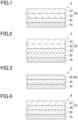
- FIG. 1 an optical film according to a first embodiment of the present invention will be described in detail.
- the optical film 1 includes a colored layer 10, a transparent substrate 20, and a functional layer 30.
- the functional layer 30 includes a low refractive index layer 31 and a hard coat layer 32. That is, the optical film 1 has the transparent substrate 20 located on one surface of the colored layer 10, and is a laminate in which the colored layer 10, the transparent substrate 20, the hard coat layer 32, and the low refractive index layer 31 are laminated in this order.
- the thickness of the optical film 1 may be, for example, preferably in a range of 10 ⁇ m to 140 ⁇ m, more preferably 15 ⁇ m to 120 ⁇ m, and still more preferably 20 ⁇ m to 100 ⁇ m.
- the thickness of the optical film 1 is equal to or greater than the lower limit, the strength of the optical film 1 can be further increased.
- the thickness of the optical film 1 is equal to or less than the upper limit, not only the optical film 1 can be more lightweight but also the display device can be thinner.
- the colored layer 10 is obtained by curing the composition for forming a colored layer of the present invention.
- the composition for forming a colored layer of the present invention contains a dye (A), an ionizing radiation-curable resin (B), a photoinitiator (C), and a solvent (D).
- the composition for forming a colored layer of the present invention may further contain an additive (E).
- the thickness of the colored layer 10 may be, for example, preferably 0.5 ⁇ m to 10 ⁇ m.
- the colored layer 10 can contain a dye to a degree not causing any abnormality in appearance, and the light absorption by the dye improves reflection characteristics and color reproducibility.
- the thickness of the colored layer 10 is equal to or less than the upper limit, it is advantageous in making the display device thinner.
- the thickness of the colored layer 10 is determined by observing the cross section of the optical film 1 in the thickness direction using a microscope or the like.
- the dye (A) in the composition for forming a colored layer according to the above first to eleventh aspects of the present invention contains at least a first colorant and a second colorant.
- the wavelength of maximum absorption of the first colorant is within the range of 470 nm to 530 nm, and the full width at half maximum of the absorption spectrum is 15 nm to 45 nm.
- the wavelength of maximum absorption is lower than the lower limit, the luminance efficiency for blue light emission is likely to decrease, and when it exceeds the upper limit, the luminance efficiency for green light emission is likely to decrease.
- the full width at half maximum of the absorption spectrum is lower than the lower limit, the effect of suppressing external light reflection is reduced.
- the external light reflection characteristics tend to improve but the luminance efficiency is likely to decrease.
- the wavelength of maximum absorption of the second colorant is within the range of 560 nm to 620 nm, and the full width at half maximum of the absorption spectrum is 15 nm to 55 nm.
- the wavelength of maximum absorption is lower than the lower limit, the luminance efficiency for green light emission is likely to decrease, and when it exceeds the upper limit, the luminance efficiency for red light emission is likely to decrease.
- the full width at half maximum of the absorption spectrum is lower than the lower limit, the effect of suppressing external light reflection is reduced.
- the external light reflection characteristics tend to improve but the luminance efficiency is likely to decrease.
- the dye (A) may further contain another colorant other than the first and second colorants.
- the other colorant may be a third colorant.
- the third colorant exhibits the lowest transmittance in the range of 650 nm to 780 nm.
- the wavelength at which the transmittance of the third colorant is lowest within the wavelength range of 380 nm to 780 nm is lower than the lower limit, the luminance efficiency for red light emission is likely to decrease, and when it exceeds the upper limit, the effect of suppressing external light reflection decreases.
- the dye (A) in the composition for forming a colored layer according to the first to eleventh aspects of the present invention includes at least one of the following three types of colorants for selectively absorbing light in the wavelength range of visible light. It may include more than one type of colorant.
- the first colorant has a wavelength of maximum absorption within a first range of 470 nm to 530 nm, and the full width at half maximum of the absorption spectrum is 15 nm to 45 nm.
- the wavelength of maximum absorption is lower than the lower limit, the luminance efficiency for blue light emission is likely to decrease, and when it exceeds the upper limit, the luminance efficiency for green light emission is likely to decrease.
- the full width at half maximum of the absorption spectrum is lower than the lower limit, the effect of suppressing external light reflection is reduced.
- the external light reflection characteristics tend to improve but the luminance efficiency is likely to decrease.
- the second colorant has a wavelength of maximum absorption within a second range of 560 nm to 620 nm, and the full width at half maximum of the absorption spectrum is 15 nm to 55 nm.
- the wavelength of maximum absorption is lower than the lower limit, the luminance efficiency for green light emission is likely to decrease, and when it exceeds the upper limit, the luminance efficiency for red light emission is likely to decrease.
- the full width at half maximum of the absorption spectrum is lower than the lower limit, the effect of suppressing external light reflection is reduced.
- the upper limit the external light reflection characteristics tend to improve but the luminance efficiency is likely to decrease.
- the third colorant exhibits the lowest transmittance in a third range of 650 nm to 780 nm.
- the colored layer 10 has a wavelength of maximum absorption at which the transmittance is 1% or higher and lower than 50% in only one of the first to third ranges.
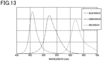
- colorants having the above-described absorption characteristics as the first to third colorants contained in the colored layer 10, it is possible to form a colored layer 10 that absorbs a portion of the visible light emitted by the display device that is in a wavelength range in which the light emission intensity is relatively low.
- the dye (A) preferably contains a compound having a porphyrin structure, merocyanine structure, phthalocyanine structure, azo structure, cyanine structure, squarylium structure, coumarin structure, polyene structure, quinone structure, tetradiporphyrin structure, pyrromethene structure, or indigo structure; or a metal complex thereof.
- a metal complex having a porphyrin structure, pyrromethene structure, or phthalocyanine structure, or a compound having a squarylium structure because of their high reliability.
- the dye (A) may contain only one of these compounds or metal complexes thereof, or two or more of them. These compounds or metal complexes thereof may be contained in the first, second, or third colorant, or in two or more of these colorants.
- the ionizing radiation-curable resin (B) is a resin that is cured by irradiating the resin with ionizing radiation such as ultraviolet light or electron beams for polymerization.
- ionizing radiation such as ultraviolet light or electron beams for polymerization.
- monofunctional, bifunctional, or trifunctional (meth)acrylate monomers or urethane (meth)acrylates, or those with more functional groups can be used, but the ionizing radiation-curable resin (B) of the present invention includes a resin that at least has the ability to scavenge radicals (radical scavenging ability).
- (meth)acrylate” means both or one of "acrylate” and "methacrylate”.
- a resin having radical scavenging ability included in the ionizing radiation-curable resin (B) is a resin having an amine structure.
- the "amine structure” refers to a structure in which the hydrogen atom of ammonia is replaced with a hydrocarbon group or an aromatic group. Examples of the amine structure include primary amine, secondary amine, and tertiary amine. It may also be a quaternary ammonium cation.
- the radical scavenging resin suppresses dye deterioration (fading) by scavenging radicals and suppressing autooxidation when the dye (A) undergoes oxidative deterioration.
- An example of a resin having a radical scavenging amine structure is a resin having a hindered amine structure and a molecular weight of 2,000 or more. When the molecular weight of the resin having a hindered amine structure is 2,000 or more, the effect of suppressing fading can be improved. This is considered to be because many molecules remain in the colored layer 10, and thus a sufficient effect of suppressing fading can be obtained.
- the upper limit of the molecular weight of the resin having a hindered amine structure is not particularly limited, and may be, for example, 50,000.
- molecular weight as used herein means “mass average molecular weight” measured by gel permeation chromatography (GPC) using polystyrene as the standard substance.
- the resin having a radical scavenging amine structure is preferably a polymer with a structural unit represented by the following formula (1).
- R 1 represents a hydrogen atom, halogen atom, carboxyl group, sulfo group, cyano group, hydroxy group, alkyl group having 10 or fewer carbon atoms, alkoxycarbonyl group having 10 or fewer carbon atoms, alkylsulfonylaminocarbonyl group having 10 or fewer carbon atoms, arylsulfonylaminocarbonyl group, alkylsulfonyl group, arylsulfonyl group, acylaminosulfonyl group having 10 or fewer carbon atoms, alkoxy group having 10 or fewer carbon atoms, alkylthio group having 10 or fewer carbon atoms, aryloxy group having 10 or fewer carbon atoms, nitro group, alkoxycarbonyloxy group, aryloxycarbonyloxy group, acyloxy group having 10 or fewer carbon atoms, acyl group having 10 or fewer carbon atoms, carbamo
- R 1 is preferably a hydrogen atom, a hydroxy group, or an alkyl group having 10 or fewer carbon atoms.
- the number of carbon atoms in the alkyl group is preferably 1 to 6, more preferably 1 to 3.
- R 2 is preferably a hydrogen atom or an alkyl group having 10 or fewer carbon atoms.
- the number of carbon atoms in the alkyl group is preferably 1 to 6, more preferably 1 to 3.
- X is preferably a single bond or an aliphatic alkyl chain having 30 or fewer carbon atoms.
- the number of carbon atoms in the aliphatic alkyl chain is preferably 10 or fewer, preferably 1 to 6, more preferably 2 to 4.
- the main component (the component with the highest mass%) of the resin having a radical scavenging amine structure is a copolymer of the structural unit represented by formula (1) and a copolymer component having one of the following repeating units. It becomes possible to control the compatibility with other components by being a copolymer.
- repeating units examples include (meth)acrylate repeating units, olefin repeating units, halogen atom-containing repeating units, styrene repeating units, vinyl acetate repeating units, and vinyl alcohol repeating units.
- Examples of (meth)acrylate repeating units include repeating units derived from (meth)acrylate monomers having a linear or branched alkyl group in their side chains, and repeating units derived from (meth)acrylate monomers having a hydroxyl group in their side chains.
- repeating units derived from (meth)acrylate monomers having a linear or branched alkyl group in their side chains include components derived from monomers such as methyl (meth)acrylate, ethyl (meth)acrylate, propyl (meth)acrylate, isopropyl (meth)acrylate, butyl (meth)acrylate, isobutyl (meth)acrylate, s-butyl (meth)acrylate, t-butyl (meth)acrylate, pentyl (meth)acrylate, hexyl (meth)acrylate, heptyl (meth)acrylate, octyl (meth)acrylate, isooctyl (meth)acrylate, 2-ethylhexyl acrylate, nonyl (meth)acrylate, isononyl (meth)acrylate, decyl (meth)acrylate, isodecyl (meth)acrylate, unde
- repeating units derived from (meth)acrylic monomers having a hydroxyl group in their side chains include components derived from monomers such as 2-hydroxyethyl (meth)acrylate, 2-hydroxypropyl (meth)acrylate, 4-hydroxybutyl (meth)acrylate, 6-hydroxyhexyl (meth)acrylate, and hydroxyphenyl (meth)acrylate. These may be used alone or in combination of two or more.
- olefinic repeating units include components derived from olefinic monomers such as ethylene, propylene, isoprene, and butadiene. These may be used alone or in combination of two or more.
- halogen atom-containing repeating units include components derived from monomers such as vinyl chloride and vinylidene chloride. These may be used alone or in combination of two or more.
- styrene repeating units include components derived from styrene monomers such as styrene, ⁇ -methylstyrene, and vinyltoluene. These may be used alone or in combination of two or more.
- vinyl acetate repeating units examples include esters of saturated carboxylic acids and vinyl alcohol such as vinyl acetate and vinyl propionate. These may be used alone or in combination of two or more.
- vinyl alcohol repeating unit is vinyl alcohol, and it may have a 1,2-glycol bond in its side chain.
- the copolymer may have the structure of a random copolymer, alternating copolymer, block copolymer or graft copolymer.
- the manufacturing process and preparation with other components are easy when the copolymer has the structure of a random copolymer. Therefore, a random copolymer is preferred to the other copolymers.
- Radical polymerization may be used as the polymerization method for obtaining the copolymer. Radical polymerization is preferable because it facilitates industrial production.
- the radical polymerization may be solution polymerization, emulsion polymerization, bulk polymerization, or suspension polymerization.
- the radical polymerization is preferably solution polymerization. By using solution polymerization, the molecular weight of the copolymer can be easily controlled.
- the monomers may be diluted with a polymerization solvent.
- the polymerization solvent may be, for example, an ester solvent, alcohol ether solvent, ketone solvent, aromatic solvent, amide solvent, or alcohol solvent.
- the ester solvent may be, for example, methyl acetate, ethyl acetate, n-butyl acetate, isobutyl acetate, t-butyl acetate, methyl lactate, or ethyl lactate.
- the alcohol ether solvent may be, for example, ethylene glycol monomethyl ether, ethylene glycol monoethyl ether, propylene glycol monomethyl ether, propylene glycol monomethyl ether acetate, propylene glycol monoethyl ether, 3-methoxy-1-butanol, or 3-methoxy-3-methyl-1-butanol.
- the ketone solvent may be, for example, acetone, methyl ethyl ketone, methyl isobutyl ketone, or cyclohexanone.
- the aromatic solvent may be, for example, benzene, toluene, or xylene.
- the amide solvent may be, for example, formamide or dimethylformamide.
- the alcohol solvent may be, for example, methanol, ethanol, n-propanol, isopropanol, n-butanol, isobutanol, s-butanol, t-butanol, diacetone alcohol, or 2-methyl-2-butanol.
- One of the polymerization solvents described above may be used alone or two or more may be mixed together.
- the radical polymerization initiator may be, for example, a peroxide or an azo compound.
- the peroxide may be, for example, benzoyl peroxide, t-butyl peroxyacetate, t-butyl peroxybenzoate, or di-t-butyl peroxide.
- the azo compound may be, for example, azobisisobutyronitrile, an azobisamidinopropane salt, an azobiscyanovaleric acid (salt), or 2,2'-azobis[2-methyl-N-(2-hydroxyethyl) propionamide].
- the content of the structural unit represented by formula (1) is preferably 1 to 100 mol%, more preferably 35 to 100 mol% relative to the total molar quantity of the monomers constituting the ionizing radiation-curable resin (B).
- the content of the structural unit represented by formula (1) is within this range, the lightfastness and heat resistance of the dye (A) are improved, which in turn assists suppressing fading.
- the ionizing radiation-curable resin (B) may further contain a polymer having a structural unit represented by the following formula (2).
- R 3 represents a hydrogen atom, halogen atom, carboxyl group, sulfo group, cyano group, hydroxy group, alkyl group having 10 or fewer carbon atoms, alkoxycarbonyl group having 10 or fewer carbon atoms, alkylsulfonylaminocarbonyl group having 10 or fewer carbon atoms, arylsulfonylaminocarbonyl group, alkylsulfonyl group, arylsulfonyl group, acylaminosulfonyl group having 10 or fewer carbon atoms, alkoxy group having 10 or fewer carbon atoms, alkylthio group having 10 or fewer carbon atoms, aryloxy group having 10 or fewer carbon atoms, nitro group, alkoxycarbonyloxy group, aryloxycarbonyloxy group, acyloxy group having 10 or fewer carbon atoms, acyl group having 10 or fewer carbon atoms, carbamo
- R 3 is preferably a hydrogen atom, a hydroxy group, or an alkyl group having 10 or fewer carbon atoms.
- the number of carbon atoms in the alkyl group is preferably 1 to 6, more preferably 1 to 3.
- R 4 is preferably a hydrogen atom or an alkyl group having 10 or fewer carbon atoms.
- the number of carbon atoms in the alkyl group is preferably 1 to 6, more preferably 1 to 3.
- X is preferably a single bond or an aliphatic alkyl chain having 30 or fewer carbon atoms.
- the number of carbon atoms in the aliphatic alkyl chain is preferably 10 or fewer, preferably 1 to 6, more preferably 2 to 4.
- the polymer having the structural unit represented by formula (2) may be a copolymer with a monomer that is different from the structural unit represented by formula (2). It becomes possible to control the compatibility with other components by being a copolymer.
- the copolymer component may be, for example, a component including one of the above-described (meth)acrylate repeating units, olefin repeating units, halogen atom-containing repeating units, styrene repeating units, vinyl acetate repeating units, and vinyl alcohol repeating units.
- the copolymer may have the structure of a random copolymer, alternating copolymer, block copolymer or graft copolymer.
- the manufacturing process and preparation with other components are easy when the copolymer has the structure of a random copolymer. Therefore, a random copolymer is preferred to the other copolymers.
- Radical polymerization may be used as the polymerization method for obtaining the copolymer. Radical polymerization is preferable because it facilitates industrial production.
- the radical polymerization may be solution polymerization, emulsion polymerization, bulk polymerization, or suspension polymerization.
- the radical polymerization is preferably solution polymerization. By using solution polymerization, the molecular weight of the copolymer can be easily controlled.
- the monomers may be diluted with a polymerization solvent.
- the polymerization solvent may be, for example, an ester solvent, alcohol ether solvent, ketone solvent, aromatic solvent, amide solvent, or alcohol solvent.
- the ester solvent may be, for example, methyl acetate, ethyl acetate, n-butyl acetate, isobutyl acetate, t-butyl acetate, methyl lactate, or ethyl lactate.
- the alcohol ether solvent may be, for example, ethylene glycol monomethyl ether, ethylene glycol monoethyl ether, propylene glycol monomethyl ether, propylene glycol monomethyl ether acetate, propylene glycol monoethyl ether, 3-methoxy-1-butanol, or 3-methoxy-3-methyl-1-butanol.
- the ketone solvent may be, for example, acetone, methyl ethyl ketone, methyl isobutyl ketone, or cyclohexanone.
- the aromatic solvent may be, for example, benzene, toluene, or xylene.
- the amide solvent may be, for example, formamide or dimethylformamide.
- the alcohol solvent may be, for example, methanol, ethanol, n-propanol, isopropanol, n-butanol, isobutanol, s-butanol, t-butanol, diacetone alcohol, or 2-methyl-2-butanol.
- One of the polymerization solvents described above may be used alone or two or more may be mixed together.
- the radical polymerization initiator may be, for example, a peroxide or an azo compound.
- the peroxide may be, for example, benzoyl peroxide, t-butyl peroxyacetate, t-butyl peroxybenzoate, or di-t-butyl peroxide.
- the azo compound may be, for example, azobisisobutyronitrile, an azobisamidinopropane salt, an azobiscyanovaleric acid (salt), or 2,2'-azobis[2-methyl-N-(2-hydroxyethyl) propionamide].
- the amount of the radical polymerization initiator is preferably 0.0001 parts by mass or more and 20 parts by mass or less, more preferably 0.001 parts by mass or more and 15 parts by mass or less, and further preferably 0.005 parts by mass or more and 10 parts by mass or less.
- the radical polymerization initiator may be added to the monomers and the polymerization solvent before initiating polymerization, or may be dropped into the polymerization reaction system. Dropping the radical polymerization initiator into the polymerization reaction system for the monomers and the polymerization solvent is preferable in that the heat generation caused by polymerization can be suppressed.
- the reaction temperature for radical polymerization is selected as appropriate according to the types of radical polymerization initiator and polymerization solvent.
- the reaction temperature is preferably 60°C or higher and 110°C or lower in order to facilitate manufacturing and reaction control.
- the content of the structural unit represented by formula (2) is preferably 1 to 50 mol%, more preferably 1 to 30 mol% relative to the total molar quantity of the monomers constituting the ionizing radiation-curable resin (B).
- the content of the structural unit represented by formula (2) is within this range, the lightfastness and heat resistance of the dye (A) are improved, which in turn assists suppressing fading.
- Examples of the monofunctional (meth)acrylate compound the ionizing radiation-curable resin (B) may contain include 2-hydroxyethyl (meth)acrylate, 2-hydroxypropyl (meth)acrylate, 2-hydroxybutyl (meth)acrylate, n-butyl (meth)acrylate, isobutyl (meth)acrylate, t-butyl (meth)acrylate, glycidyl (meth)acrylate, acryloylmorpholine, N-vinylpyrrolidone, tetrahydrofurfuryl acrylate, cyclohexyl (meth)acrylate, 2-ethylhexyl (meth)acrylate, isobornyl (meth)acrylate, isodecyl (meth)acrylate, lauryl (meth)acrylate, tridecyl (meth)acrylate, cetyl (meth)acrylate, stearyl (meth)acrylate, benzyl (me
- Examples of the bifunctional (meth)acrylate compound the ionizing radiation-curable resin (B) may contain include di(meth)acrylates, such as ethylene glycol di(meth)acrylate, diethylene glycol di(meth)acrylate, butanediol di(meth)acrylate, hexanediol di(meth)acrylate, nonanediol di(meth)acrylate, ethoxylated hexanediol di(meth)acrylate, propoxylated hexanediol di(meth)acrylate, diethylene glycol di(meth)acrylate, polyethylene glycol di(meth)acrylate, tripropylene glycol di(meth)acrylate, polypropylene glycol di(meth)acrylate, neopentyl glycol di(meth)acrylate, ethoxylated neopentyl glycol di(meth)acrylate, tripropylene glycol di(me
- trifunctional (meth)acrylate compound or (meth)acrylate compound having more functional groups that the ionizing radiation-curable resin (B) may contain include tri(meth)acrylates such as trimethylolpropane tri(meth)acrylate, ethoxylated trimethylolpropane tri(meth)acrylate, propoxylated trimethylolpropane tri(meth)acrylate, tris2-hydroxyethylisocyanurate tri(meth)acrylate or glycerin tri(meth)acrylate, trifunctional (meth)acrylate compounds such as pentaerythritol tri(meth)acrylate, dipentaerythritol tri(meth)acrylate or ditrimethylolpropane tri(meth)acrylate, polyfunctional (meth)acrylate compounds having three or more functional groups such as pentaerythritol tetra(meth)acrylate, ditrimethylolpropane tetra(meth)acrylate
- Urethane (meth)acrylate can also be used as the resin that the ionizing radiation-curable resin (B) may contain.
- urethane (meth)acrylate include those obtained by reacting a (meth)acrylate monomer having a hydroxyl group with a product of the reaction between a polyester polyol with an isocyanate monomer or a prepolymer.
- urethane (meth)acrylate examples include a pentaerythritol triacrylate hexamethylene diisocyanate urethane prepolymer, dipentaerythritol pentaacrylate hexamethylene diisocyanate urethane prepolymer, pentaerythritol triacrylate toluene diisocyanate urethane prepolymer, dipentaerythritol pentaacrylate toluene diisocyanate urethane prepolymer, pentaerythritol triacrylate isophorone diisocyanate urethane prepolymer, and dipentaerythritol pentaacrylate isophorone diisocyanate urethane prepolymer.
- the above-listed other monofunctional, bifunctional, or trifunctional (meth)acrylate monomers or urethane (meth)acrylates, those with more functional groups, or the like that the ionizing radiation-curable resin (B) can contain may be used alone or in combination of two or more. It may also be a partially polymerized oligomer.
- the content of the ionizing radiation-curable resin (B) is preferably 20 to 80% by mass, more preferably 30 to 70% by mass relative to the total mass of the composition for forming the colored layer.
- the content of the ionizing radiation-curable resin (B) is equal to or more than the lower limit, the effect of suppressing fading can be further enhanced.
- the content of the ionizing radiation-curable resin (B) is equal to or lower than the upper limit, the composition for forming the colored layer can be handled even easier.
- the photoinitiator (C) when ultraviolet light is used as the ionizing radiation, the photoinitiator (C) generates radicals when ultraviolet light is irradiated.
- photoinitiators (C) include benzoins (including benzoin and benzoin alkyl ethers such as benzoin methyl ether, benzoin ethyl ether, and benzoin isopropyl ether), phenyl ketones [for example, acetophenones (including acetophenone, 2-hydroxy-2-methyl-1-phenylpropane-1-one, 2,2-dimethoxy-2-phenylacetophenone, 2,2-diethoxy-2-phenylacetophenone, and 1,1-dichloroacetophenone), alkylphenyl ketones such as 2-hydroxy-2-methylpropiophenone; and cycloalkylphenyl ketones such as 1-hydroxycyclohexylphenyl ketone], aminoacetophenones ⁇ including 2-methyl-1-[4-(methylthio)phenyl]-2-morpholinoaminopropanone-1,2-benzyl -2-dimethylamino-1-(4-morpholinoph
- the content of the photoinitiator (C) is preferably 0.01 to 20 mass%, more preferably 0.01 to 5 mass% relative to the solid content of the composition for forming the colored layer.
- the content of the photoinitiator (C) is less than the lower limit, the curing effect will be insufficient.
- the content of the photoinitiator (C) exceeds the upper limit, part of the photoinitiator (C) remains unreacted and degrades the reliability of properties such as heat resistance.
- Examples of the solvent (D) include ethers, ketones, esters, and cellosolves.
- Examples of ethers include dibutyl ether, dimethoxymethane, dimethoxyethane, diethoxyethane, propylene oxide, 1,4-dioxane, 1,3-dioxolane, 1,3,5-trioxane, tetrahydrofuran, anisole, and phenetole.
- ketones include acetone, methyl ethyl ketone, diethyl ketone, dipropyl ketone, diisobutyl ketone, methyl isobutyl ketone, cyclopentanone, cyclohexanone, methylcyclohexanone, and ethylcyclohexanone.
- esters include ethyl formate, propyl formate, n-pentyl formate, methyl acetate, ethyl acetate, methyl propionate, ethyl propionate, n-pentyl acetate, and ⁇ -butyrolactone.
- cellosolves examples include methyl cellosolve, cellosolve (ethyl cellosolve), butyl cellosolve, and cellosolve acetate.
- One or a combination of two or more of the solvents (D) may be used.
- the content of the solvent (D) is preferably 20 to 80 mass%, more preferably 30 to 70 mass% relative to the total mass of the composition for forming the colored layer.
- the content of the solvent (D) is equal to or more than the lower limit, the composition for forming the colored layer can be handled even easier.
- the content of the solvent (D) is equal to or lower than the upper limit, the time required to form the colored layer can be reduced.
- the additive (E) may be one or more selected from a radical scavenger, a peroxide decomposer, and a singlet oxygen quencher.
- radical scavengers examples include hindered amine photostabilizers such as 4-isopropylaminodiphenylamine, N-phenyl-1-naphthylamine, and 1,2,2,6,6-pentamethyl-4-piperidyl methacrylate; and phenolic antioxidants such as 2,6-di-t-butyl-p-cresol and 6,6'-di-t-butyl-4,4'-butylidenedi-m-cresol.
- hindered amine photostabilizers such as 4-isopropylaminodiphenylamine, N-phenyl-1-naphthylamine, and 1,2,2,6,6-pentamethyl-4-piperidyl methacrylate
- phenolic antioxidants such as 2,6-di-t-butyl-p-cresol and 6,6'-di-t-butyl-4,4'-butylidenedi-m-cresol.
- peroxide decomposers examples include sulfur-based antioxidants such as ditridecyl-3,3'-thiodipropionate, 2-mercaptobenzothiazole, and 2-mercaptobenzimidazole; and phosphite-based antioxidants such as tris(nonylphenyl)phosphite and 2-ethylhexyl diphenyl phosphite.
- singlet oxygen quenchers include dialkyl phosphates, dialkyldithiocarbanates, benzenedithiols, and transition metal complexes of similar dithiols.
- One or a combination of two or more of the additives (E) may be used.
- additive (E) a leveling agent, antifoaming agent, antioxidant, ultraviolet absorber, photostabilizer, photosensitizer, and conductive material may be used as the additive (E).
- the content of the additive (E) is preferably 0.1 to 20 mass%, more preferably 0.1 to 15 mass% relative to the solid content of the composition for forming the colored layer.
- the content of the additive (E) is less than the lower limit, the effect of suppressing fading is not obtained with regard to the lightfastness and heat resistance of the dye (A).
- the content of the additive (E) exceeds the upper limit, it tends to lead to insufficient curing due to curing inhibition by the additive (E) and/or a decreased amount of the curing component.
- the colored layer 10 improves lightfastness and heat resistance, and in the first to eleventh aspects described above, it is possible to achieve both reflection suppression and luminance efficiency, improve display quality, extend the life of the light emitting elements, and improve color reproducibility.
- the color correction function can be maintained for a long time.
- the transparent substrate 20 is a sheet-like member located on one surface of the colored layer 10 and forming an optical film 1.
- a resin film having translucency may be used as the transparent substrate 20.
- the forming material of the transparent substrate 20 may be a transparent resin or inorganic glass.
- transparent resin include polyolefin, polyester, polyacrylate, polyamide, polyimide, polyarylate, polycarbonate, triacetyl cellulose, polyvinyl alcohol, polyvinyl chloride, cycloolefin copolymer, norbornene-containing resin, polyether sulfone, and polysulfone.
- polyolefins include polyethylene and polypropylene.
- polyesters include polyethylene terephthalate, polybutylene terephthalate, and polyethylene naphthalate.
- An example of polyacrylate is polymethyl methacrylate.
- polyamides include nylon 6 and nylon 66.
- suitable examples are a film of polyethylene terephthalate (PET), a film of triacetyl cellulose (TAC), a film of polymethyl methacrylate (PMMA), and a film of polyester other than PET.
- the thickness of the transparent substrate 20 is not specifically limited, it is preferably in a range of 10 ⁇ m to 100 ⁇ m, for example.
- the transmittance of the transparent substrate 20 is preferably, for example, 90% or higher.
- the transparent substrate 20 may be provided with the ability to absorb ultraviolet light.
- the transparent substrate 20 can be given the ability to absorb ultraviolet light by adding an ultraviolet absorber to the resin material of the transparent substrate 20.
- ultraviolet absorbers examples include salicylic acid ester ultraviolet absorbers, benzophenone ultraviolet absorbers, benzotriazole ultraviolet absorbers, benzotriazine ultraviolet absorbers, and cyanoacrylate ultraviolet absorbers.
- ultraviolet absorbers may be used singly or in combination of two or more.
- the transparent substrate 20 When the transparent substrate 20 is provided with the ability to absorb ultraviolet light, it preferably has an ultraviolet shielding rate of 85% or higher.
- the ultraviolet shielding rate is a value measured in accordance with JIS L 1925, and is calculated by the following formula (I).
- Ultraviolet shielding rate (%) 100 - Average transmittance of ultraviolet light with a wavelength of 290 nm to 400 nm (%)
- An ultraviolet shielding rate below 85% reduces the effect of suppressing fading with regard to the lightfastness of the dye (A).
- Fig. 11 shows the light transmission profiles of polymethyl methacrylate (PMMA), triacetyl cellulose (TAC), and polyethylene terephthalate (PET) that have been given the ability to absorb ultraviolet light.
- PMMA polymethyl methacrylate
- TAC triacetyl cellulose
- PET polyethylene terephthalate
- the ultraviolet shielding rates of the transparent substrates shown by the light transmission profiles in Fig. 11 are as follows. Any of them can be suitably used as the transparent substrate 20 of the present invention.
- the functional layer 30 is located on one or the other surface of the colored layer 10. By having the functional layer 30, the optical film can exhibit various functions.
- Examples of the functions of the functional layer 30 include antireflection function, antiglare function, oxygen barrier function, antistatic function, antifouling function, reinforcement function, and ultraviolet absorption function (ability to absorb ultraviolet light).
- the functional layer 30 may be a monolayer or a multilayer.
- the functional layer 30 may have one function or two or more functions.
- the functional layer 30 functions as an antireflection layer.
- the antireflection layer include a low refractive index layer 31 having a lower refractive index than a hard coat layer 32, an antiglare layer 34, and the transparent substrate 20, which will be described later.
- the low refractive index layer 31 can be formed by using, for the functional layer, a material having a lower refractive index than the materials of the hard coat layer 32, the antiglare layer 34, and the transparent substrate 20.
- fine particles of lithium fluoride (LiF), magnesium fluoride (MgF 2 ), sodium hexafluoroaluminum (cryolite, 3NaF ⁇ AlF 3 , Na 3 AlF 6 ), or aluminum fluoride (AlF 3 ), or fine silica particles may be added. It is effective to use particles having internal voids, such as fine, porous silica particles or hollow silica particles, as the fine silica particles to reduce the refractive index of the low refractive index layer 31.
- the photoinitiator (C), solvent (D), or additive (E) described in relation to the colored layer 10 may be added to the composition for forming the low refractive index layer 31 (composition for forming a low refractive index layer) as appropriate.
- the refractive index of the low refractive index layer 31 is preferably 1.20 to 1.55.
- the thickness of the low refractive index layer 31 is not specifically limited, it is preferably in a range of 40 nm to 1 ⁇ m, for example.
- the functional layer 30 functions as an antiglare layer 34.
- the antiglare layer 34 has small irregularities on its surface so that they scatter external light to suppress reflection and in turn improve display quality.
- the low refractive index layer 31 and the antiglare layer 34 constitute an antireflection layer.
- the antiglare layer 34 contains at least one selected from fine organic particles and fine inorganic particles as necessary.
- the fine organic particles are materials that form small irregularities on the surface and provide the function of scattering external light.
- Examples of fine organic particles include resin particles of translucent resin materials such as acrylic resin, polystyrene resin, styrene-(meth)acrylate copolymers, polyethylene resin, epoxy resin, silicone resin, polyvinylidene fluoride, and polyethylene fluoride resin.
- resin particles of translucent resin materials such as acrylic resin, polystyrene resin, styrene-(meth)acrylate copolymers, polyethylene resin, epoxy resin, silicone resin, polyvinylidene fluoride, and polyethylene fluoride resin.
- two or more types of resin particles having different characteristics may be mixed.
- the fine inorganic particles are a material for controlling sedimentation and aggregation of the fine organic particles.
- Examples of fine inorganic particles include fine silica particles, fine metal oxide particles, and fine particles of various minerals.
- Examples of fine silica particles include colloidal silica, and fine silica particles surface-modified with a reactive functional group such as an (meth)acryloyl group.
- Examples of fine metal oxide particles include fine particles of alumina (aluminum oxide), zinc oxide, tin oxide, antimony oxide, indium oxide, titania (titanium dioxide), and zirconia (zirconium dioxide).
- fine mineral particles examples include fine particles of mica, synthetic mica, vermiculite, montmorillonite, iron-montmorillonite, bentonite, beidellite, saponite, hectorite, stevensite, nontronite, magadiite, ilerite, kanemite, layered titanate, smectite, and synthetic smectite.
- the fine mineral particles may either be natural or synthetic (including substituted products and derivatives), and also a mixture of both may be used.
- organic layered clay is more preferable.
- Organic layered clay refers to a swelling clay in which organic onium ions are introduced between layers.
- the organic onium ion is not particularly limited as long as it can make a swelling clay organic by using the cation exchange properties of the swelling clay.
- the synthetic smectite can be suitably used. Synthetic smectite has a function of increasing the viscosity of the coating liquid for forming the antiglare layer. This suppresses the sedimentation of resin particles and fine inorganic particles and adjusts the shape of the irregularities on the surface of the antiglare layer 34 (functional layer 30).
- the functional layer 30 functions as an oxygen barrier layer 33.
- the oxygen barrier layer 33 has an oxygen permeability of 10 cm 3 /(m 2 ⁇ day ⁇ atm) or lower, preferably 5 cm 3 /(m 2 ⁇ day ⁇ atm) or lower, and more preferably 1 cm 3 /(m 2 ⁇ day ⁇ atm) or lower.
- the oxygen permeability of the oxygen barrier layer 33 is equal to or lower than the upper limit, the functional layer 30 can be provided with a sufficient oxygen barrier function.
- the lower limit of the oxygen permeability of the oxygen barrier layer 33 is not particularly limited, and may be 0 cm 3 /(m 2 ⁇ day ⁇ atm).
- the oxygen permeability of the oxygen barrier layer 33 is a value measured using an oxygen permeability measuring device at 30°C and a relative humidity of 60%.
- the functional layer 30 functions as an antistatic layer.
- the antistatic layer include layers containing antistatic agents such as fine metal oxide particles such as antimony-doped tin oxide (ATO) and tin-doped indium oxide (ITO), polymeric conductive compositions, and quaternary ammonium salts.
- the antistatic layer may be provided on the outermost surface of the functional layer 30 or between the functional layer 30 and the transparent substrate 20.
- the antistatic layer may be formed by adding an antistatic agent to one of the above-described layers constituting the functional layer 30.
- the optical film preferably has a surface resistance of 1.0 ⁇ 10 6 to 1.0 ⁇ 10 12 ( ⁇ /cm).
- the functional layer 30 functions as an antifouling layer.
- the antifouling layer improves the antifouling performance by imparting both or one of water repellency and oil repellency.
- Examples of the antifouling layer include layers containing antifouling agents such as silicon oxide, fluorine-containing silane compounds, fluoroalkylsilazane, fluoroalkylsilane, fluorine-containing silicon compounds, and perfluoropolyether group-containing silane coupling agents.
- the antifouling layer may be provided on the outermost surface of the functional layer 30, or formed by adding an antifouling agent to the outermost layer of the functional layer(s) 30.
- the functional layer 30 functions as a reinforcement layer.
- the reinforcement layer is a layer that reinforces the optical film.
- An example of the reinforcement layer is the hard coat layer 32.
- the hard coat layer 32 include layers formed with a hard coat agent containing monofunctional, bifunctional, or trifunctional (meth)acrylate or urethane (meth)acrylate, or (meth)acrylate or urethane (meth)acrylate with more functional groups.
- the functional layer 30 functions as an ultraviolet absorbing layer.
- the ultraviolet absorbing layer include layers containing triazine ultraviolet absorbers such as 2-(4,6-diphenyl-1,3,5-triazin-2-yl)-5-hexyloxyphenol and benzotriazole ultraviolet absorbers such as 2-(2H-benzotriazole-2-yl)-4-methylphenol.
- the content of the ultraviolet absorber is preferably 0.1 to 5 mass% relative to the total mass of the materials forming the ultraviolet absorbing layer.
- the functional layer 30 can be provided with sufficient ultraviolet absorbance.
- the content of the ultraviolet absorber is equal to or lower than the upper limit, it is possible to avoid insufficient hardness due to a decrease in the amount of the curing component.
- one or both of the transparent substrate 20 and the functional layer 30 have an ultraviolet shielding rate of 85% or higher, preferably 90% or higher, more preferably 95% or higher. It may even be 100%.
- the ultraviolet shielding rate is equal to or higher than the lower limit, lightfastness and heat resistance can be further improved.
- the ultraviolet shielding rate can be measured according to the method described in JIS L 1925.
- the ultraviolet shielding rate can be adjusted by imparting ultraviolet absorbing ability to one or both of the transparent substrate 20 and the functional layer 30.
- the thickness of the functional layer 30 may be, for example, preferably in a range of 0.04 ⁇ m to 25 ⁇ m, more preferably 0.1 ⁇ m to 20 ⁇ m, and still more preferably 0.2 ⁇ m to 15 ⁇ m.
- the thickness of the functional layer 30 is equal to or greater than the lower limit, it becomes easier to impart various functions to the optical film 1.
- the thickness of the functional layer 30 is equal to or less than the upper limit, it is advantageous in making the display device thinner.
- the optical film 1 of this embodiment can be manufactured by a conventionally known method.
- the colored layer 10 is obtained by applying a composition for forming the colored layer to one surface of the transparent substrate 20 and curing the composition by irradiating it with ionizing radiation.
- the light source for irradiating the composition for forming the colored layer with ionizing radiation to cure it and form the colored layer 10 can be any light source that generates ionizing radiation.
- the ionizing radiation include optical energy radiation such as radiation (such as gamma rays and X-rays), ultraviolet light, visible light, and electron beams (EB). Usually ultraviolet light and electron beams are used.
- lamps emitting ultraviolet light include low-pressure mercury vapor lamps, medium-pressure mercury vapor lamps, high-pressure mercury vapor lamps, carbon arc lamps, metal halide lamps, xenon lamps, and electrodeless lamps.
- the ultraviolet light is usually irradiated at 100 to 1000 mJ/cm 2 .
- a hard coat agent is applied to the other surface of the transparent substrate 20.
- the applied hard coat agent is irradiated with ionizing radiation to cure it, thereby obtaining the hard coat layer 32.
- an optical film 1 having the functional layer 30 on the other surface of the transparent substrate 20 can be obtained.
- the method of forming the low refractive index layer 31 is not particularly limited.
- it may be formed by applying a composition for forming a low refractive index layer to the hard coat layer 32 and irradiating the applied composition with ionizing radiation to cure it, vacuum evaporation, sputtering, ion plating, an ion beam method, or plasma-enhanced chemical vapor deposition.
- the optical film may be an optical film 2 in which the transparent substrate 20 is located on one surface of the colored layer 10, and the colored layer 10, the transparent substrate 20, the oxygen barrier layer 33, the hard coat layer 32, and the low refractive index layer 31 are laminated in this order.
- the oxygen barrier layer 33, the hard coat layer 32, and the low refractive index layer 31 constitute the functional layer 30.
- optical film 2 of this embodiment has the oxygen barrier layer 33, it exhibits better oxygen barrier performance than the optical film 1.
- the optical film may be an optical film 3 in which the transparent substrate 20 is located on one surface of the colored layer 10, and the colored layer 10, the transparent substrate 20, and the antiglare layer 34 are laminated in this order.
- the antiglare layer 34 forms the functional layer 30.
- the optical film 3 of this embodiment has the antiglare layer 34, it suppresses reflection well.
- the optical film may be an optical film 4 in which the transparent substrate 20 is located on one surface of the colored layer 10, and the colored layer 10, the transparent substrate 20, the antiglare layer 34, and the low refractive index layer 31 are laminated in this order.
- the antiglare layer 34 and the low refractive index layer 31 constitute the functional layer 30.
- the optical film 4 of this embodiment has the low refractive index layer 31 and the antiglare layer 34, it suppresses reflection even better.
- the optical film may be an optical film 5 in which the transparent substrate 20 is located on one surface of the colored layer 10, and the functional layer 30 is located on the other surface of the colored layer 10.
- the transparent substrate 20, the colored layer 10, the hard coat layer 32, and the low refractive index layer 31 are laminated in this order.
- the hard coat layer 32 and the low refractive index layer 31 constitute the functional layer 30.
- the optical film 5 of this embodiment has the colored layer 10 and the functional layer 30 having an ultraviolet absorbing function and an antireflection function on one surface of the transparent substrate 20.
- the optical film may be an optical film 6 in which the transparent substrate 20 is located on one surface of the colored layer 10, and the functional layer 30 is located on the other surface of the colored layer 10.
- the transparent substrate 20, the colored layer 10, the oxygen barrier layer 33, the hard coat layer 32, and the low refractive index layer 31 are laminated in this order.
- the oxygen barrier layer 33, the hard coat layer 32, and the low refractive index layer 31 constitute the functional layer 30.
- the optical film 6 of this embodiment has the oxygen barrier layer 33, it exhibits good oxygen barrier performance.
- the optical film may be an optical film 7 in which the transparent substrate 20 is located on one surface of the colored layer 10, and the functional layer 30 is located on the other surface of the colored layer 10.
- the transparent substrate 20, the colored layer 10, and the antiglare layer 34 are laminated in this order.
- the antiglare layer 34 forms the functional layer 30.
- optical film 7 of this embodiment has the antiglare layer 34, it suppresses reflection well.
- the optical film may be an optical film 8 in which the transparent substrate 20 is located on one surface of the colored layer 10, and the functional layer 30 is located on the other surface of the colored layer 10.
- the transparent substrate 20, the colored layer 10, the antiglare layer 34, and the low refractive index layer 31 are laminated in this order.
- the antiglare layer 34 and the low refractive index layer 31 constitute the functional layer 30.
- the optical film 8 of this embodiment has the low refractive index layer 31 and the antiglare layer 34, it suppresses reflection even better.
- the display device of the present invention has the optical film of the present invention.
- Specific examples of the display device include television, monitors, mobile phones, portable game machines, portable information terminals, personal computers, electronic books, video cameras, digital still cameras, head mounted displays, navigation systems, sound reproduction devices (car audio systems, digital audio players, and the like), copiers, facsimiles, printers, multifunction printers, vending machines, automated teller machines (ATM), personal identification devices, optical communication devices, and IC cards.
- display devices having self-emissive elements such as LEDs, organic EL, inorganic phosphor, and quantum dots that are susceptible to external light reflection due to having metal electrodes and wiring.
- the optical film of this embodiment since it has a colored layer containing the composition for forming a colored layer of the present invention, lightfastness and heat resistance can be improved, and therefore reflection suppression and luminance efficiency can both be achieved. This allows a display device including the optical film of this embodiment to improve display quality and extend the life of the light-emitting elements.
- the reflectiveness of the display device decreases significantly.
- the transmittance is halved when a circularly polarizing plate is used, a high white display transmittance, good luminance efficiency, and improved color reproducibility are provided. This makes it possible to achieve both improved display characteristics and reliability.
- a display device to which the optical film of this embodiment is applied has a good balance between white display performance and color reproducibility. Since it is also highly reliable, it can withstand long-term use.
- the optical film of this embodiment has one colored layer 10, there may be two or more colored layers.
- the ultraviolet absorbing ability may be imparted to the transparent substrate 20 or to the functional layer 30 such as the hard coat layer 32.
- optical films A to M having the layer structures shown in Tables 1 and 2 were prepared. Simulations were performed using the prepared optical films A to M to evaluate their optical film characteristics, and display device characteristics when applied to an organic EL panel. In the tables, "-" means that the layer was not provided. [Table 1] Ex. 1 Ex. 2 Ex. 3 Ex. 4 Ex. 5 Ex. 6 Ex. 7 Ex.
- the following materials were used for the composition for forming the colored layer.
- the wavelength of maximum absorption, the full width at half maximum, and the wavelength of minimum transmittance in a specified wavelength range of a colorant are its characteristic values in the state of a cured coating film.
- Dye-1 Pyrromethene cobalt complex dye represented by the following formula (3) (with a wavelength of maximum absorption of 493 nm, a full width at half maximum of 26 nm).
- Dye-2 Tetraazaporphyrin copper complex dye (PD-311S manufactured by Yamamoto Chemicals Inc., with a wavelength of maximum absorption of 586 nm and a full width at half maximum of 22 nm).
- Dye-3 Tetraazaporphyrin copper complex dye (FDG-007 manufactured by Yamada Chemical Co., Ltd., with a wavelength of maximum absorption of 595 nm and a full width at half maximum of 22 nm).
- Dye-4 Phthalocyanine copper complex dye (FDN-002 manufactured by Yamada Chemical Co., Ltd., with a wavelength of minimum transmittance of 780 nm within 380 to 780 nm).
- the initiator 2,2'-azobis(isobutyronitrile) can be completely decomposed. This suppresses deterioration of the optical film due to the remaining initiator.
- compositions for forming colored layers shown in Table 3 were applied onto the transparent substrates shown in Tables 1 and 2, and dried in an oven at 80°C for 60 seconds. After that, the coating film was cured by irradiating it with ultraviolet light at an irradiation dose of 150 mJ/cm 2 using an ultraviolet irradiation device (a light source, H-bulb, manufactured by Fusion UV Systems Japan) so that a colored layer having a film thickness of 5.0 ⁇ m after curing is formed. Note that the amount added is expressed in mass ratio (mass%). In the tables, "-" means that the component is not present.
- the above composition for forming an oxygen barrier layer was applied to the transparent substrate of Example 7 shown in Table 1, and dried to form an oxygen barrier layer having an oxygen permeability of 1 cm 3 /(m 2 ⁇ day ⁇ atm).
- the following materials were used for the composition for forming the hard coat layer.
- UA-306H Pentaerythritol triacrylate hexamethylene diisocyanate urethane prepolymer (UA-306H manufactured by Kyoeisha Chemical Co., Ltd.).
- DPHA Dipentaerythritol hexaacrylate.
- PETA Pentaerythritol triacrylate.
- Omnirad TPO An acyl phosphine oxide photoinitiator (manufactured by IGM Resins B.V.).
- UV absorber Ultraviolet (UV) absorber
- Tinuvin 479 A hydroxyphenyltriazine ultraviolet absorber, Tinuvin (registered trademark) 479 (manufactured by BASF Japan Ltd.).
- LA-36 A benzotriazole ultraviolet absorber, ADK STAB (registered trademark) LA-36 (manufactured by ADEKA CORPORATION).
- compositions for forming hard coat layers shown in Table 4 were applied onto the transparent substrates or oxygen barrier layers shown in Tables 1 and 2, and dried in an oven at 80°C for 60 seconds. After that, the coating film was cured by irradiating it with ultraviolet light at an irradiation dose of 150 mJ/cm 2 using an ultraviolet irradiation device (a light source, H-bulb, manufactured by Fusion UV Systems Japan) so that a hard coat layer having a film thickness of 5.0 ⁇ m after curing is formed. Note that the amount added is expressed in mass ratio (mass%). In the tables, "-" means that the component is not present.
- Hard coat layer 1 Hard coat layer125 Ionizing radiation-curable resin Type UA-3 06H/DPHA/PETA Ratio 70/20/10 Amount added 45.4% 42.2% Photoinitiator Type Omnirad TPO Amount added 4.6% UV absorber Type - Tinuvin 479/LA-36 Ratio - 40/60 Amount added - 3.2% Solvent Type MEK/Methyl acetate Ratio 50/50 Amount added 50%
- the following materials were used for the composition for forming the antiglare layer.
- Omnirad TPO manufactured by IGM Resins B.V. 4.55 parts by mass.
- Styrene-methyl methacrylate copolymer particles (refractive index 1.515, average particle size 2.0 ⁇ m) 0.5 part by mass.
- Alumina nanoparticles (average particle size 40 nm) 1.0 parts by mass.
- the above composition for forming an antiglare layer was applied onto a transparent substrate shown in Table 1, and dried in an oven at 80°C for 60 seconds. After that, the coating film was cured by irradiating it with ultraviolet light at an irradiation dose of 150 mJ/cm 2 using an ultraviolet irradiation device (a light source, H-bulb, manufactured by Fusion UV Systems Japan) so that an antiglare layer having a film thickness of 5.0 ⁇ m after curing is formed.
- an ultraviolet irradiation device a light source, H-bulb, manufactured by Fusion UV Systems Japan
- composition for forming the low refractive index layer (Composition for forming the low refractive index layer)
- the following materials were used for the composition for forming the low refractive index layer.
- Optool registered trademark
- AR-110 manufactured by Daikin Industries, Ltd., solid content 15%, solvent: methyl isobutyl ketone
- Pentaerythritol triacrylate (PETA) 0.4 parts by mass.
- Omnirad TPO manufactured by IGM Resins B.V. 0.07 parts by mass.
- Methyl ethyl ketone 83.73 parts by mass.
- the above composition for forming the low refractive index layer was applied onto the hard coat layers or oxygen barrier layers shown in Tables 1 and 2, and dried in an oven at 80°C for 60 seconds. After that, the coating film was cured by irradiating it with ultraviolet light at an irradiation dose of 200 mJ/cm 2 using an ultraviolet irradiation device (a light source, H-bulb, manufactured by Fusion UV Systems Japan) so that a low refractive index layer having a film thickness of 100 nm after curing is formed.
- an ultraviolet irradiation device a light source, H-bulb, manufactured by Fusion UV Systems Japan
- the transmittance was measured using an automatic spectrophotometer (U-4100 manufactured by Hitachi, Ltd.).
- U-4100 manufactured by Hitachi, Ltd.
- the layers above the colored layer were peeled off using a transparent pressure-sensitive adhesive tape that satisfies the JIS-K5600-5-6:1999 adhesion test. Then, using an adhesive tape as a reference, the transmittance of the layers above the colored layer was measured with the automatic spectrophotometer (U-4100 manufactured by Hitachi, Ltd.).
- the films were tested using a xenon weather meter testing machine (X75 manufactured by Suga Test Instruments Co., Ltd.) for 120 hours with a xenon lamp illuminance of 60 W/m 2 (300 nm to 400 nm) and at a temperature of 45°C and humidity (RH) of 50% inside the testing machine.
- X75 manufactured by Suga Test Instruments Co., Ltd.
- the transmittance was measured before and after the test to calculate a transmittance difference ⁇ T ⁇ 1 between before and after the test at a wavelength ⁇ 1 at which the minimum transmittance is obtained before the test within the wavelength range of 470 nm to 530 nm, as well as a transmittance difference ⁇ T ⁇ 2 between before and after the test at a wavelength ⁇ 2 at which the minimum transmittance is obtained before the test within the wavelength range of 560 nm to 620 nm.
- ⁇ 20 (N 1 to 3), more preferably
- ⁇ 10 (N 1 to 3).
- the films were tested for 500 hours at a temperature of 90°C.
- the transmittance was measured before and after the test to calculate a transmittance difference ⁇ T ⁇ 1 between before and after the test at a wavelength ⁇ 1 at which the minimum transmittance is obtained before the test within the wavelength range of 470 nm to 530 nm, as well as a transmittance difference ⁇ T ⁇ 2 between before and after the test at a wavelength ⁇ 2 at which the minimum transmittance is obtained before the test within the wavelength range of 560 nm to 620 nm.
- ⁇ 20 (N 1 to 3), more preferably
- ⁇ 10 (N 1 to 3).
- the transmittance of the obtained optical films was measured with the automatic spectrophotometer (U-4100 manufactured by Hitachi, Ltd.). Using this transmittance, the efficiency of light transmitted through the optical film during the white display was calculated and used as an evaluation of the white display transmission properties.
- the efficiency of the spectrum during the white display output from a white organic EL light source and through a color filter having the spectrum shown in Fig. 9 was set as 100. The closer it is to 100, the higher the white display transmittance and the better the luminance efficiency.
- the transmittance T ( ⁇ ) and surface reflectance R ( ⁇ ) were measured for each of the obtained optical films using the automatic spectrophotometer (U-4100 manufactured by Hitachi, Ltd.).
- U-4100 manufactured by Hitachi, Ltd.
- a matte black dye was applied to the surface of the functional layer opposite to its outermost surface to prevent reflection, and the spectral reflectance was measured at an incident angle of 5° and used as the surface reflectance R( ⁇ ).
- the relative reflection was calculated based on the following formula (II).
- the calculated relative reflectance was used as an evaluation of the display device reflection properties. The lower the value of the display device reflection properties, the more the reflection of external light can be reduced and the better the reflection properties.
- R( ⁇ ) represents the surface reflectance of the outermost layer on the observer side
- T( ⁇ ) represents the transmittance of the optical film
- P( ⁇ ) represents the spectrum of the D65 light source
- y( ⁇ ) represents a CIE 1931 color matching function.
- the transmittance of the obtained optical films was measured using the automatic spectrophotometer (U-4100 manufactured by Hitachi, Ltd.), and the red display, green display, and blue display spectra of Fig. 10 output from the white EL light source and through the color filter having the spectrum shown in Fig. 9 was measured.
- the vertical axis of the graphs in Figs. 9 and 10 indicates emission intensity [arbitrary unit (a. u.)].
- the National Television Broadcast Standards Committee (NTSC) ratio was calculated from the CIE 1931 chromaticity value calculated using the measured transmittance and the red display, green display, and blue display spectra in Fig. 10 .
- the NTSC ratio was evaluated as a metric of the color reproducibility. The higher the NTSC ratio, the better the color reproducibility.
- optical films (Examples 1 to 8) having a colored layer formed using the composition for forming the colored layer including the dye (A), ionizing radiation-curable resin (B), photoinitiator (C), and solvent (D) according to the present invention have good lightfastness and heat resistance.
- the optical films (Examples 3 to 8) having a colored layer of a composition for colored layer formation further containing a singlet oxygen quencher as an additive (E) have even better lightfastness.
- the reflection properties of the display devices having the colored layers according to the present invention decreased significantly (Examples 1 to 8).
- the transmittance is halved when a circularly polarizing plate is used, it was confirmed that a high white display transmittance properties, good luminance efficiency, and improved color reproducibility are provided. This makes it possible to achieve both improved display characteristics and reliability.
- optical films A to T having the layered configurations shown in Tables 7 and 8 were prepared. Simulations were performed to evaluate the characteristics of the prepared films and their display device characteristics when used with an organic EL panel. In the tables, "-" means that the layer was not provided. [Table 7] Ex. 1B Ex. 2B Ex. 3B Ex. 4B Ex. 5B Ex. 6B Ex. 7B Ex. 8B Ex. 9B Ex. 10B Ex.
- the following substrate was used as the substrate.
- the following materials were used for the composition for forming the colored layer.
- the wavelength of maximum absorption, the full width at half maximum, and the wavelength of minimum transmittance in a specified wavelength range of a colorant are its characteristic values in the state of a cured coating film.
- Dye-1 Pyrromethene cobalt complex dye (with a wavelength of maximum absorption of 493 nm and a full width at half maximum of 26 nm)
- Dye-4 Phthalocyanine copper complex dye (FDN-002 manufactured by Yamada Chemical Co., Ltd., with a wavelength of minimum transmittance of 780 nm within 380 to 780 nm)
- the initiator 2,2'-azobis(isobutyronitrile) can be completely decomposed. This suppresses deterioration of the optical film due to the remaining initiator.
- Methyl ethyl ketone and methyl acetate were mixed as appropriate and used.
- compositions for forming colored layers shown in Table 9 were each applied onto one surface of a substrate, and dried in an oven at 80°C for 60 seconds. After that, the coating film was cured by irradiating it with ultraviolet light at an irradiation dose of 150 mJ/cm 2 using an ultraviolet irradiation device (a light source, H-bulb, manufactured by Fusion UV Systems Japan) to form colored layers 1 to 15. Note that the amount added is expressed in mass ratio (mass%). In the tables, "-" means that the component is not present.
- the above composition for forming an oxygen barrier layer was applied to the transparent substrate of Example 9B shown in Table 7, and dried to form an oxygen barrier layer having an oxygen permeability of 1 cm 3 /(m 2 ⁇ day ⁇ atm).
- the following materials were used for the composition for forming the hard coat layer.
- UA-306H Pentaerythritol triacrylate hexamethylene diisocyanate urethane prepolymer (UA-306H manufactured by Kyoeisha Chemical Co., Ltd.).
- DPHA Dipentaerythritol hexaacrylate.
- PETA Pentaerythritol triacrylate.
- Omnirad TPO An acyl phosphine oxide photoinitiator (manufactured by IGM Resins B.V.).
- UV absorber Ultraviolet (UV) absorber
- Tinuvin 479 A hydroxyphenyltriazine ultraviolet absorber, Tinuvin (registered trademark) 479 (manufactured by BASF Japan Ltd.).
- LA-36 A benzotriazole ultraviolet absorber, ADK STAB (registered trademark) LA-36 (manufactured by ADEKA CORPORATION).
- compositions for forming hard coat layers shown in Table 10 were applied onto the transparent substrates, oxygen barrier layer, or colored layers shown in Tables 7 and 8, and dried in an oven at 80°C for 60 seconds. After that, the coating film was cured by irradiating it with ultraviolet light at an irradiation dose of 150 mJ/cm 2 using an ultraviolet irradiation device (a light source, H-bulb, manufactured by Fusion UV Systems Japan) so that a hard coat layer having a film thickness of 5.0 ⁇ m after curing is formed. Note that the amount added is expressed in mass ratio (mass%). In the tables, "-" means that the component is not present.
- Hard coat layer 1 Hard coat layer 2 Ionizing radiation-curable resin (B) Type UA-306H/DPHA/PETA Ratio 70/20/10 Amount added 45.4% 42.2% Photoinitiator Type Omnirad TPO Amount added 4.6% UV absorber Type - Tinuvin 479/LA36 Ratio - 40/60 Amount added - 3.2% Solvent Type MEK/Methyl acetate Ratio 50/50 Amount added 50%
- composition for forming antiglare layer Composition for forming antiglare layer
- the following materials were used for the composition for forming the antiglare layer.
- Omnirad TPO manufactured by IGM Resins B.V. 4.55 parts by mass.
- Styrene-methyl methacrylate copolymer particles (refractive index 1.515, average particle size 2.0 ⁇ m) 0.5 part by mass.
- Alumina nanoparticles (average particle size 40 nm) 1.0 parts by mass.
- the above composition for forming an antiglare layer was applied onto a transparent substrate shown in Table 7, and dried in an oven at 80°C for 60 seconds. After that, the coating film was cured by irradiating it with ultraviolet light at an irradiation dose of 150 mJ/cm 2 using an ultraviolet irradiation device (a light source, H-bulb, manufactured by Fusion UV Systems Japan) so that an antiglare layer having a film thickness of 5.0 ⁇ m after curing is formed.
- an ultraviolet irradiation device a light source, H-bulb, manufactured by Fusion UV Systems Japan
- composition for forming the low refractive index layer (Composition for forming the low refractive index layer)
- the following materials were used for the composition for forming the low refractive index layer.
- the above composition for forming the low refractive index layer was applied to the hard coat layers or antiglare layers shown in Tables 7 and 8, and dried in an oven at 80°C for 60 seconds. After that, each of the coating films was cured by irradiating it with ultraviolet light at an irradiation dose of 200 mJ/cm 2 using an ultraviolet irradiation device (a light source, H-bulb, manufactured by Fusion UV Systems Japan) so that a low refractive index layer having a film thickness of 100 nm after curing is formed.
- an ultraviolet irradiation device a light source, H-bulb, manufactured by Fusion UV Systems Japan
- the transmittance was measured using an automatic spectrophotometer (U-4100 manufactured by Hitachi, Ltd.).
- U-4100 manufactured by Hitachi, Ltd.
- the layers above the colored layer were peeled off using a transparent pressure-sensitive adhesive tape that satisfies the JIS-K5600-5-6:1999 adhesion test. Then, using an adhesive tape as a reference, the transmittance of the layers above the colored layer was measured with the automatic spectrophotometer (U-4100 manufactured by Hitachi, Ltd.).
- the films were tested using a xenon weather meter testing machine (X75 manufactured by Suga Test Instruments Co., Ltd.) for 120 hours with a xenon lamp illuminance of 60 W/cm 2 (300 to 400 nm) and at a temperature of 45°C and humidity (RH) of 50% inside the testing machine.
- a xenon weather meter testing machine X75 manufactured by Suga Test Instruments Co., Ltd.
- the transmittance was measured before and after the test to calculate, for each of the first to third ranges described above, a transmittance difference ⁇ T between before and after the test at a wavelength ⁇ at which the minimum transmittance was obtained before the test within the corresponding one of the first to third ranges. The closer the transmittance difference is to zero, the better.
- Each of the optical film samples was stored at 90° C for 500 hours.
- the transmittance was measured before and after the storage to calculate, for each of the first to third ranges described above, a transmittance difference ⁇ T between before and after the test at a wavelength ⁇ at which the minimum transmittance was obtained before the test within that range. The closer the transmittance difference is to zero, the better.
- Simulations were performed as follows to evaluate the characteristics of display devices provided with the obtained optical films C, F, G, and Q to T.
- the display devices had a configuration in which the optical film is bonded to an organic EL display device (target object).
- the organic EL display device which is the target object to which the optical film is bonded, has a spectrum as shown in Fig. 12 during the white display, and individual spectra as shown in Fig. 13 during the red, green, and blue displays.
- the transmittance of each of the obtained optical films was measured using the automatic spectrophotometer (U-4100 manufactured by Hitachi, Ltd.). This transmittance of the optical film was multiplied by the individual spectrum during the white display of the EL display device without the optical film (see Fig. 12 ) to calculate the spectrum after passing through the optical film. After multiplying each of the individual spectrum of the organic EL display device during the white display and the spectrum after passing through the optical film by the luminous efficiency to calculate their Y values, the ratio between the Y values was determined assuming that the Y value obtained from the individual spectrum during the white display of the organic EL display device is 100. The determined ratio was assumed as the efficiency and used as a metric of the transmission properties of the display device.
- the transmittance of each of the obtained optical films was measured using the automatic spectrophotometer (U-4100 manufactured by Hitachi, Ltd.). Each of the individual spectra in the red, green, and blue displays of the organic EL display device without the optical film (see Fig. 13 ) was multiplied by this transmittance of the optical film to calculate the chromaticity (x, y) for each of monochromatic red, green, and blue in the Commission International de l'Eclairage (CIE) 1931 color space after passing through the optical film.
- CIE Commission International de l'Eclairage
- the optical films (Examples 1B to 10B) having a colored layer formed using the composition for forming the colored layer including the dye (A), ionizing radiation-curable resin (B), photoinitiator (C), and solvent (D) according to the present invention have good lightfastness and heat resistance.
- the optical films having a colored layer of a composition for colored layer formation further containing a singlet oxygen quencher as an additive (E) have even better lightfastness.
- a transparent substrate or a functional layer having an ultraviolet absorbing ability that provides an ultraviolet shielding rate of 85% or higher was provided on the colored layer of the optical film, the lightfastness improved significantly as compared with when the colored layer did not have the ultraviolet absorbing ability.
- an oxygen barrier layer was provided on the colored layer of the present invention, the lightfastness was further improved.
- the antiglare layer may be provided with ultraviolet absorbing ability to further enhance lightfastness.
- the antifouling layer may be included in the functional layer.
- the antifouling layer can improve the antifouling performance by imparting one or both of water repellency and oil repellency.
- Examples of the antifouling layer include layers containing antifouling agents such as silicon oxide, fluorine-containing silane compounds, fluoroalkylsilazane, fluoroalkylsilane, fluorine-containing silicon compounds, and perfluoropolyether group-containing silane coupling agents.
- the antifouling layer may be provided on the outermost surface of the functional layer, or an antifouling agent may be added to the outermost layer of the functional layer(s) so that it functions as the antifouling layer.
- the antistatic layer may be included in the functional layer.
- the antistatic layer include layers containing antistatic agents such as fine metal oxide particles such as antimony-doped tin oxide (ATO) and tin-doped indium oxide (ITO), polymeric conductive compositions, and quaternary ammonium salts.
- the antistatic layer may be provided on the outermost surface of the functional layer or between the functional layer and the transparent substrate.
- an antistatic agent may be added to one of the above-described layers constituting the functional layer so that it functions as the antistatic layer.
- the optical film preferably has a surface resistance of 1.0 ⁇ 10 6 to 1.0 ⁇ 10 12 ( ⁇ /cm).
- a composition for forming a colored layer, an optical film, and a display device capable of improving lightfastness and heat resistance, achieving both reflection suppression and luminance efficiency, improving display quality, extending the life of the light emitting elements, and improving color reproducibility can be provided.
- the present invention can be applied to an optical film used in a display device.
Landscapes
- Chemical & Material Sciences (AREA)
- Organic Chemistry (AREA)
- Health & Medical Sciences (AREA)
- Chemical Kinetics & Catalysis (AREA)
- Medicinal Chemistry (AREA)
- Polymers & Plastics (AREA)
- Physics & Mathematics (AREA)
- Engineering & Computer Science (AREA)
- General Physics & Mathematics (AREA)
- Optics & Photonics (AREA)
- Life Sciences & Earth Sciences (AREA)
- Materials Engineering (AREA)
- Wood Science & Technology (AREA)
- Inorganic Chemistry (AREA)
- Theoretical Computer Science (AREA)
- Compositions Of Macromolecular Compounds (AREA)
- Polymerisation Methods In General (AREA)
- Liquid Crystal (AREA)
Abstract
Description
- The present invention relates to a composition for forming a colored layer, an optical film and a display device.
- The present application claims priority to
Japanese Patent Application No. 2021-132535 filed on August 17, 2021 Japanese Patent Application No. 2022-004645 filed on January 14, 2022 Japanese Patent Application No. 2022-004646 filed on January 14, 2022 - Display devices are often used in environments where there is incident external light, whether indoors or outdoors. The external light incident on the display device is reflected at the surface of the display device, causing a reduction in display quality. In particular, self-emissive display devices such as organic light emitting display devices have the problem that the electrodes and many other metal wirings strongly reflect external light, which tends to degrade display quality. However, they are expected to provide next-generation display devices due to their high quality characteristics such as the ability to reduce size, low power consumption, high luminance, and high response speed.
- Configurations are known in which a polarizing plate and a retarder are placed on the display surface side to suppress reflection of external light and thereby solve the problem of drop in display quality due to reflection of external light.
- However, in the method using a polarizing plate and a retarder, when light from the display device passes through the polarizing plate and retarder and is emitted externally, a considerable portion of the light is lost. This tends to reduce the lifespan of the device.
- In addition, display devices are generally required to have high color purity. Color purity indicates the range of colors a display device can display, and is also called color reproduction range. Therefore, high color purity means a wide color reproduction range and good color reproducibility. Known means of improving color reproducibility include a method in which a color filter for separating colors is applied to a light source that emits white light, and a method in which a color filter for correction is applied to light sources that emit monochromatic light of the three primary colors RGB in order to narrow down the full width at half maximum. However, when a color filter is used to improve the color reproducibility of a display device, it is necessary to make the color filters thicker and increase the concentration of colorants. This may cause deterioration of pixel shape and viewing angle characteristics, resulting in poor display quality. Further, color filters with improved color purity generally have low transmittance and tend to reduce luminance efficiency. With regard to display devices that emit monochromatic light of the three primary colors RGB, a step of forming a color filter is required, which increases the cost.
- As an alternative to the above-mentioned configuration provided with a polarizing plate and a retarder or a configuration having a color filter, PTL 1 proposes an organic light emitting display device having a display substrate including organic light-emitting elements and a sealing substrate disposed apart from the display substrate. A filler is embedded in the space between the display substrate and the sealing substrate to adjust the transmittance by selectively absorbing external light in a specific wavelength band. According to the invention of PTL 1, in addition to the improvement in visibility achieved by suppressing external light reflection, color purity is improved because the portion of the light emitted from the display device that is in a wavelength band that particularly reduces color purity is selectively absorbed.
- As a method of improving color purity without using a color filter, PTL 2 discloses a display filter in which a color correction layer is provided on a filter base having an antireflection layer and an electromagnetic wave shielding layer. Since this display filter has a configuration in which a color correction layer is provided on an antireflection film, a photolithography process is not required in manufacturing, and luminance efficiency is less likely to decrease.
-
PTL 3 discloses a colorant suitable for the color correction layer. -
- PTL 1:
JP 5673713 B - PTL 2:
JP 2007-226239 A - PTL 3:
JP 6142398 B - However, dyes with selective absorption properties such as those used in the techniques disclosed in
PTL 1, 2, and 3 have flaws including low lightfastness and heat resistance. The products cannot ensure sufficient reliability, and it is difficult to put them into practical use unless their reliability is improved. - In view of the above circumstances, the present invention aims to provide a composition for forming a colored layer capable of improving lightfastness and heat resistance, achieving both reflection suppression and luminance efficiency, improving display quality, extending the life of light-emitting elements, and improving color reproducibility, and a composition for forming a colored layer, an optical film, and a display device having a good color correction function and capable of withstanding long-term use.
- The present invention has the following aspects.
- A composition for forming a colored layer according to a first aspect of the present invention contains a dye (A), an ionizing radiation-curable resin (B), a photoinitiator (C), and a solvent (D). The dye (A) contains a first colorant and a second colorant, the first colorant has a wavelength of maximum absorption in a range of 470 nm to 530 nm, and an absorption spectrum with a full width at half maximum of 15 nm to 45 nm, the second colorant has a wavelength of maximum absorption in a range of 560 nm to 620 nm, and an absorption spectrum with a full width at half maximum of 15 nm to 55 nm, and the ionizing radiation-curable resin (B) contains a resin having an amine structure.
- According to a composition for forming a colored layer according to a second aspect of the present invention, in the first aspect, the ionizing radiation-curable resin (B) may be a polymer containing a structural unit represented by following formula (1),

- According to a composition for forming a colored layer according to a third aspect of the present invention, in the first or second aspect, the ionizing radiation-curable resin (B) further contains a polymer containing a structural unit represented by following formula (2),
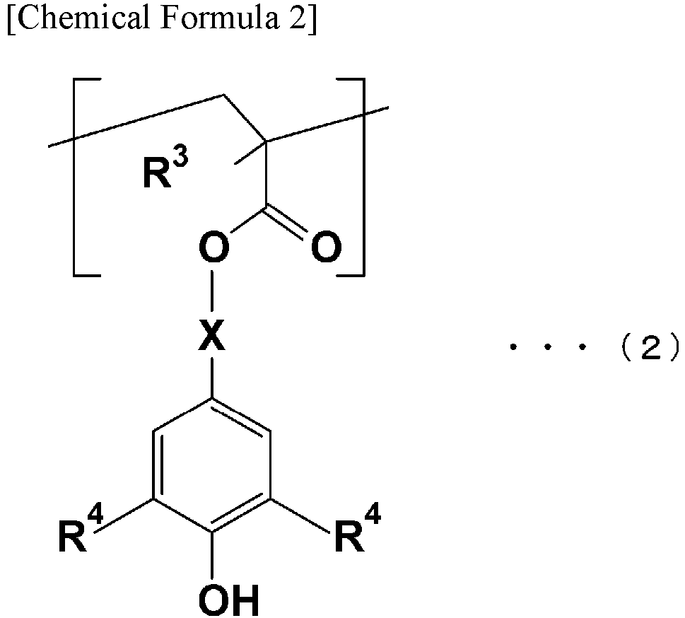
- According to a composition for forming a colored layer according to a fourth aspect of the present invention, in any one of the first to third aspects, the composition for forming the colored layer may further include one or more additives (E) selected from a radical scavenger, a peroxide decomposer, and a singlet oxygen quencher.
- According to a composition for forming a colored layer according to a fifth aspect of the present invention, in the fourth aspect, the singlet oxygen quencher may be a dialkyl phosphate, dialkyldithiocarbanate, or benzenedithiol, or a transition metal complex thereof.
- According to a composition for forming a colored layer according to a sixth aspect of the present invention, in any one of the first to fifth aspects, the dye (A) may contain one or more selected from the group consisting of compounds having a porphyrin structure, merocyanine structure, phthalocyanine structure, azo structure, cyanine structure, squarylium structure, coumarin structure, polyene structure, quinone structure, tetradiporphyrin structure, pyrromethene structure, and indigo structure; and a metal complex thereof.
- According to a composition for forming a colored layer according to a seventh aspect of the present invention, in any one of the first to sixth aspects, the dye (A) may further contain a third colorant whose wavelength of lowest transmittance within a wavelength range of 380 nm to 780 nm is within a range of 650 nm to 780 nm.
- An optical film according to an eighth aspect of the present invention includes a colored layer that is a cured product of the composition for forming the colored layer according to any one of the first to seventh aspects; a transparent substrate located on one surface of the colored layer; and a functional layer located on one or the other surface of the colored layer, wherein one or both of the transparent substrate and the functional layer have an ultraviolet shielding rate of 85% or higher as measured according to a method described in JIS L 1925, and the functional layer functions as an antireflection layer or an antiglare layer.
- According to an optical film according to a ninth aspect of the present invention, the optical film of the eighth aspect may further include an oxygen barrier layer having an oxygen permeability of 10 cm3/(m2·day·atm) or lower as the functional layer.
- According to an optical film according to a tenth aspect of the present invention, the optical film of the eighth or ninth aspect may further include an antistatic layer or an antifouling layer as the functional layer.
- A display device according to an eleventh aspect of the present invention includes the optical film according to any one of the eighth to tenth aspects.
- A composition for forming a colored layer according to a twelfth aspect of the present invention, the first aspect of the present invention contains a dye (A), an ionizing radiation-curable resin (B), a photoinitiator (C), and a solvent (D).
- The dye (A) contains at least one of a first colorant having a wavelength of maximum absorption in a first range of 470 nm to 530 nm, and an absorption spectrum with a full width at half maximum of 15 nm to 45 nm, a second colorant having a wavelength of maximum absorption in a second range of 560 to 620 nm, and an absorption spectrum with a full width at half maximum of 15 nm to 55 nm, and a third colorant whose wavelength of minimum transmittance within a wavelength range of 380 nm to 780 nm is within a third range of 650 nm or higher and 780 nm or lower.
- The minimum transmittance of this colorant composition is 1% or higher and lower than 50% in only one of the first to third ranges, and the ionizing radiation-curable resin (B) contains a resin having an amine structure.
- The ionizing radiation-curable resin (B) contains a resin having an amine structure.
- According to a composition for forming a colored layer according to a thirteenth aspect of the present invention, in the twelfth aspect, the ionizing radiation-curable resin (B) may be a polymer containing a structural unit represented by following formula (1),

- According to a composition for forming a colored layer according to a fourteenth aspect of the present invention, in the twelfth aspect, the ionizing radiation-curable resin (B) may further contain a polymer having a structural unit represented by following formula (2),

- A composition for forming a colored layer according to a fifteenth aspect of the present invention may further include, in any one of the twelfth to fourteenth aspects, an additive (E) including one or more selected from a radical scavenger, a peroxide decomposer, and a singlet oxygen quencher.
- According to a composition for forming a colored layer according to a sixteenth aspect of the present invention, in the fifteenth aspect, the singlet oxygen quencher may be a dialkyl phosphate, dialkyldithiocarbanate, or benzenedithiol, or a transition metal complex thereof.
- According to a composition for forming a colored layer according to a seventeenth aspect of the present invention, in any one of the twelfth to sixteenth aspects, the dye (A) may contain one or more selected from the group consisting of compounds having a porphyrin structure, merocyanine structure, phthalocyanine structure, azo structure, cyanine structure, squarylium structure, coumarin structure, polyene structure, quinone structure, tetradiporphyrin structure, pyrromethene structure, and indigo structure; and a metal complex thereof.
- An optical film according to an eighteenth aspect of the present invention includes a colored layer that is a cured product of the composition for forming the colored layer according to any one of the twelfth to seventeenth aspects; a transparent substrate located on one surface of the colored layer; and a functional layer located on one or the other surface of the colored layer.
- One or both of the transparent substrate and the functional layer have an ultraviolet shielding rate of 85% or higher as measured according to a method described in JIS L 1925.
- The functional layer functions as an antireflection layer or an antiglare layer.
- An optical film according to a nineteenth aspect of the present invention may further include, in the eighteenth aspect, an oxygen barrier layer having an oxygen permeability of 10 cm3/(m2·day·atm) or lower as the functional layer.
- An optical film according to a twentieth aspect of the present invention may further include, in the eighteenth or nineteenth aspect, an antistatic layer or an antifouling layer as the functional layer.
- A display device according to a twenty-first aspect of the present invention includes the optical film according to any one of the eighteenth to twentieth aspects.
- According to the first to eleventh aspects of the present invention, a composition for forming a colored layer, an optical film, and a display device capable of improving lightfastness and heat resistance, achieving both reflection suppression and luminance efficiency, improving display quality, extending the life of the light-emitting elements, and improving color reproducibility can be provided.
- According to the twelfth to twenty-first aspects of the present invention, a composition for forming a colored layer, an optical film, and a display device having a good color correction function and capable of withstanding long-term use can be provided.
-
-
Fig. 1 is a cross-sectional view of an optical film according to a first embodiment of the invention. -
Fig. 2 is a cross-sectional view of an optical film according to another embodiment of the invention. -
Fig. 3 is a cross-sectional view of an optical film according to another embodiment of the invention. -
Fig. 4 is a cross-sectional view of an optical film according to another embodiment of the invention. -
Fig. 5 is a cross-sectional view of an optical film according to another embodiment of the invention. -
Fig. 6 is a cross-sectional view of an optical film according to another embodiment of the invention. -
Fig. 7 is a cross-sectional view of an optical film according to another embodiment of the invention. -
Fig. 8 is a cross-sectional view of an optical film according to another embodiment of the invention. -
Fig. 9 is a graph showing the spectrum of a white display output from an organic EL light source and through a color filter used in the examples of the present invention. -
Fig. 10 is a graph showing the spectra during red, green, and blue displays output from the organic EL light source and through color filter used in the examples of the present invention. -
Fig. 11 is a graph showing a light transmission profile of a transparent substrate. -
Fig. 12 is a spectrum of a light source used to evaluate the transmission properties of the examples of the present invention. -
Fig. 13 is a spectrum of a light source used to evaluate the color reproducibility of the examples of the present invention. - With reference to the drawings, some embodiments of the present invention will be described. Throughout the drawings, the same reference signs are given to the same or corresponding components between different embodiments to omit duplicate description.
- Referring to
Fig. 1 , an optical film according to a first embodiment of the present invention will be described in detail. - As shown in
Fig. 1 , the optical film 1 includes acolored layer 10, atransparent substrate 20, and afunctional layer 30. Thefunctional layer 30 includes a lowrefractive index layer 31 and ahard coat layer 32. That is, the optical film 1 has thetransparent substrate 20 located on one surface of thecolored layer 10, and is a laminate in which thecolored layer 10, thetransparent substrate 20, thehard coat layer 32, and the lowrefractive index layer 31 are laminated in this order. - The thickness of the optical film 1 may be, for example, preferably in a range of 10 µm to 140 µm, more preferably 15 µm to 120 µm, and still more preferably 20 µm to 100 µm. When the thickness of the optical film 1 is equal to or greater than the lower limit, the strength of the optical film 1 can be further increased. When the thickness of the optical film 1 is equal to or less than the upper limit, not only the optical film 1 can be more lightweight but also the display device can be thinner.
- The following description addresses the individual layers forming the optical film 1.
- The
colored layer 10 is obtained by curing the composition for forming a colored layer of the present invention. The composition for forming a colored layer of the present invention contains a dye (A), an ionizing radiation-curable resin (B), a photoinitiator (C), and a solvent (D). The composition for forming a colored layer of the present invention may further contain an additive (E). - The thickness of the
colored layer 10 may be, for example, preferably 0.5 µm to 10 µm. When the thickness of thecolored layer 10 is equal to or greater than the lower limit, thecolored layer 10 can contain a dye to a degree not causing any abnormality in appearance, and the light absorption by the dye improves reflection characteristics and color reproducibility. When the thickness of thecolored layer 10 is equal to or less than the upper limit, it is advantageous in making the display device thinner. - The thickness of the
colored layer 10 is determined by observing the cross section of the optical film 1 in the thickness direction using a microscope or the like. - The dye (A) in the composition for forming a colored layer according to the above first to eleventh aspects of the present invention contains at least a first colorant and a second colorant.
- The wavelength of maximum absorption of the first colorant is within the range of 470 nm to 530 nm, and the full width at half maximum of the absorption spectrum is 15 nm to 45 nm. When the wavelength of maximum absorption is lower than the lower limit, the luminance efficiency for blue light emission is likely to decrease, and when it exceeds the upper limit, the luminance efficiency for green light emission is likely to decrease. When the full width at half maximum of the absorption spectrum is lower than the lower limit, the effect of suppressing external light reflection is reduced. On the other hand, when it exceeds the upper limit, the external light reflection characteristics tend to improve but the luminance efficiency is likely to decrease.
- The wavelength of maximum absorption of the second colorant is within the range of 560 nm to 620 nm, and the full width at half maximum of the absorption spectrum is 15 nm to 55 nm. When the wavelength of maximum absorption is lower than the lower limit, the luminance efficiency for green light emission is likely to decrease, and when it exceeds the upper limit, the luminance efficiency for red light emission is likely to decrease. When the full width at half maximum of the absorption spectrum is lower than the lower limit, the effect of suppressing external light reflection is reduced. On the other hand, when it exceeds the upper limit, the external light reflection characteristics tend to improve but the luminance efficiency is likely to decrease.
- The dye (A) may further contain another colorant other than the first and second colorants. The other colorant may be a third colorant.
- Within the wavelength range of 380 nm to 780 nm, the third colorant exhibits the lowest transmittance in the range of 650 nm to 780 nm. When the wavelength at which the transmittance of the third colorant is lowest within the wavelength range of 380 nm to 780 nm is lower than the lower limit, the luminance efficiency for red light emission is likely to decrease, and when it exceeds the upper limit, the effect of suppressing external light reflection decreases.
- The dye (A) in the composition for forming a colored layer according to the first to eleventh aspects of the present invention includes at least one of the following three types of colorants for selectively absorbing light in the wavelength range of visible light. It may include more than one type of colorant.
- The first colorant has a wavelength of maximum absorption within a first range of 470 nm to 530 nm, and the full width at half maximum of the absorption spectrum is 15 nm to 45 nm. When the wavelength of maximum absorption is lower than the lower limit, the luminance efficiency for blue light emission is likely to decrease, and when it exceeds the upper limit, the luminance efficiency for green light emission is likely to decrease. When the full width at half maximum of the absorption spectrum is lower than the lower limit, the effect of suppressing external light reflection is reduced. On the other hand, when it exceeds the upper limit, the external light reflection characteristics tend to improve but the luminance efficiency is likely to decrease.
- The second colorant has a wavelength of maximum absorption within a second range of 560 nm to 620 nm, and the full width at half maximum of the absorption spectrum is 15 nm to 55 nm. When the wavelength of maximum absorption is lower than the lower limit, the luminance efficiency for green light emission is likely to decrease, and when it exceeds the upper limit, the luminance efficiency for red light emission is likely to decrease. When the full width at half maximum of the absorption spectrum is lower than the lower limit, the effect of suppressing external light reflection is reduced. On the other hand, when it exceeds the upper limit, the external light reflection characteristics tend to improve but the luminance efficiency is likely to decrease.
- Within the wavelength range of 380 nm to 780 nm, the third colorant exhibits the lowest transmittance in a third range of 650 nm to 780 nm.
- The
colored layer 10 has a wavelength of maximum absorption at which the transmittance is 1% or higher and lower than 50% in only one of the first to third ranges. - By using colorants having the above-described absorption characteristics as the first to third colorants contained in the
colored layer 10, it is possible to form acolored layer 10 that absorbs a portion of the visible light emitted by the display device that is in a wavelength range in which the light emission intensity is relatively low. - The dye (A) preferably contains a compound having a porphyrin structure, merocyanine structure, phthalocyanine structure, azo structure, cyanine structure, squarylium structure, coumarin structure, polyene structure, quinone structure, tetradiporphyrin structure, pyrromethene structure, or indigo structure; or a metal complex thereof. In particular, it is more preferable to use a metal complex having a porphyrin structure, pyrromethene structure, or phthalocyanine structure, or a compound having a squarylium structure because of their high reliability. The dye (A) may contain only one of these compounds or metal complexes thereof, or two or more of them. These compounds or metal complexes thereof may be contained in the first, second, or third colorant, or in two or more of these colorants.
- The ionizing radiation-curable resin (B) is a resin that is cured by irradiating the resin with ionizing radiation such as ultraviolet light or electron beams for polymerization. For example, monofunctional, bifunctional, or trifunctional (meth)acrylate monomers or urethane (meth)acrylates, or those with more functional groups can be used, but the ionizing radiation-curable resin (B) of the present invention includes a resin that at least has the ability to scavenge radicals (radical scavenging ability). Here, "(meth)acrylate" means both or one of "acrylate" and "methacrylate".
- An example of a resin having radical scavenging ability included in the ionizing radiation-curable resin (B) is a resin having an amine structure. The "amine structure" refers to a structure in which the hydrogen atom of ammonia is replaced with a hydrocarbon group or an aromatic group. Examples of the amine structure include primary amine, secondary amine, and tertiary amine. It may also be a quaternary ammonium cation.
- The radical scavenging resin suppresses dye deterioration (fading) by scavenging radicals and suppressing autooxidation when the dye (A) undergoes oxidative deterioration. An example of a resin having a radical scavenging amine structure is a resin having a hindered amine structure and a molecular weight of 2,000 or more. When the molecular weight of the resin having a hindered amine structure is 2,000 or more, the effect of suppressing fading can be improved. This is considered to be because many molecules remain in the
colored layer 10, and thus a sufficient effect of suppressing fading can be obtained. - The upper limit of the molecular weight of the resin having a hindered amine structure is not particularly limited, and may be, for example, 50,000.
- The term "molecular weight" as used herein means "mass average molecular weight" measured by gel permeation chromatography (GPC) using polystyrene as the standard substance.
- The resin having a radical scavenging amine structure is preferably a polymer with a structural unit represented by the following formula (1).


- In formula (1), R1 represents a hydrogen atom, halogen atom, carboxyl group, sulfo group, cyano group, hydroxy group, alkyl group having 10 or fewer carbon atoms, alkoxycarbonyl group having 10 or fewer carbon atoms, alkylsulfonylaminocarbonyl group having 10 or fewer carbon atoms, arylsulfonylaminocarbonyl group, alkylsulfonyl group, arylsulfonyl group, acylaminosulfonyl group having 10 or fewer carbon atoms, alkoxy group having 10 or fewer carbon atoms, alkylthio group having 10 or fewer carbon atoms, aryloxy group having 10 or fewer carbon atoms, nitro group, alkoxycarbonyloxy group, aryloxycarbonyloxy group, acyloxy group having 10 or fewer carbon atoms, acyl group having 10 or fewer carbon atoms, carbamoyl group, sulfamoyl group, aryl group having 10 or fewer carbon atoms, substituted amino group, substituted ureido group, substituted phosphono group, or a heterocyclic group; R2 represents a hydrogen atom or an alkyl group having 30 or fewer carbon atoms; and X represents a single bond, an ester group, an aliphatic alkyl chain having 30 or fewer carbon atoms, an aromatic chain, a polyethylene glycol chain, or a linking group formed by combining them. Any of them may contain a spirodioxane ring.
- R1 is preferably a hydrogen atom, a hydroxy group, or an alkyl group having 10 or fewer carbon atoms. The number of carbon atoms in the alkyl group is preferably 1 to 6, more preferably 1 to 3.
- R2 is preferably a hydrogen atom or an alkyl group having 10 or fewer carbon atoms. The number of carbon atoms in the alkyl group is preferably 1 to 6, more preferably 1 to 3.
- X is preferably a single bond or an aliphatic alkyl chain having 30 or fewer carbon atoms. The number of carbon atoms in the aliphatic alkyl chain is preferably 10 or fewer, preferably 1 to 6, more preferably 2 to 4.
- In addition, the main component (the component with the highest mass%) of the resin having a radical scavenging amine structure is a copolymer of the structural unit represented by formula (1) and a copolymer component having one of the following repeating units. It becomes possible to control the compatibility with other components by being a copolymer.
- Examples of the repeating units include (meth)acrylate repeating units, olefin repeating units, halogen atom-containing repeating units, styrene repeating units, vinyl acetate repeating units, and vinyl alcohol repeating units.
- Examples of (meth)acrylate repeating units include repeating units derived from (meth)acrylate monomers having a linear or branched alkyl group in their side chains, and repeating units derived from (meth)acrylate monomers having a hydroxyl group in their side chains.
- Examples of the repeating units derived from (meth)acrylate monomers having a linear or branched alkyl group in their side chains include components derived from monomers such as methyl (meth)acrylate, ethyl (meth)acrylate, propyl (meth)acrylate, isopropyl (meth)acrylate, butyl (meth)acrylate, isobutyl (meth)acrylate, s-butyl (meth)acrylate, t-butyl (meth)acrylate, pentyl (meth)acrylate, hexyl (meth)acrylate, heptyl (meth)acrylate, octyl (meth)acrylate, isooctyl (meth)acrylate, 2-ethylhexyl acrylate, nonyl (meth)acrylate, isononyl (meth)acrylate, decyl (meth)acrylate, isodecyl (meth)acrylate, undecyl (meth)acrylate, dodecyl (meth)acrylate, tridecyl (meth)acrylate, tetradecyl (meth)acrylate, myristyl (meth)acrylate, pentadecyl (meth)acrylate, hexadecyl (meth)acrylate, heptadecyl (meth)acrylate, and octadecyl (meth)acrylate. These may be used alone or in combination of two or more. Among the above examples, (meth)acrylate repeating units having a linear or branched alkyl group with 1 to 4 carbon atoms in their side chains are preferable.
- Examples of the repeating units derived from (meth)acrylic monomers having a hydroxyl group in their side chains include components derived from monomers such as 2-hydroxyethyl (meth)acrylate, 2-hydroxypropyl (meth)acrylate, 4-hydroxybutyl (meth)acrylate, 6-hydroxyhexyl (meth)acrylate, and hydroxyphenyl (meth)acrylate. These may be used alone or in combination of two or more.
- Examples of olefinic repeating units include components derived from olefinic monomers such as ethylene, propylene, isoprene, and butadiene. These may be used alone or in combination of two or more.
- Examples of halogen atom-containing repeating units include components derived from monomers such as vinyl chloride and vinylidene chloride. These may be used alone or in combination of two or more.
- Examples of styrene repeating units include components derived from styrene monomers such as styrene, α-methylstyrene, and vinyltoluene. These may be used alone or in combination of two or more.
- Examples of vinyl acetate repeating units include esters of saturated carboxylic acids and vinyl alcohol such as vinyl acetate and vinyl propionate. These may be used alone or in combination of two or more.
- An example of a vinyl alcohol repeating unit is vinyl alcohol, and it may have a 1,2-glycol bond in its side chain.
- The copolymer may have the structure of a random copolymer, alternating copolymer, block copolymer or graft copolymer. The manufacturing process and preparation with other components are easy when the copolymer has the structure of a random copolymer. Therefore, a random copolymer is preferred to the other copolymers.
- Radical polymerization may be used as the polymerization method for obtaining the copolymer. Radical polymerization is preferable because it facilitates industrial production. The radical polymerization may be solution polymerization, emulsion polymerization, bulk polymerization, or suspension polymerization. The radical polymerization is preferably solution polymerization. By using solution polymerization, the molecular weight of the copolymer can be easily controlled.
- In radical polymerization, before adding a polymerization initiator to polymerize the monomers, the monomers may be diluted with a polymerization solvent.
- The polymerization solvent may be, for example, an ester solvent, alcohol ether solvent, ketone solvent, aromatic solvent, amide solvent, or alcohol solvent. The ester solvent may be, for example, methyl acetate, ethyl acetate, n-butyl acetate, isobutyl acetate, t-butyl acetate, methyl lactate, or ethyl lactate. The alcohol ether solvent may be, for example, ethylene glycol monomethyl ether, ethylene glycol monoethyl ether, propylene glycol monomethyl ether, propylene glycol monomethyl ether acetate, propylene glycol monoethyl ether, 3-methoxy-1-butanol, or 3-methoxy-3-methyl-1-butanol. The ketone solvent may be, for example, acetone, methyl ethyl ketone, methyl isobutyl ketone, or cyclohexanone. The aromatic solvent may be, for example, benzene, toluene, or xylene. The amide solvent may be, for example, formamide or dimethylformamide. The alcohol solvent may be, for example, methanol, ethanol, n-propanol, isopropanol, n-butanol, isobutanol, s-butanol, t-butanol, diacetone alcohol, or 2-methyl-2-butanol. One of the polymerization solvents described above may be used alone or two or more may be mixed together.
- The radical polymerization initiator may be, for example, a peroxide or an azo compound. The peroxide may be, for example, benzoyl peroxide, t-butyl peroxyacetate, t-butyl peroxybenzoate, or di-t-butyl peroxide. The azo compound may be, for example, azobisisobutyronitrile, an azobisamidinopropane salt, an azobiscyanovaleric acid (salt), or 2,2'-azobis[2-methyl-N-(2-hydroxyethyl) propionamide].
- When the resin having a radical scavenging amine structure is a polymer with the structural unit represented by formula (1), the content of the structural unit represented by formula (1) is preferably 1 to 100 mol%, more preferably 35 to 100 mol% relative to the total molar quantity of the monomers constituting the ionizing radiation-curable resin (B). When the content of the structural unit represented by formula (1) is within this range, the lightfastness and heat resistance of the dye (A) are improved, which in turn assists suppressing fading.
- The ionizing radiation-curable resin (B) may further contain a polymer having a structural unit represented by the following formula (2).


- In formula (2), R3 represents a hydrogen atom, halogen atom, carboxyl group, sulfo group, cyano group, hydroxy group, alkyl group having 10 or fewer carbon atoms, alkoxycarbonyl group having 10 or fewer carbon atoms, alkylsulfonylaminocarbonyl group having 10 or fewer carbon atoms, arylsulfonylaminocarbonyl group, alkylsulfonyl group, arylsulfonyl group, acylaminosulfonyl group having 10 or fewer carbon atoms, alkoxy group having 10 or fewer carbon atoms, alkylthio group having 10 or fewer carbon atoms, aryloxy group having 10 or fewer carbon atoms, nitro group, alkoxycarbonyloxy group, aryloxycarbonyloxy group, acyloxy group having 10 or fewer carbon atoms, acyl group having 10 or fewer carbon atoms, carbamoyl group, sulfamoyl group, aryl group having 10 or fewer carbon atoms, substituted amino group, substituted ureido group, substituted phosphono group, or a heterocyclic group; R4 represents a hydrogen atom or an alkyl group having 30 or fewer carbon atoms; and X represents a single bond, an ester group, an aliphatic alkyl chain having 30 or fewer carbon atoms, an aromatic chain, a polyethylene glycol chain, or a linking group formed by combining them. Any of them may contain a spirodioxane ring.
- R3 is preferably a hydrogen atom, a hydroxy group, or an alkyl group having 10 or fewer carbon atoms. The number of carbon atoms in the alkyl group is preferably 1 to 6, more preferably 1 to 3.
- R4 is preferably a hydrogen atom or an alkyl group having 10 or fewer carbon atoms. The number of carbon atoms in the alkyl group is preferably 1 to 6, more preferably 1 to 3.
- X is preferably a single bond or an aliphatic alkyl chain having 30 or fewer carbon atoms. The number of carbon atoms in the aliphatic alkyl chain is preferably 10 or fewer, preferably 1 to 6, more preferably 2 to 4.
- In this embodiment, the polymer having the structural unit represented by formula (2) may be a copolymer with a monomer that is different from the structural unit represented by formula (2). It becomes possible to control the compatibility with other components by being a copolymer.
- The copolymer component may be, for example, a component including one of the above-described (meth)acrylate repeating units, olefin repeating units, halogen atom-containing repeating units, styrene repeating units, vinyl acetate repeating units, and vinyl alcohol repeating units.
- The copolymer may have the structure of a random copolymer, alternating copolymer, block copolymer or graft copolymer. The manufacturing process and preparation with other components are easy when the copolymer has the structure of a random copolymer. Therefore, a random copolymer is preferred to the other copolymers.
- Radical polymerization may be used as the polymerization method for obtaining the copolymer. Radical polymerization is preferable because it facilitates industrial production. The radical polymerization may be solution polymerization, emulsion polymerization, bulk polymerization, or suspension polymerization. The radical polymerization is preferably solution polymerization. By using solution polymerization, the molecular weight of the copolymer can be easily controlled.
- In radical polymerization, before adding a polymerization initiator to polymerize the monomers, the monomers may be diluted with a polymerization solvent.
- The polymerization solvent may be, for example, an ester solvent, alcohol ether solvent, ketone solvent, aromatic solvent, amide solvent, or alcohol solvent. The ester solvent may be, for example, methyl acetate, ethyl acetate, n-butyl acetate, isobutyl acetate, t-butyl acetate, methyl lactate, or ethyl lactate. The alcohol ether solvent may be, for example, ethylene glycol monomethyl ether, ethylene glycol monoethyl ether, propylene glycol monomethyl ether, propylene glycol monomethyl ether acetate, propylene glycol monoethyl ether, 3-methoxy-1-butanol, or 3-methoxy-3-methyl-1-butanol. The ketone solvent may be, for example, acetone, methyl ethyl ketone, methyl isobutyl ketone, or cyclohexanone. The aromatic solvent may be, for example, benzene, toluene, or xylene. The amide solvent may be, for example, formamide or dimethylformamide. The alcohol solvent may be, for example, methanol, ethanol, n-propanol, isopropanol, n-butanol, isobutanol, s-butanol, t-butanol, diacetone alcohol, or 2-methyl-2-butanol. One of the polymerization solvents described above may be used alone or two or more may be mixed together.
- The radical polymerization initiator may be, for example, a peroxide or an azo compound. The peroxide may be, for example, benzoyl peroxide, t-butyl peroxyacetate, t-butyl peroxybenzoate, or di-t-butyl peroxide. The azo compound may be, for example, azobisisobutyronitrile, an azobisamidinopropane salt, an azobiscyanovaleric acid (salt), or 2,2'-azobis[2-methyl-N-(2-hydroxyethyl) propionamide].
- When the total amount of monomers is taken as 100 parts by mass, the amount of the radical polymerization initiator is preferably 0.0001 parts by mass or more and 20 parts by mass or less, more preferably 0.001 parts by mass or more and 15 parts by mass or less, and further preferably 0.005 parts by mass or more and 10 parts by mass or less. The radical polymerization initiator may be added to the monomers and the polymerization solvent before initiating polymerization, or may be dropped into the polymerization reaction system. Dropping the radical polymerization initiator into the polymerization reaction system for the monomers and the polymerization solvent is preferable in that the heat generation caused by polymerization can be suppressed.
- The reaction temperature for radical polymerization is selected as appropriate according to the types of radical polymerization initiator and polymerization solvent. The reaction temperature is preferably 60°C or higher and 110°C or lower in order to facilitate manufacturing and reaction control.
- When the ionizing radiation-curable resin (B) contains a polymer having the structural unit represented by formula (2), the content of the structural unit represented by formula (2) is preferably 1 to 50 mol%, more preferably 1 to 30 mol% relative to the total molar quantity of the monomers constituting the ionizing radiation-curable resin (B). When the content of the structural unit represented by formula (2) is within this range, the lightfastness and heat resistance of the dye (A) are improved, which in turn assists suppressing fading.
- Examples of the monofunctional (meth)acrylate compound the ionizing radiation-curable resin (B) may contain include 2-hydroxyethyl (meth)acrylate, 2-hydroxypropyl (meth)acrylate, 2-hydroxybutyl (meth)acrylate, n-butyl (meth)acrylate, isobutyl (meth)acrylate, t-butyl (meth)acrylate, glycidyl (meth)acrylate, acryloylmorpholine, N-vinylpyrrolidone, tetrahydrofurfuryl acrylate, cyclohexyl (meth)acrylate, 2-ethylhexyl (meth)acrylate, isobornyl (meth)acrylate, isodecyl (meth)acrylate, lauryl (meth)acrylate, tridecyl (meth)acrylate, cetyl (meth)acrylate, stearyl (meth)acrylate, benzyl (meth)acrylate, 2-ethoxyethyl (meth)acrylate, 3-methoxybutyl (meth)acrylate, ethyl carbitol (meth)acrylate, phosphate (meth)acrylate, ethylene-oxide-modified phosphate (meth)acrylate, phenoxy (meth)acrylate, ethylene-oxide-modified phenoxy (meth)acrylate, propylene-oxide-modified phenoxy (meth)acrylate, nonyl phenol (meth)acrylate, ethylene-oxide-modified nonyl phenol (meth)acrylate, propylene-oxide-modified nonyl phenol (meth)acrylate, methoxy diethylene glycol (meth)acrylate, methoxy polyethylene glycol (meth)acrylate, methoxy propylene glycol (meth)acrylate, 2-(meth)acryloyl oxyethyl-2-hydroxy propyl phthalate, 2-hydroxy-3-phenoxy propyl (meth)acrylate, 2-(meth)acryloyl oxyethyl hydrogen phthalate, 2-(meth)acryloyl oxypropyl hydrogen phthalate, 2-(meth)acryloyl oxypropyl hexahydro hydrogen phthalate, 2-(meth)acrylol oxypropyl tetrahydro hydrogen phthalate, dimethylaminoethyl (meth)acrylate, trifluoroethyl (meth)acrylate, tetrafluoropropyl (meth)acrylate, hexafluoropropyl (meth)acrylate, octafluoropropyl (meth)acrylate, and adamantine derivative mono(meth)acrylate, such as adamanthyl acrylate having monovalent mono(meth)acrylate which is derived from 2-adamantane and adamantine diol. Here, "(meth)acryloyl" means both or one of "acryloyl" and "methacryloyl".
- Examples of the bifunctional (meth)acrylate compound the ionizing radiation-curable resin (B) may contain include di(meth)acrylates, such as ethylene glycol di(meth)acrylate, diethylene glycol di(meth)acrylate, butanediol di(meth)acrylate, hexanediol di(meth)acrylate, nonanediol di(meth)acrylate, ethoxylated hexanediol di(meth)acrylate, propoxylated hexanediol di(meth)acrylate, diethylene glycol di(meth)acrylate, polyethylene glycol di(meth)acrylate, tripropylene glycol di(meth)acrylate, polypropylene glycol di(meth)acrylate, neopentyl glycol di(meth)acrylate, ethoxylated neopentyl glycol di(meth)acrylate, tripropylene glycol di(meth)acrylate, and hydroxy pivalate neopentyl glycol di(meth)acrylate.
- Examples of the trifunctional (meth)acrylate compound or (meth)acrylate compound having more functional groups that the ionizing radiation-curable resin (B) may contain include tri(meth)acrylates such as trimethylolpropane tri(meth)acrylate, ethoxylated trimethylolpropane tri(meth)acrylate, propoxylated trimethylolpropane tri(meth)acrylate, tris2-hydroxyethylisocyanurate tri(meth)acrylate or glycerin tri(meth)acrylate, trifunctional (meth)acrylate compounds such as pentaerythritol tri(meth)acrylate, dipentaerythritol tri(meth)acrylate or ditrimethylolpropane tri(meth)acrylate, polyfunctional (meth)acrylate compounds having three or more functional groups such as pentaerythritol tetra(meth)acrylate, ditrimethylolpropane tetra(meth)acrylate, dipentaerythritol tetra(meth)acrylate, dipentaerythritol penta(meth)acrylate, ditrimethylolpropane penta(meth)acrylate, dipentaerythritol hexa(meth)acrylate or ditrimethylolpropane hexa(meth)acrylate, and polyfunctional (meth)acrylate compounds obtained by substituting part of these (meth)acrylate substituted with an alkyl group or ε-caprolactone.
- Urethane (meth)acrylate can also be used as the resin that the ionizing radiation-curable resin (B) may contain. Examples of urethane (meth)acrylate include those obtained by reacting a (meth)acrylate monomer having a hydroxyl group with a product of the reaction between a polyester polyol with an isocyanate monomer or a prepolymer.
- Examples of urethane (meth)acrylate include a pentaerythritol triacrylate hexamethylene diisocyanate urethane prepolymer, dipentaerythritol pentaacrylate hexamethylene diisocyanate urethane prepolymer, pentaerythritol triacrylate toluene diisocyanate urethane prepolymer, dipentaerythritol pentaacrylate toluene diisocyanate urethane prepolymer, pentaerythritol triacrylate isophorone diisocyanate urethane prepolymer, and dipentaerythritol pentaacrylate isophorone diisocyanate urethane prepolymer.
- The above-listed other monofunctional, bifunctional, or trifunctional (meth)acrylate monomers or urethane (meth)acrylates, those with more functional groups, or the like that the ionizing radiation-curable resin (B) can contain may be used alone or in combination of two or more. It may also be a partially polymerized oligomer.
- The content of the ionizing radiation-curable resin (B) is preferably 20 to 80% by mass, more preferably 30 to 70% by mass relative to the total mass of the composition for forming the colored layer. When the content of the ionizing radiation-curable resin (B) is equal to or more than the lower limit, the effect of suppressing fading can be further enhanced. When the content of the ionizing radiation-curable resin (B) is equal to or lower than the upper limit, the composition for forming the colored layer can be handled even easier.
- For example, when ultraviolet light is used as the ionizing radiation, the photoinitiator (C) generates radicals when ultraviolet light is irradiated.
- Examples of photoinitiators (C) include benzoins (including benzoin and benzoin alkyl ethers such as benzoin methyl ether, benzoin ethyl ether, and benzoin isopropyl ether), phenyl ketones [for example, acetophenones (including acetophenone, 2-hydroxy-2-methyl-1-phenylpropane-1-one, 2,2-dimethoxy-2-phenylacetophenone, 2,2-diethoxy-2-phenylacetophenone, and 1,1-dichloroacetophenone), alkylphenyl ketones such as 2-hydroxy-2-methylpropiophenone; and cycloalkylphenyl ketones such as 1-hydroxycyclohexylphenyl ketone], aminoacetophenones {including 2-methyl-1-[4-(methylthio)phenyl]-2-morpholinoaminopropanone-1,2-benzyl -2-dimethylamino-1-(4-morpholinophenyl)-butanone-1}, anthraquinones (including anthraquinone, 2-methylanthraquinone, 2-ethylanthraquinone, 2-t-butylanthraquinone, and 1-chloroanthraquinone), thioxanthones (including 2,4-dimethylthioxanthone, 2,4-diethylthioxanthone, 2-chlorothioxanthone, and 2,4-diisopropylthioxanthone), ketals (including acetophenone dimethyl ketal and benzyl dimethyl ketal), benzophenones (including benzophenone), xanthones, and phosphine oxides (for example, 2,4,6-trimethylbenzoyldiphenylphosphine oxide). These photoinitiators may be used singly or in combination of two or more.
- The content of the photoinitiator (C) is preferably 0.01 to 20 mass%, more preferably 0.01 to 5 mass% relative to the solid content of the composition for forming the colored layer. When the content of the photoinitiator (C) is less than the lower limit, the curing effect will be insufficient. When the content of the photoinitiator (C) exceeds the upper limit, part of the photoinitiator (C) remains unreacted and degrades the reliability of properties such as heat resistance.
- Examples of the solvent (D) include ethers, ketones, esters, and cellosolves. Examples of ethers include dibutyl ether, dimethoxymethane, dimethoxyethane, diethoxyethane, propylene oxide, 1,4-dioxane, 1,3-dioxolane, 1,3,5-trioxane, tetrahydrofuran, anisole, and phenetole. Examples of ketones include acetone, methyl ethyl ketone, diethyl ketone, dipropyl ketone, diisobutyl ketone, methyl isobutyl ketone, cyclopentanone, cyclohexanone, methylcyclohexanone, and ethylcyclohexanone. Examples of esters include ethyl formate, propyl formate, n-pentyl formate, methyl acetate, ethyl acetate, methyl propionate, ethyl propionate, n-pentyl acetate, and γ-butyrolactone. Examples of cellosolves include methyl cellosolve, cellosolve (ethyl cellosolve), butyl cellosolve, and cellosolve acetate. One or a combination of two or more of the solvents (D) may be used.
- The content of the solvent (D) is preferably 20 to 80 mass%, more preferably 30 to 70 mass% relative to the total mass of the composition for forming the colored layer. When the content of the solvent (D) is equal to or more than the lower limit, the composition for forming the colored layer can be handled even easier. When the content of the solvent (D) is equal to or lower than the upper limit, the time required to form the colored layer can be reduced.
- The additive (E) may be one or more selected from a radical scavenger, a peroxide decomposer, and a singlet oxygen quencher.
- Examples of radical scavengers include hindered amine photostabilizers such as 4-isopropylaminodiphenylamine, N-phenyl-1-naphthylamine, and 1,2,2,6,6-pentamethyl-4-piperidyl methacrylate; and phenolic antioxidants such as 2,6-di-t-butyl-p-cresol and 6,6'-di-t-butyl-4,4'-butylidenedi-m-cresol.
- Examples of peroxide decomposers include sulfur-based antioxidants such as ditridecyl-3,3'-thiodipropionate, 2-mercaptobenzothiazole, and 2-mercaptobenzimidazole; and phosphite-based antioxidants such as tris(nonylphenyl)phosphite and 2-ethylhexyl diphenyl phosphite.
- Examples of singlet oxygen quenchers include dialkyl phosphates, dialkyldithiocarbanates, benzenedithiols, and transition metal complexes of similar dithiols.
- One or a combination of two or more of the additives (E) may be used.
- Other additives such as a leveling agent, antifoaming agent, antioxidant, ultraviolet absorber, photostabilizer, photosensitizer, and conductive material may be used as the additive (E).
- The content of the additive (E) is preferably 0.1 to 20 mass%, more preferably 0.1 to 15 mass% relative to the solid content of the composition for forming the colored layer. When the content of the additive (E) is less than the lower limit, the effect of suppressing fading is not obtained with regard to the lightfastness and heat resistance of the dye (A). When the content of the additive (E) exceeds the upper limit, it tends to lead to insufficient curing due to curing inhibition by the additive (E) and/or a decreased amount of the curing component.
- By containing the composition for forming a colored layer of the present invention, the
colored layer 10 improves lightfastness and heat resistance, and in the first to eleventh aspects described above, it is possible to achieve both reflection suppression and luminance efficiency, improve display quality, extend the life of the light emitting elements, and improve color reproducibility. - In the twelfth to twenty-first aspects, the color correction function can be maintained for a long time.
- The
transparent substrate 20 is a sheet-like member located on one surface of thecolored layer 10 and forming an optical film 1. - A resin film having translucency may be used as the
transparent substrate 20.
The forming material of thetransparent substrate 20 may be a transparent resin or inorganic glass. Examples of transparent resin include polyolefin, polyester, polyacrylate, polyamide, polyimide, polyarylate, polycarbonate, triacetyl cellulose, polyvinyl alcohol, polyvinyl chloride, cycloolefin copolymer, norbornene-containing resin, polyether sulfone, and polysulfone. Examples of polyolefins include polyethylene and polypropylene. Examples of polyesters include polyethylene terephthalate, polybutylene terephthalate, and polyethylene naphthalate. An example of polyacrylate is polymethyl methacrylate. Examples of polyamides include nylon 6 and nylon 66. Among these, suitable examples are a film of polyethylene terephthalate (PET), a film of triacetyl cellulose (TAC), a film of polymethyl methacrylate (PMMA), and a film of polyester other than PET. - Although the thickness of the
transparent substrate 20 is not specifically limited, it is preferably in a range of 10 µm to 100 µm, for example. - The transmittance of the
transparent substrate 20 is preferably, for example, 90% or higher. - The
transparent substrate 20 may be provided with the ability to absorb ultraviolet light. Thetransparent substrate 20 can be given the ability to absorb ultraviolet light by adding an ultraviolet absorber to the resin material of thetransparent substrate 20. - Examples of ultraviolet absorbers include salicylic acid ester ultraviolet absorbers, benzophenone ultraviolet absorbers, benzotriazole ultraviolet absorbers, benzotriazine ultraviolet absorbers, and cyanoacrylate ultraviolet absorbers.
- These ultraviolet absorbers may be used singly or in combination of two or more.
- When the
transparent substrate 20 is provided with the ability to absorb ultraviolet light, it preferably has an ultraviolet shielding rate of 85% or higher. The ultraviolet shielding rate is a value measured in accordance with JIS L 1925, and is calculated by the following formula (I).Ultraviolet shielding rate (%) = 100 - Average transmittance of ultraviolet light with a wavelength of 290 nm to 400 nm (%) - An ultraviolet shielding rate below 85% reduces the effect of suppressing fading with regard to the lightfastness of the dye (A).
-
Fig. 11 shows the light transmission profiles of polymethyl methacrylate (PMMA), triacetyl cellulose (TAC), and polyethylene terephthalate (PET) that have been given the ability to absorb ultraviolet light. The ultraviolet shielding rates of the transparent substrates shown by the light transmission profiles inFig. 11 are as follows. Any of them can be suitably used as thetransparent substrate 20 of the present invention. - The
functional layer 30 is located on one or the other surface of thecolored layer 10. By having thefunctional layer 30, the optical film can exhibit various functions. - Examples of the functions of the
functional layer 30 include antireflection function, antiglare function, oxygen barrier function, antistatic function, antifouling function, reinforcement function, and ultraviolet absorption function (ability to absorb ultraviolet light). - The
functional layer 30 may be a monolayer or a multilayer. Thefunctional layer 30 may have one function or two or more functions. - When the optical film 1 has an antireflection function, the
functional layer 30 functions as an antireflection layer. Examples of the antireflection layer include a lowrefractive index layer 31 having a lower refractive index than ahard coat layer 32, anantiglare layer 34, and thetransparent substrate 20, which will be described later. The lowrefractive index layer 31 can be formed by using, for the functional layer, a material having a lower refractive index than the materials of thehard coat layer 32, theantiglare layer 34, and thetransparent substrate 20. - To adjust the refractive index of the low
refractive index layer 31, fine particles of lithium fluoride (LiF), magnesium fluoride (MgF2), sodium hexafluoroaluminum (cryolite, 3NaF·AlF3, Na3AlF6), or aluminum fluoride (AlF3), or fine silica particles may be added. It is effective to use particles having internal voids, such as fine, porous silica particles or hollow silica particles, as the fine silica particles to reduce the refractive index of the lowrefractive index layer 31. The photoinitiator (C), solvent (D), or additive (E) described in relation to thecolored layer 10 may be added to the composition for forming the low refractive index layer 31 (composition for forming a low refractive index layer) as appropriate. - The refractive index of the low
refractive index layer 31 is preferably 1.20 to 1.55. - Although the thickness of the low
refractive index layer 31 is not specifically limited, it is preferably in a range of 40 nm to 1 µm, for example. - When the optical film 1 has an antiglare function, the
functional layer 30 functions as anantiglare layer 34. - The
antiglare layer 34 has small irregularities on its surface so that they scatter external light to suppress reflection and in turn improve display quality. When combined with the lowrefractive index layer 31, the lowrefractive index layer 31 and theantiglare layer 34 constitute an antireflection layer. - The
antiglare layer 34 contains at least one selected from fine organic particles and fine inorganic particles as necessary. The fine organic particles are materials that form small irregularities on the surface and provide the function of scattering external light. Examples of fine organic particles include resin particles of translucent resin materials such as acrylic resin, polystyrene resin, styrene-(meth)acrylate copolymers, polyethylene resin, epoxy resin, silicone resin, polyvinylidene fluoride, and polyethylene fluoride resin. In order to adjust the refractive index and the dispersibility of resin particles, two or more types of resin particles having different characteristics (refractive indexes) may be mixed. - The fine inorganic particles are a material for controlling sedimentation and aggregation of the fine organic particles. Examples of fine inorganic particles include fine silica particles, fine metal oxide particles, and fine particles of various minerals. Examples of fine silica particles include colloidal silica, and fine silica particles surface-modified with a reactive functional group such as an (meth)acryloyl group. Examples of fine metal oxide particles include fine particles of alumina (aluminum oxide), zinc oxide, tin oxide, antimony oxide, indium oxide, titania (titanium dioxide), and zirconia (zirconium dioxide). Examples of fine mineral particles include fine particles of mica, synthetic mica, vermiculite, montmorillonite, iron-montmorillonite, bentonite, beidellite, saponite, hectorite, stevensite, nontronite, magadiite, ilerite, kanemite, layered titanate, smectite, and synthetic smectite. The fine mineral particles may either be natural or synthetic (including substituted products and derivatives), and also a mixture of both may be used. Among these fine mineral particles, organic layered clay is more preferable.
- Organic layered clay refers to a swelling clay in which organic onium ions are introduced between layers. The organic onium ion is not particularly limited as long as it can make a swelling clay organic by using the cation exchange properties of the swelling clay. When an organic layered clay mineral is used as the fine mineral particles, the synthetic smectite can be suitably used. Synthetic smectite has a function of increasing the viscosity of the coating liquid for forming the antiglare layer. This suppresses the sedimentation of resin particles and fine inorganic particles and adjusts the shape of the irregularities on the surface of the antiglare layer 34 (functional layer 30).
- When the optical film 1 has an oxygen barrier function, the
functional layer 30 functions as anoxygen barrier layer 33. Theoxygen barrier layer 33 has an oxygen permeability of 10 cm3/(m2·day·atm) or lower, preferably 5 cm3/(m2·day·atm) or lower, and more preferably 1 cm3/(m2·day·atm) or lower. When the oxygen permeability of theoxygen barrier layer 33 is equal to or lower than the upper limit, thefunctional layer 30 can be provided with a sufficient oxygen barrier function. The lower limit of the oxygen permeability of theoxygen barrier layer 33 is not particularly limited, and may be 0 cm3/(m2·day·atm). - The oxygen permeability of the
oxygen barrier layer 33 is a value measured using an oxygen permeability measuring device at 30°C and a relative humidity of 60%. - When the optical film 1 has an antistatic function, the
functional layer 30 functions as an antistatic layer. Examples of the antistatic layer include layers containing antistatic agents such as fine metal oxide particles such as antimony-doped tin oxide (ATO) and tin-doped indium oxide (ITO), polymeric conductive compositions, and quaternary ammonium salts. - The antistatic layer may be provided on the outermost surface of the
functional layer 30 or between thefunctional layer 30 and thetransparent substrate 20. Alternatively, the antistatic layer may be formed by adding an antistatic agent to one of the above-described layers constituting thefunctional layer 30. When an antistatic layer is provided, the optical film preferably has a surface resistance of 1.0×10⁶ to 1.0×10¹² (Ω/cm). - When the optical film 1 has an antifouling function, the
functional layer 30 functions as an antifouling layer. The antifouling layer improves the antifouling performance by imparting both or one of water repellency and oil repellency. Examples of the antifouling layer include layers containing antifouling agents such as silicon oxide, fluorine-containing silane compounds, fluoroalkylsilazane, fluoroalkylsilane, fluorine-containing silicon compounds, and perfluoropolyether group-containing silane coupling agents. - The antifouling layer may be provided on the outermost surface of the
functional layer 30, or formed by adding an antifouling agent to the outermost layer of the functional layer(s) 30. - When the optical film 1 has a reinforcement function, the
functional layer 30 functions as a reinforcement layer. The reinforcement layer is a layer that reinforces the optical film. An example of the reinforcement layer is thehard coat layer 32. Examples of thehard coat layer 32 include layers formed with a hard coat agent containing monofunctional, bifunctional, or trifunctional (meth)acrylate or urethane (meth)acrylate, or (meth)acrylate or urethane (meth)acrylate with more functional groups. - When the optical film 1 has the ability to absorb ultraviolet light, the
functional layer 30 functions as an ultraviolet absorbing layer. Examples of the ultraviolet absorbing layer include layers containing triazine ultraviolet absorbers such as 2-(4,6-diphenyl-1,3,5-triazin-2-yl)-5-hexyloxyphenol and benzotriazole ultraviolet absorbers such as 2-(2H-benzotriazole-2-yl)-4-methylphenol. - The content of the ultraviolet absorber is preferably 0.1 to 5 mass% relative to the total mass of the materials forming the ultraviolet absorbing layer. When the content of the ultraviolet absorber is equal to or more than the lower limit, the
functional layer 30 can be provided with sufficient ultraviolet absorbance. When the content of the ultraviolet absorber is equal to or lower than the upper limit, it is possible to avoid insufficient hardness due to a decrease in the amount of the curing component. - In the optical film 1, one or both of the
transparent substrate 20 and thefunctional layer 30 have an ultraviolet shielding rate of 85% or higher, preferably 90% or higher, more preferably 95% or higher. It may even be 100%. When the ultraviolet shielding rate is equal to or higher than the lower limit, lightfastness and heat resistance can be further improved. - The ultraviolet shielding rate can be measured according to the method described in JIS L 1925.
- The ultraviolet shielding rate can be adjusted by imparting ultraviolet absorbing ability to one or both of the
transparent substrate 20 and thefunctional layer 30. - The thickness of the
functional layer 30 may be, for example, preferably in a range of 0.04 µm to 25 µm, more preferably 0.1 µm to 20 µm, and still more preferably 0.2 µm to 15 µm. When the thickness of thefunctional layer 30 is equal to or greater than the lower limit, it becomes easier to impart various functions to the optical film 1. When the thickness of thefunctional layer 30 is equal to or less than the upper limit, it is advantageous in making the display device thinner. - The optical film 1 of this embodiment can be manufactured by a conventionally known method.
- For example, the
colored layer 10 is obtained by applying a composition for forming the colored layer to one surface of thetransparent substrate 20 and curing the composition by irradiating it with ionizing radiation. - The light source for irradiating the composition for forming the colored layer with ionizing radiation to cure it and form the
colored layer 10 can be any light source that generates ionizing radiation. Examples of the ionizing radiation include optical energy radiation such as radiation (such as gamma rays and X-rays), ultraviolet light, visible light, and electron beams (EB). Usually ultraviolet light and electron beams are used. Examples of lamps emitting ultraviolet light include low-pressure mercury vapor lamps, medium-pressure mercury vapor lamps, high-pressure mercury vapor lamps, carbon arc lamps, metal halide lamps, xenon lamps, and electrodeless lamps. The ultraviolet light is usually irradiated at 100 to 1000 mJ/cm2. - Next, a hard coat agent is applied to the other surface of the
transparent substrate 20. As with thecolored layer 10, the applied hard coat agent is irradiated with ionizing radiation to cure it, thereby obtaining thehard coat layer 32. - By forming the low
refractive index layer 31 on thehard coat layer 32, an optical film 1 having thefunctional layer 30 on the other surface of thetransparent substrate 20 can be obtained. - The method of forming the low
refractive index layer 31 is not particularly limited. For example, it may be formed by applying a composition for forming a low refractive index layer to thehard coat layer 32 and irradiating the applied composition with ionizing radiation to cure it, vacuum evaporation, sputtering, ion plating, an ion beam method, or plasma-enhanced chemical vapor deposition. - As shown in
Fig. 2 , the optical film may be an optical film 2 in which thetransparent substrate 20 is located on one surface of thecolored layer 10, and thecolored layer 10, thetransparent substrate 20, theoxygen barrier layer 33, thehard coat layer 32, and the lowrefractive index layer 31 are laminated in this order. In the optical film 2, theoxygen barrier layer 33, thehard coat layer 32, and the lowrefractive index layer 31 constitute thefunctional layer 30. - Since the optical film 2 of this embodiment has the
oxygen barrier layer 33, it exhibits better oxygen barrier performance than the optical film 1. - As shown in
Fig. 3 , the optical film may be anoptical film 3 in which thetransparent substrate 20 is located on one surface of thecolored layer 10, and thecolored layer 10, thetransparent substrate 20, and theantiglare layer 34 are laminated in this order. In theoptical film 3, theantiglare layer 34 forms thefunctional layer 30. - Since the
optical film 3 of this embodiment has theantiglare layer 34, it suppresses reflection well. - As shown in
Fig. 4 , the optical film may be an optical film 4 in which thetransparent substrate 20 is located on one surface of thecolored layer 10, and thecolored layer 10, thetransparent substrate 20, theantiglare layer 34, and the lowrefractive index layer 31 are laminated in this order. In the optical film 4, theantiglare layer 34 and the lowrefractive index layer 31 constitute thefunctional layer 30. - Since the optical film 4 of this embodiment has the low
refractive index layer 31 and theantiglare layer 34, it suppresses reflection even better. - As shown in
Fig. 5 , the optical film may be anoptical film 5 in which thetransparent substrate 20 is located on one surface of thecolored layer 10, and thefunctional layer 30 is located on the other surface of thecolored layer 10. In theoptical film 5, thetransparent substrate 20, thecolored layer 10, thehard coat layer 32, and the lowrefractive index layer 31 are laminated in this order. In theoptical film 5, thehard coat layer 32 and the lowrefractive index layer 31 constitute thefunctional layer 30. - The
optical film 5 of this embodiment has the coloredlayer 10 and thefunctional layer 30 having an ultraviolet absorbing function and an antireflection function on one surface of thetransparent substrate 20. - As shown in
Fig. 6 , the optical film may be an optical film 6 in which thetransparent substrate 20 is located on one surface of thecolored layer 10, and thefunctional layer 30 is located on the other surface of thecolored layer 10. In the optical film 6, thetransparent substrate 20, thecolored layer 10, theoxygen barrier layer 33, thehard coat layer 32, and the lowrefractive index layer 31 are laminated in this order. In the optical film 6, theoxygen barrier layer 33, thehard coat layer 32, and the lowrefractive index layer 31 constitute thefunctional layer 30. - Since the optical film 6 of this embodiment has the
oxygen barrier layer 33, it exhibits good oxygen barrier performance. - As shown in
Fig. 7 , the optical film may be anoptical film 7 in which thetransparent substrate 20 is located on one surface of thecolored layer 10, and thefunctional layer 30 is located on the other surface of thecolored layer 10. In theoptical film 7, thetransparent substrate 20, thecolored layer 10, and theantiglare layer 34 are laminated in this order. In theoptical film 7, theantiglare layer 34 forms thefunctional layer 30. - Since the
optical film 7 of this embodiment has theantiglare layer 34, it suppresses reflection well. - As shown in
Fig. 8 , the optical film may be anoptical film 8 in which thetransparent substrate 20 is located on one surface of thecolored layer 10, and thefunctional layer 30 is located on the other surface of thecolored layer 10. In theoptical film 8, thetransparent substrate 20, thecolored layer 10, theantiglare layer 34, and the lowrefractive index layer 31 are laminated in this order. In theoptical film 8, theantiglare layer 34 and the lowrefractive index layer 31 constitute thefunctional layer 30. - Since the
optical film 8 of this embodiment has the lowrefractive index layer 31 and theantiglare layer 34, it suppresses reflection even better. - The display device of the present invention has the optical film of the present invention. Specific examples of the display device include television, monitors, mobile phones, portable game machines, portable information terminals, personal computers, electronic books, video cameras, digital still cameras, head mounted displays, navigation systems, sound reproduction devices (car audio systems, digital audio players, and the like), copiers, facsimiles, printers, multifunction printers, vending machines, automated teller machines (ATM), personal identification devices, optical communication devices, and IC cards. It is particularly suitably applied to display devices having self-emissive elements such as LEDs, organic EL, inorganic phosphor, and quantum dots that are susceptible to external light reflection due to having metal electrodes and wiring.
- According to the optical film of this embodiment, since it has a colored layer containing the composition for forming a colored layer of the present invention, lightfastness and heat resistance can be improved, and therefore reflection suppression and luminance efficiency can both be achieved. This allows a display device including the optical film of this embodiment to improve display quality and extend the life of the light-emitting elements.
- When the optical film of this embodiment is applied to a display device, the reflectiveness of the display device decreases significantly. In addition, whereas it is said that the transmittance is halved when a circularly polarizing plate is used, a high white display transmittance, good luminance efficiency, and improved color reproducibility are provided. This makes it possible to achieve both improved display characteristics and reliability.
- Furthermore, a display device to which the optical film of this embodiment is applied has a good balance between white display performance and color reproducibility. Since it is also highly reliable, it can withstand long-term use.
- An embodiment of the present invention has been described in detail with reference to the accompanying drawings. The present invention should not be construed as limited to this embodiment, and it encompasses modifications, combinations, and the like thereof that do not depart from the spirit of the invention.
- For example, although the optical film of this embodiment has one colored
layer 10, there may be two or more colored layers. - In the optical film of this embodiment, the ultraviolet absorbing ability may be imparted to the
transparent substrate 20 or to thefunctional layer 30 such as thehard coat layer 32. Examples - The present invention will be described in more detail below with reference to Examples of the first to eleventh aspects described above; however, the present invention should not be limited to these examples.
- In the following examples and comparative examples, optical films A to M having the layer structures shown in Tables 1 and 2 were prepared. Simulations were performed using the prepared optical films A to M to evaluate their optical film characteristics, and display device characteristics when applied to an organic EL panel. In the tables, "-" means that the layer was not provided.
[Table 1] Ex. 1 Ex. 2 Ex. 3 Ex. 4 Ex. 5 Ex. 6 Ex. 7 Ex. 8 Optical film Optical film A Optical film B Optical film C Optical film D Optical film E Optical film F Optical film G Optical film H Functional layer 1 Low refractive index layer Low refractive index layer Low refractive index layer - Low refractive index layer Low refractive index layer Low refractive index layer Low refractive index layer Functional layer 2 Hard coat layer 1 Hard coat layer 1 Hard coat layer 1 Antiglare layer Antiglare layer Hard coat layer 2 Hard coat layer 1 Hard coat layer 1 Functional layer 3 - - - - - - Oxygen barrier layer - Colored layer - - - - - Colored layer 3 - - Transparent substrate TAC TAC TAC TAC TAC PMMA TAC TAC Colored layer Colored layer 1 Colored layer 2 Colored layer 3Colored layer 3Colored layer 3 - Colored layer 3Colored layer 4 [Table 2] Comp. Ex. 1 Comp. Ex. 2 Comp. Ex. 3 Comp. Ex. 4 Comp. Ex. 5 Optical film Optical film I Optical film J Optical film K Optical film L Optical film M Functional layer 1 Low refractive index layer Low refractive index layer Low refractive index layer Low refractive index layer Low refractive index layer Functional layer 2 Hard coat layer 1 Hard coat layer 1 Hard coat layer 1 Hard coat layer 1 Hard coat layer 1 Functional layer 3 - - - - - Colored layer - - - Colored layer 8 - Transparent substrate TAC TAC TAC TAC TAC Colored layer Colored layer 5 Colored layer 6 Colored layer 7 - - - How the layers were formed will be described.
- The following materials were used for the composition for forming the colored layer.
- Note that the wavelength of maximum absorption, the full width at half maximum, and the wavelength of minimum transmittance in a specified wavelength range of a colorant are its characteristic values in the state of a cured coating film.
- Dye-1: Pyrromethene cobalt complex dye represented by the following formula (3) (with a wavelength of maximum absorption of 493 nm, a full width at half maximum of 26 nm).
- Dye-2: Tetraazaporphyrin copper complex dye (PD-311S manufactured by Yamamoto Chemicals Inc., with a wavelength of maximum absorption of 586 nm and a full width at half maximum of 22 nm).
- Dye-3: Tetraazaporphyrin copper complex dye (FDG-007 manufactured by Yamada Chemical Co., Ltd., with a wavelength of maximum absorption of 595 nm and a full width at half maximum of 22 nm).
- Dye-4: Phthalocyanine copper complex dye (FDN-002 manufactured by Yamada Chemical Co., Ltd., with a wavelength of minimum transmittance of 780 nm within 380 to 780 nm).
-

-
- Resin 1: A resin (molecular weight 120,000) having an amine structure where, in formula (1), R1 is CH3, R2 is CH3, and X is a single bond.
- Resin 2: A resin (molecular weight 51,500) having a phenol structure where, in formula (2), R3 is CH3, R4 is H, and X is a single bond.
- UA-306H: Pentaerythritol triacrylate hexamethylene diisocyanate urethane prepolymer (UA-306H manufactured by Kyoeisha Chemical Co., Ltd.).
- DPHA: Dipentaerythritol hexaacrylate.
- PETA: Pentaerythritol triacrylate.
- 2.4 g of 1,2,2,6,6-pentamethyl-4-piperidyl methacrylate (FA-711MM manufactured by Showa Denko Materials Co., Ltd.), 5.6 g of methyl methacrylate (manufactured by Kanto Chemical Co., Inc.), 31 g of cyclohexanone (manufactured by Kanto Chemical Co., Inc.), and 0.11 g of 2,2'-azobis(isobutyronitrile) (manufactured by FUJIFILM Wako Pure Chemical Corporation) were put in a reaction vessel and heated and stirred for 8 hours at 70°C in a nitrogen gas atmosphere. After that, the mixture was heated and stirred for 1 hour at 100°C to obtain a polymer solution. This polymer solution was poured into 400 mL of methanol (manufactured by Kanto Chemical Co., Inc.) and then filtered to collect the precipitate. By drying the precipitate, the resin 1 that is a copolymer of 1,2,2,6,6-pentamethyl-4-piperidyl methacrylate:methyl methacrylate = 15:85 [mol%] was obtained.
- 2.4 g of 4-Hydroxyphenyl methacrylate (Shonol ARP-029P manufactured by Showa Denko K.K.), 5.6 g of methyl methacrylate (manufactured by Kanto Chemical Co., Inc.), 32 g of cyclohexanone (manufactured by Kanto Chemical Co., Inc.), and 0.11 g of 2,2'-azobis(isobutyronitrile) (manufactured by FUJIFILM Wako Pure Chemical Corporation) were put in a reaction vessel and heated and stirred for 8 hours at 70°C in a nitrogen gas atmosphere. After that, the mixture was heated and stirred for 1 hour at 100°C to obtain a polymer solution.
This polymer solution was poured into 400 mL of methanol (manufactured by Kanto Chemical Co., Inc.) and then filtered to collect the precipitate. By drying the precipitate, the resin 2 that is a copolymer of 4-hydroxyphenyl methacrylate:methyl methacrylate = 19:81 [mol%] was obtained. - By additionally heating and stirring for an hour at 100°C, the initiator 2,2'-azobis(isobutyronitrile) can be completely decomposed. This suppresses deterioration of the optical film due to the remaining initiator.
- By pouring the polymer solution into methanol, unreacted monomers, polymerization solvent, the products of the decomposition of the initiator, and the like can be removed, which suppresses deterioration of the optical film.
-
- MEK: Methyl ethyl ketone.
- Methyl acetate: Methyl acetate.
-
- D1781: A singlet oxygen quencher, bis(dibutyldithiocarbamic acid) nickel (II), product code D1781 (manufactured by Tokyo Chemical Industry Co., Ltd.).
- Tinuvin 249: A hindered amine photostabilizer, Tinuvin (registered trademark) 249 (manufactured by BASF Japan Ltd., molecular weight 482).
- AO-60: Phenolic antioxidant, ADK STAB (registered trademark) AO-60 (manufactured by ADEKA CORPORATION).
- Tinuvin 479: A hydroxyphenyltriazine ultraviolet absorber, Tinuvin (registered trademark) 479 (manufactured by BASF Japan Ltd.).
- LA-36: A benzotriazole ultraviolet absorber, ADK STAB (registered trademark) LA-36 (manufactured by ADEKA CORPORATION).
- The following materials were used for the transparent substrates.
- TAC: A triacetyl cellulose film (TG60UL manufactured by FUJIFILM Corporation,
substrate thickness 60 µm, ultraviolet shielding rate 92.9%). - PMMA: A polymethyl methacrylate film (manufactured by Sumitomo Chemical Co., Ltd., WO02N80,
substrate thickness 80 µm, ultraviolet shielding rate 13.9%). - The compositions for forming colored layers shown in Table 3 were applied onto the transparent substrates shown in Tables 1 and 2, and dried in an oven at 80°C for 60 seconds. After that, the coating film was cured by irradiating it with ultraviolet light at an irradiation dose of 150 mJ/cm2 using an ultraviolet irradiation device (a light source, H-bulb, manufactured by Fusion UV Systems Japan) so that a colored layer having a film thickness of 5.0 µm after curing is formed. Note that the amount added is expressed in mass ratio (mass%). In the tables, "-" means that the component is not present.
[Table 3] Colored layer 1 Colored layer 2 Colored layer 3 Colored layer 4 Colored layer 5 Colored layer 6 Colored layer 7 Colored layer 8 Dye (A) First colorant Dye-1 Amount added 0.2% 0.2% 0.2% 0.2% 0.2% 0.2% 0.2% 0.2% Second colorant Dye-2/Dye-3 Ratio 60/40 Amount added 0.5% 0.5% 0.5% 0.4% 0.5% Third colorant - - - Dye-4 - - - - Amount added - - - 1.3% - - - - Ionizing radiation-curable resin (B) Type Resin 1 /UA-306H/ DPHA/PETA Resin 1/Resin 2 /UA-306H/ DPHA/PETA UA-306H/DPHA/PETA Ratio 10/59/17/8 10/20/45/13/6 70/20/10 Amount added 47.4% 47.4% 46.7% 45.1% 47.4% 45.9% 46.7% 45.8% Photoinitiator (C) Type Omnirad TPO Amount added 4.6% Solvent (D) Type MEK/Methyl acetate Ratio 50/50 Amount added 50% Additive (E) Type - - D1781 - Tinuvin 249 AO-60 Tinuvin 479/LA-36 Ratio - - 100 - 100 100 40/60 Amount added - - 1.4% - 2.9% 1.4% 3.2% -
- Polyvinyl alcohol (PVA) resin for binders, 80 mass% aqueous solution of Kuraray Poval (registered trademark) PVA-117 (manufactured by Kuraray Co., Ltd.).
- The above composition for forming an oxygen barrier layer was applied to the transparent substrate of Example 7 shown in Table 1, and dried to form an oxygen barrier layer having an oxygen permeability of 1 cm3/(m2·day·atm).
- The following materials were used for the composition for forming the hard coat layer.
- UA-306H: Pentaerythritol triacrylate hexamethylene diisocyanate urethane prepolymer (UA-306H manufactured by Kyoeisha Chemical Co., Ltd.).
- DPHA: Dipentaerythritol hexaacrylate.
- PETA: Pentaerythritol triacrylate.
- Omnirad TPO: An acyl phosphine oxide photoinitiator (manufactured by IGM Resins B.V.).
- Tinuvin 479: A hydroxyphenyltriazine ultraviolet absorber, Tinuvin (registered trademark) 479 (manufactured by BASF Japan Ltd.).
- LA-36: A benzotriazole ultraviolet absorber, ADK STAB (registered trademark) LA-36 (manufactured by ADEKA CORPORATION).
-
- MEK: Methyl ethyl ketone.
- Methyl acetate: Methyl acetate.
- The compositions for forming hard coat layers shown in Table 4 were applied onto the transparent substrates or oxygen barrier layers shown in Tables 1 and 2, and dried in an oven at 80°C for 60 seconds. After that, the coating film was cured by irradiating it with ultraviolet light at an irradiation dose of 150 mJ/cm2 using an ultraviolet irradiation device (a light source, H-bulb, manufactured by Fusion UV Systems Japan) so that a hard coat layer having a film thickness of 5.0 µm after curing is formed. Note that the amount added is expressed in mass ratio (mass%). In the tables, "-" means that the component is not present.
[Table 4] Hard coat layer 1 Hard coat layer125 Ionizing radiation-curable resin Type UA-3 06H/DPHA/PETA Ratio 70/20/10 Amount added 45.4% 42.2% Photoinitiator Type Omnirad TPO Amount added 4.6% UV absorber Type - Tinuvin 479/LA-36 Ratio - 40/60 Amount added - 3.2% Solvent Type MEK/Methyl acetate Ratio 50/50 Amount added 50% - The following materials were used for the composition for forming the antiglare layer.
- A pentaerythritol triacrylate, Light Acrylate PE-3A (manufactured by Kyoeisha Chemical Co., Ltd., refractive index 1.52) 43.7 parts by mass.
- Omnirad TPO (manufactured by IGM Resins B.V.) 4.55 parts by mass.
- Styrene-methyl methacrylate copolymer particles (refractive index 1.515, average particle size 2.0 µm) 0.5 part by mass.
- Synthetic smectite 0.25 parts by mass.
- Alumina nanoparticles (
average particle size 40 nm) 1.0 parts by mass. - Toluene 15 parts by mass.
- Isopropyl alcohol 35 parts by mass.
- The above composition for forming an antiglare layer was applied onto a transparent substrate shown in Table 1, and dried in an oven at 80°C for 60 seconds. After that, the coating film was cured by irradiating it with ultraviolet light at an irradiation dose of 150 mJ/cm2 using an ultraviolet irradiation device (a light source, H-bulb, manufactured by Fusion UV Systems Japan) so that an antiglare layer having a film thickness of 5.0 µm after curing is formed.
- The following materials were used for the composition for forming the low refractive index layer.
- A dispersion of fine, porous silica particles (average particle size 75 nm,
solid content 20%) in methyl isobutyl ketone 8.5 parts by mass. - Optool (registered trademark) AR-110 (manufactured by Daikin Industries, Ltd., solid content 15%, solvent: methyl isobutyl ketone) 5.6 parts by mass.
- Pentaerythritol triacrylate (PETA) 0.4 parts by mass.
- Omnirad TPO (manufactured by IGM Resins B.V.) 0.07 parts by mass.
- RS-77 (manufactured by DIC Corporation) 1.7 parts by mass.
- Methyl ethyl ketone 83.73 parts by mass.
- The above composition for forming the low refractive index layer was applied onto the hard coat layers or oxygen barrier layers shown in Tables 1 and 2, and dried in an oven at 80°C for 60 seconds. After that, the coating film was cured by irradiating it with ultraviolet light at an irradiation dose of 200 mJ/cm2 using an ultraviolet irradiation device (a light source, H-bulb, manufactured by Fusion UV Systems Japan) so that a low refractive index layer having a film thickness of 100 nm after curing is formed.
- When the transparent substrate was used as a layer above the colored layer, the transmittance was measured using an automatic spectrophotometer (U-4100 manufactured by Hitachi, Ltd.). When the colored layer was provided above the substrate, the layers above the colored layer were peeled off using a transparent pressure-sensitive adhesive tape that satisfies the JIS-K5600-5-6:1999 adhesion test. Then, using an adhesive tape as a reference, the transmittance of the layers above the colored layer was measured with the automatic spectrophotometer (U-4100 manufactured by Hitachi, Ltd.). These transmittance values were used to calculate the average transmittance [%] in the ultraviolet region (290 nm to 400 nm), and the UV shielding rate [%] was obtained by subtracting the average transmittance [%] in the ultraviolet region (290 nm to 400 nm) from 100%.
- In the lightfastness test of the obtained optical films, the films were tested using a xenon weather meter testing machine (X75 manufactured by Suga Test Instruments Co., Ltd.) for 120 hours with a xenon lamp illuminance of 60 W/m2 (300 nm to 400 nm) and at a temperature of 45°C and humidity (RH) of 50% inside the testing machine. Using the automatic spectrophotometer (U-4100 manufactured by Hitachi, Ltd.), the transmittance was measured before and after the test to calculate a transmittance difference ΔTλ1 between before and after the test at a wavelength λ1 at which the minimum transmittance is obtained before the test within the wavelength range of 470 nm to 530 nm, as well as a transmittance difference ΔTλ2 between before and after the test at a wavelength λ2 at which the minimum transmittance is obtained before the test within the wavelength range of 560 nm to 620 nm. The closer the transmittance difference is to zero, the better, and preferably |ΔTλN| ≤ 20 (N = 1 to 3), more preferably |ΔTλN| ≤ 10 (N = 1 to 3).
- In the heat resistance test of the obtained optical films, the films were tested for 500 hours at a temperature of 90°C. Using the automatic spectrophotometer (U-4100 manufactured by Hitachi, Ltd.), the transmittance was measured before and after the test to calculate a transmittance difference ΔTλ1 between before and after the test at a wavelength λ1 at which the minimum transmittance is obtained before the test within the wavelength range of 470 nm to 530 nm, as well as a transmittance difference ΔTλ2 between before and after the test at a wavelength λ2 at which the minimum transmittance is obtained before the test within the wavelength range of 560 nm to 620 nm. The closer the transmittance difference is to zero, the better, and preferably |ΔTλN| ≤ 20 (N = 1 to 3), more preferably |ΔTλN| ≤ 10 (N = 1 to 3).
- The transmittance of the obtained optical films was measured with the automatic spectrophotometer (U-4100 manufactured by Hitachi, Ltd.). Using this transmittance, the efficiency of light transmitted through the optical film during the white display was calculated and used as an evaluation of the white display transmission properties. As a reference, the efficiency of the spectrum during the white display output from a white organic EL light source and through a color filter having the spectrum shown in
Fig. 9 was set as 100. The closer it is to 100, the higher the white display transmittance and the better the luminance efficiency. - The transmittance T (λ) and surface reflectance R (λ) were measured for each of the obtained optical films using the automatic spectrophotometer (U-4100 manufactured by Hitachi, Ltd.). To measure the surface reflectance R(λ), a matte black dye was applied to the surface of the functional layer opposite to its outermost surface to prevent reflection, and the spectral reflectance was measured at an incident angle of 5° and used as the surface reflectance R(λ). In addition, assuming that the display panel has a reflectance of 40%, without considering any interface reflection or surface reflection from the other layers, and setting the reflectance of the display device without the optical film for a D65 light source (Commission Internationale de I'Eclairage (CIE) standard light source D65) as 100, the relative reflection was calculated based on the following formula (II). The calculated relative reflectance was used as an evaluation of the display device reflection properties. The lower the value of the display device reflection properties, the more the reflection of external light can be reduced and the better the reflection properties. [Equation 1]

- The transmittance of the obtained optical films was measured using the automatic spectrophotometer (U-4100 manufactured by Hitachi, Ltd.), and the red display, green display, and blue display spectra of
Fig. 10 output from the white EL light source and through the color filter having the spectrum shown inFig. 9 was measured. The vertical axis of the graphs inFigs. 9 and 10 indicates emission intensity [arbitrary unit (a. u.)]. The National Television Broadcast Standards Committee (NTSC) ratio was calculated from the CIE 1931 chromaticity value calculated using the measured transmittance and the red display, green display, and blue display spectra inFig. 10 . The NTSC ratio was evaluated as a metric of the color reproducibility. The higher the NTSC ratio, the better the color reproducibility. - As evaluations of the characteristics of the optical films, the ultraviolet shielding rates on the colored layer, and the results of the lightfastness test and the heat resistance test are shown in Tables 5 and 6. As evaluations of the characteristics of the display devices, the results of the white display transmission properties, display device reflection properties, and color reproducibility are shown in Tables 5 and 6. Regarding Comparative Example 5 having an optical film M that does not include a colored layer, since the measurement of the ultraviolet shielding rate on the colored layer, the lightfastness test, and the heat resistance test were not performed, "-" is shown in the corresponding cells in Table 6. In addition, the ratio of the white display transmission properties based on the white display transmission properties in Comparative Example 5 (Comparative Example 5 ratio), and the ratio of the display device reflection properties based on the display device reflection properties in Comparative Example 5 (Comparative Example 5 ratio) are shown in Tables 5 and 6, respectively.
[Table 5] Ex. 1 Ex. 2 Ex. 3 Ex. 4 Ex. 5 Ex. 6 Ex. 7 Ex. 8 UV shielding rate of colored layer 92.9% 92.9% 92.9% 92.9% 92.9% 90.5% 92.9% 92.9% Lightfastness ΔTλ1 12.9 9.2 7.1 7.3 7.0 8.5 6.5 7.5 ΔTλ2 2.6 1.9 1.6 1.8 1.5 2.1 1.2 1.5 Heat resistance ΔTλ1 8.7 9.6 8.5 8.5 8.6 8.5 8.1 8.5 ΔTλ2 -0.5 1.0 1.2 1.1 1.0 0.9 0.8 1.2 White display transmission properties 62.8 62.8 61.4 61.4 61.4 62.5 61.3 59.1 Ratio to Comp. Ex. 5 69% 69% 67% 67% 67% 68% 67% 65% Display device reflection properties 15.3 15.3 14.7 14.6 14.7 15.1 14.6 13.6 Ratio to Comp. Ex. 5 45% 45% 43% 43% 43% 45% 43% 40% Color reproducibility NTSC ratio 98.5% 98.5% 98.9% 98.9% 98.9% 98.9% 98.9% 97.9% [Table 6] Comp. Ex. 1 Comp. Ex. 2 Comp. Ex. 3 Comp. Ex. 4 Comp. Ex. 5 UV shielding rate of colored layer 92.9% 92.9% 92.9% 7.2% - Lightfastness ΔTλ1 22.1 20.4 20.8 49.1 - ΔTλ2 4.8 3.8 4.6 29.5 - Heat resistance ΔTλ1 29.8 25.2 24.6 29.8 - ΔTλ2 0.3 0.4 0.5 0.3 - White display transmission properties 62.7 62.3 62.5 62.3 91.4 Ratio to Comp. Ex. 5 69% 68% 68% 68% 100% Display device reflection properties 15.2 15.1 15.1 15.1 33.8 Ratio to Comp. Ex. 5 45% 45% 45% 45% 100% Color reproducibility NTSC ratio 98.5% 98.6% 98.6% 98.6% 91.7% - The results shown in Tables 5 and 6 indicate that the optical films (Examples 1 to 8) having a colored layer formed using the composition for forming the colored layer including the dye (A), ionizing radiation-curable resin (B), photoinitiator (C), and solvent (D) according to the present invention have good lightfastness and heat resistance. The optical films (Examples 3 to 8) having a colored layer of a composition for colored layer formation further containing a singlet oxygen quencher as an additive (E) have even better lightfastness. In addition, when a transparent substrate (Examples 1 to 5 and 7 to 8) or a functional layer (Example 6) having an ultraviolet absorbing ability that provides an ultraviolet shielding rate of 85% or higher was provided on the colored layer of the optical film, the lightfastness improved significantly as compared with when the colored layer did not have the ultraviolet absorbing ability (Comparative Example 4). When an oxygen barrier layer was provided on the colored layer of the present invention (Example 7), the lightfastness was further improved.
- The reflection properties of the display devices having the colored layers according to the present invention decreased significantly (Examples 1 to 8). In addition, whereas it is said that the transmittance is halved when a circularly polarizing plate is used, it was confirmed that a high white display transmittance properties, good luminance efficiency, and improved color reproducibility are provided. This makes it possible to achieve both improved display characteristics and reliability.
- The present invention will be described in more detail below with reference to Examples of the twelfth to twenty-first aspects of the present invention; however, the present invention should not be limited to these Examples.
- In the above Examples and Comparative Examples, optical films A to T having the layered configurations shown in Tables 7 and 8 were prepared. Simulations were performed to evaluate the characteristics of the prepared films and their display device characteristics when used with an organic EL panel. In the tables, "-" means that the layer was not provided.
[Table 7] Ex. 1B Ex. 2B Ex. 3B Ex. 4B Ex. 5B Ex. 6B Ex. 7B Ex. 8B Ex. 9B Ex. 10B Ex. 11B Optical film Optical film A Optical film B Optical film C Optical film D Optical film E Optical film F Optical film G Optical film H Optical film I Optical film J Optical film K Functional layer 1 Low refractive index layer Low refractive index layer Low refractive index layer Low refractive index layer Low refractive index layer Low refractive index layer Low refractive index layer Low refractive index layer Low refractive index layer - Low refractive index layer Functional layer 2 Hard coat layer 1 Hard coat layer 1 Hard coat layer 1 Hard coat layer 1 Hard coat layer 1 Hard coat layer 1 Hard coat layer 1 Hard coat layer 2 Hard coat layer 1 Antiglare layer Antiglare layer Functional layer 3 - - - - - - - - Oxygen barrier layer - - Colored layer - - - - - - - Colored layer 3 - - - Transparent substrate TAC TAC TAC TAC TAC TAC TAC TAC TAC TAC TAC Colored layer Colored layer 1 Colored layer 2 Colored layer 3Colored layer 4 Colored layer 5Colored layer 6 Colored layer 7 - Colored layer 3Colored layer 3Colored layer 3 [Table 8] Comp. Ex. 1B Comp. Ex. 2B Comp. Ex. 3B Comp. Ex. 4B Comp. Ex. 5B Comp. Ex. 6B Comp. Ex. 7B Comp. Ex. 8B Comp. Ex. 9B Optical film Optical film L Optical film M Optical film N Optical film O Optical film P Optical film Q Optical film R Optical film S Optical film T Functional layer 1 Low refractive index layer Low refractive index layer Low refractive index layer Low refractive index layer Low refractive index layer Low refractive index layer Low refractive index layer Low refractive index layer Low refractive index layer Functional layer 2 Hard coat layer 1 Hard coat layer 1 Hard coat layer 1 Hard coat layer 1 Hard coat layer 1 Hard coat layer 1 Hard coat layer 1 Hard coat layer 1 Hard coat layer 1 Functional layer 3 - - - - - - - - - Colored layer - - Colored layer 10Colored layer 11 Colored layer 12 - - - - Transparent substrate TAC TAC TAC TAC TAC TAC TAC TAC TAC Colored layer Colored layer 8 Colored layer 9 - - - - Colored layer 13 Colored layer 14 Colored layer 15 - How the layers were formed will be described.
- The following substrate was used as the substrate.
- A triacetyl cellulose film (TAC) (TG60UL manufactured by FUJIFILM Corporation,
substrate thickness 60 µm, ultraviolet shielding rate 92.9%). - The following materials were used for the composition for forming the colored layer.
- Note that the wavelength of maximum absorption, the full width at half maximum, and the wavelength of minimum transmittance in a specified wavelength range of a colorant are its characteristic values in the state of a cured coating film.
- Dye-1: Pyrromethene cobalt complex dye (with a wavelength of maximum absorption of 493 nm and a full width at half maximum of 26 nm)
-
- Dye-2: Tetraazaporphyrin copper complex dye (PD-311S manufactured by Yamamoto Chemicals Inc., with a wavelength of maximum absorption of 586 nm and a full width at half maximum of 22 nm)
- Dye-3 Tetraazaporphyrin copper complex dye (FDG-007 manufactured by Yamada Chemical Co., Ltd., with a wavelength of maximum absorption of 595 nm and a full width at half maximum of 22 nm)
- Dye-4 Phthalocyanine copper complex dye (FDN-002 manufactured by Yamada Chemical Co., Ltd., with a wavelength of minimum transmittance of 780 nm within 380 to 780 nm)
-
- Dye-5: Dye (FDG-003 manufactured by Yamada Chemical Co., Ltd., with a wavelength of maximum absorption of 545 nm and a full width at half maximum of 79 nm)
- Dye-6: Dye (FDG-004 manufactured by Yamada Chemical Co., Ltd., with a wavelength of maximum absorption of 575 nm and a full width at half maximum of 63 nm)
- After putting ethyl 5-formyl-2,4-dimethyl-1H-pyrrole-3-carboxylate (2.5 g) in a reaction vessel to dissolve it in methanol (50 mL), 47% hydrobromic acid (45 g) was added. The mixture was refluxed for 1 hour. By filtering the precipitated solid, 3,3',5,5'-tetramethyl-4,4'-di-ethoxycarbonyl-2,2'-dipyrromethene hydrobromide (2.6 g) was obtained.
- After putting 3,3',5,5'-tetramethyl-4,4'-di-ethoxycarbonyl-2,2'-dipyrromethene hydrobromide (0.6 g) in a reaction vessel, methanol (5 mL), triethylamine (0.17 g), and cobalt acetate tetrahydrate (0.18 g) were added, and the mixture was refluxed for 2 hours. Dye-1 (0.42 g) was obtained by filtering the precipitated solid.
-
- Resin (1): A resin (molecular weight 120,000) having an amine structure where, in the above formula (1), R1 is CH3, R2 is CH3, and X is a single bond.
- Resin (2): A resin (molecular weight 51,500) having a phenol structure where, in the above formula (2), R3 is CH3, R4 is H, and X is a single bond.
- UA-306H: Pentaerythritol triacrylate hexamethylene diisocyanate urethane prepolymer (UA-306H manufactured by Kyoeisha Chemical Co., Ltd.).
- DPHA: Dipentaerythritol hexaacrylate.
- PETA: Pentaerythritol triacrylate.
- 2.4 g of 1,2,2,6,6-pentamethyl-4-piperidyl methacrylate (FA-711MM manufactured by Showa Denko Materials Co., Ltd.), 5.6 g of methyl methacrylate (manufactured by Kanto Chemical Co., Inc.), 31 g of cyclohexanone (manufactured by Kanto Chemical Co., Inc.), and 0.11 g of 2,2'-azobis(isobutyronitrile) (manufactured by FUJIFILM Wako Pure Chemical Corporation) were put in a reaction vessel and heated and stirred for 8 hours at 70°C in a nitrogen gas atmosphere. After that, the mixture was heated and stirred for 1 hour at 100°C to obtain a polymer solution. This polymer solution was poured into 400 mL of methanol (manufactured by Kanto Chemical Co., Inc.) and then filtered to collect the precipitate. By drying the precipitate, the resin 1 that is a copolymer of 1,2,2,6,6-pentamethyl-4-piperidyl methacrylate:methyl methacrylate = 15:85 [mol%] was obtained.
- 2.4 g of 4-Hydroxyphenyl methacrylate (Shonol ARP-029P manufactured by Showa Denko K.K.), 5.6 g of methyl methacrylate (manufactured by Kanto Chemical Co., Inc.), 32 g of cyclohexanone (manufactured by Kanto Chemical Co., Inc.), and 0.11 g of 2,2'-azobis(isobutyronitrile) (manufactured by FUJIFILM Wako Pure Chemical Corporation) were put in a reaction vessel and heated and stirred for 8 hours at 70°C in a nitrogen gas atmosphere. After that, the mixture was heated and stirred for 1 hour at 100°C to obtain a polymer solution.
- This polymer solution was poured into 400 mL of methanol (manufactured by Kanto Chemical Co., Inc.) and then filtered to collect the precipitate. By drying the precipitate, the resin 2 that is a copolymer of 4-hydroxyphenyl methacrylate:methyl methacrylate = 19:81 [mol%] was obtained.
- By additionally heating and stirring for an hour at 100°C, the initiator 2,2'-azobis(isobutyronitrile) can be completely decomposed. This suppresses deterioration of the optical film due to the remaining initiator.
- By pouring the polymer solution into methanol, unreacted monomers, polymerization solvent, the products of the decomposition of the initiator, and the like can be removed, which suppresses deterioration of the optical film.
- An acyl phosphine oxide photoinitiator, Omnirad TPO, manufactured by IGM Resins B.V. was used.
- Methyl ethyl ketone and methyl acetate were mixed as appropriate and used.
-
- A singlet oxygen (1O2) quencher, bis(dibutyldithiocarbamic acid) nickel (II), D1781 manufactured by Tokyo Chemical Industry Co., Ltd.
- A low-molecular-weight hindered amine photostabilizer (HALS), Tinuvin (registered trademark) 249, manufactured by BASF Japan Ltd. (molecular weight 482)
- An (hydroxyphenyltriazine) ultraviolet absorber, Tinuvin (registered trademark) 479, manufactured by BASF Japan Ltd.
- The compositions for forming colored layers shown in Table 9 were each applied onto one surface of a substrate, and dried in an oven at 80°C for 60 seconds. After that, the coating film was cured by irradiating it with ultraviolet light at an irradiation dose of 150 mJ/cm2 using an ultraviolet irradiation device (a light source, H-bulb, manufactured by Fusion UV Systems Japan) to form colored layers 1 to 15. Note that the amount added is expressed in mass ratio (mass%). In the tables, "-" means that the component is not present.
[Table 9] Colore d layer 1 Colored layer 2 Colored layer 3 Colored layer 4 Colored layer 5 Colored layer 6 Colored layer 7 Colored layer 8 Colored layer 9 Colored layer 10 Colored layer 11 Colored layer 12 Colored layer 13 Colored layer 14 Colored layer 15 Dye (A) First colorant Dye-1 - Dye-1 Dye-1 - Dye-1 Dye-1 - - Amount added 0.2% 0.2% 0.2% - 0.1% 0.2% - 0.1% 0.2% - - Second colorant - Dye-2 - - Dye-2 - Dye-3 /Dye-2 =60/40 - - Amount added - 0.2% - - 0.2% - 0.5% - - Third colorant - - Dye-4 - - Dye-4 - - - Amount added - - 1.5% - - 1.5% - - - Other colorants - - - - - - - Dye-5 Dye-6 Amount added - - - - - - - 0.2% 0.2% Ionizing radiation-curable resin (B) Type Resin 1/ UA-306H DPHA/ PETA Resin 1/Resin 2/ UA-306H/ DPHA/PETA Resin 1/Resin 2/ UA-306H/ DPHA/PETA UA-306H/DPHA/PETA Ratio 10/59 /17/8 10/20/45/13/6 70/20/10 Amount added 45.2% 45.2 % 43.8 % 43.8 % 42.4 % 45.2 % 42.3% 42.0% 45.2 % 42.3% 42.0% 43.8 % 44.7 % 45.2 % 45.2 % Photoinitiator (C) Type Omnirad TPO Amount added 4.6% Solvent (D) Type MEK/Methyl acetate Ratio 50/50 Amount added 50% Additive (E) Type - D178 1 D178 1 D178 1 - Tinuvin 249 Tinuvin 479/ LA36 - Tinuvin 249 Tinuvin 479/ LA36 - Ratio - 100 100 100 - 100 40/60 - 100 40/60 - Amount added - 1.4% 1.4% 1.4% - 2.9% 3.20% - 2.9% 3.20% - -
- Polyvinyl alcohol (PVA) resin for binders, 80 mass% aqueous solution of Kuraray Poval (registered trademark) PVA-117 (manufactured by Kuraray Co., Ltd.).
- The above composition for forming an oxygen barrier layer was applied to the transparent substrate of Example 9B shown in Table 7, and dried to form an oxygen barrier layer having an oxygen permeability of 1 cm3/(m2·day·atm).
- The following materials were used for the composition for forming the hard coat layer.
- UA-306H: Pentaerythritol triacrylate hexamethylene diisocyanate urethane prepolymer (UA-306H manufactured by Kyoeisha Chemical Co., Ltd.).
- DPHA: Dipentaerythritol hexaacrylate.
- PETA: Pentaerythritol triacrylate.
- Omnirad TPO: An acyl phosphine oxide photoinitiator (manufactured by IGM Resins B.V.).
- Tinuvin 479: A hydroxyphenyltriazine ultraviolet absorber, Tinuvin (registered trademark) 479 (manufactured by BASF Japan Ltd.).
- LA-36: A benzotriazole ultraviolet absorber, ADK STAB (registered trademark) LA-36 (manufactured by ADEKA CORPORATION).
-
- MEK: Methyl ethyl ketone.
- Methyl acetate
- The compositions for forming hard coat layers shown in Table 10 were applied onto the transparent substrates, oxygen barrier layer, or colored layers shown in Tables 7 and 8, and dried in an oven at 80°C for 60 seconds. After that, the coating film was cured by irradiating it with ultraviolet light at an irradiation dose of 150 mJ/cm2 using an ultraviolet irradiation device (a light source, H-bulb, manufactured by Fusion UV Systems Japan) so that a hard coat layer having a film thickness of 5.0 µm after curing is formed. Note that the amount added is expressed in mass ratio (mass%).
In the tables, "-" means that the component is not present.[Table 10] Hard coat layer 1 Hard coat layer 2 Ionizing radiation-curable resin (B) Type UA-306H/DPHA/PETA Ratio 70/20/10 Amount added 45.4% 42.2% Photoinitiator Type Omnirad TPO Amount added 4.6% UV absorber Type - Tinuvin 479/LA36 Ratio - 40/60 Amount added - 3.2% Solvent Type MEK/Methyl acetate Ratio 50/50 Amount added 50% - The following materials were used for the composition for forming the antiglare layer.
- A pentaerythritol triacrylate, Light Acrylate PE-3A (manufactured by Kyoeisha Chemical Co., Ltd., refractive index 1.52) 43.7 parts by mass.
- Omnirad TPO (manufactured by IGM Resins B.V.) 4.55 parts by mass.
- Styrene-methyl methacrylate copolymer particles (refractive index 1.515, average particle size 2.0 µm) 0.5 part by mass.
- Synthetic smectite 0.25 parts by mass.
- Alumina nanoparticles (
average particle size 40 nm) 1.0 parts by mass. - Toluene 15 parts by mass.
- Isopropyl alcohol 35 parts by mass.
- The above composition for forming an antiglare layer was applied onto a transparent substrate shown in Table 7, and dried in an oven at 80°C for 60 seconds. After that, the coating film was cured by irradiating it with ultraviolet light at an irradiation dose of 150 mJ/cm2 using an ultraviolet irradiation device (a light source, H-bulb, manufactured by Fusion UV Systems Japan) so that an antiglare layer having a film thickness of 5.0 µm after curing is formed.
- The following materials were used for the composition for forming the low refractive index layer.
- Refractive index modifier:
A dispersion of fine, porous silica particles (average particle size 75 nm,solid content 20%, methyl isobutyl ketone solvent) 8.5 parts by mass - Antifouling agent:
Optool AR-110 (manufactured by Daikin Industries, Ltd., solid content 15%, methyl isobutyl ketone solvent) 5.6 parts by mass - Ionizing radiation-curable resin:
Pentaerythritol triacrylate 0.4 parts by mass - Initiator:
Omnirad 184 (manufactured by IGM Resins B.V.) 0.07 parts by mass - Leveling agent:
RS-77 (manufactured by DIC Corporation) 1.7 parts by mass - Solvent:
Methyl ethyl ketone 83.73 parts by mass - The above composition for forming the low refractive index layer was applied to the hard coat layers or antiglare layers shown in Tables 7 and 8, and dried in an oven at 80°C for 60 seconds. After that, each of the coating films was cured by irradiating it with ultraviolet light at an irradiation dose of 200 mJ/cm2 using an ultraviolet irradiation device (a light source, H-bulb, manufactured by Fusion UV Systems Japan) so that a low refractive index layer having a film thickness of 100 nm after curing is formed.
- The following evaluations were performed on each optical film sample.
- When the transparent substrate was used as a layer above the colored layer, the transmittance was measured using an automatic spectrophotometer (U-4100 manufactured by Hitachi, Ltd.). When the colored layer was provided above the substrate, the layers above the colored layer were peeled off using a transparent pressure-sensitive adhesive tape that satisfies the JIS-K5600-5-6:1999 adhesion test. Then, using an adhesive tape as a reference, the transmittance of the layers above the colored layer was measured with the automatic spectrophotometer (U-4100 manufactured by Hitachi, Ltd.). These transmittance values were used to calculate the average transmittance [%] in the ultraviolet region (290 nm to 400 nm), and the UV shielding rate [%] was obtained by subtracting the average transmittance [%] in the ultraviolet region (290 nm to 400 nm) from 100%.
- The films were tested using a xenon weather meter testing machine (X75 manufactured by Suga Test Instruments Co., Ltd.) for 120 hours with a xenon lamp illuminance of 60 W/cm2 (300 to 400 nm) and at a temperature of 45°C and humidity (RH) of 50% inside the testing machine. Using the automatic spectrophotometer (U-4100 manufactured by Hitachi, Ltd.), the transmittance was measured before and after the test to calculate, for each of the first to third ranges described above, a transmittance difference ΔT between before and after the test at a wavelength λ at which the minimum transmittance was obtained before the test within the corresponding one of the first to third ranges. The closer the transmittance difference is to zero, the better.
- Each of the optical film samples was stored at 90° C for 500 hours. Using the automatic spectrophotometer (U-4100 manufactured by Hitachi, Ltd.), the transmittance was measured before and after the storage to calculate, for each of the first to third ranges described above, a transmittance difference ΔT between before and after the test at a wavelength λ at which the minimum transmittance was obtained before the test within that range. The closer the transmittance difference is to zero, the better.
- Simulations were performed as follows to evaluate the characteristics of display devices provided with the obtained optical films C, F, G, and Q to T. In the simulations, the display devices had a configuration in which the optical film is bonded to an organic EL display device (target object).
- Note that the organic EL display device, which is the target object to which the optical film is bonded, has a spectrum as shown in
Fig. 12 during the white display, and individual spectra as shown inFig. 13 during the red, green, and blue displays. - The transmittance of each of the obtained optical films was measured using the automatic spectrophotometer (U-4100 manufactured by Hitachi, Ltd.). This transmittance of the optical film was multiplied by the individual spectrum during the white display of the EL display device without the optical film (see
Fig. 12 ) to calculate the spectrum after passing through the optical film. After multiplying each of the individual spectrum of the organic EL display device during the white display and the spectrum after passing through the optical film by the luminous efficiency to calculate their Y values, the ratio between the Y values was determined assuming that the Y value obtained from the individual spectrum during the white display of the organic EL display device is 100. The determined ratio was assumed as the efficiency and used as a metric of the transmission properties of the display device. - The transmittance of each of the obtained optical films was measured using the automatic spectrophotometer (U-4100 manufactured by Hitachi, Ltd.). Each of the individual spectra in the red, green, and blue displays of the organic EL display device without the optical film (see
Fig. 13 ) was multiplied by this transmittance of the optical film to calculate the chromaticity (x, y) for each of monochromatic red, green, and blue in the Commission International de l'Eclairage (CIE) 1931 color space after passing through the optical film. By comparison with each of the triangle obtained by connecting the obtained chromaticities for monochromatic red, green, and blue, and the triangle obtained by connecting the three primary colors of DCI-P3 proposed by the Digital Cinema Initiatives (DCI), i.e., red (x = 0.680, y = 0.320), green (x = 0.265, y = 0.690), and blue (x = 0.150, y = 0.060) to determine the overlap area, the coverage was calculated for each standard and used as a metric of color reproducibility. - As evaluations of the optical film characteristics of the optical films A to P shown in Tables 7 and 8, the results of the ultraviolet shielding rate measurement for layers above the colored layer, the light resistance test, and the heat resistance test are shown in Tables 11 and 12. Further, as evaluations of the characteristics of the display devices having the optical films C, F, G, and Q to T, their white display properties and color reproducibility are shown in Table 13.
[Table 11] Ex. 1B Ex. 2B Ex. 3B Ex. 4B Ex. 5B Ex. 6B Ex. 7B Ex. 8B Ex. 9B Ex. 10B Ex. 11B UV shielding rate of colored layer 92.9% 92.9% 92.9% 92.9% 92.9% 92.9% 92.9% 90.5% 92.9% 92.9% 92.9% Lightfastness ΔT 12.9 9.2 7.1 2.6 1.9 1.6 9.8 9.7 6.1 9.8 9.7 Heat resistance ΔT 8.7 9.6 8.5 -0.5 1.0 1.2 7.7 9.8 6.2 9.5 9.6 [Table 12] Comp. Ex. 1B Comp. Ex. 2B Comp. Ex. 3B Comp. Ex. 4B Comp. Ex. 5B UV shielding rate of colored layer 92.9% 92.9% 7.2% 7.2% 7.2% Lightfastness ΔT 22.1 20.4 49.1 29.5 17.8 Heat resistance ΔT 29.8 25.2 29.8 0.3 8 [Table 13] Ex. 3B Ex. 6B Ex. 7B Comp. Ex. 6B Comp. Ex. 7B Comp. Ex. 8B Comp. Ex. 9B Display device 1 Display device 2 Display device 3Display device 4 Display device 5Display device 6 Display device 7Optical film Optical film C Optical film F Optical film G Optical film Q Optical film R Optical film S Optical film T Wavelength at maximum absorption (T<50%) 493 nm 595 nm 780 nm - 493 nm 589 nm 545 nm 575 nm Transmittance at wavelength of maximum absorption (T<50%) 26.3% 23.2% 11.2% - 26.3% 19.5% 48.1% 48.4% White display properties 75 77 70 92 61 75 73 Color reproducibility DCI coverage 92% 90% 91% 88% 94% 88% 89% - The results shown in Tables 11 and 12 indicate that the optical films (Examples 1B to 10B) having a colored layer formed using the composition for forming the colored layer including the dye (A), ionizing radiation-curable resin (B), photoinitiator (C), and solvent (D) according to the present invention have good lightfastness and heat resistance. The optical films having a colored layer of a composition for colored layer formation further containing a singlet oxygen quencher as an additive (E) have even better lightfastness. In addition, when a transparent substrate or a functional layer having an ultraviolet absorbing ability that provides an ultraviolet shielding rate of 85% or higher was provided on the colored layer of the optical film, the lightfastness improved significantly as compared with when the colored layer did not have the ultraviolet absorbing ability. When an oxygen barrier layer was provided on the colored layer of the present invention, the lightfastness was further improved.
- The results in Table 13 indicate that the
display devices 1, 2, and 3 having the optical films according to Examples of the present invention have better color reproducibility than the display device 4 to which an optical film without a colored layer is applied. Compared to thedisplay device 5 to which an optical film having a colored layer with a transmittance below 50% within two of the first to third ranges is applied, the white display properties are significantly improved, and a better balance with the color reproducibility was found. - Compared to the display device 6 to which an optical film having a colored layer with an absorption wavelength band different from the wavelength range of the present invention is applied, the balance between the white display properties and the color reproducibility was still better.
- While an embodiment and examples of the present invention have been described, the specific configurations are not limited to the above embodiment. Various modifications and combinations of the configurations can be made without departing from the principle of the present invention.
- For example, the antiglare layer may be provided with ultraviolet absorbing ability to further enhance lightfastness.
- The antifouling layer may be included in the functional layer. The antifouling layer can improve the antifouling performance by imparting one or both of water repellency and oil repellency. Examples of the antifouling layer include layers containing antifouling agents such as silicon oxide, fluorine-containing silane compounds, fluoroalkylsilazane, fluoroalkylsilane, fluorine-containing silicon compounds, and perfluoropolyether group-containing silane coupling agents.
- The antifouling layer may be provided on the outermost surface of the functional layer, or an antifouling agent may be added to the outermost layer of the functional layer(s) so that it functions as the antifouling layer.
- The antistatic layer may be included in the functional layer. Examples of the antistatic layer include layers containing antistatic agents such as fine metal oxide particles such as antimony-doped tin oxide (ATO) and tin-doped indium oxide (ITO), polymeric conductive compositions, and quaternary ammonium salts.
- The antistatic layer may be provided on the outermost surface of the functional layer or between the functional layer and the transparent substrate. Alternatively, an antistatic agent may be added to one of the above-described layers constituting the functional layer so that it functions as the antistatic layer. When an antistatic layer is provided, the optical film preferably has a surface resistance of 1.0×10⁶ to 1.0×10¹² (Ω/cm).
- According to the present invention, a composition for forming a colored layer, an optical film, and a display device capable of improving lightfastness and heat resistance, achieving both reflection suppression and luminance efficiency, improving display quality, extending the life of the light emitting elements, and improving color reproducibility can be provided.
- The present invention can be applied to an optical film used in a display device.
-
- 1, 2, 3, 4, 5, 6, 7, 8
- Optical film
- 10
- Colored layer
- 20
- Transparent substrate
- 30
- Functional layer
- 31
- Low refractive index layer
- 32
- Hard coat layer
- 33
- Oxygen barrier layer
- 34
- Antiglare layer
Claims (21)
- A composition for forming a colored layer, comprising:a dye (A), an ionizing radiation-curable resin (B), a photoinitiator (C), and a solvent (D), whereinthe dye (A) contains a first colorant and a second colorant,the first colorant has a wavelength of maximum absorption in a range of 470 nm to 530 nm, and an absorption spectrum with a full width at half maximum of 15 nm to 45 nm,the second colorant has a wavelength of maximum absorption in a range of 560 nm to 620 nm, and an absorption spectrum with a full width at half maximum of 15 nm to 55 nm, and the ionizing radiation-curable resin (B) contains a resin having an amine structure.
- The composition for forming the colored layer according to claim 1, whereinthe ionizing radiation-curable resin (B) is a polymer containing a structural unit represented by following formula (1),
 [where R1 represents a hydrogen atom, halogen atom, carboxyl group, sulfo group, cyano group, hydroxy group, alkyl group having 10 or fewer carbon atoms, alkoxycarbonyl group having 10 or fewer carbon atoms, alkylsulfonylaminocarbonyl group having 10 or fewer carbon atoms, arylsulfonylaminocarbonyl group, alkylsulfonyl group, arylsulfonyl group, acylaminosulfonyl group having 10 or fewer carbon atoms, alkoxy group having 10 or fewer carbon atoms, alkylthio group having 10 or fewer carbon atoms, aryloxy group having 10 or fewer carbon atoms, nitro group, alkoxycarbonyloxy group, aryloxycarbonyloxy group, acyloxy group having 10 or fewer carbon atoms, acyl group having 10 or fewer carbon atoms, carbamoyl group, sulfamoyl group, aryl group having 10 or fewer carbon atoms, substituted amino group, substituted ureido group, substituted phosphono group, or a heterocyclic group; R2 represents a hydrogen atom or an alkyl group having 30 or fewer carbon atoms; and X represents a single bond, an ester group, an aliphatic alkyl chain having 30 or fewer carbon atoms, an aromatic chain, a polyethylene glycol chain, or a linking group formed by combination thereof, and any of these may contain a spirodioxane ring.]
 - The composition for forming the colored layer according to claim 1 or 2, whereinthe ionizing radiation-curable resin (B) further contains a polymer having a structural unit represented by following formula (2),
 [where R3 represents a hydrogen atom, halogen atom, carboxyl group, sulfo group, cyano group, hydroxy group, alkyl group having 10 or fewer carbon atoms, alkoxycarbonyl group having 10 or fewer carbon atoms, alkylsulfonylaminocarbonyl group having 10 or fewer carbon atoms, arylsulfonylaminocarbonyl group, alkylsulfonyl group, arylsulfonyl group, acylaminosulfonyl group having 10 or fewer carbon atoms, alkoxy group having 10 or fewer carbon atoms, alkylthio group having 10 or fewer carbon atoms, aryloxy group having 10 or fewer carbon atoms, nitro group, alkoxycarbonyloxy group, aryloxycarbonyloxy group, acyloxy group having 10 or fewer carbon atoms, acyl group having 10 or fewer carbon atoms, carbamoyl group, sulfamoyl group, aryl group having 10 or fewer carbon atoms, substituted amino group, substituted ureido group, substituted phosphono group, or a heterocyclic group; R4 represents a hydrogen atom or an alkyl group having 30 or fewer carbon atoms; and X represents a single bond, an ester group, an aliphatic alkyl chain having 30 or fewer carbon atoms, an aromatic chain, a polyethylene glycol chain, or a linking group formed by combination thereof, and any of these may contain a spirodioxane ring.]
 - The composition for forming the colored layer according to any one of claims 1 to 3, further comprising one or more additives (E) selected from a radical scavenger, a peroxide decomposer, and a singlet oxygen quencher.
- The composition for forming the colored layer according to claim 4, wherein
the singlet oxygen quencher is a dialkyl phosphate, dialkyldithiocarbanate, or benzenedithiol, or a transition metal complex thereof. - The composition for forming the colored layer according to any one of claims 1 to 5, wherein
the dye (A) contains one or more selected from the group consisting of compounds having a porphyrin structure, merocyanine structure, phthalocyanine structure, azo structure, cyanine structure, squarylium structure, coumarin structure, polyene structure, quinone structure, tetradiporphyrin structure, pyrromethene structure, and indigo structure; and a metal complex thereof. - The composition for forming the colored layer according to any one of claims 1 to 6, wherein
the dye (A) further contains a third colorant whose wavelength of lowest transmittance within a wavelength range of 380 nm to 780 nm is within a range of 650 nm to 780 nm. - An optical film comprising:a colored layer that is a cured product of the composition for forming the colored layer according to any one of claims 1 to 7;a transparent substrate located on one surface of the colored layer; anda functional layer located on one or the other surface of the colored layer, whereinone or both of the transparent substrate and the functional layer have an ultraviolet shielding rate of 85% or higher as measured according to a method described in JIS L 1925, andthe functional layer functions as an antireflection layer or an antiglare layer.
- The optical film according to claim 8, further comprising an oxygen barrier layer having an oxygen permeability of 10 cm3/(m2·day·atm) or lower as the functional layer.
- The optical film according to claim 8 or 9, further comprising an antistatic layer or an antifouling layer as the functional layer.
- A display device comprising the optical film according to any one of claims 8 to 10.
- A composition for forming a colored layer, comprising:a dye (A), an ionizing radiation-curable resin (B), a photoinitiator (C), and a solvent (D), whereinthe dye (A) contains at least one ofa first colorant having a wavelength of maximum absorption in a first range of 470 nm to 530 nm, and an absorption spectrum with a full width at half maximum of 15 nm to 45 nm,a second colorant having a wavelength of maximum absorption in a second range of 560 nm to 620 nm, and an absorption spectrum with a full width at half maximum of 15 nm to 55 nm, anda third colorant whose wavelength of minimum transmittance within a wavelength range of 380 nm to 780 nm is within a third range of 650 nm or higher and 780 nm or lower,minimum transmittance is 1% or higher and lower than 50% in only one of the first to third ranges, andthe ionizing radiation-curable resin (B) contains a resin having an amine structure.
- The composition for forming the colored layer according to claim 12, whereinthe ionizing radiation-curable resin (B) is a polymer containing a structural unit represented by following formula (1),
 [where R1 represents a hydrogen atom, halogen atom, carboxyl group, sulfo group, cyano group, hydroxy group, alkyl group having 10 or fewer carbon atoms, alkoxycarbonyl group having 10 or fewer carbon atoms, alkylsulfonylaminocarbonyl group having 10 or fewer carbon atoms, arylsulfonylaminocarbonyl group, alkylsulfonyl group, arylsulfonyl group, acylaminosulfonyl group having 10 or fewer carbon atoms, alkoxy group having 10 or fewer carbon atoms, alkylthio group having 10 or fewer carbon atoms, aryloxy group having 10 or fewer carbon atoms, nitro group, alkoxycarbonyloxy group, aryloxycarbonyloxy group, acyloxy group having 10 or fewer carbon atoms, acyl group having 10 or fewer carbon atoms, carbamoyl group, sulfamoyl group, aryl group having 10 or fewer carbon atoms, substituted amino group, substituted ureido group, substituted phosphono group, or a heterocyclic group; R2 represents a hydrogen atom or an alkyl group having 30 or fewer carbon atoms; and X represents a single bond, an ester group, an aliphatic alkyl chain having 30 or fewer carbon atoms, an aromatic chain, a polyethylene glycol chain, or a linking group formed by combination thereof, and any of these may contain a spirodioxane ring.]
 - The composition for forming the colored layer according to claim 12, whereinthe ionizing radiation-curable resin (B) further contains a polymer having a structural unit represented by following formula (2),
 [where R3 represents a hydrogen atom, halogen atom, carboxyl group, sulfo group, cyano group, hydroxy group, alkyl group having 10 or fewer carbon atoms, alkoxycarbonyl group having 10 or fewer carbon atoms, alkylsulfonylaminocarbonyl group having 10 or fewer carbon atoms, arylsulfonylaminocarbonyl group, alkylsulfonyl group, arylsulfonyl group, acylaminosulfonyl group having 10 or fewer carbon atoms, alkoxy group having 10 or fewer carbon atoms, alkylthio group having 10 or fewer carbon atoms, aryloxy group having 10 or fewer carbon atoms, nitro group, alkoxycarbonyloxy group, aryloxycarbonyloxy group, acyloxy group having 10 or fewer carbon atoms, acyl group having 10 or fewer carbon atoms, carbamoyl group, sulfamoyl group, aryl group having 10 or fewer carbon atoms, substituted amino group, substituted ureido group, substituted phosphono group, or a heterocyclic group; R4 represents a hydrogen atom or an alkyl group having 30 or fewer carbon atoms; and X represents a single bond, an ester group, an aliphatic alkyl chain having 30 or fewer carbon atoms, an aromatic chain, a polyethylene glycol chain, or a linking group formed by combination thereof, and any of these may contain a spirodioxane ring.]
 - The composition for forming the colored layer according to any one of claims 12 to 14, further comprising one or more additives (E) selected from a radical scavenger, a peroxide decomposer, and a singlet oxygen quencher.
- The composition for forming the colored layer according to claim 15, wherein
the singlet oxygen quencher is a dialkyl phosphate, dialkyldithiocarbanate, or benzenedithiol, or a transition metal complex thereof. - The composition for forming the colored layer according to any one of claims 12 to 16, wherein
the dye (A) contains one or more selected from the group consisting of compounds having a porphyrin structure, merocyanine structure, phthalocyanine structure, azo structure, cyanine structure, squarylium structure, coumarin structure, polyene structure, quinone structure, tetradiporphyrin structure, pyrromethene structure, and indigo structure; and a metal complex thereof. - An optical film comprising:a colored layer that is a cured product of the composition for forming the colored layer according to any one of claims 12 to 17;a transparent substrate located on one surface of the colored layer; anda functional layer located on one or the other surface of the colored layer, whereinone or both of the transparent substrate and the functional layer have an ultraviolet shielding rate of 85% or higher as measured according to a method described in JIS L 1925, andthe functional layer functions as an antireflection layer or an antiglare layer.
- The optical film according to claim 18, further comprising an oxygen barrier layer having an oxygen permeability of 10 cm3/(m2·day·atm) or lower as the functional layer.
- The optical film according to claim 18 or 19, further comprising an antistatic layer or an antifouling layer as the functional layer.
- A display device comprising the optical film according to any one of claims 18 to 20.
Applications Claiming Priority (4)
| Application Number | Priority Date | Filing Date | Title |
|---|---|---|---|
| JP2021132535A JP6996656B1 (en) | 2021-08-17 | 2021-08-17 | Colored layer forming composition, optical film and display device |
| JP2022004645A JP7750110B2 (en) | 2022-01-14 | 2022-01-14 | Colored layer-forming composition, optical film, and display device |
| JP2022004646A JP7750111B2 (en) | 2022-01-14 | 2022-01-14 | Colored layer-forming composition, optical film, and display device |
| PCT/JP2022/031140 WO2023022182A1 (en) | 2021-08-17 | 2022-08-17 | Colored-layer-forming composition, optical film, and display device |
Publications (2)
| Publication Number | Publication Date |
|---|---|
| EP4390474A1 true EP4390474A1 (en) | 2024-06-26 |
| EP4390474A4 EP4390474A4 (en) | 2025-07-30 |
Family
ID=85239870
Family Applications (1)
| Application Number | Title | Priority Date | Filing Date |
|---|---|---|---|
| EP22858500.6A Pending EP4390474A4 (en) | 2021-08-17 | 2022-08-17 | Composition for forming a colored layer, optical film and display device |
Country Status (4)
| Country | Link |
|---|---|
| US (1) | US12703799B2 (en) |
| EP (1) | EP4390474A4 (en) |
| KR (1) | KR20240049799A (en) |
| WO (1) | WO2023022182A1 (en) |
Families Citing this family (1)
| Publication number | Priority date | Publication date | Assignee | Title |
|---|---|---|---|---|
| CN119463529A (en) * | 2024-12-11 | 2025-02-18 | 贵州璟和化学工业有限责任公司 | A durable lipophilic solvent dye |
Family Cites Families (15)
| Publication number | Priority date | Publication date | Assignee | Title |
|---|---|---|---|---|
| JPS5925927Y2 (en) | 1979-11-09 | 1984-07-28 | オイレス工業株式会社 | Support structure |
| JPS6142398U (en) | 1985-07-31 | 1986-03-18 | 三菱重工業株式会社 | Stern structure |
| KR20070084940A (en) * | 2006-02-22 | 2007-08-27 | 삼성코닝 주식회사 | Display filter and display device including the same |
| JP2008189776A (en) * | 2007-02-02 | 2008-08-21 | Fujifilm Corp | Actinic radiation curable polymerizable composition, ink composition, ink jet recording method, printed matter, lithographic printing plate preparation method, and lithographic printing plate |
| KR101065403B1 (en) | 2009-07-28 | 2011-09-16 | 삼성모바일디스플레이주식회사 | Organic light emitting display |
| JP5493877B2 (en) | 2010-01-06 | 2014-05-14 | 凸版印刷株式会社 | COLORING COMPOSITION CONTAINING DYE, COLOR FILTER AND METHOD FOR PRODUCING THE SAME, LIQUID CRYSTAL DISPLAY DEVICE AND ORGANIC EL DISPLAY DEVICE |
| JP5657452B2 (en) * | 2010-05-07 | 2015-01-21 | 富士フイルム株式会社 | Colored photosensitive composition, method for producing color filter, color filter, and liquid crystal display device |
| JP6015481B2 (en) | 2012-03-28 | 2016-10-26 | Jsr株式会社 | Color filter, organic EL display element, and coloring composition |
| JP6142398B2 (en) | 2012-12-28 | 2017-06-07 | 山田化学工業株式会社 | Color correction filter, illumination device, and display device |
| JP6686657B2 (en) * | 2015-04-22 | 2020-04-22 | Jsr株式会社 | Coloring composition, colored cured film, color filter, display device and solid-state imaging device |
| WO2018186114A1 (en) | 2017-04-07 | 2018-10-11 | Jsr株式会社 | Composition for solid-state imaging element and method for forming infrared-shielding film for solid-state imaging element |
| JP2019056865A (en) * | 2017-09-22 | 2019-04-11 | 株式会社巴川製紙所 | Display optical filter and display having the same |
| JP7570084B2 (en) | 2020-02-24 | 2024-10-21 | 有限会社庄内協同農産 | Weeder |
| EP4283347A4 (en) * | 2021-01-19 | 2025-05-21 | Toppan Inc. | OPTICAL FILM, DISPLAY DEVICE AND COMPOSITION FOR FORMING A COLORED LAYER |
| JP7103544B1 (en) * | 2022-05-11 | 2022-07-20 | 凸版印刷株式会社 | Colored layer forming composition, optical film, and display device |
-
2022
- 2022-08-17 EP EP22858500.6A patent/EP4390474A4/en active Pending
- 2022-08-17 KR KR1020247004456A patent/KR20240049799A/en active Pending
- 2022-08-17 WO PCT/JP2022/031140 patent/WO2023022182A1/en not_active Ceased
-
2024
- 2024-02-13 US US18/440,204 patent/US12703799B2/en active Active
Also Published As
| Publication number | Publication date |
|---|---|
| WO2023022182A1 (en) | 2023-02-23 |
| US20240199889A1 (en) | 2024-06-20 |
| TW202323334A (en) | 2023-06-16 |
| US12703799B2 (en) | 2026-08-11 |
| EP4390474A4 (en) | 2025-07-30 |
| KR20240049799A (en) | 2024-04-17 |
Similar Documents
| Publication | Publication Date | Title |
|---|---|---|
| US20250172723A1 (en) | Optical film and display device | |
| JP7207598B1 (en) | optical film and display | |
| US20230375762A1 (en) | Optical film, display device using the same, composition for forming colored layer used for producing optical film | |
| US20230358930A1 (en) | Optical film, display device, and composition for forming colored layer | |
| US20230358932A1 (en) | Optical film and display device | |
| US20190006563A1 (en) | Phosphor sheet, white light source device including the phosphor sheet, and display device including the white light source device | |
| US20260043944A1 (en) | Optical film, display device, and ultraviolet absorbing layer forming composition | |
| JP7750110B2 (en) | Colored layer-forming composition, optical film, and display device | |
| US20250059388A1 (en) | Composition for forming colored layer, optical film and display device | |
| JP2024072522A (en) | Colored layer forming composition, optical film and display device | |
| US20230358931A1 (en) | Optical sheet and display device | |
| US20240199889A1 (en) | Composition for forming colored layer, optical film, and display device | |
| JP6996656B1 (en) | Colored layer forming composition, optical film and display device | |
| JP2022140095A (en) | optical film and display | |
| JP2024074549A (en) | Optical film and display device | |
| CN117795385A (en) | Colored layer forming composition, optical film and display device | |
| EP4462164A1 (en) | Optical film, composition for colored layer formation, dipyrromethene cobalt complex, and display device | |
| JP2023032001A (en) | Composition for coloring layer formation, optical film and display device | |
| EP4279266A1 (en) | Optical film, display device using same, and ultraviolet absorbing layer forming composition used for manufacturing optical film | |
| JP7732614B1 (en) | Optical film and display device | |
| JP2024013386A (en) | Optical films and display devices | |
| WO2025263433A1 (en) | Colored-layer-forming composition, method for producing same, optical film, and display device | |
| WO2026018752A1 (en) | Composition for forming colored layer, optical film, and display device |
Legal Events
| Date | Code | Title | Description |
|---|---|---|---|
| STAA | Information on the status of an ep patent application or granted ep patent |
Free format text: STATUS: THE INTERNATIONAL PUBLICATION HAS BEEN MADE |
|
| PUAI | Public reference made under article 153(3) epc to a published international application that has entered the european phase |
Free format text: ORIGINAL CODE: 0009012 |
|
| STAA | Information on the status of an ep patent application or granted ep patent |
Free format text: STATUS: REQUEST FOR EXAMINATION WAS MADE |
|
| 17P | Request for examination filed |
Effective date: 20231222 |
|
| AK | Designated contracting states |
Kind code of ref document: A1 Designated state(s): AL AT BE BG CH CY CZ DE DK EE ES FI FR GB GR HR HU IE IS IT LI LT LU LV MC MK MT NL NO PL PT RO RS SE SI SK SM TR |
|
| DAV | Request for validation of the european patent (deleted) | ||
| DAX | Request for extension of the european patent (deleted) | ||
| A4 | Supplementary search report drawn up and despatched |
Effective date: 20250702 |
|
| RIC1 | Information provided on ipc code assigned before grant |
Ipc: G02B 5/22 20060101AFI20250626BHEP Ipc: C08F 2/50 20060101ALI20250626BHEP Ipc: C08F 220/34 20060101ALI20250626BHEP Ipc: C08F 220/36 20060101ALI20250626BHEP Ipc: G02B 1/11 20150101ALI20250626BHEP Ipc: G02B 1/118 20150101ALI20250626BHEP Ipc: G02B 1/14 20150101ALI20250626BHEP Ipc: G02B 1/16 20150101ALI20250626BHEP Ipc: G02B 1/18 20150101ALI20250626BHEP Ipc: G02B 5/00 20060101ALI20250626BHEP Ipc: G02B 5/02 20060101ALI20250626BHEP Ipc: G09F 9/30 20060101ALI20250626BHEP Ipc: H05B 33/04 20060101ALI20250626BHEP Ipc: H05B 33/12 20060101ALI20250626BHEP Ipc: H10K 50/00 20230101ALI20250626BHEP |