EP4389928A1 - Deposition apparatus - Google Patents
Deposition apparatus Download PDFInfo
- Publication number
- EP4389928A1 EP4389928A1 EP23217579.4A EP23217579A EP4389928A1 EP 4389928 A1 EP4389928 A1 EP 4389928A1 EP 23217579 A EP23217579 A EP 23217579A EP 4389928 A1 EP4389928 A1 EP 4389928A1
- Authority
- EP
- European Patent Office
- Prior art keywords
- nozzle
- deposition
- nozzle hole
- nozzles
- disposed
- Prior art date
- Legal status (The legal status is an assumption and is not a legal conclusion. Google has not performed a legal analysis and makes no representation as to the accuracy of the status listed.)
- Pending
Links
Images











Classifications
-
- C—CHEMISTRY; METALLURGY
- C23—COATING METALLIC MATERIAL; COATING MATERIAL WITH METALLIC MATERIAL; CHEMICAL SURFACE TREATMENT; DIFFUSION TREATMENT OF METALLIC MATERIAL; COATING BY VACUUM EVAPORATION, BY SPUTTERING, BY ION IMPLANTATION OR BY CHEMICAL VAPOUR DEPOSITION, IN GENERAL; INHIBITING CORROSION OF METALLIC MATERIAL OR INCRUSTATION IN GENERAL
- C23C—COATING METALLIC MATERIAL; COATING MATERIAL WITH METALLIC MATERIAL; SURFACE TREATMENT OF METALLIC MATERIAL BY DIFFUSION INTO THE SURFACE, BY CHEMICAL CONVERSION OR SUBSTITUTION; COATING BY VACUUM EVAPORATION, BY SPUTTERING, BY ION IMPLANTATION OR BY CHEMICAL VAPOUR DEPOSITION, IN GENERAL
- C23C16/00—Chemical coating by decomposition of gaseous compounds, without leaving reaction products of surface material in the coating, i.e. chemical vapour deposition [CVD] processes
- C23C16/04—Coating on selected surface areas, e.g. using masks
- C23C16/042—Coating on selected surface areas, e.g. using masks using masks
-
- C—CHEMISTRY; METALLURGY
- C23—COATING METALLIC MATERIAL; COATING MATERIAL WITH METALLIC MATERIAL; CHEMICAL SURFACE TREATMENT; DIFFUSION TREATMENT OF METALLIC MATERIAL; COATING BY VACUUM EVAPORATION, BY SPUTTERING, BY ION IMPLANTATION OR BY CHEMICAL VAPOUR DEPOSITION, IN GENERAL; INHIBITING CORROSION OF METALLIC MATERIAL OR INCRUSTATION IN GENERAL
- C23C—COATING METALLIC MATERIAL; COATING MATERIAL WITH METALLIC MATERIAL; SURFACE TREATMENT OF METALLIC MATERIAL BY DIFFUSION INTO THE SURFACE, BY CHEMICAL CONVERSION OR SUBSTITUTION; COATING BY VACUUM EVAPORATION, BY SPUTTERING, BY ION IMPLANTATION OR BY CHEMICAL VAPOUR DEPOSITION, IN GENERAL
- C23C14/00—Coating by vacuum evaporation, by sputtering or by ion implantation of the coating forming material
- C23C14/22—Coating by vacuum evaporation, by sputtering or by ion implantation of the coating forming material characterised by the process of coating
- C23C14/24—Vacuum evaporation
-
- C—CHEMISTRY; METALLURGY
- C23—COATING METALLIC MATERIAL; COATING MATERIAL WITH METALLIC MATERIAL; CHEMICAL SURFACE TREATMENT; DIFFUSION TREATMENT OF METALLIC MATERIAL; COATING BY VACUUM EVAPORATION, BY SPUTTERING, BY ION IMPLANTATION OR BY CHEMICAL VAPOUR DEPOSITION, IN GENERAL; INHIBITING CORROSION OF METALLIC MATERIAL OR INCRUSTATION IN GENERAL
- C23C—COATING METALLIC MATERIAL; COATING MATERIAL WITH METALLIC MATERIAL; SURFACE TREATMENT OF METALLIC MATERIAL BY DIFFUSION INTO THE SURFACE, BY CHEMICAL CONVERSION OR SUBSTITUTION; COATING BY VACUUM EVAPORATION, BY SPUTTERING, BY ION IMPLANTATION OR BY CHEMICAL VAPOUR DEPOSITION, IN GENERAL
- C23C14/00—Coating by vacuum evaporation, by sputtering or by ion implantation of the coating forming material
- C23C14/04—Coating on selected surface areas, e.g. using masks
- C23C14/042—Coating on selected surface areas, e.g. using masks using masks
-
- C—CHEMISTRY; METALLURGY
- C23—COATING METALLIC MATERIAL; COATING MATERIAL WITH METALLIC MATERIAL; CHEMICAL SURFACE TREATMENT; DIFFUSION TREATMENT OF METALLIC MATERIAL; COATING BY VACUUM EVAPORATION, BY SPUTTERING, BY ION IMPLANTATION OR BY CHEMICAL VAPOUR DEPOSITION, IN GENERAL; INHIBITING CORROSION OF METALLIC MATERIAL OR INCRUSTATION IN GENERAL
- C23C—COATING METALLIC MATERIAL; COATING MATERIAL WITH METALLIC MATERIAL; SURFACE TREATMENT OF METALLIC MATERIAL BY DIFFUSION INTO THE SURFACE, BY CHEMICAL CONVERSION OR SUBSTITUTION; COATING BY VACUUM EVAPORATION, BY SPUTTERING, BY ION IMPLANTATION OR BY CHEMICAL VAPOUR DEPOSITION, IN GENERAL
- C23C14/00—Coating by vacuum evaporation, by sputtering or by ion implantation of the coating forming material
- C23C14/06—Coating by vacuum evaporation, by sputtering or by ion implantation of the coating forming material characterised by the coating material
- C23C14/12—Organic material
-
- C—CHEMISTRY; METALLURGY
- C23—COATING METALLIC MATERIAL; COATING MATERIAL WITH METALLIC MATERIAL; CHEMICAL SURFACE TREATMENT; DIFFUSION TREATMENT OF METALLIC MATERIAL; COATING BY VACUUM EVAPORATION, BY SPUTTERING, BY ION IMPLANTATION OR BY CHEMICAL VAPOUR DEPOSITION, IN GENERAL; INHIBITING CORROSION OF METALLIC MATERIAL OR INCRUSTATION IN GENERAL
- C23C—COATING METALLIC MATERIAL; COATING MATERIAL WITH METALLIC MATERIAL; SURFACE TREATMENT OF METALLIC MATERIAL BY DIFFUSION INTO THE SURFACE, BY CHEMICAL CONVERSION OR SUBSTITUTION; COATING BY VACUUM EVAPORATION, BY SPUTTERING, BY ION IMPLANTATION OR BY CHEMICAL VAPOUR DEPOSITION, IN GENERAL
- C23C14/00—Coating by vacuum evaporation, by sputtering or by ion implantation of the coating forming material
- C23C14/22—Coating by vacuum evaporation, by sputtering or by ion implantation of the coating forming material characterised by the process of coating
- C23C14/225—Oblique incidence of vaporised material on substrate
-
- C—CHEMISTRY; METALLURGY
- C23—COATING METALLIC MATERIAL; COATING MATERIAL WITH METALLIC MATERIAL; CHEMICAL SURFACE TREATMENT; DIFFUSION TREATMENT OF METALLIC MATERIAL; COATING BY VACUUM EVAPORATION, BY SPUTTERING, BY ION IMPLANTATION OR BY CHEMICAL VAPOUR DEPOSITION, IN GENERAL; INHIBITING CORROSION OF METALLIC MATERIAL OR INCRUSTATION IN GENERAL
- C23C—COATING METALLIC MATERIAL; COATING MATERIAL WITH METALLIC MATERIAL; SURFACE TREATMENT OF METALLIC MATERIAL BY DIFFUSION INTO THE SURFACE, BY CHEMICAL CONVERSION OR SUBSTITUTION; COATING BY VACUUM EVAPORATION, BY SPUTTERING, BY ION IMPLANTATION OR BY CHEMICAL VAPOUR DEPOSITION, IN GENERAL
- C23C14/00—Coating by vacuum evaporation, by sputtering or by ion implantation of the coating forming material
- C23C14/22—Coating by vacuum evaporation, by sputtering or by ion implantation of the coating forming material characterised by the process of coating
- C23C14/24—Vacuum evaporation
- C23C14/243—Crucibles for source material
-
- C—CHEMISTRY; METALLURGY
- C23—COATING METALLIC MATERIAL; COATING MATERIAL WITH METALLIC MATERIAL; CHEMICAL SURFACE TREATMENT; DIFFUSION TREATMENT OF METALLIC MATERIAL; COATING BY VACUUM EVAPORATION, BY SPUTTERING, BY ION IMPLANTATION OR BY CHEMICAL VAPOUR DEPOSITION, IN GENERAL; INHIBITING CORROSION OF METALLIC MATERIAL OR INCRUSTATION IN GENERAL
- C23C—COATING METALLIC MATERIAL; COATING MATERIAL WITH METALLIC MATERIAL; SURFACE TREATMENT OF METALLIC MATERIAL BY DIFFUSION INTO THE SURFACE, BY CHEMICAL CONVERSION OR SUBSTITUTION; COATING BY VACUUM EVAPORATION, BY SPUTTERING, BY ION IMPLANTATION OR BY CHEMICAL VAPOUR DEPOSITION, IN GENERAL
- C23C14/00—Coating by vacuum evaporation, by sputtering or by ion implantation of the coating forming material
- C23C14/22—Coating by vacuum evaporation, by sputtering or by ion implantation of the coating forming material characterised by the process of coating
- C23C14/24—Vacuum evaporation
- C23C14/26—Vacuum evaporation by resistance or inductive heating of the source
-
- C—CHEMISTRY; METALLURGY
- C23—COATING METALLIC MATERIAL; COATING MATERIAL WITH METALLIC MATERIAL; CHEMICAL SURFACE TREATMENT; DIFFUSION TREATMENT OF METALLIC MATERIAL; COATING BY VACUUM EVAPORATION, BY SPUTTERING, BY ION IMPLANTATION OR BY CHEMICAL VAPOUR DEPOSITION, IN GENERAL; INHIBITING CORROSION OF METALLIC MATERIAL OR INCRUSTATION IN GENERAL
- C23C—COATING METALLIC MATERIAL; COATING MATERIAL WITH METALLIC MATERIAL; SURFACE TREATMENT OF METALLIC MATERIAL BY DIFFUSION INTO THE SURFACE, BY CHEMICAL CONVERSION OR SUBSTITUTION; COATING BY VACUUM EVAPORATION, BY SPUTTERING, BY ION IMPLANTATION OR BY CHEMICAL VAPOUR DEPOSITION, IN GENERAL
- C23C14/00—Coating by vacuum evaporation, by sputtering or by ion implantation of the coating forming material
- C23C14/22—Coating by vacuum evaporation, by sputtering or by ion implantation of the coating forming material characterised by the process of coating
- C23C14/54—Controlling or regulating the coating process
-
- C—CHEMISTRY; METALLURGY
- C23—COATING METALLIC MATERIAL; COATING MATERIAL WITH METALLIC MATERIAL; CHEMICAL SURFACE TREATMENT; DIFFUSION TREATMENT OF METALLIC MATERIAL; COATING BY VACUUM EVAPORATION, BY SPUTTERING, BY ION IMPLANTATION OR BY CHEMICAL VAPOUR DEPOSITION, IN GENERAL; INHIBITING CORROSION OF METALLIC MATERIAL OR INCRUSTATION IN GENERAL
- C23C—COATING METALLIC MATERIAL; COATING MATERIAL WITH METALLIC MATERIAL; SURFACE TREATMENT OF METALLIC MATERIAL BY DIFFUSION INTO THE SURFACE, BY CHEMICAL CONVERSION OR SUBSTITUTION; COATING BY VACUUM EVAPORATION, BY SPUTTERING, BY ION IMPLANTATION OR BY CHEMICAL VAPOUR DEPOSITION, IN GENERAL
- C23C14/00—Coating by vacuum evaporation, by sputtering or by ion implantation of the coating forming material
- C23C14/22—Coating by vacuum evaporation, by sputtering or by ion implantation of the coating forming material characterised by the process of coating
- C23C14/56—Apparatus specially adapted for continuous coating; Arrangements for maintaining the vacuum, e.g. vacuum locks
- C23C14/562—Apparatus specially adapted for continuous coating; Arrangements for maintaining the vacuum, e.g. vacuum locks for coating elongated substrates
-
- H—ELECTRICITY
- H10—SEMICONDUCTOR DEVICES; ELECTRIC SOLID-STATE DEVICES NOT OTHERWISE PROVIDED FOR
- H10K—ORGANIC ELECTRIC SOLID-STATE DEVICES
- H10K71/00—Manufacture or treatment specially adapted for the organic devices covered by this subclass
- H10K71/10—Deposition of organic active material
- H10K71/16—Deposition of organic active material using physical vapour deposition [PVD], e.g. vacuum deposition or sputtering
- H10K71/166—Deposition of organic active material using physical vapour deposition [PVD], e.g. vacuum deposition or sputtering using selective deposition, e.g. using a mask
Definitions
- This disclosure relates to a deposition apparatus, and more specifically, to a deposition apparatus that may evenly mix and deposit deposition materials and provide a high angle of incidence.
- a light emitting display device is used as device for displaying an image.
- the light emitting display device may include a display panel providing a screen displaying an image.
- the light emitting display device may display an image by a combination of pixels, and the pixel may be realized by a light emitting element such as a light emitting diode.
- the light emitting diode may include an anode, a cathode, and a light emitting layer therebetween.
- the light emitting layer of the light emitting diode may be provided by a deposition method. For example, by disposing a substrate on which light emitting layers are to be provided on a mask in which openings of a pattern are provided in a vacuum chamber, and then passing a material of the light emitting layers through the openings of the mask, the light emitting layers matching the pattern may be deposited on the substrate.
- the material of the light emitting layers may be vaporized from a deposition source and discharged from a nozzle to pass through the opening of the mask.
- particles of the material may be deposited on the substrate at a constant angle while moving in a straight line at the discharge angle.
- a portion in which they are not evenly deposited (for example, they are not deposited to be uniformly thick) on the substrate may occur due to an angle of incidence of the particles. This portion may be referred to as a shadow.
- Embodiments are to provide a deposition apparatus that may increase a mixing rate and an incident angle of a deposition material deposited on a substrate.
- An embodiment provides a deposition apparatus including a chamber; and a deposition source disposed in the chamber and including a plurality of nozzles arranged in a first direction.
- Each of the plurality of nozzles includes at least one first nozzle including a first nozzle hole configured to spray (e.g. spraying) a first deposition material and a second nozzle hole configured to spray (e.g. spraying) a second deposition material, and the deposition source further includes at least one angle controlling structure surrounding the at least one first nozzle.
- the first nozzle hole and the second nozzle hole may be arranged on a same line in the first direction.
- the at least one first nozzle may include one first nozzle hole and two second nozzle holes disposed on both sides of the first nozzle (e.g. two second nozzle holes, wherein a second nozzle hole is disposed on one side of the first nozzle, and another second nozzle hole is disposed on another side of the first nozzle), and the first and second nozzle holes may be disposed on the same line in the first direction.
- the at least one first nozzle may have a round rhombic planar shape.
- the first nozzle hole may have a "Y" cross-sectional shape
- the second nozzle hole may have an "I" cross-sectional shape
- a height of the at least one angle controlling structure may be higher than a height of the at least one first nozzle.
- An angle formed by a center of an upper end of the at least one first nozzle and an upper end of the at least one angle controlling structure with respect to a horizontal plane may be about 40° or more.
- the at least one angle controlling structure may be cylindrical.
- the at least one angle controlling structure may have a planar shape of a track shape, an elliptical shape, an egg-like shape, a water drop-like shape, or a round rhombic shape.
- the deposition source may further include a first container configured to accommodate (e.g. accommodating) the first deposition material and a second container configured to accommodate (e.g. accommodating) the second deposition material.
- the first nozzle hole may be connected in fluid communication with the first container through a first passage
- the second nozzle hole may be connected in fluid communication with the second container through a second passage.
- the plurality of nozzles may further include at least one second nozzle including a first nozzle hole configured to spray (e.g. spraying) the first deposition material and not including a second nozzle hole configured to spray (e.g. spraying) the second deposition material. At least part of the at least one angle controlling structure surrounds the second nozzle.
- the at least one first nozzle includes a plurality of first nozzles
- the at least one second nozzle may include a plurality of second nozzles
- the at least one angle controlling structure may include a plurality of angle controlling structures, a number of the at least one of angle controlling structures corresponding to a number of the at least one first and second nozzles.
- two nozzles disposed at both sides e.g. of the three adjacent nozzles
- one nozzle disposed in a center e.g. of the three adjacent nozzles
- the deposition apparatus may further include an angle limiting plate disposed on the deposition source and extending in the first direction.
- the angle limiting plate may include a first angle limiting plate and a second angle limiting plate respectively disposed at one side and the other side of the plurality of nozzles in a second direction crossing the first direction.
- the at least one first nozzle may include a plurality of first nozzles, and a plurality of first nozzle holes and a plurality of second nozzle holes included in the plurality of first nozzles may be arranged side by side in the first direction.
- a distance between an upper end of the first nozzle hole and an upper end of the second nozzle hole may be smaller than or substantially equal to a width of the second nozzle hole.
- a deposition apparatus including a chamber in which a substrate and a mask are disposed to be aligned; and a deposition source disposed in the chamber and configured to provide (e.g. providing) deposition material to the substrate.
- the deposition source may include a plurality of nozzles arranged in a first direction and respectively including a first nozzle hole and a second nozzle hole adjacent to each other, and at least one angle controlling structure individually surrounding the plurality of nozzles.
- the first nozzle hole and the second nozzle hole may be aligned in the first direction.
- Each of the at least one angle controlling structure(s) may have a cylindrical three-dimensional shape.
- a center of the at least one angle controlling structure may be a same as a center of the nozzle or a center of the first nozzle hole.
- the deposition source may include a first container configured to accommodate (e.g. accommodating) a first deposition material; and a second container configured to accommodate (e.g. accommodating) a second deposition material.
- the first nozzle hole may be connected in fluid communication with the first container, and the second nozzle hole may be connected in fluid communication with the second container.
- connection When an element is referred to as being “on,” “connected to,” or “coupled to” another element, it may be directly on, connected to, or coupled to the other element or intervening elements or layers may be present. When, however, an element is referred to as being “directly on,” “directly connected to,” or “directly coupled to” another element, there are no intervening elements or layers present.
- the term “connected” may refer to physical, electrical, and/or fluid connection, with or without intervening elements. It may also be understood that if one part and another part are connected, they may or may not be integral with each other.
- 'x' is a first direction
- 'y' is a second direction perpendicular to the first direction
- 'z' is a third direction perpendicular to the first direction and the second direction.
- the phrase "at least one of A and B" may be construed as A only, B only, or any combination of A and B.
- “at least one of X, Y, and Z” and “at least one selected from the group consisting of X, Y, and Z” may be construed as X only, Y only, Z only, or any combination of two or more of X, Y, and Z.
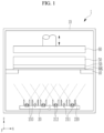
- FIG. 1 schematically illustrates a deposition apparatus according to an embodiment
- FIG. 2 schematically illustrates how a deposition source shown in FIG. 1 moves
- FIG. 3 schematically illustrates a state in which deposition material particles are deposited on a substrate through an opening of a mask.
- a deposition apparatus 1 may include a chamber 10, a deposition source 20, an angle limiting plate 30, a holder 40, a cool plate 50, and/or a magnet assembly 60.
- the deposition source 20, the angle limiting plate 30, the holder 40, the cool plate 50, and the magnet assembly 60 may be disposed within the chamber 10.
- the angle limiting plate 30 is not shown in FIG. 1 , but is shown in FIG. 2 .
- the chamber 10 may be a vacuum chamber, and the inside of the chamber 10 may be maintained in a vacuum atmosphere or an inert gas atmosphere such as nitrogen gas.
- the chamber 10 may be connected to a vacuum pump (not shown) to control the internal pressure.
- Depositing a deposition material on a substrate SB for manufacturing a display panel and the like may be performed in the chamber 10 of the deposition apparatus 1.
- the substrate SB may be fixed at a position (e.g., a predetermined or selectable position) inside the chamber 10.
- a mask MK may be disposed to align with the substrate SB.
- the mask MK may be detachably fixed to the holder 40 above the deposition source 20.
- the mask MK may be a fine metal mask having an opening corresponding to a pattern of a layer to be provided on the substrate SB (for example, a pattern of a light emitting layer of a display device).
- the mask MK may be an open mask having an opening corresponding to a layer (for example, a common layer of a display panel) to be provided in an area (e.g., a predetermined or selectable area) of the substrate SB.
- the deposition material may be deposited in a pattern (e.g., a predetermined or selectable pattern) on the substrate SB.
- the chamber 10 may include a carry-in/out port (not shown) for carrying the substrate SB and the mask MK in and out.
- the deposition source 20 may provide a deposition material to the substrate SB to be deposited by storing and evaporating the deposition material (for example, a light emitting layer material of a light emitting display panel).
- the deposition source 20 may inject the deposition material toward the substrate SB.
- the deposition source 20 may be a linear deposition source.
- the deposition source 20 may have a length in the first direction x and a width in the second direction y, and the length may be greater than the width.
- the deposition source 20 may include nozzles 210 for spraying the deposition material.
- the nozzles 210 may be disposed in a line in the first direction x on an upper portion of the deposition source 20.
- the nozzles 210 may be disposed in columns in the first direction x.
- the nozzle 210 may include a first nozzle hole 211 and/or a second nozzle hole 212, or may include a first nozzle hole 211.
- the deposition source 20 may include angle controlling structures 220 surrounding the nozzles 210.
- the angle controlling structure 220 may have a rolled plate shape or, for example, a cylindrical shape.
- the angle controlling structure 220 may have a circular planar shape.
- An angle controlling structure 220 may surround a nozzle 210.
- An angle controlling structure 220 may surround a first nozzle hole 211 and one or more second nozzle holes 212, or may surround a first nozzle hole 211.
- the angle controlling structures 220 may control an incident angle of a deposition material so that the incident angle of the deposition material sprayed from the nozzles 210 to be directed to the substrate SB through the opening of the mask MK is an angle (e.g., a predetermined or selectable angle) or more.
- the angle controlling structure 220 may restrict particles, of which an incident angle is an angle (e.g., a predetermined or selectable angle) or less, from reaching the mask MK and the substrate SB.
- the angle controlling structure 220 may restrict particles, of which an incident angle is an angle (e.g., a predetermined or selectable angle) or less, from reaching the mask MK and the substrate SB.
- the incident angle may be increased by improving the spray angle of the nozzle by improving the shape of the nozzle, but since the particle density around the nozzle is high, it may be difficult to increase the incident angle to an angle (e.g., a predetermined or selectable angle) or more only by improving the nozzle shape.
- an angle e.g., a predetermined or selectable angle
- by disposing the angle controlling structure 220 surrounding the nozzle 210 to block particles sprayed from the nozzle 210 at a low incident angle it is possible to increase the incident angle.
- a detailed configuration of the angle controlling structure 220 will be described below.
- the angle limiting plate 30 may be disposed long in the first direction x at a side and another side along a row of the nozzles 210.
- the angle limiting plate 30 can be disposed to be perpendicular to an x-y plane.
- the angle limiting plate 30 may limit the spraying direction of the deposition material sprayed from the nozzles 210.
- the angle limiting plate 30 may limit movement of deposition material particles having a relatively low incident angle.
- the magnet assembly 60 may be disposed above the substrate SB.
- the magnet assembly 60 may include magnets (not shown) and a yoke plate (not shown) supporting the magnets.
- the mask MK may be pulled toward the magnet assembly 60 by the magnetic force of the magnets of the magnet assembly 60, so the mask MK may be attached to and closely contact the substrate SB. Accordingly, it is possible to reduce a lifting phenomenon between the mask MK and the substrate SB, and to reduce a shadow effect during the deposition process.
- the magnet assembly 60 may be provided to move in a third direction z, and the deposition apparatus 1 may include an actuator for moving the magnet assembly 60 in one or more directions.
- the cool plate 50 may be disposed between the substrate SB and the magnet assembly 60 to pressurize the substrate SB with its own weight, and a close contacting degree between the substrate SB and the mask MK may be improved.
- the cool plate 50 may be non-magnetic so as to not affect magnetism of the magnet assembly 60.
- FIG. 2 briefly illustrates a relationship between the substrate SB and the deposition source 20 disposed in the chamber 10 of the deposition apparatus 1.
- the substrate SB may be disposed above the deposition source 20 to be spaced apart away from the deposition source 20.
- a surface of the substrate SB (for example, a surface on which the deposition material is deposited) may face the deposition source 20.
- the substrate SB may include two sides extending in the first direction x and two sides extending in the second direction y.
- the substrate SB may have a substantially quadrangular planar shape.
- the deposition source 20 may be disposed so as to extend in the first direction x, for example, so that a length direction of the deposition source 20 is parallel to the first direction x.
- the deposition source 20 may move in the second direction y.
- the deposition material may be provided on a surface of the substrate SB.
- the deposition source 20 may provide deposition materials containing different materials to the substrate SB. Uniform mixing of the deposition materials may improve characteristics such as color coordinates, light efficiency, a driving voltage, and a lifespan of the display device.
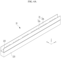
- FIG. 4A illustrates a schematic perspective view of a state in which an angle limiting plate is coupled to a deposition source according to an embodiment
- FIG. 4B illustrates a schematic perspective view of a deposition source according to an embodiment
- FIG. 4C illustrates a schematic perspective view of a state in which an angle controlling structure is separated from a deposition source according to an embodiment
- FIG. 5 illustrates a schematic plan view of the deposition source shown in FIG. 4A
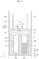
- FIG. 6 illustrates a schematic cross-sectional view taken along line A-A' of FIG. 5
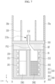
- FIG. 7 illustrates a schematic cross-sectional view taken along line B-B' of FIG. 5 .
- the deposition source 20 may include the nozzles 210, the angle controlling structures 220, a main body 230, a cover 240, a container or crucible (hereinafter referred to as "crucible") 250, a heater 260, and/or a reflector RF.
- crucible container or crucible
- the main body 230 and the cover 240 may configure an overall appearance of the deposition source 20.
- the main body 230 and the cover 240 may extend in the first direction x.
- the cover 240 may be coupled to an upper portion of the main body 230.
- the cover 240 may be separable from the main body 230.
- the main body 230 and the cover 240 may be combined to define an inner space of the deposition source 20.
- the nozzles 210 may be disposed to protrude from the cover 240 (e.g. in a direction away from an inner space of the deposition source 20).
- the nozzles 210 may be separately manufactured from the cover 240 to be coupled to the cover 240.
- the nozzles 210 may be integral with the cover 240.
- the nozzles 210 may be disposed in the first direction x.
- a distance between adjacent nozzles 210 may or may not be constant. For example, three nozzles 210 may be disposed adjacently as shown, but the distance between the nozzles 210 may be variously changed. Eighteen nozzles 210 are shown, but the number of the nozzles 210 may be variously changed.
- the nozzles 210 may include first nozzles 210a including the first nozzle hole 211 and the second nozzle hole 212 and second nozzles 210b including the first nozzle hole 211 and not including the second nozzle hole 212.
- the first nozzle 210a may be a nozzle including both the first nozzle hole 211 and the second nozzle hole 212
- the second nozzle 210b may be a nozzle including only the first nozzle hole 211.
- the second nozzle 210b may include the second nozzle hole 212 instead of the first nozzle hole 211.
- the nozzles 210 disposed at sides (e.g., both sides) of three adjacent nozzles 210 may be the first nozzles 210a, and the nozzle 210 disposed at a center thereof may be the second nozzle 210b.
- a planar shape of the first nozzle 210a may be a substantially round rhombic shape or a substantially elliptical shape.
- a planar shape of the second nozzle 210b may be a substantially circular shape.
- the disposition of the first nozzle 210a and the second nozzle 210b may be variously changed, and the nozzles 210 may not include the second nozzle 210b.
- a first nozzle hole 211 may be disposed at a center thereof, and two second nozzle holes 212 may be disposed at sides of the first nozzle hole 211.
- the first nozzle hole 211 and the second nozzle holes 212 may be aligned in the first direction x.
- the first nozzle hole 211 and the second nozzle holes 212 may be disposed on a straight line in the first direction x.
- the number and disposition of the second nozzle holes 212 in the first nozzle 210a may be variously changed.
- a first deposition material DM1 may be sprayed through the first nozzle hole 211, and a second deposition material DM2 may be sprayed through the second nozzle hole 212.
- the first deposition material DM1 and the second deposition material DM2 may be different materials.
- the first deposition material DM1 may be a host
- the second deposition material DM2 may be a guest (e.g. dopant).
- the second nozzle hole 212 may be disposed to be substantially close to the first nozzle hole 211, and for example, a distance between an upper end of the first nozzle hole 211 and an upper end of the second nozzle hole 212 may be smaller than or substantially equal to a width (for example, an inner diameter) of the second nozzle hole 212.
- the distance between the upper end of the first nozzle hole 211 and the upper end of the second nozzle hole 212 may be substantially zero. Accordingly, the mixing ratio of the first deposition material DM1 sprayed through the first nozzle hole 211 and the second deposition material DM2 sprayed through the second nozzle hole 212 may be improved, and the first deposition material DM1 and the second deposition material DM2 may be entirely deposited with the improved mixing rate on the substrate SB.
- the first nozzle hole 211 may have a "Y"-shaped cross-sectional shape (e.g. in a cross-sectional plane intersecting the first direction x), and the second nozzle hole 212 may have an "I"-shaped cross-sectional shape (e.g. in a cross-sectional plane intersecting the first direction x).
- the "Y"-shaped nozzle hole may have a three-dimensional shape having a constant width in the third direction z and then gradually widening, similar to a funnel.
- the "I"-shaped nozzle hole may have a cylinder shape with a constant width in the third direction z (i.e. shaped like a capital letter "I” without serifs).
- the "Y"-shaped nozzle hole may be more advantageous than the "I"-shaped nozzle hole in realizing a high incident angle of the deposition material.
- a cross-section of at least one of the first nozzle hole 211 and the second nozzle hole 212 has a "Y" shape
- an upper end of the first nozzle hole 211 and an upper end of the second nozzle hole 212 may substantially directly contact each other.
- the cross-sectional shapes or dimensions of the first and second nozzle holes 211 and 212 may be variously changed according to the type and the spray amount of the deposition material.
- the angle controlling structures 220 may be disposed to protrude from the cover 240 (e.g. in a direction away from an inner space of the deposition source 20) while surrounding the nozzles 210.
- An angle controlling structure 220 may surround a nozzle 210.
- the number of the angle controlling structures 220 may correspond 1:1 to the number of the nozzles 210.
- the number of the angle controlling structures 220 may not correspond to the number of the nozzles 210.
- at least some of the first nozzles 210a and/or at least some of the second nozzles 210b may not be surrounded by the angle controlling structure 220.
- the angle controlling structure 220 may completely surround a side surface of the nozzle 210.
- a center of the angle controlling structure 220 and a center of the nozzle 210 and/or the first nozzle hole 211 may be substantially the same.
- a height of the angle controlling structure 220 may be higher than that of the nozzle 210.
- an angle ⁇ formed by a center of an upper end of the nozzle 210 and an upper end of the angle controlling structure 220 (hereinafter referred to as an exit angle) may be about 40° or more, or about 60° to about 80°.
- the angle controlling structure 220 may have a cylindrical or barrel shape, but may have various three-dimensional shapes with an empty interior such as an elliptical columnar shape and a prismatic shape.
- the angle controlling structure 220 can be disposed to be perpendicular to the x-y plane.
- the angle controlling structures 220 may be separately manufactured from the cover 240 and may be coupled to the cover 240.
- the angle controlling structures 220 may be integral with the cover 240.
- the angle controlling structures 220 may be disposed at intervals corresponding to intervals between the nozzles 210. For example, three angle controlling structures 220 may be disposed adjacently as shown. Although 18 angle controlling structures 220 are shown, the number of the angle controlling structures 220 may correspond to the number of the nozzles 210.
- the angle controlling structure 220 surrounding the first nozzle 210a and the angle controlling structure 220 surrounding the second nozzle 210b may have substantially a same shape, but may have different shapes in other embodiments.
- the angle controlling structures 220 may be designed to be able to be cooled or heated.
- Particles of the first and second deposition materials DM1 and DM2 may be sprayed from the first and second nozzle holes 211 and 212 of the first nozzle 210a at a spray angle (e.g., a predetermined or selectable spray angle).
- Particles of the first deposition material DM1 may be sprayed from the first nozzle hole 211 of the second nozzle 210b at a spray angle (e.g., a predetermined or selectable spray angle).
- the angle controlling structure 220 may limit, among the particles sprayed from the nozzle 210, movement of particles sprayed at an angle (e.g., a predetermined or selectable angle) or less.
- the angle (e.g., a predetermined or selectable angle) may correspond to the exit angle ⁇ .
- the particles sprayed at the angle (e.g., a predetermined or selectable angle) or less may be blocked by the angle controlling structure 220 and may not substantially move outside the angle controlling structure 220. Accordingly, only particles having a greater incident angle than particles filtered by the angle controlling structure 220 may pass above the angle controlling structure 220 to be deposited on the substrate SB. Therefore, the shadow area may be reduced because the particles with a high incident angle substantially greater than the exit angle ⁇ may be deposited on the substrate SB.
- the particles filtered by the angle controlling structure 220 may be deposited on the angle controlling structure 220.
- the angle controlling structure 220 may have a mesh shape.
- the angle controlling structure 220 may be provided to have a wire mesh such as a woven wire mesh or a welded wire mesh.
- the angle controlling structure 220 may have a mesh shape as a whole, or only an inner surface thereof (for example, a surface facing the nozzle 210) may have a mesh shape.
- the angle controlling structure 220 may have a structure in which a metal wire mesh is provided on an inner surface of a cylindrical metal plate.
- the crucible 250 may be disposed inside the main body 230.
- the crucible 250 may include a first crucible 251 and a second crucible 252.
- the first crucible 251 and the second crucible 252 may each extend in the first direction x.
- the first crucible 251 and the second crucible 252 may be spaced apart from each other in the second direction y.
- a volume of the first crucible 251 and a volume of the second crucible 252 may be the same, but may be different in other embodiments.
- the first crucible 251 may accommodate the first deposition material DM1
- the second crucible 252 may accommodate the second deposition material DM2.
- the first deposition material DM1 may be a host material
- the second deposition material DM2 may be a dopant material.
- the first crucible 251 may be connected in fluid communication with the first nozzle hole 211 through a first passage PS1, and the second crucible 252 may be connected in fluid communication with the second nozzle hole 212 through a second passage PS2. Accordingly, the first deposition material DM1 in the first crucible 251 may be sprayed out of the deposition source 20 through the first passage PS1 and the first nozzle hole 211, and the second deposition material DM2 in the second crucible 252 may be sprayed out of the deposition source 20 through the second passage PS2 and the second nozzle hole 212.
- the first passage PS1 may be a tube, a hole formed in a structure disposed between the first crucible 251 and the first nozzle hole 211, or a combination of a tube and a hole.
- the second passage PS2 may be a tube, a hole formed in a structure disposed between the second crucible 252 and the second nozzle hole 212, or a combination of a tube and a hole.
- first deposition material DM1 and the second deposition material DM2 are mixed inside the deposition source 20
- a reverse flow of one of the first and second deposition materials DM1 and DM2 may occur due to a vaporization temperature difference between the first deposition material DM1 and the second deposition material DM2.
- the first deposition material DM1 and the second deposition material DM2 are not mixed inside the deposition source 20 and may be sprayed outside the deposition source 20 through their respective channels, so that the problem such as the reverse flow of the first or second deposition material DM1 or DM2 may not occur.
- the heater 260 may be disposed within the main body 230 to heat the crucible 250.
- the heater 260 may include a first heater 261 and a second heater 262.
- the first heater 261 may heat the first crucible 251 to evaporate the first deposition material DM1 in the first crucible 251.
- the second heater 262 may heat the second crucible 252 to evaporate the second deposition material DM2 in the second crucible 252.
- the first heater 261 may be disposed between an inner wall of the main body 230 and the first crucible 251, and the second heater 262 may be disposed between the inner wall of the main body 230 and the second crucible 252, but the position of the heater 260 may be variously changed.
- the first heater 261 may be disposed on a side surface of the first crucible 251 and/or under the first crucible 251, and the second heater 262 may be disposed on a side surface of the second crucible 252 and/or under the second crucible 252.
- the first heater 261 and the second heater 262 may independently operate.
- an amount of heat energy applied to the first crucible 251 by the first heater 261 may be different from an amount of heat energy applied to the second crucible 252 by the second heater 262.
- the first crucible 251 and the second crucible 252 may be heated at different temperatures, and an internal temperature of the first crucible 251 and an internal temperature of the second crucible 252 may be different.
- An insulating wall IN surrounding the first crucible 251 and the second crucible 252 may be disposed inside the main body 230.
- the insulating wall IN may prevent heat inside the main body 230 from leaking out of the main body 230. Accordingly, it is possible to suppress heat generated from the deposition source 20 from being dissipated into the chamber 10, and to prevent heat from affecting the substrate SB or damaging structures inside the chamber 10.
- the insulating wall IN may be disposed between the first crucible 251 and the second crucible 252 to block thermal exchange between the first crucible 251 and the second crucible 252. Accordingly, temperatures of the first crucible 251 and the second crucible 252 may be readily independently controlled.
- a reflector RF may be disposed between the nozzle 210 and the crucible 250.
- the reflector RF may include an insulating material.
- the reflector RF may prevent heat from the first crucible 251 and the second crucible 252 from leaking in an upper direction of the main body 230. Accordingly, the reflector RF may block heat from the deposition source 20 leaking toward the substrate SB.
- the reflector RF may be disposed on the cover 240, or the cover 240 may function as the reflector RF.
- the angle limiting plate 30 may be disposed on the deposition source 20. A lower end portion of the angle limiting plate 30 may contact the deposition source 20.
- the angle limiting plate 30 may be disposed on the cover 240 and the lower end portion thereof may contact the cover 240.
- the angle limiting plate 30 may be combined with the cover 240 or integral with the cover 240.
- the angle limiting plate 30 may include a first angle limiting plate 30a and a second angle limiting plate 30b respectively disposed at a side and another side of the nozzles 210.
- the first and second angle limiting plates 30a and 30b may be disposed long in the first direction x along the row of the nozzles 210.
- the first and second angle limiting plates 30a and 30b may be disposed to be spaced apart from each other with the nozzles 210 and the angle controlling structures 220 therebetween in the second direction y.
- a height of the angle limiting plate 30 may be higher than that of the nozzles 210 and/or that of the angle controlling structures 220 (e.g. higher than that of the nozzles 210 and that of the angle controlling structures 220).
- the angle limiting plate 30 may limit sprayed directions of the first and second deposition materials DM1 and DM2 sprayed from the first and second nozzle holes 211 and 212 of the nozzles 210. Accordingly, it is possible to reduce an amount of waste deposition material that is not deposited on the substrate SB.
- FIG. 8 illustrates a graph of shadow effects in deposition apparatuses according to a comparative example and examples.
- a horizontal axis in the graph may represent a position of a substrate, and a vertical axis may represent a width of a shadow area.
- Example 1-1 and Example 1-2 illustrate the widths of the shadow areas during deposition using the deposition source 20 shown in FIG. 5 , and Example 1-1 and Example 1-2 respectively may be cases in which the exit angles ⁇ are about 52° and about 50°.
- the comparative example illustrates the width of the shadow area during deposition using a deposition source not including the angle controlling structure 220 in the deposition source 20 shown in FIG. 5 .
- the width of the shadow area ranged from about 2.0 ⁇ m to about 2.9 ⁇ m according to the position of the substrate.
- the width of the shadow area ranged from about 3.4 ⁇ m to about 4.7 ⁇ m according to the position of the substrate.
- the width of the shadow area was significantly reduced compared to the comparative example.
- a difference between a minimum value and a maximum value of the shadow area according to the position of the substrate was about 1.3 ⁇ m in the comparative example, but was about 0.9 ⁇ m, as an improved value, in Example 1-1 and Example 1-2.
- material efficiencies (%) calculated as (deposition amount/evaporation amount) x 100 were about 51.0 %, about 49.2 %, and about 50.4 %, in the comparative example, Example 1-1, and Example 1-2, respectively. It can be seen that the material efficiency was not significantly reduced compared to the case of using the deposition source not including the angle controlling structure 220, even though the angle controlling structure 220 was used to limit low incident angle particles. As described above, the deposition source 20 including the angle controlling structure 220 according to the embodiment may reduce a shadow effect without substantially reducing material efficiency.
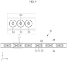
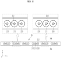
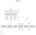
- FIG. 9 , FIG. 10 , FIG. 11 , and FIG. 12 each illustrate a schematic plan view of a deposition source according to an embodiment.
- FIG. 9 , FIG. 10 , FIG. 11 , and FIG. 12 may be different from the embodiment shown in FIG. 5 in the disposition of the second nozzle hole 212.
- the deposition source 20 may include the nozzles 210 disposed in the first direction x, and may include the angle controlling structures 220 surrounding the nozzles 210.
- An angle controlling structure 220 may surround a nozzle 210.
- the nozzle 210 may have a planar shape of an approximately water-drop shape in which an approximately semicircular shape and an approximately semi-elliptical shape are combined.
- the nozzle 210 may include the first nozzle hole 211 and the second nozzle hole 212.
- the second nozzle hole 212 may be disposed in front of the first nozzle hole 211 (e.g.
- the respective first nozzle hole 211 and the respective second nozzle hole 212 may be disposed on a straight line in the second direction y), for example, to be directed to the second direction y, which may be a movement direction of the deposition source 20 during deposition.
- a distance between the upper end of the first nozzle hole 211 and the upper end of the second nozzle hole 212 in the second direction y may be less than or substantially equal to the width of the second nozzle hole 212, for example, substantially zero.
- the upper end of the first nozzle hole 211 and the upper end of the second nozzle hole 212 may substantially directly contact each other.
- the first nozzle holes 211 may be aligned in the first direction x
- the second nozzle holes 212 may be aligned in the first direction x
- the first nozzle holes 211 and the second nozzle holes 212 may be aligned side by side in the first direction x.
- a line connecting the centers of the first nozzle holes 211 and a line connecting the centers of the second nozzle holes 212 in the first direction x may be side by side and may be spaced apart from each other by a distance between the centers of the adjacent first and second nozzle holes 211 and 212.
- respective nozzles 210 are illustrated as including the first nozzle hole 211 and the second nozzle hole 212, some nozzles may include only the first nozzle hole 211 or only the second nozzle hole 212.
- the deposition source 20 may include the nozzles 210 disposed in the first direction x, and may include the angle controlling structures 220 surrounding the nozzles 210.
- An angle controlling structure 220 may surround a nozzle 210.
- the nozzle 210 may have a planar shape of an approximately water-drop shape in which an approximately semicircular shape and an approximately semi-elliptical shape are combined.
- the nozzle 210 may include the first nozzle hole 211 and the second nozzle hole 212.
- the second nozzle hole 212 may be disposed at a side of the first nozzle hole 211.
- a distance between the upper end of the first nozzle hole 211 and the upper end of the second nozzle hole 212 may be less than or substantially equal to the width of the second nozzle hole 212, for example, substantially zero.
- the first nozzle holes 211 and the second nozzle holes 212 may be disposed on a straight line extending in the first direction x. In each nozzle 210, it is shown that the second nozzle hole 212 is disposed at the left side of the first nozzle hole 211, but the second nozzle hole 212 may be disposed at the right side of the first nozzle hole 211.
- respective nozzles 210 are illustrated as including the first nozzle hole 211 and the second nozzle hole 212, some nozzles may include only the first nozzle hole 211 or only the second nozzle hole 212.
- the second nozzle hole 212 in the nozzle 210 disposed at a left side may be disposed at the left side of the first nozzle hole 211
- the second nozzle hole 212 in the nozzle 210 disposed at a right side may be disposed at the right side of the first nozzle hole 211.
- the second nozzle hole 212 in the nozzle 210 disposed at the left side may be disposed at the right side of the first nozzle hole 211
- the second hole 212 in the nozzle 210 disposed at the right side may be disposed at the left side of the first nozzle hole 211.
- each nozzle 210 may include a first nozzle hole 211 and two second nozzle holes 212, and the two second nozzle holes 212 may be disposed at the sides of the first nozzle hole 211.
- the nozzle 210 may have a substantially round rhombus shape or a substantially elliptical planar shape.
- the first nozzle hole 211 and the second nozzle holes 212 may be aligned in the first direction x.
- the embodiment of FIG. 12 may differ from the embodiment of FIG. 5 at least in that all nozzles 210 include the second nozzle holes 212.
- FIG. 13 illustrates a graph of a deposition profile during deposition using deposition sources according to some embodiments.
- Example 1 may be an example of deposition using the deposition source according to the embodiment of FIG. 5
- Example 2 may be an example of deposition using the deposition source according to the embodiment of FIG. 9
- Example 3 may be an example of deposition using the deposition source according to the embodiment of FIG. 10
- Example 4 may be an example of deposition using the deposition source according to the embodiment of FIG. 11
- Example 5 may be an example of deposition using the deposition source according to the embodiment of FIG. 12 .
- deposition profiles of Example 1 and Example 2 were relatively uniform.
- Example 2 was more uniform.
- the second nozzle holes 212 were aligned with the first nozzle holes 211 in the first direction x, but in case that the second nozzle hole 212 was disposed at a side of the first nozzle hole 211, a thickness change of the deposition material was relatively large depending on the position on the substrate.
- the deposition profile was more uniform in Example 1 in which some nozzles 210 did not include the second nozzle hole 212 than in Example 5 in which all nozzles 210 included the second nozzle hole 212.
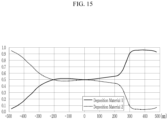
- FIG. 14 and FIG. 15 each illustrate a graph of a deposition ratio of deposition materials during deposition using a deposition source according to an embodiment.
- the horizontal axis may represent a position of the substrate relative to the deposition source, and the vertical axis may represent a deposition ratio of Deposition Material 1 and Deposition Material 2.
- Deposition Material 1 may represent the deposition material sprayed through the first nozzle hole 211
- Deposition Material 2 may represent the deposition material sprayed through the second nozzle hole 212.
- FIG. 14 illustrates a deposition ratio during deposition using the deposition source according to the embodiment of FIG. 5 (corresponding to Example 1 in FIG. 13 )
- FIG. 15 illustrates a deposition ratio during deposition using the deposition source according to the embodiment of FIG. 9 (corresponding to Example 2 in FIG. 13 ). Referring to FIG.
- Deposition Material 1 and Deposition Material 2 were deposited within a range of about 0.3 to about 0.7. Referring to FIG. 15 , Deposition Material 1 and Deposition Material 2 were deposited within a wide range of about 0.05 to about 0.95, and it was found that at first Deposition Material 1 was mainly deposited and below Deposition Material 2 was mainly deposited.
- the case of using the deposition source in which the first nozzle holes 211 and the second nozzle holes 212 are aligned in a straight line has a more uniform deposition ratio of Deposition Material 1 and Deposition Material 2 and a more uniform mixing ratio thereof accordingly than the case of using the deposition source in which the first nozzle holes 211 and the second nozzle holes 212 are adjacent but aligned side by side.
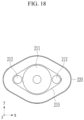
- FIG. 16 , FIG. 17 , and FIG. 18 each illustrate a schematic plan view of a nozzle and an angle controlling structure of a deposition source according to an embodiment.
- FIG. 16 illustrates a nozzle 210 and an angle controlling structure 220 surrounding a nozzle 210.
- the nozzle 210 may include the first nozzle hole 211 through which the first deposition material may be sprayed and the second nozzle hole 212 through which the second deposition material may be sprayed.
- the first nozzle hole 211 and the second nozzle hole 212 may have a "Y"-shaped cross-sectional shape (e.g. in a cross-sectional plane intersecting the first direction x).
- An upper end of the first nozzle hole 211 and an upper end of the second nozzle hole 212 may be adjacent to or substantially contact each other.
- the first nozzle hole 211 and the second nozzle hole 212 may be aligned in the first direction x.
- the planar shape of the nozzle 210 may be substantially a track shape extending in the first direction x or substantially an elliptical shape.
- the angle controlling structure 220 may have a substantially track shape or a substantially elliptical shape extending in the first direction x.
- first and second nozzle holes 211 and 212 included in a nozzle 210 are configured to have a "Y" shape, and in case that the first deposition material and the second deposition material are deposited in similar amounts, it may be advantageous to implement a high angle of incidence. Since each material to be deposited has different characteristics, control of the incident angle of the deposition materials may be optimized by changing and combining the shape of the first nozzle hole 211, the shape of the second nozzle hole 212, and the shape of the angle controlling structure 220. At least one of the nozzles 210 and the angle controlling structures 220 shown in FIG. 5 , FIG. 9 , FIG. 10 , FIG. 11 , and FIG. 12 may have the structure shown in FIG. 16 .
- FIG. 17 illustrates a nozzle 210 and an angle controlling structure 220 surrounding the nozzle 210.
- the nozzle 210 may include the first nozzle hole 211 through which the first deposition material may be sprayed and the second nozzle hole 212 through which the second deposition material may be sprayed.
- the second nozzle hole 212 having an "I"-shaped cross-sectional shape (e.g. in a cross-sectional plane intersecting the first direction x) may be disposed at a side of the first nozzle hole 211 having a "Y"-shaped cross-sectional shape (e.g. in a cross-sectional plane intersecting the first direction x).
- the first and second nozzle holes 211 and 212 may be aligned in the first direction x.
- the nozzle 210 may have a planar shape of an egg-like shape or an approximately water-drop shape in which an approximately semicircular shape and an approximately semi-elliptical shape are combined.
- the angle controlling structure 220 may have a planar shape of a substantially egg-like shape or a substantially droplet-like shape in which a semi-circular shape and a semi-elliptical shape are combined, corresponding to the planar shape of the nozzle 210.
- FIG. 18 illustrates a nozzle 210 and an angle controlling structure 220 surrounding the nozzle 210.
- the nozzle 210 may include the first nozzle hole 211 through which the first deposition material may be sprayed and the second nozzle holes 212 through which the second deposition material may be sprayed.
- the second nozzle holes 212 may be disposed at sides of the first nozzle hole 211, and the first and second nozzle holes 211 and 212 may be aligned in the first direction x.
- the first nozzle hole 211 may have a "Y"-shaped cross-sectional shape (e.g. in a cross-sectional plane intersecting the first direction x), and the second nozzle hole 212 may have an "I"-shaped cross-sectional shape (e.g.
- the nozzle 210 may have a substantially round rhombus planar shape.
- the angle controlling structure 220 may have a substantially round rhombus planar shape corresponding to the planar shape of the nozzle 210.
- the planar shape of the angle controlling structure 220 is not limited to the round shape, and may be changed in consideration of a planar shape corresponding to the planar shape of the nozzle 210. Since the characteristic is different for each material to be deposited, it is possible to optimize the control of the incident angle of the deposition materials by changing the shape of the angle controlling structure 220.
- FIG. 19 illustrates a schematic cross-sectional view of a stacked structure of a display panel according to an embodiment.
- the cross-section shown in FIG. 19 may substantially correspond to a pixel area.
- a display panel DP that may include the layers that may be provided by using the above-described deposition apparatus 1 may include a substrate SB, a transistor TR provided on the substrate SB, and/or a light emitting diode LED electrically connected to the transistor TR.
- the light emitting diode LED may correspond to a pixel.
- the substrate SB may be a flexible substrate SB capable of being bent, folded, and/or rolled.
- the substrate SB may be a single layer or a multilayer including a first base layer BL1, an inorganic layer IL, and a second base layer BL2.
- the first base layer BL1 and the second base layer BL2 may include a polymer resin such as a polyimide, a polyamide, a polyethylene terephthalate, or a combination thereof.
- a barrier layer BR that prevents impurities, e.g., moisture, oxygen, etc., from penetrating may be disposed on the substrate SB.
- the barrier layer BR may include an inorganic insulating material such as a silicon nitride (SiN x ), a silicon oxide (SiO x ), a silicon oxynitride (SiO x N y ), or a combination thereof, and may be a single layer or a multilayer.
- a buffer layer BF may be positioned on the barrier layer BR.
- the buffer layer BF may block impurities from the substrate SB in case that a semiconductor layer is provided, thereby improving characteristics of the semiconductor layer, and flattening a surface of the substrate SB to reduce stress on the semiconductor layer.
- the buffer layer BF may include an inorganic insulating material such as a silicon nitride, a silicon oxide, a silicon oxynitride, or a combination thereof, and may be a single layer or a multilayer.
- the buffer layer BF may include an amorphous silicon (a-Si).
- a semiconductor layer AL of the transistor TR may be disposed on the buffer layer BF.
- the semiconductor layer AL may include a first area, a second area, and a channel area between the first and second areas.
- the semiconductor layer AL may include at least one of amorphous silicon, polysilicon, and an oxide semiconductor.
- the oxide semiconductor may include at least one of zinc (Zn), indium (In), gallium (Ga), and tin (Sn).
- the semiconductor layer AL may include a low temperature polysilicon (LTPS) or an indium-gallium-zinc oxide (IGZO).
- a first gate insulating layer GI1 may be disposed on the semiconductor layer AL.
- the first gate insulating layer GI1 may include an inorganic insulating material such as a silicon nitride, a silicon oxide, or a silicon oxynitride, and may be a single layer or a multilayer.
- a first gate conductive layer that may include a gate electrode GE of the transistor TR, a gate line GL, and a first electrode C1 of a storage capacitor CS may be disposed on the first gate insulating layer GI1.
- the first gate conductive layer may include molybdenum (Mo), aluminium (Al), copper (Cu), titanium (Ti), the like, or a combination thereof, and may be a single layer or a multilayer.
- a second gate insulating layer GI2 may be disposed on the first gate conductive layer.
- the second gate insulating layer GI2 may include an inorganic insulating material such as a silicon nitride, a silicon oxide, or a silicon oxynitride, and may be a single layer or a multilayer.
- a second gate conductive layer that may include a second electrode C2 of the storage capacitor CS may be disposed on the second gate insulating layer GI2.
- the second gate conductive layer may include molybdenum (Mo), aluminium (Al), copper (Cu), titanium (Ti), the like, or a combination thereof, and may be a single layer or a multilayer.
- An interlayer insulating layer ILD may be disposed on the second gate insulating layer GI2 and the second gate conductive layer.
- the interlayer insulating layer ILD may include an inorganic insulating material such as a silicon nitride, a silicon oxide, or a silicon oxynitride, and may be a single layer or a multilayer.
- a first data conductive layer that may include a first electrode SE and a second electrode DE of the transistor TR, and a data line DL may be disposed on the interlayer insulating layer ILD.
- the first electrode SE and the second electrode DE may be respectively electrically connected to the first region and the second region of the semiconductor layer AL through contact holes of the insulating layers GI1, GI2, and ILD.
- At least one of the first electrode SE and the second electrode DE may be a source electrode, and the other thereof may be a drain electrode.
- the first data conductive layer may include aluminium (Al), platinum (Pt), palladium (Pd), silver (Ag), magnesium (Mg), gold (Au), nickel (Ni), neodymium (Nd), iridium (Ir), chromium (Cr), calcium (Ca), molybdenum (Mo), titanium (Ti), tungsten (W), copper (Cu), or a combination thereof, and may be a single layer or a multilayer.
- a first planarization layer VIA1 may be disposed on the first data conductive layer.
- the first planarization layer VIA1 may include an organic insulating material such as a general purpose polymer such as poly(methyl methacrylate) and polystyrene, a polymer derivative having a phenol-based group, an acryl-based polymer, an imide-based polymer (for example, a polyimide), a siloxane-based polymer, or a combination thereof.
- a second data conductive layer that may include a voltage line VL, a connection member CM, and the like, may be disposed on the first planarization layer VIA1.
- the voltage line VL may transmit a voltage such as a driving voltage, a common voltage, an initialization voltage, or a reference voltage.
- the connection member CM may be electrically connected to the second electrode DE of the transistor TR through a contact hole of the first planarization layer VIA1.
- the second data conductive layer may include aluminium (Al), platinum (Pt), palladium (Pd), silver (Ag), magnesium (Mg), gold (Au), nickel (Ni), neodymium (Nd), iridium (Ir), chromium (Cr), calcium (Ca), molybdenum (Mo), titanium (Ti), tungsten (W), copper (Cu), or a combination thereof, and may be a single layer or a multilayer.
- a second planarization layer VIA2 may be disposed on the second data conductive layer.
- the second planarization layer VIA2 may include an organic insulating material such as a general purpose polymer such as polymethylmethacrylate and polystyrene, a polymer derivative having a phenol-based group, an acryl-based polymer, an imide-based polymer, a siloxane-based polymer, or a combination thereof.
- a first electrode E1 of the light emitting diode LED may be disposed on the second planarization layer VIA2.
- the first electrode E1 may be referred to as a pixel electrode.
- the first electrode E1 may be electrically connected to the connection member CM through a contact hole of the second planarization layer VIA2. Therefore, the first electrode E1 may be electrically connected to the second electrode DE of the transistor TR to receive a driving current that controls luminance of the light emitting diode LED.
- the transistor TR to which the first electrode E1 is electrically connected may be a driving transistor, or a transistor electrically connected to the driving transistor.
- the first electrode E1 may be made of a reflective conductive material or a translucent conductive material, or it may be made of a transparent conductive material.
- the first electrode E1 may include a transparent conductive material such as an indium tin oxide (ITO) or an indium zinc oxide (IZO).
- the first electrode E1 may include a metal such as lithium (Li), calcium (Ca), aluminium (Al), silver (Ag), magnesium (Mg), or gold (Au), or a metal alloy thereof.
- a pixel defining layer PDL may be disposed on the second planarization layer VIA2 and the first electrode E1.
- the pixel defining layer PDL may be referred to as a bank or a partition wall, and may have an opening overlapping the first electrode E1.
- the pixel defining layer PDL may include an organic insulating material such as a general purpose polymer such as poly(methyl methacrylate) and polystyrene, a polymer derivative having a phenol-based group, an acryl-based polymer, an imide-based polymer, a siloxane-based polymer, or a combination thereof.
- a spacer SP may be disposed on the pixel defining layer PDL.
- the spacer SP may include an organic insulating material such as an acryl-based polymer, an imide-based polymer, or an amide-based polymer.
- a light emitting layer EL of the light emitting diode LED may be disposed on the first electrode E1.
- the light emitting layer EL may be provided by using the aforementioned deposition apparatus.
- a functional layer including at least one of a hole injection layer, a hole transport layer, an electron transport layer, and an electron injection layer may be disposed on the first electrode E1 in addition to the light emitting layer EL.
- the functional layer may be a common layer of the display panel DP, and may be provided by using the aforementioned deposition apparatus.
- a second electrode E2 of the light emitting diode LED may be disposed on the light emitting layer EL.
- the second electrode E2 may be referred to as a common electrode.
- the second electrode E2 may have a light transmittance by forming a thin layer of a metal or a metal alloy having a low work function such as calcium (Ca), barium (Ba), magnesium (Mg), aluminium (Al), silver (Ag), the like, or a combination thereof.
- the second electrode E2 may include a transparent conductive oxide such as an indium tin oxide (ITO) or an indium zinc oxide (IZO).
- the second electrode E2 may be a common layer of the display panel DP, and may be provided by using the aforementioned deposition apparatus.
- the first electrode E1, the light emitting layer EL, and the second electrode E2 of each pixel may configure the light emitting diode LED such as an organic light emitting diode.
- the first electrode E1 may be an anode
- the second electrode E2 may be a cathode.
- a light emitting area of the light emitting diode LED may correspond to a pixel.
- a capping layer CPL may be disposed on the second electrode E2.
- the capping layer CPL may improve light efficiency through refractive index adjustment.
- the capping layer CPL may be disposed to entirely cover the second electrode E2.
- the capping layer CPL may include an organic insulating material or an inorganic insulating material.
- An encapsulation layer EN may be disposed on the capping layer CPL.
- the encapsulation layer EN may encapsulate the light emitting diode LED to prevent moisture or oxygen from penetrating from the outside.
- the encapsulation layer EN may be a thin film encapsulation layer in which an organic layer EOL is disposed between a first inorganic layer EIL1 and a second inorganic layer EIL2.
- a touch sensor layer TS including touch electrodes may be disposed on the encapsulation layer EN.
- An anti-reflective layer AR for reducing reflection of external light may be disposed on the touch sensor layer TS.
- a protective film PF may be disposed under the substrate SB.
- the protective film PF may protect the display panel DP in the manufacturing process of the display device.
- the protective film PF may include a polymer such as a polyethylene terephthalate, a silicon-based polymer (for example, polydimethylsiloxane), an elastomer (for example, elastomeric polyurethane), or a combination thereof.
Landscapes
- Chemical & Material Sciences (AREA)
- Engineering & Computer Science (AREA)
- Chemical Kinetics & Catalysis (AREA)
- Materials Engineering (AREA)
- Mechanical Engineering (AREA)
- Metallurgy (AREA)
- Organic Chemistry (AREA)
- General Chemical & Material Sciences (AREA)
- Manufacturing & Machinery (AREA)
- Physical Vapour Deposition (AREA)
Abstract
Description
- This disclosure relates to a deposition apparatus, and more specifically, to a deposition apparatus that may evenly mix and deposit deposition materials and provide a high angle of incidence.
- A light emitting display device is used as device for displaying an image. The light emitting display device may include a display panel providing a screen displaying an image. The light emitting display device may display an image by a combination of pixels, and the pixel may be realized by a light emitting element such as a light emitting diode.
- The light emitting diode may include an anode, a cathode, and a light emitting layer therebetween. The light emitting layer of the light emitting diode may be provided by a deposition method. For example, by disposing a substrate on which light emitting layers are to be provided on a mask in which openings of a pattern are provided in a vacuum chamber, and then passing a material of the light emitting layers through the openings of the mask, the light emitting layers matching the pattern may be deposited on the substrate.
- The material of the light emitting layers may be vaporized from a deposition source and discharged from a nozzle to pass through the opening of the mask. In this case, particles of the material may be deposited on the substrate at a constant angle while moving in a straight line at the discharge angle. In case that the particles pass through the opening of the mask, a portion in which they are not evenly deposited (for example, they are not deposited to be uniformly thick) on the substrate (that is, a portion with a non-uniform thickness) may occur due to an angle of incidence of the particles. This portion may be referred to as a shadow.
- The above information disclosed in this Background section is only for enhancement of understanding of the background of the disclosure, and therefore it may contain information that does not form the prior art that is already known in this country to a person of ordinary skill in the art.
- In order to improve a lifespan of the light emitting element, it may be advantageous for the deposition materials to be evenly mixed and deposited. In addition, in order to increase resolution of the display device and increase efficiency of the light emitting element, it may be advantageous to reduce the shadow area by increasing the incident angle of the deposition material. Embodiments are to provide a deposition apparatus that may increase a mixing rate and an incident angle of a deposition material deposited on a substrate.
- The technical objectives to be achieved by the disclosure are not limited to those described herein, and other technical objectives that are not mentioned herein would be clearly understood by a person skilled in the art from the description of the disclosure.
- An embodiment provides a deposition apparatus including a chamber; and a deposition source disposed in the chamber and including a plurality of nozzles arranged in a first direction. Each of the plurality of nozzles includes at least one first nozzle including a first nozzle hole configured to spray (e.g. spraying) a first deposition material and a second nozzle hole configured to spray (e.g. spraying) a second deposition material, and the deposition source further includes at least one angle controlling structure surrounding the at least one first nozzle.
- The first nozzle hole and the second nozzle hole may be arranged on a same line in the first direction.
- The at least one first nozzle may include one first nozzle hole and two second nozzle holes disposed on both sides of the first nozzle (e.g. two second nozzle holes, wherein a second nozzle hole is disposed on one side of the first nozzle, and another second nozzle hole is disposed on another side of the first nozzle), and the first and second nozzle holes may be disposed on the same line in the first direction.
- The at least one first nozzle may have a round rhombic planar shape.
- The first nozzle hole may have a "Y" cross-sectional shape, and the second nozzle hole may have an "I" cross-sectional shape.
- A height of the at least one angle controlling structure may be higher than a height of the at least one first nozzle.
- An angle formed by a center of an upper end of the at least one first nozzle and an upper end of the at least one angle controlling structure with respect to a horizontal plane may be about 40° or more.
- The at least one angle controlling structure may be cylindrical.
- The at least one angle controlling structure may have a planar shape of a track shape, an elliptical shape, an egg-like shape, a water drop-like shape, or a round rhombic shape.
- The deposition source may further include a first container configured to accommodate (e.g. accommodating) the first deposition material and a second container configured to accommodate (e.g. accommodating) the second deposition material. The first nozzle hole may be connected in fluid communication with the first container through a first passage, and the second nozzle hole may be connected in fluid communication with the second container through a second passage.
- The plurality of nozzles may further include at least one second nozzle including a first nozzle hole configured to spray (e.g. spraying) the first deposition material and not including a second nozzle hole configured to spray (e.g. spraying) the second deposition material. At least part of the at least one angle controlling structure surrounds the second nozzle.
- The at least one first nozzle includes a plurality of first nozzles, the at least one second nozzle may include a plurality of second nozzles, and the at least one angle controlling structure may include a plurality of angle controlling structures, a number of the at least one of angle controlling structures corresponding to a number of the at least one first and second nozzles. In three adjacent nozzles included in the plurality of nozzles, two nozzles disposed at both sides (e.g. of the three adjacent nozzles) may be the plurality of first nozzles and one nozzle disposed in a center (e.g. of the three adjacent nozzles) may be the at least one second nozzle.
- The deposition apparatus may further include an angle limiting plate disposed on the deposition source and extending in the first direction. The angle limiting plate may include a first angle limiting plate and a second angle limiting plate respectively disposed at one side and the other side of the plurality of nozzles in a second direction crossing the first direction.
- The at least one first nozzle may include a plurality of first nozzles, and a plurality of first nozzle holes and a plurality of second nozzle holes included in the plurality of first nozzles may be arranged side by side in the first direction.
- A distance between an upper end of the first nozzle hole and an upper end of the second nozzle hole may be smaller than or substantially equal to a width of the second nozzle hole.
- Another embodiment provides a deposition apparatus including a chamber in which a substrate and a mask are disposed to be aligned; and a deposition source disposed in the chamber and configured to provide (e.g. providing) deposition material to the substrate. The deposition source may include a plurality of nozzles arranged in a first direction and respectively including a first nozzle hole and a second nozzle hole adjacent to each other, and at least one angle controlling structure individually surrounding the plurality of nozzles.
- The first nozzle hole and the second nozzle hole may be aligned in the first direction.
- Each of the at least one angle controlling structure(s) may have a cylindrical three-dimensional shape.
- A center of the at least one angle controlling structure may be a same as a center of the nozzle or a center of the first nozzle hole.
- The deposition source may include a first container configured to accommodate (e.g. accommodating) a first deposition material; and a second container configured to accommodate (e.g. accommodating) a second deposition material. The first nozzle hole may be connected in fluid communication with the first container, and the second nozzle hole may be connected in fluid communication with the second container.
- At least some of the above and other features of the invention are set out in the claims.
- According to the embodiments, it is possible to provide a deposition apparatus that may increase a mixing rate and an incident angle of deposition materials deposited on a substrate. Further, according to the embodiments, there is an advantageous effect that may be recognized throughout the present specification.
-
-
FIG. 1 schematically illustrates a deposition apparatus according to an embodiment. -
FIG. 2 schematically illustrates how a deposition source shown inFIG. 1 moves. -
FIG. 3 schematically illustrates a state in which deposition material particles are deposited on a substrate through an opening of a mask. -
FIG. 4A illustrates a perspective view of a state in which an angle limiting plate is coupled to a deposition source according to an embodiment,FIG. 4B illustrates a perspective view of a deposition source according to an embodiment, andFIG. 4C illustrates a perspective view of a state in which an angle controlling structure is separated from a deposition source according to an embodiment. -
FIG. 5 illustrates a schematic plan view of the deposition source shown inFIG. 4A . -
FIG. 6 illustrates a schematic cross-sectional view taken along line A-A' ofFIG. 5 . -
FIG. 7 illustrates a schematic cross-sectional view taken along line B-B' ofFIG. 5 . -
FIG. 8 illustrates a graph of shadow effects in deposition apparatuses according to a comparative example and examples. -
FIG. 9 ,FIG. 10 ,FIG. 11 , andFIG. 12 each illustrate a schematic plan view of a deposition source according to an embodiment. -
FIG. 13 illustrates a graph of a deposition profile during deposition using deposition sources according to some embodiments. -
FIG. 14 andFIG. 15 each illustrate a graph of a deposition ratio of deposition materials during deposition using a deposition source according to an embodiment. -
FIG. 16 ,FIG. 17 , andFIG. 18 each illustrate a schematic plan view of a nozzle and an angle controlling structure of a deposition source according to an embodiment. -
FIG. 19 illustrates a schematic cross-sectional view of a stacked structure of a display panel according to an embodiment. - This disclosure will be described more fully hereinafter with reference to the accompanying drawings, in which embodiments are shown.
- A size and thickness of each element illustrated in the drawings are arbitrarily shown for ease of description.
- It will be understood that when an element such as a layer, film, area, region, or substrate is referred to as being "on" or "above" another element, it can be directly on the other element or intervening elements may also be present. In contrast, when an element is referred to as being "directly on" another element, there are no intervening elements present.
- Throughout this specification, unless explicitly described to the contrary, the word "comprise" and variations such as "comprises" or "comprising" will be understood to imply the inclusion of stated elements but not the exclusion of any other elements.
- When an element is referred to as being "on," "connected to," or "coupled to" another element, it may be directly on, connected to, or coupled to the other element or intervening elements or layers may be present. When, however, an element is referred to as being "directly on," "directly connected to," or "directly coupled to" another element, there are no intervening elements or layers present. To this end, the term "connected" may refer to physical, electrical, and/or fluid connection, with or without intervening elements. It may also be understood that if one part and another part are connected, they may or may not be integral with each other.
- In the drawings, as symbols x, y, and z used for indicating directions, 'x' is a first direction, 'y' is a second direction perpendicular to the first direction, and 'z' is a third direction perpendicular to the first direction and the second direction.
- The term "and/or" includes all combinations of one or more of which associated configurations may define. For example, "A and/or B" may be understood to mean "A, B, or A and B."
- For the purposes of this disclosure, the phrase "at least one of A and B" may be construed as A only, B only, or any combination of A and B. Also, "at least one of X, Y, and Z" and "at least one selected from the group consisting of X, Y, and Z" may be construed as X only, Y only, Z only, or any combination of two or more of X, Y, and Z.
- Unless otherwise defined or implied herein, all terms (including technical and scientific terms) used herein have the same meaning as commonly understood by those skilled in the art to which this disclosure pertains. It will be further understood that terms, such as those defined in commonly used dictionaries, should be interpreted as having a meaning that is consistent with their meaning in the context of the relevant art and the disclosure, and should not be interpreted in an ideal or excessively formal sense unless clearly so defined herein.
-
FIG. 1 schematically illustrates a deposition apparatus according to an embodiment, andFIG. 2 schematically illustrates how a deposition source shown inFIG. 1 moves.FIG. 3 schematically illustrates a state in which deposition material particles are deposited on a substrate through an opening of a mask. - Referring to
FIG. 1 andFIG. 2 , adeposition apparatus 1 according to an embodiment may include achamber 10, adeposition source 20, anangle limiting plate 30, aholder 40, acool plate 50, and/or amagnet assembly 60. Thedeposition source 20, theangle limiting plate 30, theholder 40, thecool plate 50, and themagnet assembly 60 may be disposed within thechamber 10. Theangle limiting plate 30 is not shown inFIG. 1 , but is shown inFIG. 2 . - The
chamber 10 may be a vacuum chamber, and the inside of thechamber 10 may be maintained in a vacuum atmosphere or an inert gas atmosphere such as nitrogen gas. Thechamber 10 may be connected to a vacuum pump (not shown) to control the internal pressure. Depositing a deposition material on a substrate SB for manufacturing a display panel and the like may be performed in thechamber 10 of thedeposition apparatus 1. - The substrate SB may be fixed at a position (e.g., a predetermined or selectable position) inside the
chamber 10. Under the substrate SB, a mask MK may be disposed to align with the substrate SB. The mask MK may be detachably fixed to theholder 40 above thedeposition source 20. The mask MK may be a fine metal mask having an opening corresponding to a pattern of a layer to be provided on the substrate SB (for example, a pattern of a light emitting layer of a display device). The mask MK may be an open mask having an opening corresponding to a layer (for example, a common layer of a display panel) to be provided in an area (e.g., a predetermined or selectable area) of the substrate SB. As the mask MK is disposed between thedeposition source 20 and the substrate SB, the deposition material may be deposited in a pattern (e.g., a predetermined or selectable pattern) on the substrate SB. Thechamber 10 may include a carry-in/out port (not shown) for carrying the substrate SB and the mask MK in and out. - The
deposition source 20 may provide a deposition material to the substrate SB to be deposited by storing and evaporating the deposition material (for example, a light emitting layer material of a light emitting display panel). Thedeposition source 20 may inject the deposition material toward the substrate SB. Thedeposition source 20 may be a linear deposition source. - The
deposition source 20 may have a length in the first direction x and a width in the second direction y, and the length may be greater than the width. Thedeposition source 20 may includenozzles 210 for spraying the deposition material. Thenozzles 210 may be disposed in a line in the first direction x on an upper portion of thedeposition source 20. Thenozzles 210 may be disposed in columns in the first direction x. Thenozzle 210 may include afirst nozzle hole 211 and/or asecond nozzle hole 212, or may include afirst nozzle hole 211. - The
deposition source 20 may includeangle controlling structures 220 surrounding thenozzles 210. Theangle controlling structure 220 may have a rolled plate shape or, for example, a cylindrical shape. Theangle controlling structure 220 may have a circular planar shape. Anangle controlling structure 220 may surround anozzle 210. Anangle controlling structure 220 may surround afirst nozzle hole 211 and one or more second nozzle holes 212, or may surround afirst nozzle hole 211. - The
angle controlling structures 220 may control an incident angle of a deposition material so that the incident angle of the deposition material sprayed from thenozzles 210 to be directed to the substrate SB through the opening of the mask MK is an angle (e.g., a predetermined or selectable angle) or more. For example, theangle controlling structure 220 may restrict particles, of which an incident angle is an angle (e.g., a predetermined or selectable angle) or less, from reaching the mask MK and the substrate SB. Referring toFIG. 3 , since a shadow area becomes wider as the incident angle is smaller, in case that the incident angle is increased, the shadow area may be reduced, and deposition quality may be improved. The incident angle may be increased by improving the spray angle of the nozzle by improving the shape of the nozzle, but since the particle density around the nozzle is high, it may be difficult to increase the incident angle to an angle (e.g., a predetermined or selectable angle) or more only by improving the nozzle shape. As in the embodiment, by disposing theangle controlling structure 220 surrounding thenozzle 210 to block particles sprayed from thenozzle 210 at a low incident angle, it is possible to increase the incident angle. A detailed configuration of theangle controlling structure 220 will be described below. - The
angle limiting plate 30 may be disposed long in the first direction x at a side and another side along a row of thenozzles 210. Theangle limiting plate 30 can be disposed to be perpendicular to an x-y plane. Theangle limiting plate 30 may limit the spraying direction of the deposition material sprayed from thenozzles 210. Theangle limiting plate 30 may limit movement of deposition material particles having a relatively low incident angle. - In order to closely contact the mask MK to the substrate SB, the
magnet assembly 60 may be disposed above the substrate SB. Themagnet assembly 60 may include magnets (not shown) and a yoke plate (not shown) supporting the magnets. The mask MK may be pulled toward themagnet assembly 60 by the magnetic force of the magnets of themagnet assembly 60, so the mask MK may be attached to and closely contact the substrate SB. Accordingly, it is possible to reduce a lifting phenomenon between the mask MK and the substrate SB, and to reduce a shadow effect during the deposition process. Themagnet assembly 60 may be provided to move in a third direction z, and thedeposition apparatus 1 may include an actuator for moving themagnet assembly 60 in one or more directions. - The
cool plate 50 may be disposed between the substrate SB and themagnet assembly 60 to pressurize the substrate SB with its own weight, and a close contacting degree between the substrate SB and the mask MK may be improved. Thecool plate 50 may be non-magnetic so as to not affect magnetism of themagnet assembly 60. -
FIG. 2 briefly illustrates a relationship between the substrate SB and thedeposition source 20 disposed in thechamber 10 of thedeposition apparatus 1. The substrate SB may be disposed above thedeposition source 20 to be spaced apart away from thedeposition source 20. A surface of the substrate SB (for example, a surface on which the deposition material is deposited) may face thedeposition source 20. The substrate SB may include two sides extending in the first direction x and two sides extending in the second direction y. The substrate SB may have a substantially quadrangular planar shape. Thedeposition source 20 may be disposed so as to extend in the first direction x, for example, so that a length direction of thedeposition source 20 is parallel to the first direction x. Thedeposition source 20 may move in the second direction y. For example, in case that thedeposition source 20 moves in the second direction y in a state in which the position of the substrate SB is fixed, the deposition material may be provided on a surface of the substrate SB. Thedeposition source 20 may provide deposition materials containing different materials to the substrate SB. Uniform mixing of the deposition materials may improve characteristics such as color coordinates, light efficiency, a driving voltage, and a lifespan of the display device. - Hereinafter, a structure of the
deposition source 20 that may improve a mixing rate and an incident angle of the deposition materials, will be described in detail. -
FIG. 4A illustrates a schematic perspective view of a state in which an angle limiting plate is coupled to a deposition source according to an embodiment,FIG. 4B illustrates a schematic perspective view of a deposition source according to an embodiment, andFIG. 4C illustrates a schematic perspective view of a state in which an angle controlling structure is separated from a deposition source according to an embodiment.FIG. 5 illustrates a schematic plan view of the deposition source shown inFIG. 4A ,FIG. 6 illustrates a schematic cross-sectional view taken along line A-A' ofFIG. 5 , andFIG. 7 illustrates a schematic cross-sectional view taken along line B-B' ofFIG. 5 . - Referring to
FIG. 4A ,FIG. 4B ,FIG. 4C ,FIG. 5 ,FIG. 6 , andFIG. 7 , thedeposition source 20 according to an embodiment may include thenozzles 210, theangle controlling structures 220, amain body 230, acover 240, a container or crucible (hereinafter referred to as "crucible") 250, aheater 260, and/or a reflector RF. - The
main body 230 and thecover 240 may configure an overall appearance of thedeposition source 20. Themain body 230 and thecover 240 may extend in the first direction x. Thecover 240 may be coupled to an upper portion of themain body 230. Thecover 240 may be separable from themain body 230. Themain body 230 and thecover 240 may be combined to define an inner space of thedeposition source 20. - The
nozzles 210 may be disposed to protrude from the cover 240 (e.g. in a direction away from an inner space of the deposition source 20). Thenozzles 210 may be separately manufactured from thecover 240 to be coupled to thecover 240. Thenozzles 210 may be integral with thecover 240. Thenozzles 210 may be disposed in the first direction x. A distance betweenadjacent nozzles 210 may or may not be constant. For example, threenozzles 210 may be disposed adjacently as shown, but the distance between thenozzles 210 may be variously changed. Eighteennozzles 210 are shown, but the number of thenozzles 210 may be variously changed. - The
nozzles 210 may includefirst nozzles 210a including thefirst nozzle hole 211 and thesecond nozzle hole 212 andsecond nozzles 210b including thefirst nozzle hole 211 and not including thesecond nozzle hole 212. For example, thefirst nozzle 210a may be a nozzle including both thefirst nozzle hole 211 and thesecond nozzle hole 212, and thesecond nozzle 210b may be a nozzle including only thefirst nozzle hole 211. Thesecond nozzle 210b may include thesecond nozzle hole 212 instead of thefirst nozzle hole 211. Thenozzles 210 disposed at sides (e.g., both sides) of threeadjacent nozzles 210 may be thefirst nozzles 210a, and thenozzle 210 disposed at a center thereof may be thesecond nozzle 210b. A planar shape of thefirst nozzle 210a may be a substantially round rhombic shape or a substantially elliptical shape. A planar shape of thesecond nozzle 210b may be a substantially circular shape. The disposition of thefirst nozzle 210a and thesecond nozzle 210b may be variously changed, and thenozzles 210 may not include thesecond nozzle 210b. - In the
first nozzle 210a, afirst nozzle hole 211 may be disposed at a center thereof, and two second nozzle holes 212 may be disposed at sides of thefirst nozzle hole 211. Thefirst nozzle hole 211 and the second nozzle holes 212 may be aligned in the first direction x. For example, thefirst nozzle hole 211 and the second nozzle holes 212 may be disposed on a straight line in the first direction x. The number and disposition of the second nozzle holes 212 in thefirst nozzle 210a may be variously changed. - A first deposition material DM1 may be sprayed through the
first nozzle hole 211, and a second deposition material DM2 may be sprayed through thesecond nozzle hole 212. The first deposition material DM1 and the second deposition material DM2 may be different materials. For example, the first deposition material DM1 may be a host, and the second deposition material DM2 may be a guest (e.g. dopant). Thesecond nozzle hole 212 may be disposed to be substantially close to thefirst nozzle hole 211, and for example, a distance between an upper end of thefirst nozzle hole 211 and an upper end of thesecond nozzle hole 212 may be smaller than or substantially equal to a width (for example, an inner diameter) of thesecond nozzle hole 212. The distance between the upper end of thefirst nozzle hole 211 and the upper end of thesecond nozzle hole 212 may be substantially zero. Accordingly, the mixing ratio of the first deposition material DM1 sprayed through thefirst nozzle hole 211 and the second deposition material DM2 sprayed through thesecond nozzle hole 212 may be improved, and the first deposition material DM1 and the second deposition material DM2 may be entirely deposited with the improved mixing rate on the substrate SB. - The
first nozzle hole 211 may have a "Y"-shaped cross-sectional shape (e.g. in a cross-sectional plane intersecting the first direction x), and thesecond nozzle hole 212 may have an "I"-shaped cross-sectional shape (e.g. in a cross-sectional plane intersecting the first direction x). The "Y"-shaped nozzle hole may have a three-dimensional shape having a constant width in the third direction z and then gradually widening, similar to a funnel. The "I"-shaped nozzle hole may have a cylinder shape with a constant width in the third direction z (i.e. shaped like a capital letter "I" without serifs). The "Y"-shaped nozzle hole may be more advantageous than the "I"-shaped nozzle hole in realizing a high incident angle of the deposition material. In case that a cross-section of at least one of thefirst nozzle hole 211 and thesecond nozzle hole 212 has a "Y" shape, an upper end of thefirst nozzle hole 211 and an upper end of thesecond nozzle hole 212 may substantially directly contact each other. The cross-sectional shapes or dimensions of the first and second nozzle holes 211 and 212 may be variously changed according to the type and the spray amount of the deposition material. - The
angle controlling structures 220 may be disposed to protrude from the cover 240 (e.g. in a direction away from an inner space of the deposition source 20) while surrounding thenozzles 210. Anangle controlling structure 220 may surround anozzle 210. The number of theangle controlling structures 220 may correspond 1:1 to the number of thenozzles 210. The number of theangle controlling structures 220 may not correspond to the number of thenozzles 210. For example, at least some of thefirst nozzles 210a and/or at least some of thesecond nozzles 210b may not be surrounded by theangle controlling structure 220. Theangle controlling structure 220 may completely surround a side surface of thenozzle 210. In a plan view, a center of theangle controlling structure 220 and a center of thenozzle 210 and/or thefirst nozzle hole 211 may be substantially the same. A height of theangle controlling structure 220 may be higher than that of thenozzle 210. For example, with respect to a horizontal plane corresponding to the x-y plane, an angle θ formed by a center of an upper end of thenozzle 210 and an upper end of the angle controlling structure 220 (hereinafter referred to as an exit angle) may be about 40° or more, or about 60° to about 80°. Theangle controlling structure 220 may have a cylindrical or barrel shape, but may have various three-dimensional shapes with an empty interior such as an elliptical columnar shape and a prismatic shape. Theangle controlling structure 220 can be disposed to be perpendicular to the x-y plane. - The
angle controlling structures 220 may be separately manufactured from thecover 240 and may be coupled to thecover 240. Theangle controlling structures 220 may be integral with thecover 240. Theangle controlling structures 220 may be disposed at intervals corresponding to intervals between thenozzles 210. For example, threeangle controlling structures 220 may be disposed adjacently as shown. Although 18angle controlling structures 220 are shown, the number of theangle controlling structures 220 may correspond to the number of thenozzles 210. Theangle controlling structure 220 surrounding thefirst nozzle 210a and theangle controlling structure 220 surrounding thesecond nozzle 210b may have substantially a same shape, but may have different shapes in other embodiments. Theangle controlling structures 220 may be designed to be able to be cooled or heated. - Particles of the first and second deposition materials DM1 and DM2 may be sprayed from the first and second nozzle holes 211 and 212 of the
first nozzle 210a at a spray angle (e.g., a predetermined or selectable spray angle). Particles of the first deposition material DM1 may be sprayed from thefirst nozzle hole 211 of thesecond nozzle 210b at a spray angle (e.g., a predetermined or selectable spray angle). Theangle controlling structure 220 may limit, among the particles sprayed from thenozzle 210, movement of particles sprayed at an angle (e.g., a predetermined or selectable angle) or less. The angle (e.g., a predetermined or selectable angle) may correspond to the exit angle θ. The particles sprayed at the angle (e.g., a predetermined or selectable angle) or less may be blocked by theangle controlling structure 220 and may not substantially move outside theangle controlling structure 220. Accordingly, only particles having a greater incident angle than particles filtered by theangle controlling structure 220 may pass above theangle controlling structure 220 to be deposited on the substrate SB. Therefore, the shadow area may be reduced because the particles with a high incident angle substantially greater than the exit angle θ may be deposited on the substrate SB. - The particles filtered by the
angle controlling structure 220 may be deposited on theangle controlling structure 220. In order to prevent the particles deposited on theangle controlling structure 220 from being accumulated and falling, theangle controlling structure 220 may have a mesh shape. For example, theangle controlling structure 220 may be provided to have a wire mesh such as a woven wire mesh or a welded wire mesh. Theangle controlling structure 220 may have a mesh shape as a whole, or only an inner surface thereof (for example, a surface facing the nozzle 210) may have a mesh shape. For example, theangle controlling structure 220 may have a structure in which a metal wire mesh is provided on an inner surface of a cylindrical metal plate. - The
crucible 250 may be disposed inside themain body 230. Thecrucible 250 may include afirst crucible 251 and asecond crucible 252. Thefirst crucible 251 and thesecond crucible 252 may each extend in the first direction x. Thefirst crucible 251 and thesecond crucible 252 may be spaced apart from each other in the second direction y. A volume of thefirst crucible 251 and a volume of thesecond crucible 252 may be the same, but may be different in other embodiments. Thefirst crucible 251 may accommodate the first deposition material DM1, and thesecond crucible 252 may accommodate the second deposition material DM2. For example, the first deposition material DM1 may be a host material, and the second deposition material DM2 may be a dopant material. - The
first crucible 251 may be connected in fluid communication with thefirst nozzle hole 211 through a first passage PS1, and thesecond crucible 252 may be connected in fluid communication with thesecond nozzle hole 212 through a second passage PS2. Accordingly, the first deposition material DM1 in thefirst crucible 251 may be sprayed out of thedeposition source 20 through the first passage PS1 and thefirst nozzle hole 211, and the second deposition material DM2 in thesecond crucible 252 may be sprayed out of thedeposition source 20 through the second passage PS2 and thesecond nozzle hole 212. For example, the first passage PS1 may be a tube, a hole formed in a structure disposed between thefirst crucible 251 and thefirst nozzle hole 211, or a combination of a tube and a hole. Similarly, the second passage PS2 may be a tube, a hole formed in a structure disposed between thesecond crucible 252 and thesecond nozzle hole 212, or a combination of a tube and a hole. - In case that the first deposition material DM1 and the second deposition material DM2 are mixed inside the
deposition source 20, a reverse flow of one of the first and second deposition materials DM1 and DM2 may occur due to a vaporization temperature difference between the first deposition material DM1 and the second deposition material DM2. In thedeposition source 20 according to the embodiment, the first deposition material DM1 and the second deposition material DM2 are not mixed inside thedeposition source 20 and may be sprayed outside thedeposition source 20 through their respective channels, so that the problem such as the reverse flow of the first or second deposition material DM1 or DM2 may not occur. - The
heater 260 may be disposed within themain body 230 to heat thecrucible 250. Theheater 260 may include afirst heater 261 and asecond heater 262. Thefirst heater 261 may heat thefirst crucible 251 to evaporate the first deposition material DM1 in thefirst crucible 251. Thesecond heater 262 may heat thesecond crucible 252 to evaporate the second deposition material DM2 in thesecond crucible 252. Thefirst heater 261 may be disposed between an inner wall of themain body 230 and thefirst crucible 251, and thesecond heater 262 may be disposed between the inner wall of themain body 230 and thesecond crucible 252, but the position of theheater 260 may be variously changed. For example, thefirst heater 261 may be disposed on a side surface of thefirst crucible 251 and/or under thefirst crucible 251, and thesecond heater 262 may be disposed on a side surface of thesecond crucible 252 and/or under thesecond crucible 252. Thefirst heater 261 and thesecond heater 262 may independently operate. For example, an amount of heat energy applied to thefirst crucible 251 by thefirst heater 261 may be different from an amount of heat energy applied to thesecond crucible 252 by thesecond heater 262. Accordingly, thefirst crucible 251 and thesecond crucible 252 may be heated at different temperatures, and an internal temperature of thefirst crucible 251 and an internal temperature of thesecond crucible 252 may be different. - An insulating wall IN surrounding the
first crucible 251 and thesecond crucible 252 may be disposed inside themain body 230. The insulating wall IN may prevent heat inside themain body 230 from leaking out of themain body 230. Accordingly, it is possible to suppress heat generated from thedeposition source 20 from being dissipated into thechamber 10, and to prevent heat from affecting the substrate SB or damaging structures inside thechamber 10. The insulating wall IN may be disposed between thefirst crucible 251 and thesecond crucible 252 to block thermal exchange between thefirst crucible 251 and thesecond crucible 252. Accordingly, temperatures of thefirst crucible 251 and thesecond crucible 252 may be readily independently controlled. - A reflector RF may be disposed between the
nozzle 210 and thecrucible 250. For example, the reflector RF may include an insulating material. The reflector RF may prevent heat from thefirst crucible 251 and thesecond crucible 252 from leaking in an upper direction of themain body 230. Accordingly, the reflector RF may block heat from thedeposition source 20 leaking toward the substrate SB. In other embodiments, unlike as shown, the reflector RF may be disposed on thecover 240, or thecover 240 may function as the reflector RF. - The
angle limiting plate 30 may be disposed on thedeposition source 20. A lower end portion of theangle limiting plate 30 may contact thedeposition source 20. For example, theangle limiting plate 30 may be disposed on thecover 240 and the lower end portion thereof may contact thecover 240. Theangle limiting plate 30 may be combined with thecover 240 or integral with thecover 240. Theangle limiting plate 30 may include a firstangle limiting plate 30a and a secondangle limiting plate 30b respectively disposed at a side and another side of thenozzles 210. The first and secondangle limiting plates nozzles 210. The first and secondangle limiting plates nozzles 210 and theangle controlling structures 220 therebetween in the second direction y. A height of theangle limiting plate 30 may be higher than that of thenozzles 210 and/or that of the angle controlling structures 220 (e.g. higher than that of thenozzles 210 and that of the angle controlling structures 220). Theangle limiting plate 30 may limit sprayed directions of the first and second deposition materials DM1 and DM2 sprayed from the first and second nozzle holes 211 and 212 of thenozzles 210. Accordingly, it is possible to reduce an amount of waste deposition material that is not deposited on the substrate SB. -
FIG. 8 illustrates a graph of shadow effects in deposition apparatuses according to a comparative example and examples. - Referring to
FIG. 8 , a horizontal axis in the graph may represent a position of a substrate, and a vertical axis may represent a width of a shadow area. Example 1-1 and Example 1-2 illustrate the widths of the shadow areas during deposition using thedeposition source 20 shown inFIG. 5 , and Example 1-1 and Example 1-2 respectively may be cases in which the exit angles θ are about 52° and about 50°. The comparative example illustrates the width of the shadow area during deposition using a deposition source not including theangle controlling structure 220 in thedeposition source 20 shown inFIG. 5 . In Example 1-1 and Example 1-2, the width of the shadow area ranged from about 2.0 µm to about 2.9 µm according to the position of the substrate. In the comparative example, the width of the shadow area ranged from about 3.4 µm to about 4.7 µm according to the position of the substrate. As in Example 1-1 and Example 1-2, during deposition using thedeposition source 20 including theangle controlling structure 220, the width of the shadow area was significantly reduced compared to the comparative example. A difference between a minimum value and a maximum value of the shadow area according to the position of the substrate was about 1.3 µm in the comparative example, but was about 0.9 µm, as an improved value, in Example 1-1 and Example 1-2. - On the other hand, material efficiencies (%) calculated as (deposition amount/evaporation amount) x 100 were about 51.0 %, about 49.2 %, and about 50.4 %, in the comparative example, Example 1-1, and Example 1-2, respectively. It can be seen that the material efficiency was not significantly reduced compared to the case of using the deposition source not including the
angle controlling structure 220, even though theangle controlling structure 220 was used to limit low incident angle particles. As described above, thedeposition source 20 including theangle controlling structure 220 according to the embodiment may reduce a shadow effect without substantially reducing material efficiency. -
FIG. 9 ,FIG. 10 ,FIG. 11 , andFIG. 12 each illustrate a schematic plan view of a deposition source according to an embodiment. - The embodiments shown in
FIG. 9 ,FIG. 10 ,FIG. 11 , andFIG. 12 may be different from the embodiment shown inFIG. 5 in the disposition of thesecond nozzle hole 212. - Referring to
FIG. 9 , similar to the embodiment described above, thedeposition source 20 may include thenozzles 210 disposed in the first direction x, and may include theangle controlling structures 220 surrounding thenozzles 210. Anangle controlling structure 220 may surround anozzle 210. Thenozzle 210 may have a planar shape of an approximately water-drop shape in which an approximately semicircular shape and an approximately semi-elliptical shape are combined. Thenozzle 210 may include thefirst nozzle hole 211 and thesecond nozzle hole 212. Thesecond nozzle hole 212 may be disposed in front of the first nozzle hole 211 (e.g. for eachnozzle 210, the respectivefirst nozzle hole 211 and the respectivesecond nozzle hole 212 may be disposed on a straight line in the second direction y), for example, to be directed to the second direction y, which may be a movement direction of thedeposition source 20 during deposition. A distance between the upper end of thefirst nozzle hole 211 and the upper end of thesecond nozzle hole 212 in the second direction y may be less than or substantially equal to the width of thesecond nozzle hole 212, for example, substantially zero. The upper end of thefirst nozzle hole 211 and the upper end of thesecond nozzle hole 212 may substantially directly contact each other. The first nozzle holes 211 may be aligned in the first direction x, and the second nozzle holes 212 may be aligned in the first direction x. The first nozzle holes 211 and the second nozzle holes 212 may be aligned side by side in the first direction x. For example, a line connecting the centers of the first nozzle holes 211 and a line connecting the centers of the second nozzle holes 212 in the first direction x may be side by side and may be spaced apart from each other by a distance between the centers of the adjacent first and second nozzle holes 211 and 212. Althoughrespective nozzles 210 are illustrated as including thefirst nozzle hole 211 and thesecond nozzle hole 212, some nozzles may include only thefirst nozzle hole 211 or only thesecond nozzle hole 212. - Referring to
FIG. 10 , thedeposition source 20 may include thenozzles 210 disposed in the first direction x, and may include theangle controlling structures 220 surrounding thenozzles 210. Anangle controlling structure 220 may surround anozzle 210. Thenozzle 210 may have a planar shape of an approximately water-drop shape in which an approximately semicircular shape and an approximately semi-elliptical shape are combined. Thenozzle 210 may include thefirst nozzle hole 211 and thesecond nozzle hole 212. Thesecond nozzle hole 212 may be disposed at a side of thefirst nozzle hole 211. A distance between the upper end of thefirst nozzle hole 211 and the upper end of thesecond nozzle hole 212 may be less than or substantially equal to the width of thesecond nozzle hole 212, for example, substantially zero. The first nozzle holes 211 and the second nozzle holes 212 may be disposed on a straight line extending in the first direction x. In eachnozzle 210, it is shown that thesecond nozzle hole 212 is disposed at the left side of thefirst nozzle hole 211, but thesecond nozzle hole 212 may be disposed at the right side of thefirst nozzle hole 211. Althoughrespective nozzles 210 are illustrated as including thefirst nozzle hole 211 and thesecond nozzle hole 212, some nozzles may include only thefirst nozzle hole 211 or only thesecond nozzle hole 212. - Referring to
FIG. 11 , there may be a difference in the position of thesecond nozzle hole 212 compared to the embodiment ofFIG. 10 . Based on the center of thedeposition source 20 in the first direction x, thesecond nozzle hole 212 in thenozzle 210 disposed at a left side (of the deposition source 20) may be disposed at the left side of thefirst nozzle hole 211, and thesecond nozzle hole 212 in thenozzle 210 disposed at a right side (of the deposition source 20) may be disposed at the right side of thefirst nozzle hole 211. Conversely, in other embodiments (not shown), based on the center of thedeposition source 20 in the first direction x, thesecond nozzle hole 212 in thenozzle 210 disposed at the left side (of the deposition source 20) may be disposed at the right side of thefirst nozzle hole 211, and thesecond hole 212 in thenozzle 210 disposed at the right side (of the deposition source 20) may be disposed at the left side of thefirst nozzle hole 211. - Referring to
FIG. 12 , there may be a difference at least in that the second nozzle holes 212 are disposed at sides of thefirst nozzle hole 211, compared to the embodiment ofFIG. 10 . For example, eachnozzle 210 may include afirst nozzle hole 211 and two second nozzle holes 212, and the two second nozzle holes 212 may be disposed at the sides of thefirst nozzle hole 211. Thenozzle 210 may have a substantially round rhombus shape or a substantially elliptical planar shape. Thefirst nozzle hole 211 and the second nozzle holes 212 may be aligned in the first direction x. The embodiment ofFIG. 12 may differ from the embodiment ofFIG. 5 at least in that allnozzles 210 include the second nozzle holes 212. -
FIG. 13 illustrates a graph of a deposition profile during deposition using deposition sources according to some embodiments. - In
FIG. 13 , the horizontal axis may represent a position on the substrate, and the vertical axis may represent a relative thickness of the deposition material. InFIG. 13 , Example 1 may be an example of deposition using the deposition source according to the embodiment ofFIG. 5 , Example 2 may be an example of deposition using the deposition source according to the embodiment ofFIG. 9 , Example 3 may be an example of deposition using the deposition source according to the embodiment ofFIG. 10 , Example 4 may be an example of deposition using the deposition source according to the embodiment ofFIG. 11 , and Example 5 may be an example of deposition using the deposition source according to the embodiment ofFIG. 12 . As shown, deposition profiles of Example 1 and Example 2 were relatively uniform. Between Example 1 and Example 2, Example 2 was more uniform. As in Example 3 and Example 4, the second nozzle holes 212 were aligned with the first nozzle holes 211 in the first direction x, but in case that thesecond nozzle hole 212 was disposed at a side of thefirst nozzle hole 211, a thickness change of the deposition material was relatively large depending on the position on the substrate. Comparing Example 1 and Example 5, the deposition profile was more uniform in Example 1 in which somenozzles 210 did not include thesecond nozzle hole 212 than in Example 5 in which allnozzles 210 included thesecond nozzle hole 212. -
FIG. 14 andFIG. 15 each illustrate a graph of a deposition ratio of deposition materials during deposition using a deposition source according to an embodiment. - In
FIG. 14 andFIG. 15 , the horizontal axis may represent a position of the substrate relative to the deposition source, and the vertical axis may represent a deposition ratio ofDeposition Material 1 andDeposition Material 2.Deposition Material 1 may represent the deposition material sprayed through thefirst nozzle hole 211, andDeposition Material 2 may represent the deposition material sprayed through thesecond nozzle hole 212.FIG. 14 illustrates a deposition ratio during deposition using the deposition source according to the embodiment ofFIG. 5 (corresponding to Example 1 inFIG. 13 ), andFIG. 15 illustrates a deposition ratio during deposition using the deposition source according to the embodiment ofFIG. 9 (corresponding to Example 2 inFIG. 13 ). Referring toFIG. 14 ,Deposition Material 1 andDeposition Material 2 were deposited within a range of about 0.3 to about 0.7. Referring toFIG. 15 ,Deposition Material 1 andDeposition Material 2 were deposited within a wide range of about 0.05 to about 0.95, and it was found that atfirst Deposition Material 1 was mainly deposited and belowDeposition Material 2 was mainly deposited. From these results, it can be seen that the case of using the deposition source in which the first nozzle holes 211 and the second nozzle holes 212 are aligned in a straight line has a more uniform deposition ratio ofDeposition Material 1 andDeposition Material 2 and a more uniform mixing ratio thereof accordingly than the case of using the deposition source in which the first nozzle holes 211 and the second nozzle holes 212 are adjacent but aligned side by side. -
FIG. 16 ,FIG. 17 , andFIG. 18 each illustrate a schematic plan view of a nozzle and an angle controlling structure of a deposition source according to an embodiment. -
FIG. 16 illustrates anozzle 210 and anangle controlling structure 220 surrounding anozzle 210. Thenozzle 210 may include thefirst nozzle hole 211 through which the first deposition material may be sprayed and thesecond nozzle hole 212 through which the second deposition material may be sprayed. Thefirst nozzle hole 211 and thesecond nozzle hole 212 may have a "Y"-shaped cross-sectional shape (e.g. in a cross-sectional plane intersecting the first direction x). An upper end of thefirst nozzle hole 211 and an upper end of thesecond nozzle hole 212 may be adjacent to or substantially contact each other. Thefirst nozzle hole 211 and thesecond nozzle hole 212 may be aligned in the first direction x. In order to accommodate the first and second nozzle holes 211 and 212, the planar shape of thenozzle 210 may be substantially a track shape extending in the first direction x or substantially an elliptical shape. Corresponding to the planar shape of thenozzle 210, theangle controlling structure 220 may have a substantially track shape or a substantially elliptical shape extending in the first direction x. - As described above, in case that the first and second nozzle holes 211 and 212 included in a
nozzle 210 are configured to have a "Y" shape, and in case that the first deposition material and the second deposition material are deposited in similar amounts, it may be advantageous to implement a high angle of incidence. Since each material to be deposited has different characteristics, control of the incident angle of the deposition materials may be optimized by changing and combining the shape of thefirst nozzle hole 211, the shape of thesecond nozzle hole 212, and the shape of theangle controlling structure 220. At least one of thenozzles 210 and theangle controlling structures 220 shown inFIG. 5 ,FIG. 9 ,FIG. 10 ,FIG. 11 , andFIG. 12 may have the structure shown inFIG. 16 . -
FIG. 17 illustrates anozzle 210 and anangle controlling structure 220 surrounding thenozzle 210. Thenozzle 210 may include thefirst nozzle hole 211 through which the first deposition material may be sprayed and thesecond nozzle hole 212 through which the second deposition material may be sprayed. Thesecond nozzle hole 212 having an "I"-shaped cross-sectional shape (e.g. in a cross-sectional plane intersecting the first direction x) may be disposed at a side of thefirst nozzle hole 211 having a "Y"-shaped cross-sectional shape (e.g. in a cross-sectional plane intersecting the first direction x). The first and second nozzle holes 211 and 212 may be aligned in the first direction x. Thenozzle 210 may have a planar shape of an egg-like shape or an approximately water-drop shape in which an approximately semicircular shape and an approximately semi-elliptical shape are combined. Theangle controlling structure 220 may have a planar shape of a substantially egg-like shape or a substantially droplet-like shape in which a semi-circular shape and a semi-elliptical shape are combined, corresponding to the planar shape of thenozzle 210. -
FIG. 18 illustrates anozzle 210 and anangle controlling structure 220 surrounding thenozzle 210. Thenozzle 210 may include thefirst nozzle hole 211 through which the first deposition material may be sprayed and the second nozzle holes 212 through which the second deposition material may be sprayed. The second nozzle holes 212 may be disposed at sides of thefirst nozzle hole 211, and the first and second nozzle holes 211 and 212 may be aligned in the first direction x. Thefirst nozzle hole 211 may have a "Y"-shaped cross-sectional shape (e.g. in a cross-sectional plane intersecting the first direction x), and thesecond nozzle hole 212 may have an "I"-shaped cross-sectional shape (e.g. in a cross-sectional plane intersecting the first direction x). Thenozzle 210 may have a substantially round rhombus planar shape. Theangle controlling structure 220 may have a substantially round rhombus planar shape corresponding to the planar shape of thenozzle 210. - As shown in
FIG. 17 andFIG. 18 , the planar shape of theangle controlling structure 220 is not limited to the round shape, and may be changed in consideration of a planar shape corresponding to the planar shape of thenozzle 210. Since the characteristic is different for each material to be deposited, it is possible to optimize the control of the incident angle of the deposition materials by changing the shape of theangle controlling structure 220. -
FIG. 19 illustrates a schematic cross-sectional view of a stacked structure of a display panel according to an embodiment. The cross-section shown inFIG. 19 may substantially correspond to a pixel area. - Referring to
FIG. 19 , a display panel DP that may include the layers that may be provided by using the above-describeddeposition apparatus 1 may include a substrate SB, a transistor TR provided on the substrate SB, and/or a light emitting diode LED electrically connected to the transistor TR. The light emitting diode LED may correspond to a pixel. - The substrate SB may be a flexible substrate SB capable of being bent, folded, and/or rolled. The substrate SB may be a single layer or a multilayer including a first base layer BL1, an inorganic layer IL, and a second base layer BL2. For example, the first base layer BL1 and the second base layer BL2 may include a polymer resin such as a polyimide, a polyamide, a polyethylene terephthalate, or a combination thereof.
- A barrier layer BR that prevents impurities, e.g., moisture, oxygen, etc., from penetrating may be disposed on the substrate SB. For example, the barrier layer BR may include an inorganic insulating material such as a silicon nitride (SiNx), a silicon oxide (SiOx), a silicon oxynitride (SiOxNy), or a combination thereof, and may be a single layer or a multilayer.
- A buffer layer BF may be positioned on the barrier layer BR. The buffer layer BF may block impurities from the substrate SB in case that a semiconductor layer is provided, thereby improving characteristics of the semiconductor layer, and flattening a surface of the substrate SB to reduce stress on the semiconductor layer. For example the buffer layer BF may include an inorganic insulating material such as a silicon nitride, a silicon oxide, a silicon oxynitride, or a combination thereof, and may be a single layer or a multilayer. For example, the buffer layer BF may include an amorphous silicon (a-Si).
- A semiconductor layer AL of the transistor TR may be disposed on the buffer layer BF. The semiconductor layer AL may include a first area, a second area, and a channel area between the first and second areas. For example, the semiconductor layer AL may include at least one of amorphous silicon, polysilicon, and an oxide semiconductor. For example, the oxide semiconductor may include at least one of zinc (Zn), indium (In), gallium (Ga), and tin (Sn). For example, the semiconductor layer AL may include a low temperature polysilicon (LTPS) or an indium-gallium-zinc oxide (IGZO).
- A first gate insulating layer GI1 may be disposed on the semiconductor layer AL. The first gate insulating layer GI1 may include an inorganic insulating material such as a silicon nitride, a silicon oxide, or a silicon oxynitride, and may be a single layer or a multilayer.
- A first gate conductive layer that may include a gate electrode GE of the transistor TR, a gate line GL, and a first electrode C1 of a storage capacitor CS may be disposed on the first gate insulating layer GI1. For example, the first gate conductive layer may include molybdenum (Mo), aluminium (Al), copper (Cu), titanium (Ti), the like, or a combination thereof, and may be a single layer or a multilayer.
- A second gate insulating layer GI2 may be disposed on the first gate conductive layer. The second gate insulating layer GI2 may include an inorganic insulating material such as a silicon nitride, a silicon oxide, or a silicon oxynitride, and may be a single layer or a multilayer.
- A second gate conductive layer that may include a second electrode C2 of the storage capacitor CS may be disposed on the second gate insulating layer GI2. For example, the second gate conductive layer may include molybdenum (Mo), aluminium (Al), copper (Cu), titanium (Ti), the like, or a combination thereof, and may be a single layer or a multilayer.
- An interlayer insulating layer ILD may be disposed on the second gate insulating layer GI2 and the second gate conductive layer. The interlayer insulating layer ILD may include an inorganic insulating material such as a silicon nitride, a silicon oxide, or a silicon oxynitride, and may be a single layer or a multilayer.
- A first data conductive layer that may include a first electrode SE and a second electrode DE of the transistor TR, and a data line DL may be disposed on the interlayer insulating layer ILD. The first electrode SE and the second electrode DE may be respectively electrically connected to the first region and the second region of the semiconductor layer AL through contact holes of the insulating layers GI1, GI2, and ILD. At least one of the first electrode SE and the second electrode DE may be a source electrode, and the other thereof may be a drain electrode. For example, the first data conductive layer may include aluminium (Al), platinum (Pt), palladium (Pd), silver (Ag), magnesium (Mg), gold (Au), nickel (Ni), neodymium (Nd), iridium (Ir), chromium (Cr), calcium (Ca), molybdenum (Mo), titanium (Ti), tungsten (W), copper (Cu), or a combination thereof, and may be a single layer or a multilayer.
- A first planarization layer VIA1 may be disposed on the first data conductive layer. For example, the first planarization layer VIA1 may include an organic insulating material such as a general purpose polymer such as poly(methyl methacrylate) and polystyrene, a polymer derivative having a phenol-based group, an acryl-based polymer, an imide-based polymer (for example, a polyimide), a siloxane-based polymer, or a combination thereof.
- A second data conductive layer that may include a voltage line VL, a connection member CM, and the like, may be disposed on the first planarization layer VIA1. The voltage line VL may transmit a voltage such as a driving voltage, a common voltage, an initialization voltage, or a reference voltage. The connection member CM may be electrically connected to the second electrode DE of the transistor TR through a contact hole of the first planarization layer VIA1. For example, the second data conductive layer may include aluminium (Al), platinum (Pt), palladium (Pd), silver (Ag), magnesium (Mg), gold (Au), nickel (Ni), neodymium (Nd), iridium (Ir), chromium (Cr), calcium (Ca), molybdenum (Mo), titanium (Ti), tungsten (W), copper (Cu), or a combination thereof, and may be a single layer or a multilayer.
- A second planarization layer VIA2 may be disposed on the second data conductive layer. For example, the second planarization layer VIA2 may include an organic insulating material such as a general purpose polymer such as polymethylmethacrylate and polystyrene, a polymer derivative having a phenol-based group, an acryl-based polymer, an imide-based polymer, a siloxane-based polymer, or a combination thereof.
- A first electrode E1 of the light emitting diode LED may be disposed on the second planarization layer VIA2. The first electrode E1 may be referred to as a pixel electrode. The first electrode E1 may be electrically connected to the connection member CM through a contact hole of the second planarization layer VIA2. Therefore, the first electrode E1 may be electrically connected to the second electrode DE of the transistor TR to receive a driving current that controls luminance of the light emitting diode LED. The transistor TR to which the first electrode E1 is electrically connected may be a driving transistor, or a transistor electrically connected to the driving transistor. The first electrode E1 may be made of a reflective conductive material or a translucent conductive material, or it may be made of a transparent conductive material. For example, the first electrode E1 may include a transparent conductive material such as an indium tin oxide (ITO) or an indium zinc oxide (IZO). The first electrode E1 may include a metal such as lithium (Li), calcium (Ca), aluminium (Al), silver (Ag), magnesium (Mg), or gold (Au), or a metal alloy thereof.
- A pixel defining layer PDL may be disposed on the second planarization layer VIA2 and the first electrode E1. The pixel defining layer PDL may be referred to as a bank or a partition wall, and may have an opening overlapping the first electrode E1. For example, the pixel defining layer PDL may include an organic insulating material such as a general purpose polymer such as poly(methyl methacrylate) and polystyrene, a polymer derivative having a phenol-based group, an acryl-based polymer, an imide-based polymer, a siloxane-based polymer, or a combination thereof.
- A spacer SP may be disposed on the pixel defining layer PDL. The spacer SP may include an organic insulating material such as an acryl-based polymer, an imide-based polymer, or an amide-based polymer.
- A light emitting layer EL of the light emitting diode LED may be disposed on the first electrode E1. The light emitting layer EL may be provided by using the aforementioned deposition apparatus. A functional layer including at least one of a hole injection layer, a hole transport layer, an electron transport layer, and an electron injection layer may be disposed on the first electrode E1 in addition to the light emitting layer EL. The functional layer may be a common layer of the display panel DP, and may be provided by using the aforementioned deposition apparatus.
- A second electrode E2 of the light emitting diode LED may be disposed on the light emitting layer EL. The second electrode E2 may be referred to as a common electrode. The second electrode E2 may have a light transmittance by forming a thin layer of a metal or a metal alloy having a low work function such as calcium (Ca), barium (Ba), magnesium (Mg), aluminium (Al), silver (Ag), the like, or a combination thereof. The second electrode E2 may include a transparent conductive oxide such as an indium tin oxide (ITO) or an indium zinc oxide (IZO). The second electrode E2 may be a common layer of the display panel DP, and may be provided by using the aforementioned deposition apparatus.
- The first electrode E1, the light emitting layer EL, and the second electrode E2 of each pixel may configure the light emitting diode LED such as an organic light emitting diode. The first electrode E1 may be an anode, and the second electrode E2 may be a cathode. A light emitting area of the light emitting diode LED may correspond to a pixel.
- A capping layer CPL may be disposed on the second electrode E2. The capping layer CPL may improve light efficiency through refractive index adjustment. The capping layer CPL may be disposed to entirely cover the second electrode E2. The capping layer CPL may include an organic insulating material or an inorganic insulating material.
- An encapsulation layer EN may be disposed on the capping layer CPL. The encapsulation layer EN may encapsulate the light emitting diode LED to prevent moisture or oxygen from penetrating from the outside. The encapsulation layer EN may be a thin film encapsulation layer in which an organic layer EOL is disposed between a first inorganic layer EIL1 and a second inorganic layer EIL2.
- A touch sensor layer TS including touch electrodes may be disposed on the encapsulation layer EN. An anti-reflective layer AR for reducing reflection of external light may be disposed on the touch sensor layer TS.
- A protective film PF may be disposed under the substrate SB. The protective film PF may protect the display panel DP in the manufacturing process of the display device. For example, the protective film PF may include a polymer such as a polyethylene terephthalate, a silicon-based polymer (for example, polydimethylsiloxane), an elastomer (for example, elastomeric polyurethane), or a combination thereof.
- The above description is an example of technical features of the disclosure, and those skilled in the art to which the disclosure pertains will be able to make various modifications and variations. Thus, the embodiments of the disclosure described above may be implemented separately or in combination with each other.
- Therefore, the embodiments disclosed in the disclosure are not intended to limit the scope of the disclosure. The protection scope of the disclosure should be interpreted by the following claims, and it should be interpreted that all technical aspects within the equivalent scope are included in the scope of the disclosure.
- The present invention may be defined by reference to the following clauses:
-
Clause 1. A deposition apparatus comprising:- a chamber; and
- a deposition source disposed in the chamber and including a plurality of nozzles arranged in a first direction, wherein
- each of the plurality of nozzles includes at least one first nozzle including a first nozzle hole spraying a first deposition material and a second nozzle hole spraying a second deposition material, and
- the deposition source further includes at least one angle controlling structure surrounding the at least one first nozzle.
-
Clause 2. The deposition apparatus ofclause 1, wherein the first nozzle hole and the second nozzle hole are arranged on a same line in the first direction. -
Clause 3. The deposition apparatus ofclause 1 orclause 2, wherein- the at least one first nozzle includes one first nozzle hole and two second nozzle holes disposed on both sides of the first nozzle, and
- the first and second nozzle holes are arranged on a same line in the first direction.
-
Clause 4. The deposition apparatus ofclause 3, wherein the at least one first nozzle has a round rhombic planar shape. -
Clause 5. The deposition apparatus of any one ofclauses 1 to 4, wherein- the first nozzle hole has a "Y" cross-sectional shape, and
- the second nozzle hole has an "I" cross-sectional shape.
- Clause 6. The deposition apparatus of any one of
clauses 1 to 5, wherein a height of the at least one angle controlling structure is higher than a height of the at least one first nozzle. - Clause 7. The deposition apparatus of clause 6, wherein an angle formed by a center of an upper end of the at least one first nozzle and an upper end of the at least one angle controlling structure with respect to a horizontal plane is about 40° or more.
- Clause 8. The deposition apparatus of any one of
clauses 1 to 7, wherein the at least one angle controlling structure is cylindrical. - Clause 9. The deposition apparatus of any one of
clauses 1 to 7, wherein the at least one angle controlling structure has a planar shape of a track shape, an elliptical shape, an egg-like shape, a water drop-like shape, or a round rhombic shape. -
Clause 10. The deposition apparatus of any one ofclauses 1 to 9, wherein- the deposition source further includes:
- a first container accommodating the first deposition material; and
- a second container accommodating the second deposition material,
- the first nozzle hole is connected in fluid communication with the first container through a first passage, and
- the second nozzle hole is connected in fluid communication with the second container through a second passage.
- the deposition source further includes:
- Clause 11. The deposition apparatus of any one of
clauses 1 to 10, wherein- the plurality of nozzles further include at least one second nozzle including a first nozzle hole spraying the first deposition material and not including a second nozzle hole spraying the second deposition material, and
- at least part of the at least one angle controlling structure surrounds the second nozzle.
- Clause 12. The deposition apparatus of clause 11, wherein
- the at least one first nozzle includes a plurality of first nozzles,
- the at least one second nozzle includes a plurality of second nozzles,
- the at least one angle controlling structure includes a plurality of angle controlling structures, a number of the at least one of angle controlling structures corresponding to a number of the at least one first and second nozzles, and
- in three adjacent nozzles included in the plurality of nozzles, two nozzles disposed at both sides are the plurality of first nozzles and one nozzle disposed in a center is the at least one second nozzle.
- Clause 13. The deposition apparatus of any one of
clauses 1 to 12, further comprising- an angle limiting plate disposed on the deposition source and extending in the first direction,
- wherein the angle limiting plate includes a first angle limiting plate and a second angle limiting plate respectively disposed at one side and the other side of the plurality of nozzles in a second direction crossing the first direction.
- Clause 14. The deposition apparatus of any one of
clauses 1 to 13, wherein- the at least one first nozzle includes a plurality of first nozzles, and
- a plurality of first nozzle holes and a plurality of second nozzle holes included in the plurality of first nozzles are arranged side by side in the first direction.
- Clause 15. The deposition apparatus of any one of
clauses 1 to 14, wherein a distance between an upper end of the first nozzle hole and an upper end of the second nozzle hole is smaller than or substantially equal to a width of the second nozzle hole. - Clause 16. A deposition apparatus comprising:
- a chamber in which a substrate and a mask are disposed to be aligned; and
- a deposition source disposed in the chamber and providing deposition materials to the substrate,
- wherein the deposition source includes:
- a plurality of nozzles arranged in a first direction and respectively including a first nozzle hole and a second nozzle hole adjacent to each other, and
- at least one angle controlling structure individually surrounding the plurality of nozzles.
- Clause 17. The deposition apparatus of clause 16, wherein the first nozzle hole and the second nozzle hole are aligned in the first direction.
- Clause 18. The deposition apparatus of clause 16 or clause 17, wherein each of the at least one angle controlling structure has a cylindrical three-dimensional shape.
- Clause 19. The deposition apparatus of any one of clauses 16 to 18, wherein a center of the at least one angle controlling structure is a same as a center of the nozzle or a center of the first nozzle hole.
-
Clause 20. The deposition apparatus of any one of clauses 16 to 19, wherein- the deposition source includes:
- a first container accommodating a first deposition material; and
- a second container accommodating a second deposition material,
- the first nozzle hole is connected in fluid communication with the first container, and
- the second nozzle hole is connected in fluid communication with the second container.
- the deposition source includes:
Claims (15)
- A deposition apparatus comprising:a chamber; anda deposition source disposed in the chamber and including a plurality of nozzles arranged in a first direction, whereineach of the plurality of nozzles includes at least one first nozzle including a first nozzle hole configured to spray a first deposition material and a second nozzle hole configured to spray a second deposition material, andthe deposition source further includes at least one angle controlling structure surrounding the at least one first nozzle.
- The deposition apparatus of claim 1, wherein the first nozzle hole and the second nozzle hole are arranged on a same line in the first direction.
- The deposition apparatus of claim 1 or claim 2, whereinthe at least one first nozzle includes one first nozzle hole and two second nozzle holes disposed on both sides of the first nozzle, andthe first and second nozzle holes are arranged on a same line in the first direction.
- The deposition apparatus of claim 3, wherein the at least one first nozzle has a round rhombic planar shape.
- The deposition apparatus of any one of claims 1 to 4, whereinthe first nozzle hole has a "Y" cross-sectional shape, andthe second nozzle hole has an "I" cross-sectional shape.
- The deposition apparatus of any one of claims 1 to 5, wherein a height of the at least one angle controlling structure is higher than a height of the at least one first nozzle.
- The deposition apparatus of claim 6, wherein an angle formed by a center of an upper end of the at least one first nozzle and an upper end of the at least one angle controlling structure with respect to a horizontal plane is about 40° or more.
- The deposition apparatus of any one of claims 1 to 7, wherein the at least one angle controlling structure is cylindrical.
- The deposition apparatus of any one of claims 1 to 7, wherein the at least one angle controlling structure has a planar shape of a track shape, an elliptical shape, an egg-like shape, a water drop-like shape, or a round rhombic shape.
- The deposition apparatus of any one of claims 1 to 9, whereinthe deposition source further includes:a first container configured to accommodate the first deposition material; anda second container configured to accommodate the second deposition material,the first nozzle hole is connected in fluid communication with the first container through a first passage, andthe second nozzle hole is connected in fluid communication with the second container through a second passage.
- The deposition apparatus of any one of claims 1 to 10, whereinthe plurality of nozzles further include at least one second nozzle including a first nozzle hole configured to spray the first deposition material and not including a second nozzle hole configured to spray the second deposition material, andat least part of the at least one angle controlling structure surrounds the second nozzle.
- The deposition apparatus of claim 11, whereinthe at least one first nozzle includes a plurality of first nozzles,the at least one second nozzle includes a plurality of second nozzles,the at least one angle controlling structure includes a plurality of angle controlling structures, a number of the at least one of angle controlling structures corresponding to a number of the at least one first and second nozzles, andin three adjacent nozzles included in the plurality of nozzles, two nozzles disposed at both sides are the plurality of first nozzles and one nozzle disposed in a center is the at least one second nozzle.
- The deposition apparatus of any one of claims 1 to 12, further comprisingan angle limiting plate disposed on the deposition source and extending in the first direction,wherein the angle limiting plate includes a first angle limiting plate and a second angle limiting plate respectively disposed at one side and the other side of the plurality of nozzles in a second direction crossing the first direction.
- The deposition apparatus of any one of claims 1 to 13, whereinthe at least one first nozzle includes a plurality of first nozzles, anda plurality of first nozzle holes and a plurality of second nozzle holes included in the plurality of first nozzles are arranged side by side in the first direction.
- The deposition apparatus of any one of claims 1 to 14, wherein a distance between an upper end of the first nozzle hole and an upper end of the second nozzle hole is smaller than or substantially equal to a width of the second nozzle hole.
Applications Claiming Priority (1)
| Application Number | Priority Date | Filing Date | Title |
|---|---|---|---|
| KR1020220179461A KR20240098261A (en) | 2022-12-20 | 2022-12-20 | Deposition apparatus |
Publications (1)
| Publication Number | Publication Date |
|---|---|
| EP4389928A1 true EP4389928A1 (en) | 2024-06-26 |
Family
ID=89223359
Family Applications (1)
| Application Number | Title | Priority Date | Filing Date |
|---|---|---|---|
| EP23217579.4A Pending EP4389928A1 (en) | 2022-12-20 | 2023-12-18 | Deposition apparatus |
Country Status (4)
| Country | Link |
|---|---|
| US (1) | US20240200186A1 (en) |
| EP (1) | EP4389928A1 (en) |
| KR (1) | KR20240098261A (en) |
| CN (2) | CN118222982A (en) |
Families Citing this family (2)
| Publication number | Priority date | Publication date | Assignee | Title |
|---|---|---|---|---|
| KR20240031462A (en) * | 2022-08-29 | 2024-03-08 | 삼성디스플레이 주식회사 | Deposition apparatus |
| US20250250682A1 (en) * | 2024-02-06 | 2025-08-07 | Thin Film Service, Inc. | Systems and Methods for Depositing Alternating Layers for a Diamond-Like Coating |
Citations (7)
| Publication number | Priority date | Publication date | Assignee | Title |
|---|---|---|---|---|
| US20110042659A1 (en) * | 2009-08-24 | 2011-02-24 | Samsung Mobile Display Co., Ltd. | Thin film deposition apparatus, method of manufacturing organic light-emitting display device by using the apparatus, and organic light-emitting display device manufactured by using the method |
| EP2354270A1 (en) * | 2010-01-11 | 2011-08-10 | Samsung Mobile Display Co., Ltd. | Thin film deposition apparatus |
| EP2476774A1 (en) * | 2011-01-12 | 2012-07-18 | Samsung Mobile Display Co., Ltd. | Deposition source and organic layer deposition apparatus including the same |
| US20130032829A1 (en) * | 2011-08-02 | 2013-02-07 | Un-Cheol Sung | Deposition source assembly, organic layer deposition apparatus, and method of manufacturing organic light-emitting display apparatus by using the organic layer deposition apparatus |
| KR20160082847A (en) * | 2014-12-29 | 2016-07-11 | 주식회사 선익시스템 | Method for Controlling Operation of Evaporation Source to Improve Uniformity of Deposition Thin Film |
| KR20200074436A (en) * | 2018-12-17 | 2020-06-25 | 주식회사 에스에프에이 | Source and glass deposition apparatus with the same |
| CN113755811A (en) * | 2020-06-05 | 2021-12-07 | 三星显示有限公司 | Deposition apparatus |
-
2022
- 2022-12-20 KR KR1020220179461A patent/KR20240098261A/en active Pending
-
2023
- 2023-10-30 US US18/496,919 patent/US20240200186A1/en active Pending
- 2023-12-18 EP EP23217579.4A patent/EP4389928A1/en active Pending
- 2023-12-19 CN CN202311749437.0A patent/CN118222982A/en active Pending
- 2023-12-19 CN CN202323463651.8U patent/CN221626359U/en active Active
Patent Citations (7)
| Publication number | Priority date | Publication date | Assignee | Title |
|---|---|---|---|---|
| US20110042659A1 (en) * | 2009-08-24 | 2011-02-24 | Samsung Mobile Display Co., Ltd. | Thin film deposition apparatus, method of manufacturing organic light-emitting display device by using the apparatus, and organic light-emitting display device manufactured by using the method |
| EP2354270A1 (en) * | 2010-01-11 | 2011-08-10 | Samsung Mobile Display Co., Ltd. | Thin film deposition apparatus |
| EP2476774A1 (en) * | 2011-01-12 | 2012-07-18 | Samsung Mobile Display Co., Ltd. | Deposition source and organic layer deposition apparatus including the same |
| US20130032829A1 (en) * | 2011-08-02 | 2013-02-07 | Un-Cheol Sung | Deposition source assembly, organic layer deposition apparatus, and method of manufacturing organic light-emitting display apparatus by using the organic layer deposition apparatus |
| KR20160082847A (en) * | 2014-12-29 | 2016-07-11 | 주식회사 선익시스템 | Method for Controlling Operation of Evaporation Source to Improve Uniformity of Deposition Thin Film |
| KR20200074436A (en) * | 2018-12-17 | 2020-06-25 | 주식회사 에스에프에이 | Source and glass deposition apparatus with the same |
| CN113755811A (en) * | 2020-06-05 | 2021-12-07 | 三星显示有限公司 | Deposition apparatus |
Also Published As
| Publication number | Publication date |
|---|---|
| KR20240098261A (en) | 2024-06-28 |
| CN118222982A (en) | 2024-06-21 |
| US20240200186A1 (en) | 2024-06-20 |
| CN221626359U (en) | 2024-08-30 |
Similar Documents
| Publication | Publication Date | Title |
|---|---|---|
| US12442069B2 (en) | Thin film deposition apparatus | |
| KR102773113B1 (en) | The deposition mask assembly | |
| KR102803541B1 (en) | Deposition mask assembly and organic light emitting display device manufactured using the same | |
| US20240200186A1 (en) | Deposition apparatus | |
| US9224591B2 (en) | Method of depositing a thin film | |
| US9748483B2 (en) | Deposition source and organic layer deposition apparatus including the same | |
| US8696815B2 (en) | Thin film deposition apparatus | |
| US8907326B2 (en) | Organic light-emitting display device and thin film deposition apparatus for manufacturing the same | |
| CN101997092B (en) | Thin film deposition device and method for manufacturing organic illuminating display device | |
| EP2943989B1 (en) | Apparatus and method for making oled lighting device | |
| US11665932B2 (en) | Organic light emitting display device | |
| US9379360B2 (en) | Organic light emitting display apparatus including lower and upper auxiliary electrodes | |
| US20160149135A1 (en) | Vapor deposition particle projection device and vapor deposition device | |
| KR102640221B1 (en) | Method for fabricating division mask | |
| KR102716296B1 (en) | Mask for deposition and the fabrication method thereof | |
| US11781210B2 (en) | Magnet assembly and deposition apparatus including the same | |
| KR20120029895A (en) | Apparatus for thin layer deposition and method for manufacturing of organic light emitting display apparatus using the same | |
| KR20180023139A (en) | The deposition mask assembly | |
| US9303317B2 (en) | Deposition apparatus | |
| US20240068084A1 (en) | Deposition apparatus | |
| KR102961765B1 (en) | Magnet assembly and deposition apparatus including the same | |
| KR102882963B1 (en) | mask assembly | |
| CN117479718A (en) | Display panel and display device | |
| KR20230092069A (en) | deposition device and deposition method |
Legal Events
| Date | Code | Title | Description |
|---|---|---|---|
| PUAI | Public reference made under article 153(3) epc to a published international application that has entered the european phase |
Free format text: ORIGINAL CODE: 0009012 |
|
| STAA | Information on the status of an ep patent application or granted ep patent |
Free format text: STATUS: THE APPLICATION HAS BEEN PUBLISHED |
|
| AK | Designated contracting states |
Kind code of ref document: A1 Designated state(s): AL AT BE BG CH CY CZ DE DK EE ES FI FR GB GR HR HU IE IS IT LI LT LU LV MC ME MK MT NL NO PL PT RO RS SE SI SK SM TR |
|
| STAA | Information on the status of an ep patent application or granted ep patent |
Free format text: STATUS: REQUEST FOR EXAMINATION WAS MADE |
|
| 17P | Request for examination filed |
Effective date: 20241202 |
|
| RBV | Designated contracting states (corrected) |
Designated state(s): AL AT BE BG CH CY CZ DE DK EE ES FI FR GB GR HR HU IE IS IT LI LT LU LV MC ME MK MT NL NO PL PT RO RS SE SI SK SM TR |
|
| P01 | Opt-out of the competence of the unified patent court (upc) registered |
Free format text: CASE NUMBER: UPC_APP_0007329_4389928/2026 Effective date: 20260226 |