EP4389504A1 - Charging connector and charging pile - Google Patents
Charging connector and charging pile Download PDFInfo
- Publication number
- EP4389504A1 EP4389504A1 EP23219282.3A EP23219282A EP4389504A1 EP 4389504 A1 EP4389504 A1 EP 4389504A1 EP 23219282 A EP23219282 A EP 23219282A EP 4389504 A1 EP4389504 A1 EP 4389504A1
- Authority
- EP
- European Patent Office
- Prior art keywords
- pcb
- terminal
- hole
- connector
- charging
- Prior art date
- Legal status (The legal status is an assumption and is not a legal conclusion. Google has not performed a legal analysis and makes no representation as to the accuracy of the status listed.)
- Withdrawn
Links
Images


Classifications
-
- H—ELECTRICITY
- H01—ELECTRIC ELEMENTS
- H01R—ELECTRICALLY-CONDUCTIVE CONNECTIONS; STRUCTURAL ASSOCIATIONS OF A PLURALITY OF MUTUALLY-INSULATED ELECTRICAL CONNECTING ELEMENTS; COUPLING DEVICES; CURRENT COLLECTORS
- H01R13/00—Details of coupling devices of the kinds covered by groups H01R12/70 or H01R24/00 - H01R33/00
- H01R13/66—Structural association with built-in electrical component
- H01R13/665—Structural association with built-in electrical component with built-in electronic circuit
- H01R13/6658—Structural association with built-in electrical component with built-in electronic circuit on printed circuit board
-
- B—PERFORMING OPERATIONS; TRANSPORTING
- B60—VEHICLES IN GENERAL
- B60L—PROPULSION OF ELECTRICALLY-PROPELLED VEHICLES; SUPPLYING ELECTRIC POWER FOR AUXILIARY EQUIPMENT OF ELECTRICALLY-PROPELLED VEHICLES; ELECTRODYNAMIC BRAKE SYSTEMS FOR VEHICLES IN GENERAL; MAGNETIC SUSPENSION OR LEVITATION FOR VEHICLES; MONITORING OPERATING VARIABLES OF ELECTRICALLY-PROPELLED VEHICLES; ELECTRIC SAFETY DEVICES FOR ELECTRICALLY-PROPELLED VEHICLES
- B60L53/00—Methods of charging batteries, specially adapted for electric vehicles; Charging stations or on-board charging equipment therefor; Exchange of energy storage elements in electric vehicles
- B60L53/10—Methods of charging batteries, specially adapted for electric vehicles; Charging stations or on-board charging equipment therefor; Exchange of energy storage elements in electric vehicles characterised by the energy transfer between the charging station and the vehicle
- B60L53/14—Conductive energy transfer
- B60L53/16—Connectors, e.g. plugs or sockets, specially adapted for charging electric vehicles
-
- H—ELECTRICITY
- H01—ELECTRIC ELEMENTS
- H01R—ELECTRICALLY-CONDUCTIVE CONNECTIONS; STRUCTURAL ASSOCIATIONS OF A PLURALITY OF MUTUALLY-INSULATED ELECTRICAL CONNECTING ELEMENTS; COUPLING DEVICES; CURRENT COLLECTORS
- H01R12/00—Structural associations of a plurality of mutually-insulated electrical connecting elements, specially adapted for printed circuits, e.g. printed circuit boards [PCB], flat or ribbon cables, or like generally planar structures, e.g. terminal strips, terminal blocks; Coupling devices specially adapted for printed circuits, flat or ribbon cables, or like generally planar structures; Terminals specially adapted for contact with, or insertion into, printed circuits, flat or ribbon cables, or like generally planar structures
- H01R12/50—Fixed connections
- H01R12/51—Fixed connections for rigid printed circuits or like structures
- H01R12/55—Fixed connections for rigid printed circuits or like structures characterised by the terminals
- H01R12/58—Fixed connections for rigid printed circuits or like structures characterised by the terminals terminals for insertion into holes
-
- H—ELECTRICITY
- H01—ELECTRIC ELEMENTS
- H01R—ELECTRICALLY-CONDUCTIVE CONNECTIONS; STRUCTURAL ASSOCIATIONS OF A PLURALITY OF MUTUALLY-INSULATED ELECTRICAL CONNECTING ELEMENTS; COUPLING DEVICES; CURRENT COLLECTORS
- H01R12/00—Structural associations of a plurality of mutually-insulated electrical connecting elements, specially adapted for printed circuits, e.g. printed circuit boards [PCB], flat or ribbon cables, or like generally planar structures, e.g. terminal strips, terminal blocks; Coupling devices specially adapted for printed circuits, flat or ribbon cables, or like generally planar structures; Terminals specially adapted for contact with, or insertion into, printed circuits, flat or ribbon cables, or like generally planar structures
- H01R12/70—Coupling devices
- H01R12/71—Coupling devices for rigid printing circuits or like structures
- H01R12/72—Coupling devices for rigid printing circuits or like structures coupling with the edge of the rigid printed circuits or like structures
- H01R12/73—Coupling devices for rigid printing circuits or like structures coupling with the edge of the rigid printed circuits or like structures connecting to other rigid printed circuits or like structures
- H01R12/735—Printed circuits including an angle between each other
- H01R12/737—Printed circuits being substantially perpendicular to each other
-
- H—ELECTRICITY
- H05—ELECTRIC TECHNIQUES NOT OTHERWISE PROVIDED FOR
- H05K—PRINTED CIRCUITS; CASINGS OR CONSTRUCTIONAL DETAILS OF ELECTRIC APPARATUS; MANUFACTURE OF ASSEMBLAGES OF ELECTRICAL COMPONENTS
- H05K3/00—Apparatus or processes for manufacturing printed circuits
- H05K3/36—Assembling printed circuits with other printed circuits
- H05K3/366—Assembling printed circuits with other printed circuits substantially perpendicularly to each other
-
- H—ELECTRICITY
- H01—ELECTRIC ELEMENTS
- H01R—ELECTRICALLY-CONDUCTIVE CONNECTIONS; STRUCTURAL ASSOCIATIONS OF A PLURALITY OF MUTUALLY-INSULATED ELECTRICAL CONNECTING ELEMENTS; COUPLING DEVICES; CURRENT COLLECTORS
- H01R2201/00—Connectors or connections adapted for particular applications
- H01R2201/26—Connectors or connections adapted for particular applications for vehicles
-
- H—ELECTRICITY
- H01—ELECTRIC ELEMENTS
- H01R—ELECTRICALLY-CONDUCTIVE CONNECTIONS; STRUCTURAL ASSOCIATIONS OF A PLURALITY OF MUTUALLY-INSULATED ELECTRICAL CONNECTING ELEMENTS; COUPLING DEVICES; CURRENT COLLECTORS
- H01R43/00—Apparatus or processes specially adapted for manufacturing, assembling, maintaining, or repairing of line connectors or current collectors or for joining electric conductors
- H01R43/20—Apparatus or processes specially adapted for manufacturing, assembling, maintaining, or repairing of line connectors or current collectors or for joining electric conductors for assembling or disassembling contact members with insulating base, case or sleeve
- H01R43/205—Apparatus or processes specially adapted for manufacturing, assembling, maintaining, or repairing of line connectors or current collectors or for joining electric conductors for assembling or disassembling contact members with insulating base, case or sleeve with a panel or printed circuit board
-
- H—ELECTRICITY
- H05—ELECTRIC TECHNIQUES NOT OTHERWISE PROVIDED FOR
- H05K—PRINTED CIRCUITS; CASINGS OR CONSTRUCTIONAL DETAILS OF ELECTRIC APPARATUS; MANUFACTURE OF ASSEMBLAGES OF ELECTRICAL COMPONENTS
- H05K2201/00—Indexing scheme relating to printed circuits covered by H05K1/00
- H05K2201/09—Shape and layout
- H05K2201/09009—Substrate related
- H05K2201/09027—Non-rectangular flat PCB, e.g. circular
-
- H—ELECTRICITY
- H05—ELECTRIC TECHNIQUES NOT OTHERWISE PROVIDED FOR
- H05K—PRINTED CIRCUITS; CASINGS OR CONSTRUCTIONAL DETAILS OF ELECTRIC APPARATUS; MANUFACTURE OF ASSEMBLAGES OF ELECTRICAL COMPONENTS
- H05K2201/00—Indexing scheme relating to printed circuits covered by H05K1/00
- H05K2201/10—Details of components or other objects attached to or integrated in a printed circuit board
- H05K2201/10007—Types of components
- H05K2201/10189—Non-printed connector
-
- Y—GENERAL TAGGING OF NEW TECHNOLOGICAL DEVELOPMENTS; GENERAL TAGGING OF CROSS-SECTIONAL TECHNOLOGIES SPANNING OVER SEVERAL SECTIONS OF THE IPC; TECHNICAL SUBJECTS COVERED BY FORMER USPC CROSS-REFERENCE ART COLLECTIONS [XRACs] AND DIGESTS
- Y02—TECHNOLOGIES OR APPLICATIONS FOR MITIGATION OR ADAPTATION AGAINST CLIMATE CHANGE
- Y02T—CLIMATE CHANGE MITIGATION TECHNOLOGIES RELATED TO TRANSPORTATION
- Y02T10/00—Road transport of goods or passengers
- Y02T10/60—Other road transportation technologies with climate change mitigation effect
- Y02T10/70—Energy storage systems for electromobility, e.g. batteries
-
- Y—GENERAL TAGGING OF NEW TECHNOLOGICAL DEVELOPMENTS; GENERAL TAGGING OF CROSS-SECTIONAL TECHNOLOGIES SPANNING OVER SEVERAL SECTIONS OF THE IPC; TECHNICAL SUBJECTS COVERED BY FORMER USPC CROSS-REFERENCE ART COLLECTIONS [XRACs] AND DIGESTS
- Y02—TECHNOLOGIES OR APPLICATIONS FOR MITIGATION OR ADAPTATION AGAINST CLIMATE CHANGE
- Y02T—CLIMATE CHANGE MITIGATION TECHNOLOGIES RELATED TO TRANSPORTATION
- Y02T10/00—Road transport of goods or passengers
- Y02T10/60—Other road transportation technologies with climate change mitigation effect
- Y02T10/7072—Electromobility specific charging systems or methods for batteries, ultracapacitors, supercapacitors or double-layer capacitors
-
- Y—GENERAL TAGGING OF NEW TECHNOLOGICAL DEVELOPMENTS; GENERAL TAGGING OF CROSS-SECTIONAL TECHNOLOGIES SPANNING OVER SEVERAL SECTIONS OF THE IPC; TECHNICAL SUBJECTS COVERED BY FORMER USPC CROSS-REFERENCE ART COLLECTIONS [XRACs] AND DIGESTS
- Y02—TECHNOLOGIES OR APPLICATIONS FOR MITIGATION OR ADAPTATION AGAINST CLIMATE CHANGE
- Y02T—CLIMATE CHANGE MITIGATION TECHNOLOGIES RELATED TO TRANSPORTATION
- Y02T90/00—Enabling technologies or technologies with a potential or indirect contribution to GHG emissions mitigation
- Y02T90/10—Technologies relating to charging of electric vehicles
- Y02T90/12—Electric charging stations
Definitions
- This application relates to the field of new energy vehicle charging, and specifically, to a charging connector and a charging pile.
- a charging connector is an indispensable device for charging an electric vehicle
- the charging connector is a connection apparatus for transferring electrical energy from a charging pile device to an energy storage battery of the electric vehicle.
- a charging interface of the direct-current charging connector usually includes components such as a signal terminal, an auxiliary power supply terminal, a power terminal, and a ground wire terminal.
- the plurality of terminal components result in a complex connection structure of the charging connector, and affect production and assembling efficiency.
- charging anxiety is also one of key problems that restrict the development of the new energy vehicles.
- a charging current is increased to improve charging power.
- heat generated by the plurality of terminals in the charging connector also continuously increases. Therefore, a heat exchange component usually needs to be added to dissipate heat for components such as a terminal and a cable assembly in the charging connector. Consequently, a higher requirement is also imposed on internal space of a connector head of the charging connector.
- This application provides a charging connector and a charging pile, so that fastening and assembling of terminals of an existing charging connector can be simplified, and more space is reserved for heat exchange of a connector head of the charging connector.
- a charging connector for charging an electric vehicle includes a connector body, a connector head, and a terminal connection structure.
- the connector head is disposed at a front end of the connector body, and the terminal connection structure is disposed in the connector head.
- the terminal connection structure includes: a first PCB, where the first PCB is fixedly connected to a housing of the connector head, and the first PCB is provided with at least one first through hole; a signal terminal, configured to transmit a signal sent by the electric vehicle, where one end of the signal terminal is fixedly connected to the first PCB through the at least one first through hole, and the other end of the signal terminal is configured to connect to the electric vehicle; and a second PCB connected to the first PCB, where the second PCB is configured to process the signal from the signal terminal.
- one end of the signal terminal is fixedly connected to the first PCB through the at least one first through hole, and the other end of the signal terminal is connected to the electric vehicle.
- the signal from the signal terminal is transmitted to the second PCB through the first PCB, and the second PCB processes the signal from the signal terminal, to implement communication with a charging pile based on the signal.
- a cable connection manner is avoided, so that fastening and assembling of terminals of the charging connector can be simplified, and more space is reserved for heat exchange of the connector head of the charging connector.
- the signal terminal is connected to the first PCB in any one of welding and jack manners through the at least one first through hole.
- the signal terminal is connected to the first PCB through the at least one first through hole, to avoid using the cable connection manner, so that fastening and assembling of terminals of the charging connector can be simplified, and more space is reserved for heat exchange of the connector head of the charging connector.
- an auxiliary power supply terminal is further included, and is configured to transmit a current signal provided by an auxiliary power supply to the electric vehicle.
- One end of the auxiliary power supply terminal is connected to the first PCB through at least one second through hole, and the other end of the auxiliary power supply terminal is configured to connect to the electric vehicle.
- one end of the auxiliary power supply terminal is connected to the first PCB through the at least one second through hole, to avoid the cable connection manner, so that fastening and assembling of terminals of the charging connector can be simplified, and more space is reserved for heat exchange of the connector head of the charging connector.
- the auxiliary power supply terminal is connected to the first PCB in any one of welding and jack manners through the at least one second through hole.
- the auxiliary power supply terminal is connected to the first PCB in the welding or jack manner through the at least one second through hole, so that fastening and assembling of terminals of the charging connector can be simplified, and more space is reserved for heat exchange of the connector head of the charging connector.
- an auxiliary power supply terminal is further included, and is configured to transmit a current signal provided by an auxiliary power supply to the electric vehicle.
- One end of the auxiliary power supply terminal is fastened to the first PCB through at least one second through hole, and the other end of the auxiliary power supply terminal is configured to connect to the electric vehicle.
- the second through hole may be set as an unclosed hole, so that the auxiliary power supply terminal is mounted from a bottom of the first PCB.
- the auxiliary power supply terminal is fixedly connected to the first PCB through the at least one second through hole, so that fastening and assembling of terminals of the charging connector can be simplified.
- a power terminal is further included, and is configured to transmit a charging current signal to the electric vehicle.
- One end of the power terminal is fastened to the first PCB in a fitting manner through at least one third through hole, and the other end of the power terminal is configured to connect to the electric vehicle.
- the third through hole may be set as an unclosed hole, so that the power terminal is mounted from a side surface of the first PCB.
- the power terminal is fixedly connected to the first PCB in the fitting manner through at least one through hole, so that fastening and assembling of terminals of the charging connector can be simplified.
- a ground wire terminal is further included.
- the ground wire terminal is fastened to the first PCB through at least one fourth through hole.
- the fourth through hole may be set as an unclosed hole, so that the ground wire terminal is mounted from the bottom of the first PCB.
- the ground wire terminal is fixedly connected to the first PCB in the fitting manner through at least one through hole, so that fastening and assembling of terminals of the charging connector can be simplified.
- the signal terminal includes a body portion, a fastening portion, and a through hole connection portion that are sequentially arranged in an axial direction of the signal terminal.
- the through hole connection portion is connected to the first through hole, the fastening portion is provided with a boss, and a diameter of the boss is greater than a diameter of the first through hole.
- the auxiliary power supply terminal includes a body portion, a fastening portion, and a through hole connection portion that are sequentially arranged in an axial direction of the auxiliary power supply terminal.
- the through hole connection portion is connected to the second through hole, the fastening portion is provided with a boss, and a diameter of the boss is greater than a diameter of the second through hole.
- the auxiliary power supply terminal includes a body portion, a fastening portion, and a cable connection portion that are sequentially arranged in an axial direction of the auxiliary power supply terminal.
- the cable connection portion is connected to the second through hole, the fastening portion is provided with a boss, and a diameter of the boss is greater than the second through hole.
- the power terminal includes a body portion, a fastening portion, and a cable connection portion that are sequentially arranged in an axial direction of the power terminal.
- the cable connection portion is connected to the third through hole, the fastening portion is provided with a boss, and a diameter of the boss is greater than the third through hole.
- the ground wire terminal includes a body portion, a fastening portion, and a cable connection portion that are sequentially arranged in an axial direction of the ground wire terminal.
- the cable connection portion is connected to the fourth through hole, the fastening portion is provided with a boss, and a diameter of the boss is greater than the fourth through hole.
- a sealing ring mounting groove is mounted at one end that is of the fastening portion and that is close to the body portion.
- a sealing ring mounting groove is mounted at one end that is of the fastening portion and that is close to the body portion.
- a sealing ring mounting groove is mounted at one end that is of the fastening portion and that is close to the body portion.
- a sealing ring mounting groove is mounted at one end that is of the fastening portion and that is close to the body portion.
- a PCB mounting groove is mounted at one end that is of the fastening portion and that is close to the cable connection portion.
- a charging pile includes a charging pile body and a charging connector.
- the charging connector is connected to the charging pile body.
- the charging connector includes a connector body, a connector head, and a terminal connection structure.
- the connector head is disposed at a front end of the connector body, and the terminal connection structure is disposed in the connector head.
- the terminal connection structure includes: a first PCB, where the first PCB is fixedly connected to a housing of the connector head, and the first PCB is provided with at least one first through hole; a signal terminal, configured to transmit a signal sent by an electric vehicle, where one end of the signal terminal is fixedly connected to the first PCB through the at least one first through hole, and the other end of the signal terminal is configured to connect to the electric vehicle; and a second PCB connected to the first PCB, where the second PCB is configured to process the signal from the signal terminal.
- one end of the signal terminal is fixedly connected to the first PCB through the at least one first through hole, and the other end of the signal terminal is connected to the electric vehicle.
- the signal from the signal terminal is transmitted to the second PCB through the first PCB, and the second PCB processes the signal from the signal terminal.
- a cable connection manner is avoided, so that fastening and assembling of terminals of the charging connector can be simplified, and more space is reserved for heat exchange of the connector head of the charging connector.
- the signal terminal is connected to the first PCB in any one of welding and jack manners through the at least one first through hole.
- the charging pile body further includes an auxiliary power supply
- the charging connector further includes an auxiliary power supply terminal.
- the auxiliary power supply terminal is configured to transmit a current signal provided by the auxiliary power supply to the electric vehicle.
- One end of the auxiliary power supply terminal is connected to the first PCB through at least one second through hole, and transmits the signal of the auxiliary power supply terminal to the first PCB, and the other end of the auxiliary power supply terminal is configured to connect to the electric vehicle.
- the auxiliary power supply terminal is connected to the first PCB in any one of welding and jack manners through the at least one second through hole.
- the charging pile body further includes an auxiliary power supply
- the charging connector further includes an auxiliary power supply terminal.
- the auxiliary power supply terminal is configured to transmit a current signal provided by the auxiliary power supply to the electric vehicle.
- One end of the auxiliary power supply terminal is fastened to the first PCB through at least one second through hole, and the other end of the auxiliary power supply terminal is configured to connect to the electric vehicle.
- the charging pile body further includes a power module
- the charging connector further includes a power terminal.
- the power terminal is configured to transmit a charging current signal provided by the power module to the electric vehicle.
- One end of the power terminal is fastened to the first PCB through at least one third through hole, and the other end of the power terminal is configured to connect to the electric vehicle.
- a ground wire terminal is further included.
- the ground wire terminal is fastened to the first PCB through at least one fourth through hole.
- the signal terminal includes a body portion, a fastening portion, and a through hole connection portion that are sequentially arranged in an axial direction of the signal terminal.
- the through hole connection portion is connected to the first through hole, the fastening portion is provided with a boss, and a diameter of the boss is greater than a diameter of the first through hole.
- the auxiliary power supply terminal includes a body portion, a fastening portion, and a through hole connection portion that are sequentially arranged in an axial direction of the auxiliary power supply terminal.
- the through hole connection portion is connected to the second through hole, the fastening portion is provided with a boss, and a diameter of the boss is greater than a diameter of the second through hole.
- the auxiliary power supply terminal includes a body portion, a fastening portion, and a cable connection portion that are sequentially arranged in an axial direction of the auxiliary power supply terminal.
- the cable connection portion is connected to the second through hole, the fastening portion is provided with a boss, and a diameter of the boss is greater than the second through hole.
- the power terminal includes a body portion, a fastening portion, and a cable connection portion that are sequentially arranged in an axial direction of the power terminal.
- the cable connection portion is connected to the third through hole, the fastening portion is provided with a boss, and a diameter of the boss is greater than the third through hole.
- the ground wire terminal includes a body portion, a fastening portion, and a cable connection portion that are sequentially arranged in an axial direction of the ground wire terminal.
- the cable connection portion is connected to the fourth through hole, the fastening portion is provided with a boss, and a diameter of the boss is greater than the fourth through hole.
- a sealing ring mounting groove is mounted at one end that is of the fastening portion and that is close to the body portion.
- a sealing ring mounting groove is mounted at one end that is of the fastening portion and that is close to the body portion.
- a sealing ring mounting groove is mounted at one end that is of the fastening portion and that is close to the body portion.
- a sealing ring mounting groove is mounted at one end that is of the fastening portion and that is close to the body portion.
- a PCB mounting groove is mounted at one end that is of the fastening portion and that is close to the cable connection portion.
- 100 charging connector; 101: connector body of the charging connector; 102: connector head of the charging connector; 103: handle; 104: lock hook; 105: lock hook button; 106: cable; 110: terminal mounting position; 201: first PCB; 202: inter-PCB connection port; 203: second PCB; 204: screw hole; 301: signal terminal; 3011: first through hole; 401: auxiliary power supply terminal; 4011: second through hole; 501: power terminal; 5011: third through hole; 601: ground wire terminal; 6011: fourth through hole; 710: body portion; 720: fastening portion; 730: through hole connection portion; 7210: boss; 7220: sealing ring mounting groove; 7230: sealing ring; 810: body portion; 820: fastening portion; 830: through hole connection portion; 8210: boss; 8220: sealing ring mounting groove; 8230: sealing ring; 840: cable connection portion; 8250: PCB mounting groove; 910: body portion; 920: fastening portion;
- connection may be a fixed connection, may be an indirect connection by using an intermediate medium, or may be an internal connection between two elements or an interaction relationship between two elements.
- a terminal connection structure of a charging connector may be used in a charging connector.
- the charging connector may be a naturally cooled charging connector, a liquid-cooled charging connector, a charging pile, or the like. This is not limited in this application.
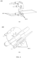
- FIG. 1 is a schematic diagram of a structure of a charging connector 100 according to this application.
- the charging connector 100 includes a connector body 101, a connector head 102 disposed at a front end of the connector body 101, and a handle 103 disposed at the other end of the connector body 101.
- the handle 103 is connected to the connector body 101 at a specific angle in an inclined manner.
- a lock hook 104 for locking the charging connector 100 is disposed on one side of the connector body 101, and a lock hook button 105 is disposed on the other side that is of the connector body 101 and that is close to the handle 103.
- the lock hook button 105 is configured to control locking or unlocking of the charging connector 100.
- a cable 106 is connected to a rear end of the connector body 101.
- the cable 106 is configured to connect a charging pile (not shown in the figure) and the charging connector 100, so that the charging pile charges the charging connector 100.
- a terminal connection structure 200 provided in this application is used in a terminal mounting position 110 in FIG. 1 (for example, an area in a dashed box in FIG. 1 ).
- each charging connector terminal corresponds to one cable, and a terminal is connected to a signal cable in a crimping or welding manner.
- each terminal is fastened to a housing of the charging connector by using a fastening clamping seat.
- Embodiments of this application provide a charging connector and a terminal connection structure of the charging connector, so that fastening and assembling of terminals of the existing charging connector can be simplified, and more space is reserved for heat exchange of a connector head of the charging connector.
- FIG. 2 is a schematic diagram of a terminal connection structure 200 in a charging connector according to an embodiment of this application.
- FIG. 2 shows the terminal connection structure 200.
- the terminal connection structure 200 is disposed in the connector head 102.
- the terminal connection structure 200 may include a first PCB 201 and a second PCB 203.
- the first PCB 201 is fixedly connected to a housing (not shown in the figure) of the connector head 102 through screw holes 204, and is connected to the second PCB 203 through an inter-PCB connection port 202.
- the first PCB 201 mainly transmits a signal of each terminal to the second PCB 203 through the inter-PCB connection port 202, and serves as a fastening support to provide limiting and fastening functions for each terminal.
- An integrated processor is disposed on the second PCB 203.
- the second PCB 203 mainly processes signals from a signal terminal and a sensor, and implements communication with a charging pile (not shown in the figure) based on the signals from the signal terminal and the sensor.
- first PCB 201 and the second PCB 203 may be connected through a pin terminal, or may be connected through a flexible cable. It should be understood that this is not limited in this embodiment of this application.
- first PCB 201 when the first PCB 201 is connected to the second PCB 203 through the pin terminal, the first PCB 201 and the second PCB 203 are vertically connected. As shown in FIG. 2 , the first PCB 201 and the second PCB 203 are connected at a vertical angle. However, when the first PCB 201 is connected to the second PCB 203 through the flexible cable, the first PCB 201 and the second PCB 203 are fixedly connected at any angle. It should be understood that this is not limited in this embodiment of this application.
- FIG. 3 is a schematic diagram of a terminal connection structure according to another embodiment of this application.
- the charging connector 100 includes the first PCB 201, a signal terminal 301, and the second PCB 203.
- the first PCB 201 is fixedly connected to the housing of the connector head 102 through the screw holes 204, and the first PCB 201 is provided with at least one first through hole 3011.
- one end of the signal terminal is fixedly connected to the first PCB 201 through the at least one first through hole 3011, and the other end of the signal terminal 301 is configured to connect to an electric vehicle.
- the other end of the signal terminal 301 may be connected to a socket (not shown in the figure) on the electric vehicle, and the signal terminal is configured to transmit a signal of the electric vehicle to the first PCB 201.
- the first PCB 201 transmits the signal from the signal terminal 301 to the second PCB 203 through an inter-PCB connection port 202, and the second PCB 203 processes the signal from the signal terminal 301 by using an integrated processor, and communicates with a charging pile (not shown in the figure) based on the signal.
- the signal from the signal terminal 301 may be used to determine whether the charging connector is connected to a charging port on the electric vehicle in place, or the signal from the signal terminal 301 may be communication information between the charging pile and the signal terminal 301.
- the charging pile sends identification information to a vehicle system of the electric vehicle by using the signal terminal 301, and then the vehicle system of the electric vehicle sends vehicle information to the charging pile by using the signal terminal 301.
- the signal terminal 301 may be connected to the first PCB 201 in a welding manner through the first through hole 3011.
- the welding manner includes but is not limited to submerged arc welding, arc welding, argon arc welding, and the like. It should be understood that this is not limited in this embodiment of this application.
- the signal terminal 301 may alternatively be connected to the first PCB 201 in a jack interference fit manner through the first through hole 3011.
- the jack may be a copper jack, or may be made of another conductive metal material. It should be understood that this is not limited in this embodiment of this application.
- FIG. 4 is a schematic diagram of a terminal connection structure 200 according to another embodiment of this application.
- the charging connector 100 further includes an auxiliary power supply terminal 401, and the first PCB 201 is further provided with at least one second through hole 4011.
- the first PCB 201 is fixedly connected to the housing of the connector head 102 through the screw holes 204, and is connected to the second PCB 203 through the inter-PCB connection port 202.
- one end of the auxiliary power supply terminal 401 is fixedly connected to the first PCB 201 through the at least one second through hole 4011, and the other end of the auxiliary power supply terminal 401 is configured to connect to the electric vehicle.
- the other end of the auxiliary power supply terminal 401 is connected to a charging port on the electric vehicle, and the auxiliary power supply terminal is configured to transmit a current signal provided by an auxiliary power supply in the charging pile to the electric vehicle.
- auxiliary power supply terminal 401 One end of the auxiliary power supply terminal 401 is fixedly connected to the first PCB 201, the first PCB 201 is connected to the second PCB 203 through the inter-PCB connection port 202.
- One end of the second PCB 203 is crimped with a cable (not shown in the figure), and is connected to the charging pile through the cable.
- the current signal of the auxiliary power supply in the charging pile is transmitted to the second PCB 203 through the cable, and then the current signal is transmitted to the first PCB 201 and the auxiliary power supply terminal 401.
- the auxiliary power supply terminal 401 wakes up a vehicle control unit (vehicle control unit, VCU) through the charging port.
- VCU vehicle control unit
- the auxiliary power supply in the charging pile provides the current signal to the auxiliary power supply terminal 401, and then the auxiliary power supply terminal 401 provides the current signal provided by the auxiliary power supply in the charging pile to the charging port of the electric vehicle, to charge a battery management system (battery management system, BMS) and the VCU in the vehicle.
- BMS battery management system
- one end of the auxiliary power supply terminal 401 may be connected to the first PCB 201 in a welding manner through the at least one second through hole 4011.
- the welding manner includes but is not limited to submerged arc welding, arc welding, argon arc welding, and the like. It should be understood that this is not limited in this embodiment of this application.
- one end of the auxiliary power supply terminal 401 is fixedly connected to the first PCB 201 through the second through hole 4011, or may be fixedly connected to the first PCB 201 in a jack interference fit manner.
- the jack may be a copper jack, or may be made of another conductive metal material. It should be understood that this is not limited in this embodiment of this application.
- the auxiliary power supply terminal 401 may alternatively be fixedly connected to the first PCB 201 in a fitting manner through the second through hole 4011, the other end of the auxiliary power supply terminal 401 is connected to the charging port on the electric vehicle.
- the auxiliary power supply terminal 401 is configured to transmit the current signal provided by the auxiliary power supply in the charging pile to the electric vehicle.
- a cable is further crimped at one end that is of the auxiliary power supply terminal and that is connected to the first PCB.
- the cable is configured to connect to the charging pile.
- the auxiliary power supply in the charging pile provides the current signal to the auxiliary power supply terminal 401 through the cable.
- the second through hole 4011 may be an unclosed hole. As shown in (b) in FIG. 4 , the second through hole 4011 may be an unclosed hole at a bottom. Such a design facilitates mounting of the auxiliary power supply terminal 401 from the bottom.
- the second through hole 4011 may alternatively be a hole with an internal thread structure.
- one end that is of the auxiliary power supply terminal 401 and that is close to the first PCB 201 is provided with an external thread structure matching the internal thread structure, so that the auxiliary power supply terminal 401 is tightly fit with the first PCB 201 through the second through hole 4011.
- FIG. 5 is a schematic diagram of a terminal connection structure 200 according to another embodiment of this application.
- the charging connector 100 further includes a power terminal 501.
- One end of the power terminal 501 is fixedly connected to the first PCB 201 in a fitting manner through at least one third through hole 5011, and the other end of the power terminal 501 is connected to the electric vehicle.
- the power terminal 501 is configured to transmit a charging current signal to the electric vehicle.
- the power terminal 501 is configured to provide a high-power charging current to a charging port on the electric vehicle, to fast charge the electric vehicle.
- the third through hole 5011 may be an unclosed hole. As shown in FIG. 5 , the third through hole 5011 may be an unclosed hole on a side surface. Such a design facilitates mounting of the power terminal 501 from the side surface.
- the third through hole 5011 may alternatively be a hole with an internal thread structure.
- one end that is of the power terminal 501 and that is close to the first PCB 201 is provided with an external thread structure matching the internal thread structure, so that the power terminal 501 is tightly fit with the first PCB 201 through the third through hole 5011.
- FIG. 6 is a schematic diagram of a terminal connection structure 200 according to another embodiment of this application.
- the charging connector 100 further includes a ground wire terminal 601.
- the ground wire terminal 601 is fixedly connected to the first PCB 201 in a fitting manner through a fourth through hole 6011, and the other end of the ground wire terminal 601 is connected to the electric vehicle.
- the ground wire terminal 601 is mainly used for protection, to avoid a non-safety accident when the charging pile charges the electric vehicle by using the charging connector.
- the fourth through hole 6011 may alternatively be a hole with an internal thread structure.
- one end that is of the ground wire terminal 601 and that is close to the first PCB 201 is provided with an external thread structure matching the internal thread structure, so that the ground wire terminal 601 is tightly fit with the first PCB 201 through the fourth through hole 6011.
- the fourth through hole 6011 may be an unclosed hole. As shown in (b) in FIG. 4 , the fourth through hole 6011 may be an unclosed hole at a bottom. Such a design facilitates mounting of the ground wire terminal 601 from the bottom.
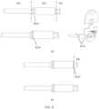
- FIG. 7 is a schematic diagram of a structure of a signal terminal according to an embodiment of this application.
- the signal terminal 301 is sequentially arranged with a body portion 710, a fastening portion 720, and a through hole connection portion 730 in an axial direction thereof.
- the body portion 710 of the signal terminal 301 is tightly connected to the housing of the connector head 102, and the fastening portion 720 of the signal terminal 301 is provided with a boss 7210.
- the through hole connection portion 730 of the signal terminal 301 is fixedly connected to the first PCB 201 in a welding or jack manner through the first through hole 3011.
- a diameter of the boss 7210 is usually set to be greater than a diameter of the first through hole 3011.
- a sealing ring mounting groove 7220 is mounted at one end that is of the fastening portion 720 of the signal terminal 301 and that is close to the body portion 710.
- the sealing ring mounting groove 7220 is configured to mount a sealing ring 7230, so that the signal terminal 301 is tightly connected to the first through hole 3011, to prevent the signal terminal 301 from rotating in an axial direction.
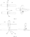
- FIG. 8 is a schematic diagram of a structure of an auxiliary power supply terminal according to an embodiment of this application.
- the auxiliary power supply terminal 401 is connected to the first PCB 201 in a welding or jack manner.
- a specific connection manner is described above.
- the auxiliary power supply terminal 401 is sequentially arranged with a body portion 810, a fastening portion 820, and a through hole connection portion 830 in an axial direction thereof.
- the body portion 810 of the auxiliary power supply terminal 401 is tightly connected to the housing of the connector head 102.
- the fastening portion 820 of the auxiliary power supply terminal 401 is provided with a boss 8210.
- the through hole connection portion 830 of the auxiliary power supply terminal and the second through hole 4011 are fixedly connected to the first PCB 201 in a welding or jack manner.
- a diameter of the boss 8210 is usually set to be greater than a diameter of the second through hole 4011.
- a sealing ring mounting groove 8220 is mounted at one end that is of the fastening portion 820 of the auxiliary power supply terminal 401 and that is close to the body portion 810.
- the sealing ring mounting groove 8220 is configured to mount a sealing ring 8230, so that the auxiliary power supply terminal 401 is tightly connected to the second through hole 4011, to prevent the auxiliary power supply terminal 401 from rotating in an axial direction.
- the auxiliary power supply terminal 401 may alternatively be connected to the first PCB 201 in a fitting manner through the second through hole 4011. It should be understood that, for a specific fitting manner, refer to the foregoing description. Details are not described herein again in this application.
- the auxiliary power supply terminal 401 is sequentially arranged with a body portion 810, a fastening portion 820, and a cable connection portion 840 in an axial direction thereof.
- the body portion 810 of the auxiliary power supply terminal 401 is tightly connected to the housing of the connector head 102.
- the fastening portion 820 of the auxiliary power supply terminal 401 is provided with a boss 8210.
- the cable connection portion 840 of the auxiliary power supply terminal is fixedly connected to the first PCB 201 in a fitting manner through the second through hole 4011, and is connected to the cable connected to the charging pile.
- a PCB mounting groove 8250 is mounted at one end that is of the fastening portion 820 of the auxiliary power supply terminal 401 and that is close to the cable connection portion 440.
- the PCB mounting groove 8250 may be of a circular or non-circular structure.
- the PCB mounting groove 8250 may be of a cylindrical structure shown in (b) in FIG. 8 , or may be of a square structure shown in (b) in FIG. 8 .
- a function of the PCB mounting groove is to prevent the auxiliary power supply terminal 401 from rotating in an axial direction in a process of using the charging connector.
- FIG. 9 is a schematic diagram of a structure of a power terminal according to an embodiment of this application.
- the power terminal 501 is sequentially arranged with a body portion 910, a fastening portion 920, and a cable connection portion 930 in an axial direction thereof.
- the body portion 910 of the power terminal 501 is tightly connected to the housing of the connector head 102.
- the fastening portion 920 of the power terminal 501 is provided with a boss 9210.
- the cable connection portion 930 of the power terminal 501 is connected to the first PCB 201 in a fitting manner through the third through hole 5011, and is connected to the cable connected to the charging pile.
- a diameter of the boss 9210 is usually set to be greater than the third through hole 5011.
- a sealing ring mounting groove 9220 is mounted at one end that is of the fastening portion 920 of the power terminal 501 and that is close to the body portion 910.
- the sealing ring mounting groove 9220 is configured to mount a sealing ring 9230, so that the power terminal 501 is tightly connected to the first PCB 201 through the third through hole 5011, to prevent the power terminal 501 from rotating in an axial direction.
- a PCB mounting groove 9240 is mounted at one end that is of the fastening portion 920 of the power terminal 501 and that is close to the cable connection portion 930.
- the PCB mounting groove 9240 may be of a non-circular structure, to prevent the power terminal 501 from rotating in an axial direction in a process of using the charging connector.
- FIG. 10 is a schematic diagram of a structure of a ground wire terminal according to an embodiment of this application.
- the ground wire terminal 601 is sequentially arranged with a body portion 1010, a fastening portion 1020, and a cable connection portion 1030 in an axial direction thereof.
- the body portion 1010 of the ground wire terminal 601 is tightly connected to the housing of the connector head 102.
- the fastening portion 1020 of the ground wire terminal 601 is provided with a boss 1021.
- the cable connection portion 1030 of the ground wire terminal 601 is connected to the first PCB 201 in a fitting manner through the fourth through hole 6011, and is connected to the cable of the charging pile.
- a diameter of the boss 1021 is usually set to be greater than the fourth through hole 6011.
- a sealing ring mounting groove 1022 is mounted at one end that is of the fastening portion 1020 of the ground wire terminal 601 and that is close to the body portion 1010 of the ground wire terminal 601.
- the sealing ring mounting groove 1022 is configured to mount a sealing ring 1023, so that the ground wire terminal 601 is tightly connected to the first PCB 201 through the fourth through hole 6011, to prevent the ground wire terminal 601 from rotating in an axial direction.
- a PCB mounting groove 1024 is mounted at one end that is of the fastening portion 1020 of the ground wire terminal 601 and that is close to the cable connection portion 1030.
- the PCB mounting groove 1024 may be of a non-circular structure, to prevent the ground wire terminal 601 from rotating in an axial direction in a process of using the charging connector.
- PCB mounting groove described above may be of a rectangular structure, a triangular structure, or a diamond structure. It should be understood that this is not limited in this embodiment of this application.
- FIG. 11 is a schematic diagram of a structure of a charging pile according to an embodiment of this application.
- a charging pile 300 includes a charging pile body 310 and a charging connector 100.
- the charging connector 100 is connected to the charging pile body 310.
- one end of the charging connector 100 is connected to the charging pile 310 through a connection cable (not shown in the figure).
Landscapes
- Engineering & Computer Science (AREA)
- Microelectronics & Electronic Packaging (AREA)
- Manufacturing & Machinery (AREA)
- Power Engineering (AREA)
- Transportation (AREA)
- Mechanical Engineering (AREA)
- Electric Propulsion And Braking For Vehicles (AREA)
- Charge And Discharge Circuits For Batteries Or The Like (AREA)
Abstract
Description
- This application relates to the field of new energy vehicle charging, and specifically, to a charging connector and a charging pile.
- With development of society and progress of science and technology, new energy vehicles have been favored by an increasing number of consumers, and importance of charging supporting devices related to the new energy vehicles has gradually become prominent. A charging connector is an indispensable device for charging an electric vehicle, and the charging connector is a connection apparatus for transferring electrical energy from a charging pile device to an energy storage battery of the electric vehicle. For a direct-current charging connector, a charging interface of the direct-current charging connector usually includes components such as a signal terminal, an auxiliary power supply terminal, a power terminal, and a ground wire terminal. However, the plurality of terminal components result in a complex connection structure of the charging connector, and affect production and assembling efficiency.
- In addition, "charging anxiety" is also one of key problems that restrict the development of the new energy vehicles. Usually, a charging current is increased to improve charging power. However, as the charging current continuously increases, heat generated by the plurality of terminals in the charging connector also continuously increases. Therefore, a heat exchange component usually needs to be added to dissipate heat for components such as a terminal and a cable assembly in the charging connector. Consequently, a higher requirement is also imposed on internal space of a connector head of the charging connector.
- In conclusion, how to perform integrated design to reduce complexity of an internal structure of the charging connector is a key path to improve production and assembling efficiency and reduce costs.
- This application provides a charging connector and a charging pile, so that fastening and assembling of terminals of an existing charging connector can be simplified, and more space is reserved for heat exchange of a connector head of the charging connector.
- According to a first aspect, a charging connector for charging an electric vehicle is provided, and includes a connector body, a connector head, and a terminal connection structure. The connector head is disposed at a front end of the connector body, and the terminal connection structure is disposed in the connector head. The terminal connection structure includes: a first PCB, where the first PCB is fixedly connected to a housing of the connector head, and the first PCB is provided with at least one first through hole; a signal terminal, configured to transmit a signal sent by the electric vehicle, where one end of the signal terminal is fixedly connected to the first PCB through the at least one first through hole, and the other end of the signal terminal is configured to connect to the electric vehicle; and a second PCB connected to the first PCB, where the second PCB is configured to process the signal from the signal terminal. According to the technical solution of this application, one end of the signal terminal is fixedly connected to the first PCB through the at least one first through hole, and the other end of the signal terminal is connected to the electric vehicle. The signal from the signal terminal is transmitted to the second PCB through the first PCB, and the second PCB processes the signal from the signal terminal, to implement communication with a charging pile based on the signal. In the foregoing technical solution, a cable connection manner is avoided, so that fastening and assembling of terminals of the charging connector can be simplified, and more space is reserved for heat exchange of the connector head of the charging connector.
- With reference to the first aspect, in some implementations of the first aspect, the signal terminal is connected to the first PCB in any one of welding and jack manners through the at least one first through hole.
- According to the technical solution of this application, the signal terminal is connected to the first PCB through the at least one first through hole, to avoid using the cable connection manner, so that fastening and assembling of terminals of the charging connector can be simplified, and more space is reserved for heat exchange of the connector head of the charging connector.
- With reference to the first aspect, in some implementations of the first aspect, an auxiliary power supply terminal is further included, and is configured to transmit a current signal provided by an auxiliary power supply to the electric vehicle. One end of the auxiliary power supply terminal is connected to the first PCB through at least one second through hole, and the other end of the auxiliary power supply terminal is configured to connect to the electric vehicle. According to the technical solution of this application, one end of the auxiliary power supply terminal is connected to the first PCB through the at least one second through hole, to avoid the cable connection manner, so that fastening and assembling of terminals of the charging connector can be simplified, and more space is reserved for heat exchange of the connector head of the charging connector.
- With reference to the first aspect, in some implementations of the first aspect, the auxiliary power supply terminal is connected to the first PCB in any one of welding and jack manners through the at least one second through hole.
- According to the technical solution of this application, the auxiliary power supply terminal is connected to the first PCB in the welding or jack manner through the at least one second through hole, so that fastening and assembling of terminals of the charging connector can be simplified, and more space is reserved for heat exchange of the connector head of the charging connector.
- With reference to the first aspect, in some implementations of the first aspect, an auxiliary power supply terminal is further included, and is configured to transmit a current signal provided by an auxiliary power supply to the electric vehicle. One end of the auxiliary power supply terminal is fastened to the first PCB through at least one second through hole, and the other end of the auxiliary power supply terminal is configured to connect to the electric vehicle.
- In a possible implementation, the second through hole may be set as an unclosed hole, so that the auxiliary power supply terminal is mounted from a bottom of the first PCB.
- According to the technical solution of this application, the auxiliary power supply terminal is fixedly connected to the first PCB through the at least one second through hole, so that fastening and assembling of terminals of the charging connector can be simplified.
- With reference to the first aspect, in some implementations of the first aspect, a power terminal is further included, and is configured to transmit a charging current signal to the electric vehicle. One end of the power terminal is fastened to the first PCB in a fitting manner through at least one third through hole, and the other end of the power terminal is configured to connect to the electric vehicle.
- In a possible implementation, the third through hole may be set as an unclosed hole, so that the power terminal is mounted from a side surface of the first PCB.
- According to the technical solution of this application, the power terminal is fixedly connected to the first PCB in the fitting manner through at least one through hole, so that fastening and assembling of terminals of the charging connector can be simplified.
- With reference to the first aspect, in some implementations of the first aspect, a ground wire terminal is further included. The ground wire terminal is fastened to the first PCB through at least one fourth through hole.
- In a possible implementation, the fourth through hole may be set as an unclosed hole, so that the ground wire terminal is mounted from the bottom of the first PCB.
- According to the technical solution of this application, the ground wire terminal is fixedly connected to the first PCB in the fitting manner through at least one through hole, so that fastening and assembling of terminals of the charging connector can be simplified.
- With reference to the first aspect, in some implementations of the first aspect, the signal terminal includes a body portion, a fastening portion, and a through hole connection portion that are sequentially arranged in an axial direction of the signal terminal. The through hole connection portion is connected to the first through hole, the fastening portion is provided with a boss, and a diameter of the boss is greater than a diameter of the first through hole. According to the foregoing technical solution, fastening and assembling of terminals of the charging connector can be simplified, and more space is reserved for heat exchange of the connector head of the charging connector.
- With reference to the first aspect, in some implementations of the first aspect, the auxiliary power supply terminal includes a body portion, a fastening portion, and a through hole connection portion that are sequentially arranged in an axial direction of the auxiliary power supply terminal. The through hole connection portion is connected to the second through hole, the fastening portion is provided with a boss, and a diameter of the boss is greater than a diameter of the second through hole. According to the foregoing technical solution, fastening and assembling of terminals of the charging connector can be simplified, and more space is reserved for heat exchange of the connector head of the charging connector.
- With reference to the first aspect, in some implementations of the first aspect, the auxiliary power supply terminal includes a body portion, a fastening portion, and a cable connection portion that are sequentially arranged in an axial direction of the auxiliary power supply terminal. The cable connection portion is connected to the second through hole, the fastening portion is provided with a boss, and a diameter of the boss is greater than the second through hole. According to the foregoing technical solution, fastening and assembling of terminals of the charging connector can be simplified, and more space is reserved for heat exchange of the connector head of the charging connector.
- With reference to the first aspect, in some implementations of the first aspect, the power terminal includes a body portion, a fastening portion, and a cable connection portion that are sequentially arranged in an axial direction of the power terminal. The cable connection portion is connected to the third through hole, the fastening portion is provided with a boss, and a diameter of the boss is greater than the third through hole. According to the foregoing technical solution, fastening and assembling of terminals of the charging connector can be simplified, and more space is reserved for heat exchange of the connector head of the charging connector.
- With reference to the first aspect, in some implementations of the first aspect, the ground wire terminal includes a body portion, a fastening portion, and a cable connection portion that are sequentially arranged in an axial direction of the ground wire terminal. The cable connection portion is connected to the fourth through hole, the fastening portion is provided with a boss, and a diameter of the boss is greater than the fourth through hole. According to the foregoing technical solution, fastening and assembling of terminals of the charging connector can be simplified, and more space is reserved for heat exchange of the connector head of the charging connector.
- With reference to the first aspect, in some implementations of the first aspect, a sealing ring mounting groove is mounted at one end that is of the fastening portion and that is close to the body portion. According to the foregoing technical solution, fastening and assembling of terminals of the charging connector can be simplified, and more space is reserved for heat exchange of the connector head of the charging connector.
- With reference to the first aspect, in some implementations of the first aspect, a sealing ring mounting groove is mounted at one end that is of the fastening portion and that is close to the body portion. According to the foregoing technical solution, fastening and assembling of terminals of the charging connector can be simplified, and more space is reserved for heat exchange of the connector head of the charging connector.
- With reference to the first aspect, in some implementations of the first aspect, a sealing ring mounting groove is mounted at one end that is of the fastening portion and that is close to the body portion. According to the foregoing technical solution, fastening and assembling of terminals of the charging connector can be simplified, and more space is reserved for heat exchange of the connector head of the charging connector.
- With reference to the first aspect, in some implementations of the first aspect, a sealing ring mounting groove is mounted at one end that is of the fastening portion and that is close to the body portion. According to the foregoing technical solution, fastening and assembling of terminals of the charging connector can be simplified, and more space is reserved for heat exchange of the connector head of the charging connector.
- With reference to the first aspect, in some implementations of the first aspect, a PCB mounting groove is mounted at one end that is of the fastening portion and that is close to the cable connection portion. According to the foregoing technical solutions, the terminal can be prevented from rotating in the axial direction, fastening and assembling of terminals of the charging connector are simplified, and more space is reserved for heat exchange of the connector head of the charging connector.
- According to a second aspect, a charging pile is provided, and includes a charging pile body and a charging connector. The charging connector is connected to the charging pile body. The charging connector includes a connector body, a connector head, and a terminal connection structure. The connector head is disposed at a front end of the connector body, and the terminal connection structure is disposed in the connector head. The terminal connection structure includes: a first PCB, where the first PCB is fixedly connected to a housing of the connector head, and the first PCB is provided with at least one first through hole; a signal terminal, configured to transmit a signal sent by an electric vehicle, where one end of the signal terminal is fixedly connected to the first PCB through the at least one first through hole, and the other end of the signal terminal is configured to connect to the electric vehicle; and a second PCB connected to the first PCB, where the second PCB is configured to process the signal from the signal terminal. According to the technical solution of this application, one end of the signal terminal is fixedly connected to the first PCB through the at least one first through hole, and the other end of the signal terminal is connected to the electric vehicle. The signal from the signal terminal is transmitted to the second PCB through the first PCB, and the second PCB processes the signal from the signal terminal. In the foregoing technical solution, a cable connection manner is avoided, so that fastening and assembling of terminals of the charging connector can be simplified, and more space is reserved for heat exchange of the connector head of the charging connector.
- With reference to the second aspect, in some implementations of the second aspect, the signal terminal is connected to the first PCB in any one of welding and jack manners through the at least one first through hole.
- With reference to the second aspect, in some implementations of the second aspect, the charging pile body further includes an auxiliary power supply, and the charging connector further includes an auxiliary power supply terminal. The auxiliary power supply terminal is configured to transmit a current signal provided by the auxiliary power supply to the electric vehicle. One end of the auxiliary power supply terminal is connected to the first PCB through at least one second through hole, and transmits the signal of the auxiliary power supply terminal to the first PCB, and the other end of the auxiliary power supply terminal is configured to connect to the electric vehicle.
- With reference to the second aspect, in some implementations of the second aspect, the auxiliary power supply terminal is connected to the first PCB in any one of welding and jack manners through the at least one second through hole.
- With reference to the second aspect, in some implementations of the second aspect, the charging pile body further includes an auxiliary power supply, and the charging connector further includes an auxiliary power supply terminal. The auxiliary power supply terminal is configured to transmit a current signal provided by the auxiliary power supply to the electric vehicle. One end of the auxiliary power supply terminal is fastened to the first PCB through at least one second through hole, and the other end of the auxiliary power supply terminal is configured to connect to the electric vehicle.
- With reference to the second aspect, in some implementations of the second aspect, the charging pile body further includes a power module, and the charging connector further includes a power terminal. The power terminal is configured to transmit a charging current signal provided by the power module to the electric vehicle. One end of the power terminal is fastened to the first PCB through at least one third through hole, and the other end of the power terminal is configured to connect to the electric vehicle.
- With reference to the second aspect, in some implementations of the second aspect, a ground wire terminal is further included. The ground wire terminal is fastened to the first PCB through at least one fourth through hole.
- With reference to the second aspect, in some implementations of the second aspect, the signal terminal includes a body portion, a fastening portion, and a through hole connection portion that are sequentially arranged in an axial direction of the signal terminal. The through hole connection portion is connected to the first through hole, the fastening portion is provided with a boss, and a diameter of the boss is greater than a diameter of the first through hole.
- With reference to the second aspect, in some implementations of the second aspect, the auxiliary power supply terminal includes a body portion, a fastening portion, and a through hole connection portion that are sequentially arranged in an axial direction of the auxiliary power supply terminal. The through hole connection portion is connected to the second through hole, the fastening portion is provided with a boss, and a diameter of the boss is greater than a diameter of the second through hole.
- With reference to the second aspect, in some implementations of the second aspect, the auxiliary power supply terminal includes a body portion, a fastening portion, and a cable connection portion that are sequentially arranged in an axial direction of the auxiliary power supply terminal. The cable connection portion is connected to the second through hole, the fastening portion is provided with a boss, and a diameter of the boss is greater than the second through hole.
- With reference to the second aspect, in some implementations of the second aspect, the power terminal includes a body portion, a fastening portion, and a cable connection portion that are sequentially arranged in an axial direction of the power terminal. The cable connection portion is connected to the third through hole, the fastening portion is provided with a boss, and a diameter of the boss is greater than the third through hole.
- With reference to the second aspect, in some implementations of the second aspect, the ground wire terminal includes a body portion, a fastening portion, and a cable connection portion that are sequentially arranged in an axial direction of the ground wire terminal. The cable connection portion is connected to the fourth through hole, the fastening portion is provided with a boss, and a diameter of the boss is greater than the fourth through hole.
- With reference to the second aspect, in some implementations of the second aspect, a sealing ring mounting groove is mounted at one end that is of the fastening portion and that is close to the body portion.
- With reference to the second aspect, in some implementations of the second aspect, a sealing ring mounting groove is mounted at one end that is of the fastening portion and that is close to the body portion.
- With reference to the second aspect, in some implementations of the second aspect, a sealing ring mounting groove is mounted at one end that is of the fastening portion and that is close to the body portion.
- With reference to the second aspect, in some implementations of the second aspect, a sealing ring mounting groove is mounted at one end that is of the fastening portion and that is close to the body portion.
- With reference to the second aspect, in some implementations of the second aspect, a PCB mounting groove is mounted at one end that is of the fastening portion and that is close to the cable connection portion.
-
-
FIG. 1 is a schematic diagram of a structure of a charging connector according to an embodiment of this application; -
FIG. 2 is a schematic diagram of a terminal connection structure of a charging connector according to an embodiment of this application; -
FIG. 3 is a schematic diagram of a terminal connection structure of a charging connector according to another embodiment of this application; -
FIG. 4 is a schematic diagram of a terminal connection structure of a charging connector according to another embodiment of this application; -
FIG. 5 is a schematic diagram of a terminal connection structure of a charging connector according to another embodiment of this application; -
FIG. 6 is a schematic diagram of a terminal connection structure of a charging connector according to another embodiment of this application; -
FIG. 7 is a schematic diagram of a structure of a signal terminal according to an embodiment of this application; -
FIG. 8 is a schematic diagram of a structure of an auxiliary power supply terminal according to an embodiment of this application; -
FIG. 9 is a schematic diagram of a structure of a power terminal according to an embodiment of this application; -
FIG. 10 is a schematic diagram of a structure of a ground wire terminal according to an embodiment of this application; and -
FIG. 11 is a schematic diagram of a structure of a charging pile according to an embodiment of this application. - 100: charging connector; 101: connector body of the charging connector; 102: connector head of the charging connector; 103: handle; 104: lock hook; 105: lock hook button; 106: cable; 110: terminal mounting position; 201: first PCB; 202: inter-PCB connection port; 203: second PCB; 204: screw hole; 301: signal terminal; 3011: first through hole; 401: auxiliary power supply terminal; 4011: second through hole; 501: power terminal; 5011: third through hole; 601: ground wire terminal; 6011: fourth through hole; 710: body portion; 720: fastening portion; 730: through hole connection portion; 7210: boss; 7220: sealing ring mounting groove; 7230: sealing ring; 810: body portion; 820: fastening portion; 830: through hole connection portion; 8210: boss; 8220: sealing ring mounting groove; 8230: sealing ring; 840: cable connection portion; 8250: PCB mounting groove; 910: body portion; 920: fastening portion; 930: cable connection portion; 9210: boss; 9220: sealing ring mounting groove; 9230: sealing ring; 1010: body portion; 1020: fastening portion; 1030: cable connection portion; 1021: boss; 1022: sealing ring mounting groove; 1023: sealing ring; 1024: PCB mounting groove.
- The following describes technical solutions of embodiments in this application with reference to the accompanying drawings.
- The following describes embodiments of this application in detail. Examples of embodiments of this application are shown in the accompanying drawings. In the accompanying drawings, same or similar reference numerals represent same or similar elements or elements having same or similar functions. The embodiments described below with reference to the accompanying drawings are examples, and are merely used to explain this application, but shall not be understood as a limitation on this application.
- In descriptions of this application, it should be noted that, unless otherwise clearly specified and limited, the terms "mounting", "connection to", and "connection" should be understood in a broad sense. For example, the connection may be a fixed connection, may be an indirect connection by using an intermediate medium, or may be an internal connection between two elements or an interaction relationship between two elements. A person of ordinary skill in the art may interpret specific meanings of the foregoing terms in this application according to specific cases.
- It should be noted that a terminal connection structure of a charging connector provided in embodiments of this application may be used in a charging connector. The charging connector may be a naturally cooled charging connector, a liquid-cooled charging connector, a charging pile, or the like. This is not limited in this application.
-
FIG. 1 is a schematic diagram of a structure of a chargingconnector 100 according to this application. - As shown in
FIG. 1 , the chargingconnector 100 includes aconnector body 101, aconnector head 102 disposed at a front end of theconnector body 101, and ahandle 103 disposed at the other end of theconnector body 101. Thehandle 103 is connected to theconnector body 101 at a specific angle in an inclined manner. Alock hook 104 for locking the chargingconnector 100 is disposed on one side of theconnector body 101, and alock hook button 105 is disposed on the other side that is of theconnector body 101 and that is close to thehandle 103. Thelock hook button 105 is configured to control locking or unlocking of the chargingconnector 100. Acable 106 is connected to a rear end of theconnector body 101. Thecable 106 is configured to connect a charging pile (not shown in the figure) and the chargingconnector 100, so that the charging pile charges the chargingconnector 100. It should be noted that aterminal connection structure 200 provided in this application is used in aterminal mounting position 110 inFIG. 1 (for example, an area in a dashed box inFIG. 1 ). - Currently, a method for connecting a charging connector terminal to a cable is usually used. Specifically, each charging connector terminal corresponds to one cable, and a terminal is connected to a signal cable in a crimping or welding manner. In addition, each terminal is fastened to a housing of the charging connector by using a fastening clamping seat.
- Each terminal needs to be connected to a cable. As a result, problems such as a complex cable connection and low assembling automation occur on each terminal of the entire charging connector. In addition, the fastening clamping seat is used to fasten each terminal to the housing of the charging connector. Due to a fact that space occupied by the fastening clamping seat is large, mounting of another heat dissipation component is not facilitated, and heat dissipation cannot be better performed on each terminal of the charging connector as well as a component such as a cable assembly. In conclusion, how to simplify fastening and assembling of terminals of the charging connector and reserve more space for heat exchange of the connector head of the charging connector becomes an urgent problem to be resolved. Embodiments of this application provide a charging connector and a terminal connection structure of the charging connector, so that fastening and assembling of terminals of the existing charging connector can be simplified, and more space is reserved for heat exchange of a connector head of the charging connector.
-
FIG. 2 is a schematic diagram of aterminal connection structure 200 in a charging connector according to an embodiment of this application. -
FIG. 2 shows theterminal connection structure 200. Theterminal connection structure 200 is disposed in theconnector head 102. Theterminal connection structure 200 may include afirst PCB 201 and asecond PCB 203. Thefirst PCB 201 is fixedly connected to a housing (not shown in the figure) of theconnector head 102 through screw holes 204, and is connected to thesecond PCB 203 through aninter-PCB connection port 202. - The
first PCB 201 mainly transmits a signal of each terminal to thesecond PCB 203 through theinter-PCB connection port 202, and serves as a fastening support to provide limiting and fastening functions for each terminal. An integrated processor is disposed on thesecond PCB 203. Thesecond PCB 203 mainly processes signals from a signal terminal and a sensor, and implements communication with a charging pile (not shown in the figure) based on the signals from the signal terminal and the sensor. - It should be noted that the
first PCB 201 and thesecond PCB 203 may be connected through a pin terminal, or may be connected through a flexible cable. It should be understood that this is not limited in this embodiment of this application. - It should be further noted that, when the
first PCB 201 is connected to thesecond PCB 203 through the pin terminal, thefirst PCB 201 and thesecond PCB 203 are vertically connected. As shown inFIG. 2 , thefirst PCB 201 and thesecond PCB 203 are connected at a vertical angle. However, when thefirst PCB 201 is connected to thesecond PCB 203 through the flexible cable, thefirst PCB 201 and thesecond PCB 203 are fixedly connected at any angle. It should be understood that this is not limited in this embodiment of this application. -
FIG. 3 is a schematic diagram of a terminal connection structure according to another embodiment of this application. As shown inFIG. 3 , the chargingconnector 100 includes thefirst PCB 201, asignal terminal 301, and thesecond PCB 203. Thefirst PCB 201 is fixedly connected to the housing of theconnector head 102 through the screw holes 204, and thefirst PCB 201 is provided with at least one first throughhole 3011. - Specifically, one end of the signal terminal is fixedly connected to the
first PCB 201 through the at least one first throughhole 3011, and the other end of thesignal terminal 301 is configured to connect to an electric vehicle. For example, the other end of thesignal terminal 301 may be connected to a socket (not shown in the figure) on the electric vehicle, and the signal terminal is configured to transmit a signal of the electric vehicle to thefirst PCB 201. In this case, thefirst PCB 201 transmits the signal from thesignal terminal 301 to thesecond PCB 203 through aninter-PCB connection port 202, and thesecond PCB 203 processes the signal from thesignal terminal 301 by using an integrated processor, and communicates with a charging pile (not shown in the figure) based on the signal. - The signal from the
signal terminal 301 may be used to determine whether the charging connector is connected to a charging port on the electric vehicle in place, or the signal from thesignal terminal 301 may be communication information between the charging pile and thesignal terminal 301. For example, the charging pile sends identification information to a vehicle system of the electric vehicle by using thesignal terminal 301, and then the vehicle system of the electric vehicle sends vehicle information to the charging pile by using thesignal terminal 301. - Optionally, in some embodiments, the
signal terminal 301 may be connected to thefirst PCB 201 in a welding manner through the first throughhole 3011. The welding manner includes but is not limited to submerged arc welding, arc welding, argon arc welding, and the like. It should be understood that this is not limited in this embodiment of this application. - Optionally, in some embodiments, the
signal terminal 301 may alternatively be connected to thefirst PCB 201 in a jack interference fit manner through the first throughhole 3011. The jack may be a copper jack, or may be made of another conductive metal material. It should be understood that this is not limited in this embodiment of this application. -
FIG. 4 is a schematic diagram of aterminal connection structure 200 according to another embodiment of this application. - Optionally, in some embodiments, as shown in (a) in
FIG. 4 , the chargingconnector 100 further includes an auxiliarypower supply terminal 401, and thefirst PCB 201 is further provided with at least one second throughhole 4011. Thefirst PCB 201 is fixedly connected to the housing of theconnector head 102 through the screw holes 204, and is connected to thesecond PCB 203 through theinter-PCB connection port 202. - Specifically, one end of the auxiliary
power supply terminal 401 is fixedly connected to thefirst PCB 201 through the at least one second throughhole 4011, and the other end of the auxiliarypower supply terminal 401 is configured to connect to the electric vehicle. In other words, the other end of the auxiliarypower supply terminal 401 is connected to a charging port on the electric vehicle, and the auxiliary power supply terminal is configured to transmit a current signal provided by an auxiliary power supply in the charging pile to the electric vehicle. - One end of the auxiliary
power supply terminal 401 is fixedly connected to thefirst PCB 201, thefirst PCB 201 is connected to thesecond PCB 203 through theinter-PCB connection port 202. One end of thesecond PCB 203 is crimped with a cable (not shown in the figure), and is connected to the charging pile through the cable. In this case, the current signal of the auxiliary power supply in the charging pile is transmitted to thesecond PCB 203 through the cable, and then the current signal is transmitted to thefirst PCB 201 and the auxiliarypower supply terminal 401. For example, the auxiliarypower supply terminal 401 wakes up a vehicle control unit (vehicle control unit, VCU) through the charging port. In addition, when the charging pile charges the electric vehicle by using the charging connector, the auxiliary power supply in the charging pile provides the current signal to the auxiliarypower supply terminal 401, and then the auxiliarypower supply terminal 401 provides the current signal provided by the auxiliary power supply in the charging pile to the charging port of the electric vehicle, to charge a battery management system (battery management system, BMS) and the VCU in the vehicle. - Optionally, in some embodiments, one end of the auxiliary
power supply terminal 401 may be connected to thefirst PCB 201 in a welding manner through the at least one second throughhole 4011. The welding manner includes but is not limited to submerged arc welding, arc welding, argon arc welding, and the like. It should be understood that this is not limited in this embodiment of this application. - Optionally, in some embodiments, one end of the auxiliary
power supply terminal 401 is fixedly connected to thefirst PCB 201 through the second throughhole 4011, or may be fixedly connected to thefirst PCB 201 in a jack interference fit manner. The jack may be a copper jack, or may be made of another conductive metal material. It should be understood that this is not limited in this embodiment of this application. - Optionally, in some embodiments, in the
terminal connection structure 200, the auxiliarypower supply terminal 401 may alternatively be fixedly connected to thefirst PCB 201 in a fitting manner through the second throughhole 4011, the other end of the auxiliarypower supply terminal 401 is connected to the charging port on the electric vehicle. The auxiliarypower supply terminal 401 is configured to transmit the current signal provided by the auxiliary power supply in the charging pile to the electric vehicle. - When the auxiliary
power supply terminal 401 is fixedly connected to thefirst PCB 201 in the fitting manner, a cable is further crimped at one end that is of the auxiliary power supply terminal and that is connected to the first PCB. The cable is configured to connect to the charging pile. In this case, the auxiliary power supply in the charging pile provides the current signal to the auxiliarypower supply terminal 401 through the cable. - It should be understood that the second through
hole 4011 may be an unclosed hole. As shown in (b) inFIG. 4 , the second throughhole 4011 may be an unclosed hole at a bottom. Such a design facilitates mounting of the auxiliarypower supply terminal 401 from the bottom. - It should be understood that, the second through
hole 4011 may alternatively be a hole with an internal thread structure. Correspondingly, one end that is of the auxiliarypower supply terminal 401 and that is close to thefirst PCB 201 is provided with an external thread structure matching the internal thread structure, so that the auxiliarypower supply terminal 401 is tightly fit with thefirst PCB 201 through the second throughhole 4011. -
FIG. 5 is a schematic diagram of aterminal connection structure 200 according to another embodiment of this application. As shown inFIG. 5 , the chargingconnector 100 further includes apower terminal 501. One end of thepower terminal 501 is fixedly connected to thefirst PCB 201 in a fitting manner through at least one third throughhole 5011, and the other end of thepower terminal 501 is connected to the electric vehicle. Thepower terminal 501 is configured to transmit a charging current signal to the electric vehicle. In other words, thepower terminal 501 is configured to provide a high-power charging current to a charging port on the electric vehicle, to fast charge the electric vehicle. - It should be understood that the third through
hole 5011 may be an unclosed hole. As shown inFIG. 5 , the third throughhole 5011 may be an unclosed hole on a side surface. Such a design facilitates mounting of thepower terminal 501 from the side surface. - It should be understood that, the third through
hole 5011 may alternatively be a hole with an internal thread structure. Correspondingly, one end that is of thepower terminal 501 and that is close to thefirst PCB 201 is provided with an external thread structure matching the internal thread structure, so that thepower terminal 501 is tightly fit with thefirst PCB 201 through the third throughhole 5011. -
FIG. 6 is a schematic diagram of aterminal connection structure 200 according to another embodiment of this application. As shown inFIG. 6 , the chargingconnector 100 further includes aground wire terminal 601. Theground wire terminal 601 is fixedly connected to thefirst PCB 201 in a fitting manner through a fourth throughhole 6011, and the other end of theground wire terminal 601 is connected to the electric vehicle. Theground wire terminal 601 is mainly used for protection, to avoid a non-safety accident when the charging pile charges the electric vehicle by using the charging connector. - It should be understood that, the fourth through
hole 6011 may alternatively be a hole with an internal thread structure. Correspondingly, one end that is of theground wire terminal 601 and that is close to thefirst PCB 201 is provided with an external thread structure matching the internal thread structure, so that theground wire terminal 601 is tightly fit with thefirst PCB 201 through the fourth throughhole 6011. - It should be understood that the fourth through
hole 6011 may be an unclosed hole. As shown in (b) inFIG. 4 , the fourth throughhole 6011 may be an unclosed hole at a bottom. Such a design facilitates mounting of theground wire terminal 601 from the bottom. - The foregoing describes in detail the charging connector and the terminal connection structure of the charging connector with reference to
FIG. 2 to FIG. 6 . The following describes in detail schematic diagrams of structures of each charging connector terminal in this application with reference toFIG. 7 to FIG. 10 . -
FIG. 7 is a schematic diagram of a structure of a signal terminal according to an embodiment of this application. As shown in (a) inFIG. 7 , thesignal terminal 301 is sequentially arranged with abody portion 710, afastening portion 720, and a throughhole connection portion 730 in an axial direction thereof. Thebody portion 710 of thesignal terminal 301 is tightly connected to the housing of theconnector head 102, and thefastening portion 720 of thesignal terminal 301 is provided with aboss 7210. As shown in (c) inFIG. 7 , the throughhole connection portion 730 of thesignal terminal 301 is fixedly connected to thefirst PCB 201 in a welding or jack manner through the first throughhole 3011. To enable thesignal terminal 301 to be tightly fastened to thefirst PCB 201, a diameter of theboss 7210 is usually set to be greater than a diameter of the first throughhole 3011. - It should be noted that, as shown in (a) in
FIG. 7 and (b) inFIG. 7 , a sealingring mounting groove 7220 is mounted at one end that is of thefastening portion 720 of thesignal terminal 301 and that is close to thebody portion 710. The sealingring mounting groove 7220 is configured to mount asealing ring 7230, so that thesignal terminal 301 is tightly connected to the first throughhole 3011, to prevent thesignal terminal 301 from rotating in an axial direction. -
FIG. 8 is a schematic diagram of a structure of an auxiliary power supply terminal according to an embodiment of this application. As shown in (a) inFIG. 8 , the auxiliarypower supply terminal 401 is connected to thefirst PCB 201 in a welding or jack manner. A specific connection manner is described above. For brevity, details are not described again. Specifically, the auxiliarypower supply terminal 401 is sequentially arranged with abody portion 810, afastening portion 820, and a throughhole connection portion 830 in an axial direction thereof. Thebody portion 810 of the auxiliarypower supply terminal 401 is tightly connected to the housing of theconnector head 102. Thefastening portion 820 of the auxiliarypower supply terminal 401 is provided with aboss 8210. The throughhole connection portion 830 of the auxiliary power supply terminal and the second throughhole 4011 are fixedly connected to thefirst PCB 201 in a welding or jack manner. To enable the auxiliarypower supply terminal 401 to be tightly fastened to thefirst PCB 201, a diameter of theboss 8210 is usually set to be greater than a diameter of the second throughhole 4011. It should be noted that a sealingring mounting groove 8220 is mounted at one end that is of thefastening portion 820 of the auxiliarypower supply terminal 401 and that is close to thebody portion 810. The sealingring mounting groove 8220 is configured to mount asealing ring 8230, so that the auxiliarypower supply terminal 401 is tightly connected to the second throughhole 4011, to prevent the auxiliarypower supply terminal 401 from rotating in an axial direction. Optionally, in some embodiments, as shown in (b) inFIG. 4 , the auxiliarypower supply terminal 401 may alternatively be connected to thefirst PCB 201 in a fitting manner through the second throughhole 4011. It should be understood that, for a specific fitting manner, refer to the foregoing description. Details are not described herein again in this application. - As shown in (b) in
FIG. 8 , the auxiliarypower supply terminal 401 is sequentially arranged with abody portion 810, afastening portion 820, and acable connection portion 840 in an axial direction thereof. Thebody portion 810 of the auxiliarypower supply terminal 401 is tightly connected to the housing of theconnector head 102. Thefastening portion 820 of the auxiliarypower supply terminal 401 is provided with aboss 8210. Thecable connection portion 840 of the auxiliary power supply terminal is fixedly connected to thefirst PCB 201 in a fitting manner through the second throughhole 4011, and is connected to the cable connected to the charging pile. - Optionally, in some embodiments, a
PCB mounting groove 8250 is mounted at one end that is of thefastening portion 820 of the auxiliarypower supply terminal 401 and that is close to the cable connection portion 440. ThePCB mounting groove 8250 may be of a circular or non-circular structure. For example, thePCB mounting groove 8250 may be of a cylindrical structure shown in (b) inFIG. 8 , or may be of a square structure shown in (b) inFIG. 8 . A function of the PCB mounting groove is to prevent the auxiliarypower supply terminal 401 from rotating in an axial direction in a process of using the charging connector. -
FIG. 9 is a schematic diagram of a structure of a power terminal according to an embodiment of this application. As shown inFIG. 9 , thepower terminal 501 is sequentially arranged with abody portion 910, afastening portion 920, and acable connection portion 930 in an axial direction thereof. Thebody portion 910 of thepower terminal 501 is tightly connected to the housing of theconnector head 102. Thefastening portion 920 of thepower terminal 501 is provided with aboss 9210. Thecable connection portion 930 of thepower terminal 501 is connected to thefirst PCB 201 in a fitting manner through the third throughhole 5011, and is connected to the cable connected to the charging pile. To enable thepower terminal 501 to be tightly fastened to thefirst PCB 201, a diameter of theboss 9210 is usually set to be greater than the third throughhole 5011. - Optionally, in some embodiments, a sealing
ring mounting groove 9220 is mounted at one end that is of thefastening portion 920 of thepower terminal 501 and that is close to thebody portion 910. The sealingring mounting groove 9220 is configured to mount asealing ring 9230, so that thepower terminal 501 is tightly connected to thefirst PCB 201 through the third throughhole 5011, to prevent thepower terminal 501 from rotating in an axial direction. Optionally, in some embodiments, a PCB mounting groove 9240 is mounted at one end that is of thefastening portion 920 of thepower terminal 501 and that is close to thecable connection portion 930. As shown in the figure, the PCB mounting groove 9240 may be of a non-circular structure, to prevent thepower terminal 501 from rotating in an axial direction in a process of using the charging connector. -
FIG. 10 is a schematic diagram of a structure of a ground wire terminal according to an embodiment of this application. As shown inFIG. 10 , theground wire terminal 601 is sequentially arranged with abody portion 1010, afastening portion 1020, and acable connection portion 1030 in an axial direction thereof. Thebody portion 1010 of theground wire terminal 601 is tightly connected to the housing of theconnector head 102. Thefastening portion 1020 of theground wire terminal 601 is provided with aboss 1021. Thecable connection portion 1030 of theground wire terminal 601 is connected to thefirst PCB 201 in a fitting manner through the fourth throughhole 6011, and is connected to the cable of the charging pile. To enable theground wire terminal 601 to be tightly fastened to thefirst PCB 201, a diameter of theboss 1021 is usually set to be greater than the fourth throughhole 6011. - Optionally, in some embodiments, a sealing
ring mounting groove 1022 is mounted at one end that is of thefastening portion 1020 of theground wire terminal 601 and that is close to thebody portion 1010 of theground wire terminal 601. The sealingring mounting groove 1022 is configured to mount asealing ring 1023, so that theground wire terminal 601 is tightly connected to thefirst PCB 201 through the fourth throughhole 6011, to prevent theground wire terminal 601 from rotating in an axial direction. - Optionally, in some embodiments, a
PCB mounting groove 1024 is mounted at one end that is of thefastening portion 1020 of theground wire terminal 601 and that is close to thecable connection portion 1030. As shown in the figure, thePCB mounting groove 1024 may be of a non-circular structure, to prevent theground wire terminal 601 from rotating in an axial direction in a process of using the charging connector. - It should be noted that the PCB mounting groove described above may be of a rectangular structure, a triangular structure, or a diamond structure. It should be understood that this is not limited in this embodiment of this application.
-
FIG. 11 is a schematic diagram of a structure of a charging pile according to an embodiment of this application. - As shown in
FIG. 11 , a chargingpile 300 includes a chargingpile body 310 and a chargingconnector 100. The chargingconnector 100 is connected to the chargingpile body 310. In other words, one end of the chargingconnector 100 is connected to the chargingpile 310 through a connection cable (not shown in the figure). - It should be noted that, for a specific structure of the charging
connector 100 shown inFIG. 11 , refer to the charging connector and the terminal connection structure of the charging connector described above. Details are not described in this embodiment of this application. - The foregoing descriptions are merely specific implementations of this application, but the protection scope of this application is not limited thereto. Any variation or replacement readily figured out by a person skilled in the art within the technical scope disclosed in this application shall fall within the protection scope of this application. Therefore, the protection scope of this application shall be subject to the protection scope of the claims.
Claims (8)
- A charging connector for charging an electric vehicle, comprising a connector body (101), a connector head (102), and a terminal connection structure (200), whereinthe connector head (102) is disposed at a front end of the connector body (101), and the terminal connection structure (200) is disposed in the connector head (102); andthe terminal connection structure (200) comprises:a first PCB (201), wherein the first PCB (201) is fixedly connected to a housing of the connector head (102), and the first PCB (201) is provided with at least one first through hole (3011);a signal terminal (301), configured to transmit a signal sent by the electric vehicle, wherein one end of the signal terminal (301) is fixedly connected to the first PCB (201) through the at least one first through hole (3011), and the other end of the signal terminal (301) is configured to connect to the electric vehicle; anda second PCB (203) connected to the first PCB (201), wherein the second PCB (203) is configured to process the signal from the signal terminal (301).
- The charging connector according to claim 1, wherein the first PCB (201) is provided with at least one second through hole (4011), and the charging connector further comprises:
an auxiliary power supply terminal (401), configured to transmit a current signal provided by an auxiliary power supply to the electric vehicle, wherein one end of the auxiliary power supply terminal (401) is connected to the first PCB (201) through the at least one second through hole (4011), and the other end of the auxiliary power supply terminal (401) is configured to connect to the electric vehicle. - The charging connector according to claim 1 or 2, wherein the first PCB (201) is provided with at least one third through hole (5011), and the charging connector further comprises:
a power terminal (501), configured to transmit a charging current signal to the electric vehicle, wherein one end of the power terminal (501) is fastened to the first PCB (201) through the at least one third through hole (5011), and the other end of the power terminal (501) is configured to connect to the electric vehicle. - The charging connector according to any one of claims 1 to 3, wherein the first PCB (201) is provided with at least one fourth through hole (6011), and the charging connector further comprises:
a ground wire terminal (601), wherein the ground wire terminal (601) is fastened to the first PCB (201) through the at least one fourth through hole (6011). - A charging pile for charging an electric vehicle, comprising a charging pile body (310) and a charging connector (100), wherein the charging connector (100) is connected to the charging pile body (310), the charging connector (100) comprises a connector body (101), a connector head (102), and a terminal connection structure (200), the connector head (102) is disposed at a front end of the connector body (101), and the terminal connection structure (200) is disposed in the connector head (102); and
the terminal connection structure (200) comprises:a first PCB (201), wherein the first PCB (201) is fixedly connected to a housing of the connector head (102), and the first PCB (201) is provided with at least one first through hole (3011);a signal terminal (301), configured to transmit a signal sent by the electric vehicle, wherein one end of the signal terminal (301) is fixedly connected to the first PCB (201) through the at least one first through hole (3011), and the other end of the signal terminal (301) is configured to connect to the electric vehicle; anda second PCB (203) connected to the first PCB (201), wherein the second PCB (203) processes the signal from the signal terminal (301). - The charging pile according to claim 5, wherein the first PCB (201) is provided with at least one second through hole (4011), the charging pile body (310) further comprises an auxiliary power supply, and the charging connector (100) further comprises an auxiliary power supply terminal (401), wherein
the auxiliary power supply terminal (401) is configured to transmit a current signal provided by the auxiliary power supply to the electric vehicle, one end of the auxiliary power supply terminal (401) is connected to the first PCB (201) through the at least one second through hole (4011), and the other end of the auxiliary power supply terminal (401) is configured to connect to the electric vehicle. - The charging pile according to claim 5 or 6, wherein the first PCB (201) is provided with at least one third through hole (5011), the charging pile body (310) further comprises a power module, and the charging connector (100) further comprises a power terminal (501), wherein
the power terminal (501) is configured to transmit a charging current signal provided by the power module to the electric vehicle, one end of the power terminal (501) is fastened to the first PCB (201) through the at least one third through hole (5011), and the other end of the power terminal (501) is configured to connect to the electric vehicle. - The charging pile according to any one of claims 5 to 7, wherein the first PCB (201) is provided with at least one fourth through hole (6011), and the charging connector (100) further comprises a ground wire terminal (601), wherein
the ground wire terminal (601) is fastened to the first PCB (201) through the at least one fourth through hole (6011).
Applications Claiming Priority (1)
| Application Number | Priority Date | Filing Date | Title |
|---|---|---|---|
| CN202223475279.8U CN219658992U (en) | 2022-12-25 | 2022-12-25 | Charging gun and charging pile |
Publications (1)
| Publication Number | Publication Date |
|---|---|
| EP4389504A1 true EP4389504A1 (en) | 2024-06-26 |
Family
ID=87880417
Family Applications (1)
| Application Number | Title | Priority Date | Filing Date |
|---|---|---|---|
| EP23219282.3A Withdrawn EP4389504A1 (en) | 2022-12-25 | 2023-12-21 | Charging connector and charging pile |
Country Status (2)
| Country | Link |
|---|---|
| EP (1) | EP4389504A1 (en) |
| CN (1) | CN219658992U (en) |
Cited By (1)
| Publication number | Priority date | Publication date | Assignee | Title |
|---|---|---|---|---|
| CN120080739A (en) * | 2025-04-30 | 2025-06-03 | 深圳市移速科技有限公司 | Charging Station |
Citations (3)
| Publication number | Priority date | Publication date | Assignee | Title |
|---|---|---|---|---|
| DE202017105818U1 (en) * | 2017-09-26 | 2017-11-27 | Phoenix Contact E-Mobility Gmbh | Connector part with an interface device for connecting a contact element with a line core |
| DE102018122743A1 (en) * | 2018-09-17 | 2020-03-19 | Phoenix Contact E-Mobility Gmbh | Charging plug connector for coupling to a corresponding connecting device and for the transmission of electrical energy, and charging device for delivering electrical energy to a receiver of electrical energy |
| KR102093598B1 (en) * | 2019-04-26 | 2020-03-26 | (주)경신전선 | Outlet charging plug for electric vehicle |
-
2022
- 2022-12-25 CN CN202223475279.8U patent/CN219658992U/en active Active
-
2023
- 2023-12-21 EP EP23219282.3A patent/EP4389504A1/en not_active Withdrawn
Patent Citations (3)
| Publication number | Priority date | Publication date | Assignee | Title |
|---|---|---|---|---|
| DE202017105818U1 (en) * | 2017-09-26 | 2017-11-27 | Phoenix Contact E-Mobility Gmbh | Connector part with an interface device for connecting a contact element with a line core |
| DE102018122743A1 (en) * | 2018-09-17 | 2020-03-19 | Phoenix Contact E-Mobility Gmbh | Charging plug connector for coupling to a corresponding connecting device and for the transmission of electrical energy, and charging device for delivering electrical energy to a receiver of electrical energy |
| KR102093598B1 (en) * | 2019-04-26 | 2020-03-26 | (주)경신전선 | Outlet charging plug for electric vehicle |
Cited By (1)
| Publication number | Priority date | Publication date | Assignee | Title |
|---|---|---|---|---|
| CN120080739A (en) * | 2025-04-30 | 2025-06-03 | 深圳市移速科技有限公司 | Charging Station |
Also Published As
| Publication number | Publication date |
|---|---|
| CN219658992U (en) | 2023-09-08 |
Similar Documents
| Publication | Publication Date | Title |
|---|---|---|
| CN114204175A (en) | Battery end electric connector with good waterproof function, battery pack and electric automobile | |
| EP4389504A1 (en) | Charging connector and charging pile | |
| CN218632377U (en) | Battery and electronic device | |
| US10243231B2 (en) | Fuel cell unit | |
| JP2022106525A (en) | Charger for electric vehicle | |
| CN213484300U (en) | Block terminal and distribution system | |
| CN222814010U (en) | Connecting components | |
| CN217544968U (en) | Electric connector, charging equipment, connecting equipment and electronic equipment | |
| CN224097137U (en) | Disconnect-type direct current charging cable and rifle that charges | |
| CN222995691U (en) | Battery sampler, battery pack and vehicle | |
| EP4683130A1 (en) | Socket, plug, electrical connector, center console and vehicle | |
| CN222507702U (en) | A distribution box and a battery pack | |
| CN223605472U (en) | Charging gun and charging pile | |
| CN223680180U (en) | Single battery, battery module, battery pack and electric equipment | |
| CN217656026U (en) | Battery packs and powerplants | |
| CN221447586U (en) | Equipotential coupling assembling, electric connecting device, power supply assembly and power consumption device | |
| CN218887743U (en) | DC conversion plug structure | |
| CN223927436U (en) | Battery device and electric equipment | |
| CN218919196U (en) | Output pole base of integrated high-voltage harness terminal anti-rotation structure and battery pack | |
| CN222508277U (en) | New energy charging cable connector's electric connection structure | |
| CN221102522U (en) | Integrated charging socket for power domain battery system | |
| CN224103860U (en) | A type of vehicle | |
| CN213460265U (en) | Direct current rifle that charges that water-proof effects is good | |
| CN220963642U (en) | BMS mounting structure | |
| CN223911806U (en) | Conductive block assembly, battery module and battery pack |
Legal Events
| Date | Code | Title | Description |
|---|---|---|---|
| PUAI | Public reference made under article 153(3) epc to a published international application that has entered the european phase |
Free format text: ORIGINAL CODE: 0009012 |
|
| STAA | Information on the status of an ep patent application or granted ep patent |
Free format text: STATUS: REQUEST FOR EXAMINATION WAS MADE |
|
| 17P | Request for examination filed |
Effective date: 20231221 |
|
| AK | Designated contracting states |
Kind code of ref document: A1 Designated state(s): AL AT BE BG CH CY CZ DE DK EE ES FI FR GB GR HR HU IE IS IT LI LT LU LV MC ME MK MT NL NO PL PT RO RS SE SI SK SM TR |
|
| GRAP | Despatch of communication of intention to grant a patent |
Free format text: ORIGINAL CODE: EPIDOSNIGR1 |
|
| STAA | Information on the status of an ep patent application or granted ep patent |
Free format text: STATUS: GRANT OF PATENT IS INTENDED |
|
| RIC1 | Information provided on ipc code assigned before grant |
Ipc: H01R 43/20 20060101ALN20250214BHEP Ipc: H05K 3/36 20060101ALI20250214BHEP Ipc: H01R 13/66 20060101ALI20250214BHEP Ipc: H01R 12/73 20110101ALI20250214BHEP Ipc: H01R 12/58 20110101ALI20250214BHEP Ipc: B60L 53/16 20190101AFI20250214BHEP |
|
| RIC1 | Information provided on ipc code assigned before grant |
Ipc: H01R 43/20 20060101ALN20250310BHEP Ipc: H05K 3/36 20060101ALI20250310BHEP Ipc: H01R 13/66 20060101ALI20250310BHEP Ipc: H01R 12/73 20110101ALI20250310BHEP Ipc: H01R 12/58 20110101ALI20250310BHEP Ipc: B60L 53/16 20190101AFI20250310BHEP |
|
| INTG | Intention to grant announced |
Effective date: 20250319 |
|
| GRAJ | Information related to disapproval of communication of intention to grant by the applicant or resumption of examination proceedings by the epo deleted |
Free format text: ORIGINAL CODE: EPIDOSDIGR1 |
|
| STAA | Information on the status of an ep patent application or granted ep patent |
Free format text: STATUS: REQUEST FOR EXAMINATION WAS MADE |
|
| GRAP | Despatch of communication of intention to grant a patent |
Free format text: ORIGINAL CODE: EPIDOSNIGR1 |
|
| STAA | Information on the status of an ep patent application or granted ep patent |
Free format text: STATUS: GRANT OF PATENT IS INTENDED |
|
| INTC | Intention to grant announced (deleted) | ||
| RIC1 | Information provided on ipc code assigned before grant |
Ipc: H01R 43/20 20060101ALN20250424BHEP Ipc: H05K 3/36 20060101ALI20250424BHEP Ipc: H01R 13/66 20060101ALI20250424BHEP Ipc: H01R 12/73 20110101ALI20250424BHEP Ipc: H01R 12/58 20110101ALI20250424BHEP Ipc: B60L 53/16 20190101AFI20250424BHEP |
|
| INTG | Intention to grant announced |
Effective date: 20250514 |
|
| STAA | Information on the status of an ep patent application or granted ep patent |
Free format text: STATUS: THE APPLICATION IS DEEMED TO BE WITHDRAWN |
|
| 18D | Application deemed to be withdrawn |
Effective date: 20250916 |