EP4387091A1 - Method for varying amplifier gain - Google Patents
Method for varying amplifier gain Download PDFInfo
- Publication number
- EP4387091A1 EP4387091A1 EP23211416.5A EP23211416A EP4387091A1 EP 4387091 A1 EP4387091 A1 EP 4387091A1 EP 23211416 A EP23211416 A EP 23211416A EP 4387091 A1 EP4387091 A1 EP 4387091A1
- Authority
- EP
- European Patent Office
- Prior art keywords
- vga
- current
- voltage
- output
- gain
- Prior art date
- Legal status (The legal status is an assumption and is not a legal conclusion. Google has not performed a legal analysis and makes no representation as to the accuracy of the status listed.)
- Pending
Links
- 238000000034 method Methods 0.000 title claims description 9
- 230000003287 optical effect Effects 0.000 claims abstract description 18
- 230000003321 amplification Effects 0.000 claims description 18
- 238000003199 nucleic acid amplification method Methods 0.000 claims description 18
- 230000001427 coherent effect Effects 0.000 claims description 6
- 230000004044 response Effects 0.000 claims description 6
- 230000003247 decreasing effect Effects 0.000 claims description 2
- 230000007850 degeneration Effects 0.000 description 16
- 238000010586 diagram Methods 0.000 description 5
- 230000006870 function Effects 0.000 description 5
- 239000003990 capacitor Substances 0.000 description 4
- 230000015556 catabolic process Effects 0.000 description 2
- 238000004891 communication Methods 0.000 description 2
- 230000007423 decrease Effects 0.000 description 2
- 238000006731 degradation reaction Methods 0.000 description 2
- 230000000694 effects Effects 0.000 description 2
- 239000000203 mixture Substances 0.000 description 2
- 230000001627 detrimental effect Effects 0.000 description 1
- 239000000835 fiber Substances 0.000 description 1
- 230000005669 field effect Effects 0.000 description 1
- 238000012886 linear function Methods 0.000 description 1
- 230000010363 phase shift Effects 0.000 description 1
- 230000001902 propagating effect Effects 0.000 description 1
- 238000013139 quantization Methods 0.000 description 1
- 230000003362 replicative effect Effects 0.000 description 1
- 230000035945 sensitivity Effects 0.000 description 1
- 239000001540 sodium lactate Substances 0.000 description 1
- 239000001433 sodium tartrate Substances 0.000 description 1
Images


Classifications
-
- H—ELECTRICITY
- H03—ELECTRONIC CIRCUITRY
- H03G—CONTROL OF AMPLIFICATION
- H03G3/00—Gain control in amplifiers or frequency changers
- H03G3/20—Automatic control
- H03G3/30—Automatic control in amplifiers having semiconductor devices
- H03G3/3084—Automatic control in amplifiers having semiconductor devices in receivers or transmitters for electromagnetic waves other than radiowaves, e.g. lightwaves
-
- H—ELECTRICITY
- H03—ELECTRONIC CIRCUITRY
- H03G—CONTROL OF AMPLIFICATION
- H03G3/00—Gain control in amplifiers or frequency changers
- H03G3/20—Automatic control
- H03G3/30—Automatic control in amplifiers having semiconductor devices
-
- H—ELECTRICITY
- H03—ELECTRONIC CIRCUITRY
- H03F—AMPLIFIERS
- H03F1/00—Details of amplifiers with only discharge tubes, only semiconductor devices or only unspecified devices as amplifying elements
- H03F1/08—Modifications of amplifiers to reduce detrimental influences of internal impedances of amplifying elements
- H03F1/083—Modifications of amplifiers to reduce detrimental influences of internal impedances of amplifying elements in transistor amplifiers
-
- H—ELECTRICITY
- H03—ELECTRONIC CIRCUITRY
- H03F—AMPLIFIERS
- H03F3/00—Amplifiers with only discharge tubes or only semiconductor devices as amplifying elements
- H03F3/04—Amplifiers with only discharge tubes or only semiconductor devices as amplifying elements with semiconductor devices only
- H03F3/08—Amplifiers with only discharge tubes or only semiconductor devices as amplifying elements with semiconductor devices only controlled by light
- H03F3/087—Amplifiers with only discharge tubes or only semiconductor devices as amplifying elements with semiconductor devices only controlled by light with IC amplifier blocks
-
- H—ELECTRICITY
- H03—ELECTRONIC CIRCUITRY
- H03F—AMPLIFIERS
- H03F3/00—Amplifiers with only discharge tubes or only semiconductor devices as amplifying elements
- H03F3/45—Differential amplifiers
- H03F3/45071—Differential amplifiers with semiconductor devices only
- H03F3/45076—Differential amplifiers with semiconductor devices only characterised by the way of implementation of the active amplifying circuit in the differential amplifier
- H03F3/45179—Differential amplifiers with semiconductor devices only characterised by the way of implementation of the active amplifying circuit in the differential amplifier using MOSFET transistors as the active amplifying circuit
- H03F3/45197—Pl types
-
- H—ELECTRICITY
- H03—ELECTRONIC CIRCUITRY
- H03F—AMPLIFIERS
- H03F3/00—Amplifiers with only discharge tubes or only semiconductor devices as amplifying elements
- H03F3/45—Differential amplifiers
- H03F3/45071—Differential amplifiers with semiconductor devices only
- H03F3/45076—Differential amplifiers with semiconductor devices only characterised by the way of implementation of the active amplifying circuit in the differential amplifier
- H03F3/45179—Differential amplifiers with semiconductor devices only characterised by the way of implementation of the active amplifying circuit in the differential amplifier using MOSFET transistors as the active amplifying circuit
- H03F3/45197—Pl types
- H03F3/45201—Non-folded cascode stages
-
- H—ELECTRICITY
- H03—ELECTRONIC CIRCUITRY
- H03F—AMPLIFIERS
- H03F3/00—Amplifiers with only discharge tubes or only semiconductor devices as amplifying elements
- H03F3/45—Differential amplifiers
- H03F3/45071—Differential amplifiers with semiconductor devices only
- H03F3/45076—Differential amplifiers with semiconductor devices only characterised by the way of implementation of the active amplifying circuit in the differential amplifier
- H03F3/45475—Differential amplifiers with semiconductor devices only characterised by the way of implementation of the active amplifying circuit in the differential amplifier using IC blocks as the active amplifying circuit
-
- H—ELECTRICITY
- H03—ELECTRONIC CIRCUITRY
- H03F—AMPLIFIERS
- H03F3/00—Amplifiers with only discharge tubes or only semiconductor devices as amplifying elements
- H03F3/45—Differential amplifiers
- H03F3/45071—Differential amplifiers with semiconductor devices only
- H03F3/45479—Differential amplifiers with semiconductor devices only characterised by the way of common mode signal rejection
- H03F3/45632—Differential amplifiers with semiconductor devices only characterised by the way of common mode signal rejection in differential amplifiers with FET transistors as the active amplifying circuit
- H03F3/45636—Differential amplifiers with semiconductor devices only characterised by the way of common mode signal rejection in differential amplifiers with FET transistors as the active amplifying circuit by using feedback means
- H03F3/45641—Measuring at the loading circuit of the differential amplifier
- H03F3/4565—Controlling the common source circuit of the differential amplifier
-
- H—ELECTRICITY
- H03—ELECTRONIC CIRCUITRY
- H03G—CONTROL OF AMPLIFICATION
- H03G1/00—Details of arrangements for controlling amplification
- H03G1/0005—Circuits characterised by the type of controlling devices operated by a controlling current or voltage signal
- H03G1/0017—Circuits characterised by the type of controlling devices operated by a controlling current or voltage signal the device being at least one of the amplifying solid-state elements
- H03G1/0029—Circuits characterised by the type of controlling devices operated by a controlling current or voltage signal the device being at least one of the amplifying solid-state elements using field-effect transistors [FET]
-
- H—ELECTRICITY
- H03—ELECTRONIC CIRCUITRY
- H03F—AMPLIFIERS
- H03F2203/00—Indexing scheme relating to amplifiers with only discharge tubes or only semiconductor devices as amplifying elements covered by H03F3/00
- H03F2203/45—Indexing scheme relating to differential amplifiers
- H03F2203/45008—Indexing scheme relating to differential amplifiers the addition of two signals being made by a resistor addition circuit for producing the common mode signal
-
- H—ELECTRICITY
- H03—ELECTRONIC CIRCUITRY
- H03F—AMPLIFIERS
- H03F2203/00—Indexing scheme relating to amplifiers with only discharge tubes or only semiconductor devices as amplifying elements covered by H03F3/00
- H03F2203/45—Indexing scheme relating to differential amplifiers
- H03F2203/45418—Indexing scheme relating to differential amplifiers the CMCL comprising a resistor addition circuit
-
- H—ELECTRICITY
- H03—ELECTRONIC CIRCUITRY
- H03F—AMPLIFIERS
- H03F2203/00—Indexing scheme relating to amplifiers with only discharge tubes or only semiconductor devices as amplifying elements covered by H03F3/00
- H03F2203/45—Indexing scheme relating to differential amplifiers
- H03F2203/45424—Indexing scheme relating to differential amplifiers the CMCL comprising a comparator circuit
-
- H—ELECTRICITY
- H03—ELECTRONIC CIRCUITRY
- H03F—AMPLIFIERS
- H03F2203/00—Indexing scheme relating to amplifiers with only discharge tubes or only semiconductor devices as amplifying elements covered by H03F3/00
- H03F2203/45—Indexing scheme relating to differential amplifiers
- H03F2203/45471—Indexing scheme relating to differential amplifiers the CSC comprising one or more extra current sources
-
- H—ELECTRICITY
- H03—ELECTRONIC CIRCUITRY
- H03G—CONTROL OF AMPLIFICATION
- H03G2201/00—Indexing scheme relating to subclass H03G
- H03G2201/10—Gain control characterised by the type of controlled element
- H03G2201/103—Gain control characterised by the type of controlled element being an amplifying element
Definitions
- Various example embodiments relate to circuits and methods for trans-impedance amplifiers and optical receivers using trans-impedance amplifiers.
- Trans-impedance amplifiers are used in high speed fiber optic communication systems.
- TIAs provide a link between the optical-to-electrical photo detectors (PD), and the downstream electronics.
- a TIA converts the current coming from the PD into a voltage, thus providing transimpedance gain (ZT).
- ZT transimpedance gain
- This voltage is typically fed to an ADC, and the resulting signal may be processed in the digital domain.
- the TIA is desirably linear and has a well-controlled gain, in the relevant operating range, so that the ADC receives a voltage that is a linear representation of the current from the PD and has a magnitude that matches the dynamic range of the ADC.
- Embodiments of the apparatus comprise a trans-impedance amplifier (TIA) circuit, the TIA circuit comprising a variable gain amplifier (VGA).
- the VGA is configured to tune a tail current source to stabilize a DC current to a load resistor of the VGA over an operating gain range of the TIA circuit.
- the VGA may comprise an amplification stage and a current steering structure to selectably steer a fraction of the current output by the amplification stage to the load resistor.
- the VGA may be operable to cause the structure to vary said fraction.
- Any of the above embodiments may comprise a controller configured to increase a DC current from the tail current source in response to a fraction of an electrical current flowing to the load resistor decreasing.
- Some of the above embodiments may comprise a feedback loop configured to adjust the tail current source by comparing an output DC voltage of the VGA to a reference voltage.
- the feedback loop may be configured to maintain an output DC voltage of the VGA substantially constant.
- the VGA may have differential outputs, with the output DC voltage being a common mode voltage.
- the VGA may be a differential VGA comprising two current-steering circuits connecting to a differential amplification stage, the differential amplification stage connecting to one or more variable current sources.
- the VGA may comprise the tail current source and the load resistor. Some of such embodiments may comprise a feedback loop configured to adjust the tail current source responsive to an output DC voltage of the VGA and a reference voltage. In some of such embodiments, the VGA may have differential outputs, with the DC output voltage being a common mode voltage, and the feedback loop may be configured to compare the DC output voltage to a reference voltage. In some of such embodiments, the VGA comprises an amplification stage and the tail current source, the tail current source being tunable by the feedback loop to vary a DC electrical current biasing the amplification stage.
- Any of the above embodiments may comprise a coherent optical receiver including a photodetector pair, wherein the output of each photodiode is connected to an input of the TIA circuit.
- An aspect of the present disclosure provides a method for operating a TIA circuit, comprising: varying a gain of an VGA of the TIA circuit; and tuning a tail current source of the VGA to stabilize a DC current to a load resistor of the VGA over an operating gain range of the TIA circuit.
- Some embodiments of the method may comprise steering a fraction of a current output by an amplification stage of the VGA to the load resistor, and varying said fraction to vary the gain of the VGA.
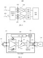
- FIG. 1 illustrates a block diagram of an example coherent optical receiver 100 to which embodiments of the present disclosure may relate.
- An optical signal 101 received from an optical communication link (not shown) is mixed with local oscillator (LO) light 103 in an optical hybrid 115.
- LO local oscillator
- Different mixtures of the optical signal and LO light from four output ports of the optical hybrid are transmitted to two serially connected, photodiode (PD) pairs 120.
- PD photodiode
- Each serially connected pair of PDs 120 may be suitably biased.
- the two PDs of a pair 120 measure mixtures of the received optical signal light 101 with LO light 103 with different relative phase shifts.
- the signals from the two PDs of a pair 120 are coupled to the differential inputs of a corresponding trans-impedance amplifier (TIA) 130.
- TIA trans-impedance amplifier
- Differential outputs of the TIAs 130 are provided to respective ADCs 140, which are, in turn, connected to
- FIG. 2 A block diagram of a typical TIA circuit 200, which may be implemented e.g. as an Application-Specific Integrated Circuit (ASIC), is shown in FIG. 2 . It includes a front-end TIA (FE-TIA) 210, which converts PD current(s) I INp , I INn from a PD pair 120 into a voltage signal, followed by a series of one or more Variable Gain Amplifiers (VGA) 220 to provide further voltage amplification, and an output driver 230.
- the output driver 230 is typically a transconductor, which drives an on-chip termination resistor 240 as well as being connected to the inputs of the ADC.
- the TIA circuit 200 may also include a peak detector 250 to measure the output swing, and an Automatic Gain Control (AGC) loop 260, which adjusts the TIA gain in order to keep the peak output swing at a desired value in the presence of slow variations of the swing of the currents I INp , I INn input to the TIA circuit 200.
- AGC Automatic Gain Control
- the amplitude of an input signal to each TIA 130 can vary by an order of magnitude (20dB) or more due to events in the optical network. Such events can substantially change the optical signal propagating to an optical receiver, typically at a rate much lower than the baud rate or symbol rate of the optical signal 101.
- gain of the TIA circuit 200 may be adjusted by the AGC 260, so that the amplitude of the output signal remains about constant and remains within a desirable operating range of the ADC 140 connected to receive the output signals V OUTp , V OUTn of the TIA circuit 200.
- Gain adjustment in a TIA circuit may be done in part using one or more VGAs 220 that typically follow the FE-TIA in the TIA's signal processing chain, as illustrated in FIG. 2 .
- a VGA is designed to vary the signal gain while keeping other performance metrics (bandwidth, noise, linearity) as constant as possible.
- bandwidth, noise, linearity bandwidth, noise, linearity
- output-referred linear range means a range of output voltage amplitude values within which an output signal is an approximately linear function of the input signal.
- approximately linear means linear with accuracy suitable for a particular application, as typically specified by a selected nonlinearity measure of the amplifier signal response being smaller than a threshold value, e.g., the quantization of measured values by a ADC.
- a threshold value e.g., the quantization of measured values by a ADC.
- the amplifier operation may be referred to as “approximately linear” when a total harmonic distortion (THD) of the output signal is smaller than a specified threshold value, e.g. less than 5%, or less than 2% in some embodiments.
- TDD total harmonic distortion
- input-referred linear range means a range of input voltage amplitude values within which the amplifier response is approximately linear as defined above.
- An AGC feedback loop can adjust the signal gain in a manner that ensures that the TIA circuit output swing remains about constant at a target amplitude value, irrespective of much longer time-scale variations in the average input signal amplitude.
- the output signal amplitude should desirably remain within the amplifier's approximate linear range in the presence of changes to the TIA gain.
- VGA output DC bias should not vary significantly with gain.
- the signal processing chain of the TIA circuit is typically DC coupled, a variation of the DC bias might have a detrimental effect on the operation of the subsequent amplifier blocks.
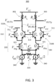
- FIG. 3 illustrates an example VGA 300 that may be used in a TIA circuit such as TIA 200, e.g. for high-speed TIAs.
- the VGA 300 has a differential cascode topology and includes current steering circuits 310A, 310B for gain tuning. At maximum gain, transistors 311(labeled Q 5 and Q 6 in FIG. 3 ) of the current steering circuits 310A and 310B are turned off by setting a base voltage bias V bn to a value significantly lower than a base voltage bias V bp , e.g.
- the current steering circuits 310A, 310B may be commonly referred to as the current steering structure 310.
- the common-mode DC signal at the output of the VGA 300 e.g the DC current I DC,RL through the load resistors(s) R L 303, varies as the fraction of the DC current from the transistors 321, Q 1 and Q 2 , that is steered to the load 303 changes, hence the output DC bias varies with gain.
- linear range the range in which the transfer characteristic of the circuit of FIG. 3 remains approximately linear
- I EE is the tail DC current of the input stage 320 of the VGA 300, i.e. of the Q 1 /Q 2 transistor pair, and the emitter degeneration resistor 335, with the degeneration resistance value R E .
- the VGA 300 of FIG. 3 includes one or more variable current sources 340 for varying the tail DC current I EE .
- the tail DC current I EE may be varied in response to, or in parallel with, varying the base voltage V bn , so as to keep the DC current I DC,RL through the load resistor(s) R L 303 approximately constant over a target range of the VGA gain variations. Furthermore, keeping the DC current through the load resistor(s) R L 303 approximately constant may also lessen the degradation of the output-referred linear range of the VGA 300 at low gain.
- both the signal (AC) and DC current through transistors 313, Q 3 and Q 4 is reduced k times by suitably varying the base voltage V bn , or the base voltage difference (V bn -V bp ), to steer the remaining current through the transistors 311, Q 5 and Q 6 .
- I EE is increased by k times.
- the resistance R E of the degeneration resistor 335, and the capacitance C E of a capacitor 325 when present, may have constant values independent on the VGA gain.
- one or more VGA stage(s) may be used as an equalizer to somewhat expand the BW of the FE-TIA (e.g. 210, FIG. 2 ).
- the capacitor C E 325 is typically placed between the emitters of the transistors 321, Q 1 and Q 2 , in parallel with the resistor R E 335, to create some amount of high-frequency peaking. The amount of peaking is a function of the R E *C E product.
- the tuning of the VGA gain in the embodiment of FIG. 3 may be performed by tuning the source(s) 340 of the tail DC current I EE , without tuning either the R E or the C E .
- the value R E of the degeneration resistor 335 may be selected so that R E ⁇ 1 / gm Q12 .
- gm Q12 is the transconductance of the transistors 321, Q 1 and Q 2 , which may depend on the tail DC current I EE .
- Linear transconductors employing bipolar devices such as the ones used in most high-speed TIAs, are known to use resistive degeneration with R E >>1/gm.
- the product (R E ⁇ gm) may be about or greater than 5, or preferably about or greater than 10, e.g. in a range between 10 and 100.
- the linear range of the VGA 300 may also be affected by transistors Q 3 /Q 4 /Q 5 /Q 6 , whose linearity may decrease at low gain.
- this is a second-order effect, and the dominant contribution to linearity distortion is typically the input differential pair 320.
- the example VGA circuit 300 of FIG. 3 may not achieve a perfectly constant output linear range, the VGA circuit 300 of FIG. 3 is expected to enable lessening the sensitivity of the output linear range to VGA gain setting compared to some conventional current-steering amplifiers.
- the tail DC current I EE may be adjusted by an external controller 410 that is configured to vary, e.g. the base voltages V bn , and possibly V bp , simultaneously with controlling the tail current source(s) 340 to vary the tail DC current I EE so as to keep the DC current I DC_RL through the load resistor(s) R L 303 constant.
- the controller 410 may include memory 420 storing a look-up table (LUT) relating VGA gain setting to the V bn and I EE values.
- LUT look-up table
- FIG. 6 shows an example circuit 600 that may be used to generate the bias voltages V bp , V bn of the current steering circuits 310A, 310B in the TIA circuits of FIG. 3 , FIG. 4 , or FIG. 5 .
- Transistors Q 7 and Q 8 function as a replica of the transistors Q 3 /Q 4 and the transistors Q 5 /Q 6 , respectively (see FIG. 3 ).
- the ratio between currents I GCp and I GCn sets the ratio of the current flowing through the main signal path in the VGA 300 (the transistors Q 3 /Q 4 ) to the current through the dummy path (the transistors Q 5 /Q 6 ), and therefore also sets the VGA gain.
- the tail current source 340 may be implemented, e.g., with a transistor combined with an emitter degeneration resistance, as typically done for bipolar current sources. However the emitter degeneration resistance within the current source affects primarily the DC current I EE from the source, and approximately does not affect an AC transconductance of the input stage 320 (the input differential transistor pair Q 1 , Q 2 in FIGs. 3 and 4 ).
- FIGs. 7, 8, and 9 illustrate example circuit implementations of the variable tail current source(s) 340 shown in FIGs. 3-5 .
- a variable DC current I EE may be tuned by tuning a control voltage V CTRL .
- One option is to use a voltage-controlled-current source (VCCS) 710 followed by a multiplying current mirror 720 (transistors Q 1 and Q 2 in FIG. 7 ), as illustrated in FIG. 7 .
- the VCCS 710 implemented for example as a degenerated differential pair with a diode-connected load, compares the control voltage V CTRL to a reference voltage V REF , to provide a tunable current I B to the current mirror 720.
- the current I B is approximately linearly proportional to a voltage difference (V CTRL -V REF ).
- the voltage V CTRL is used to control the base of a degenerated bipolar transistor Q 3 . Since the base-emitter voltage V BE of a bipolar transistor is approximately constant versus collector current variations, the current I EE is approximately given by (V CTRL -V BE )/R D .
- the current source of FIG. 9 includes a current mirror with variable degeneration resistance (transistor M D ), biased with a fixed current I BB .
- the reference transistor of the mirror (Q 4 ) is degenerated by a fixed resistor R L
- the output transistor (Q 5 ) is degenerated by a variable resistor, e.g. implemented with a FET transistor M D biased in the triode region, whose source-drain resistance is a function of gate voltage V CTRL .
- the ratio I EE /I BB is approximately given by the ratio between resistor R L and the source-drain resistance of M D , which in turn is a function of V CTRL
- the example embodiments illustrated in FIGs. 3 , 4 , and 5 have a differential input to differential output configuration
- other embodiments may have single input to differential output configuration, single input to single output (SISO) configuration, or a differential input to single output configuration.
- SISO single input to single output
- the degeneration resistor 335 may be connected between the emitter of the input transistor Q 1 and a capacitor creating an AC short to ground, or a voltage source replicating the DC bias point at the emitter of Q 1 , so that only AC current and no DC current flows through the degeneration resistor 335 R E .
- the VGA may use one individual current source generating current IEE, connected to the mid-point of resistor 335 R E .
- other gain variation techniques such as tuning degeneration resistor 335 R E or load resistor 303 R L , may be added in addition to current steering to extend the gain range of the VGA.
- any of the bipolar transistors from FIG. 3 , FIG. 4 , and FIG. 5 may be replaced with a FET transistor.
- degeneration capacitor 325 C E may be omitted, or may be made tunable.
- the proposed VGA may be used as a core amplification stage of a transimpedance amplifier (e.g. the FE-TIA block in FIG. 2 ), e.g. adding a feedback resistor between the outputs and inputs of the VGA.
- a transimpedance amplifier e.g. the FE-TIA block in FIG. 2
Landscapes
- Engineering & Computer Science (AREA)
- Power Engineering (AREA)
- Physics & Mathematics (AREA)
- Electromagnetism (AREA)
- Amplifiers (AREA)
Abstract
An apparatus, e.g. an optical signal receiver, includes a trans-impedance amplifier (TIA) circuit. The TIA circuit includes a variable gain amplifier (VGA) having a tunable tail current source (340). The TIA circuit is configured to tune the tail current source (340) to stabilize a DC current to a load resistor (303) of the VGA over an operating gain range of the TIA circuit.
Description
- Various example embodiments relate to circuits and methods for trans-impedance amplifiers and optical receivers using trans-impedance amplifiers.
- Trans-impedance amplifiers (TIAs) are used in high speed fiber optic communication systems. TIAs provide a link between the optical-to-electrical photo detectors (PD), and the downstream electronics. A TIA converts the current coming from the PD into a voltage, thus providing transimpedance gain (ZT). This voltage is typically fed to an ADC, and the resulting signal may be processed in the digital domain. The TIA is desirably linear and has a well-controlled gain, in the relevant operating range, so that the ADC receives a voltage that is a linear representation of the current from the PD and has a magnitude that matches the dynamic range of the ADC.
- An aspect of the present disclosure provides an apparatus. Embodiments of the apparatus comprise a trans-impedance amplifier (TIA) circuit, the TIA circuit comprising a variable gain amplifier (VGA). The VGA is configured to tune a tail current source to stabilize a DC current to a load resistor of the VGA over an operating gain range of the TIA circuit.
- In any of the above embodiments, the VGA may comprise an amplification stage and a current steering structure to selectably steer a fraction of the current output by the amplification stage to the load resistor. The VGA may be operable to cause the structure to vary said fraction.
- Any of the above embodiments may comprise a controller configured to increase a DC current from the tail current source in response to a fraction of an electrical current flowing to the load resistor decreasing.
- Some of the above embodiments may comprise a feedback loop configured to adjust the tail current source by comparing an output DC voltage of the VGA to a reference voltage. In any of such embodiments, the feedback loop may be configured to maintain an output DC voltage of the VGA substantially constant. In some of such embodiments, the VGA may have differential outputs, with the output DC voltage being a common mode voltage.
- In any of the above embodiments, the VGA may be a differential VGA comprising two current-steering circuits connecting to a differential amplification stage, the differential amplification stage connecting to one or more variable current sources.
- In some of the above embodiments, the VGA may comprise the tail current source and the load resistor. Some of such embodiments may comprise a feedback loop configured to adjust the tail current source responsive to an output DC voltage of the VGA and a reference voltage. In some of such embodiments, the VGA may have differential outputs, with the DC output voltage being a common mode voltage, and the feedback loop may be configured to compare the DC output voltage to a reference voltage. In some of such embodiments, the VGA comprises an amplification stage and the tail current source, the tail current source being tunable by the feedback loop to vary a DC electrical current biasing the amplification stage.
- Any of the above embodiments may comprise a coherent optical receiver including a photodetector pair, wherein the output of each photodiode is connected to an input of the TIA circuit.
- An aspect of the present disclosure provides a method for operating a TIA circuit, comprising: varying a gain of an VGA of the TIA circuit; and tuning a tail current source of the VGA to stabilize a DC current to a load resistor of the VGA over an operating gain range of the TIA circuit. Some embodiments of the method may comprise steering a fraction of a current output by an amplification stage of the VGA to the load resistor, and varying said fraction to vary the gain of the VGA.
- Embodiments disclosed herein will be described in greater detail with reference to the accompanying drawings which represent preferred embodiments thereof, in which like elements are indicated with like reference numerals, and wherein:
-
FIG. 1 is a schematic block diagram of a coherent optical receiver where the TIA(s) of the present disclosure may be used; -
FIG. 2 is a schematic block diagram of a TIA circuit that may be used in the coherent optical receiver ofFIG. 1 ; -
FIG. 3 shows a VGA circuit for use in the TIA ofFIG. 1 or FIG. 2 ; -
FIG. 4 shows the VGA circuit ofFIG. 3 with a controller for controlling the tail current source(s) according to an embodiment; -
FIG. 5 is a circuit diagram illustrating the VGA circuit ofFIG. 3 with a closed-loop control of the tail DC current; -
FIG. 6 shows an example base voltage bias circuit for use in the VGA of any of the circuits shown inFIGs. 3 to 5 . -
FIG. 7 shows an example tunable current source including a voltage-controlled current source and a current mirror for use in the VGA of any of the circuits shown inFIGs. 3 to 5 ; -
FIG. 8 shows an example tunable current source including a degenerated bipolar transistor with variable base voltage for use in the VGA of any of the circuits shown inFIGs. 3 to 5 ; -
FIG. 9 shows an example tunable current source including a current source with variable degeneration resistance for use in the VGA of any of the circuits shown inFIGs. 3 to 5 . - In the following description, for purposes of explanation and not limitation, specific details are set forth, such as particular circuits, circuit components, techniques, etc. in order to provide a thorough understanding of the present invention. However, it will be apparent to one skilled in the art that the present invention may be practiced in other embodiments that depart from these specific details. In other instances, detailed descriptions of well-known methods, devices, and circuits may be omitted so as not to obscure the description of the present invention. All statements herein reciting principles, aspects, and embodiments of the invention, as well as specific examples thereof, are intended to encompass both structural and functional equivalents thereof. Additionally, it is intended that such equivalents include both currently known equivalents as well as equivalents developed in the future, i.e., any elements developed that perform the same function, regardless of structure.
- Furthermore, the following abbreviations and acronyms may be used in the present document:
- ADC: Analog to Digital Converter
- AGC: Automatic Gain Control
- Av: voltage gain
- CE: emitter degeneration capacitance
- DSP: Digital Signal Processing
- FET: Field Effect Transistor
- RE: emitter degeneration resistance
- TIA: TransImpedance Amplifier
- VGA: Variable Gain Amplifier
- BW: BandWidth
- ZT: trans impedance
-
FIG. 1 illustrates a block diagram of an example coherentoptical receiver 100 to which embodiments of the present disclosure may relate. Anoptical signal 101 received from an optical communication link (not shown) is mixed with local oscillator (LO)light 103 in anoptical hybrid 115. Different mixtures of the optical signal and LO light from four output ports of the optical hybrid are transmitted to two serially connected, photodiode (PD)pairs 120. Each serially connected pair ofPDs 120 may be suitably biased. The two PDs of apair 120 measure mixtures of the receivedoptical signal light 101 withLO light 103 with different relative phase shifts. The signals from the two PDs of apair 120 are coupled to the differential inputs of a corresponding trans-impedance amplifier (TIA) 130. Differential outputs of the TIAs 130 are provided torespective ADCs 140, which are, in turn, connected to aDSP 150 for signal processing and data demodulation. - A block diagram of a
typical TIA circuit 200, which may be implemented e.g. as an Application-Specific Integrated Circuit (ASIC), is shown inFIG. 2 . It includes a front-end TIA (FE-TIA) 210, which converts PD current(s) I INp, I INn from aPD pair 120 into a voltage signal, followed by a series of one or more Variable Gain Amplifiers (VGA) 220 to provide further voltage amplification, and anoutput driver 230. Theoutput driver 230 is typically a transconductor, which drives an on-chip termination resistor 240 as well as being connected to the inputs of the ADC. TheTIA circuit 200 may also include apeak detector 250 to measure the output swing, and an Automatic Gain Control (AGC)loop 260, which adjusts the TIA gain in order to keep the peak output swing at a desired value in the presence of slow variations of the swing of the currents I INp, I INn input to theTIA circuit 200. - For the coherent
optical receiver 100 illustrated inFIG. 1 , the amplitude of an input signal to eachTIA 130 can vary by an order of magnitude (20dB) or more due to events in the optical network. Such events can substantially change the optical signal propagating to an optical receiver, typically at a rate much lower than the baud rate or symbol rate of theoptical signal 101. In response to such events, gain of theTIA circuit 200 may be adjusted by theAGC 260, so that the amplitude of the output signal remains about constant and remains within a desirable operating range of theADC 140 connected to receive the output signals V OUTp, V OUTn of theTIA circuit 200. - Gain adjustment in a TIA circuit may be done in part using one or
more VGAs 220 that typically follow the FE-TIA in the TIA's signal processing chain, as illustrated inFIG. 2 . Preferably, a VGA is designed to vary the signal gain while keeping other performance metrics (bandwidth, noise, linearity) as constant as possible. In a TIA with an AGC, it is usually desirable to keep an output-referred linear range about constant in light of such gain variations. The term "output-referred linear range" means a range of output voltage amplitude values within which an output signal is an approximately linear function of the input signal. Here, "approximately linear" means linear with accuracy suitable for a particular application, as typically specified by a selected nonlinearity measure of the amplifier signal response being smaller than a threshold value, e.g., the quantization of measured values by a ADC. By way of example, the amplifier operation may be referred to as "approximately linear" when a total harmonic distortion (THD) of the output signal is smaller than a specified threshold value, e.g. less than 5%, or less than 2% in some embodiments. The term "input-referred linear range" means a range of input voltage amplitude values within which the amplifier response is approximately linear as defined above. An AGC feedback loop can adjust the signal gain in a manner that ensures that the TIA circuit output swing remains about constant at a target amplitude value, irrespective of much longer time-scale variations in the average input signal amplitude. The output signal amplitude should desirably remain within the amplifier's approximate linear range in the presence of changes to the TIA gain. - The above-described desirable properties can be challenging to achieve when setting a VGA to an about minimum gain. If we define a target output-referred linear range as Aout,lin and the VGA gain as Av, the VGA input-referred linear range is given by Ain,lin = Aout,lin/Av. As a result, Ain,lin increases inversely proportionally to the gain, resulting in challenging linearity specifications near the minimum gain.
- For example, for a VGA with variable gain between 0dB (1x) and 20dB (10x), at maximum gain Ain,lin= Aout,lin/10, while at minimum gain Ain,lin= Aout,lin.
- Another desirable property is that the VGA output DC bias should not vary significantly with gain. In embodiments where the signal processing chain of the TIA circuit is typically DC coupled, a variation of the DC bias might have a detrimental effect on the operation of the subsequent amplifier blocks.
-
FIG. 3 illustrates anexample VGA 300 that may be used in a TIA circuit such asTIA 200, e.g. for high-speed TIAs. TheVGA 300 has a differential cascode topology and includescurrent steering circuits FIG. 3 ) of thecurrent steering circuits FIG. 3 ). To reduce the gain of theVGA 300, the base voltage Vbn of thetransistors 311, Q5 and Q6, is increased to turn those transistors on, thereby steering a part of the signal current from thetransistors 321, labeled Q1 and Q2 inFIG. 3 , away from theload resistor R L 303. Thecurrent steering circuits current steering structure 310. - If the DC current(s) through the
transistors 321, Q1 and Q2, remain constant when the base voltages Vb change, the common-mode DC signal at the output of theVGA 300, e.g the DC current IDC,RL through the load resistors(s)R L 303, varies as the fraction of the DC current from thetransistors 321, Q1 and Q2, that is steered to theload 303 changes, hence the output DC bias varies with gain. - Furthermore, if the tail current IEE of the
VGA 300 remains constant as the VGA gain is adjusted, the output-referred linear range may degrade at low gain. In some approximation, the range in which the transfer characteristic of the circuit ofFIG. 3 remains approximately linear ("linear range") is mostly set by the input degenerated differential pair transconductor 330 (Q1/Q2/RE), which has an input linear range approximately proportional to RE*IEE, where IEE is the tail DC current of theinput stage 320 of theVGA 300, i.e. of the Q1/Q2 transistor pair, and theemitter degeneration resistor 335, with the degeneration resistance value RE. Here, "tail DC current(s)" refers to the DC current(s) biasing theinput stage 320 of theVGA 300 and sourced from a DC current source ("tail current source") that is connected, e.g. to the emitter(s) (source(s) in FET-based embodiments) of theinput stage 320. Therefore the input linear range Ain,lin is approximately constant over gain, and as a result the output linear range Aout,lin =Av*Ain,lin decreases proportionally to the gain Av. As a second-order effect, the current steering structure 310 (Q3/Q4/Q5/Q6) may also affect the linearity at low gain, so the output linear range is degraded further. - In order to at least partially correct for these drawbacks of a conventional current-steering VGA, the
VGA 300 ofFIG. 3 includes one or more variablecurrent sources 340 for varying the tail DC current IEE. In an embodiment, the tail DC current IEE may be varied in response to, or in parallel with, varying the base voltage Vbn, so as to keep the DC current IDC,RL through the load resistor(s)R L 303 approximately constant over a target range of the VGA gain variations. Furthermore, keeping the DC current through the load resistor(s)R L 303 approximately constant may also lessen the degradation of the output-referred linear range of theVGA 300 at low gain. - By way of example, in order to change the VGA gain by a factor of 1/k through current steering, i.e. reduce k times, k > 1, both the signal (AC) and DC current through
transistors 313, Q3 and Q4, is reduced k times by suitably varying the base voltage Vbn, or the base voltage difference (Vbn-Vbp), to steer the remaining current through thetransistors 311, Q5 and Q6. To keep the DC current through thetransistors 313, Q3 and Q4, constant, IEE is increased by k times. As a result, the input linear voltage range of the input gain stage, which is given approximately by a product IEE*RE, increases by a factor of k. Therefore, the output linear range Aout,lin = A v. Ain,lin of theVGA 300 is approximately independent of k, so that the degradation of the output linear range at low gain values is absent or at least lessened. - Furthermore, in the
VGA 300 ofFIG. 3 the resistance RE of thedegeneration resistor 335, and the capacitance CE of acapacitor 325, when present, may have constant values independent on the VGA gain. In some embodiments, e.g. in high-speed TIAs, one or more VGA stage(s) may be used as an equalizer to somewhat expand the BW of the FE-TIA (e.g. 210,FIG. 2 ). For equalization, thecapacitor C E 325 is typically placed between the emitters of thetransistors 321, Q1 and Q2, in parallel with theresistor R E 335, to create some amount of high-frequency peaking. The amount of peaking is a function of the RE*CE product. As a result, if the resistance RE of theresistor 335 varies versus gain, so typically does high frequency peaking, which is undesired. One possible solution is to make the CE tunable by using a varactor; however, adjusting the value of CE to account for the RE variations may interfere with using the CE tuning as an extra degree of freedom to adjust the amplifier bandwidth, which may also be a desired feature, e.g. in high-speed TIAs. Advantageously, the tuning of the VGA gain in the embodiment ofFIG. 3 may be performed by tuning the source(s) 340 of the tail DC current IEE, without tuning either the RE or the CE. - In an embodiment, the value RE of the
degeneration resistor 335 may be selected so that
transistors 321, Q1 and Q2, which may depend on the tail DC current IEE. The transconductance Gm of the degenerateddifferential transistor pair 320, which is approximately given by Gm = gmQ12/(1+gmQ12*RE), may be approximated as Gm = 1/RE when condition (1) holds, and therefore Gm is approximately independent of the DC current flowing through thedifferential transistor pair 320. Linear transconductors employing bipolar devices, such as the ones used in most high-speed TIAs, are known to use resistive degeneration with RE>>1/gm. By way of example, the product (RE·gm) may be about or greater than 5, or preferably about or greater than 10, e.g. in a range between 10 and 100. - The above description relates to an impact on the VGA linearity by the
input stage 320 of the VGA, i.e. the degenerated differential transistor pair Q1, Q2. In some embodiments the linear range of theVGA 300 may also be affected by transistors Q3/Q4/Q5/Q6, whose linearity may decrease at low gain. However this is a second-order effect, and the dominant contribution to linearity distortion is typically the inputdifferential pair 320. As a result, although theexample VGA circuit 300 ofFIG. 3 may not achieve a perfectly constant output linear range, theVGA circuit 300 ofFIG. 3 is expected to enable lessening the sensitivity of the output linear range to VGA gain setting compared to some conventional current-steering amplifiers. - Referring to
FIG. 4 , in some embodiments (e.g. 400), the tail DC current IEE may be adjusted by anexternal controller 410 that is configured to vary, e.g. the base voltages Vbn, and possibly Vbp, simultaneously with controlling the tail current source(s) 340 to vary the tail DC current IEE so as to keep the DC current IDC_RL through the load resistor(s)R L 303 constant. In an embodiment, thecontroller 410 may includememory 420 storing a look-up table (LUT) relating VGA gain setting to the Vbn and IEE values. - Referring to
FIG. 5 , in some embodiments (e.g. 500), the tail DC current IEE can be adjusted using afeedback loop 510, which includes anoperational amplifier 520 as a comparator, and which keeps an output common-mode DC bias of theVGA 300, VCM,OUT, to be approximately equal to a constant reference voltage VREF. Since the output common-mode voltage is given approximately by VCM,OUT= VCC - RL*IDC,RL, and the RL is largely independent of the VGA gain, adjusting the tail DC current IEE in this manner also ensures that the DC load current IDC,RL is kept about constant as the gain varies. -
FIG. 6 shows anexample circuit 600 that may be used to generate the bias voltages Vbp, Vbn of thecurrent steering circuits FIG. 3 ,FIG. 4 , orFIG. 5 . Transistors Q7 and Q8 function as a replica of the transistors Q3/Q4 and the transistors Q5/Q6, respectively (seeFIG. 3 ). The ratio between currents IGCp and IGCn sets the ratio of the current flowing through the main signal path in the VGA 300 (the transistors Q3/Q4) to the current through the dummy path (the transistors Q5/Q6), and therefore also sets the VGA gain. - The tail
current source 340 may be implemented, e.g., with a transistor combined with an emitter degeneration resistance, as typically done for bipolar current sources. However the emitter degeneration resistance within the current source affects primarily the DC current IEE from the source, and approximately does not affect an AC transconductance of the input stage 320 (the input differential transistor pair Q1, Q2 inFIGs. 3 and4 ). -
FIGs. 7, 8, and 9 illustrate example circuit implementations of the variable tail current source(s) 340 shown inFIGs. 3-5 . In each of these circuits, a variable DC current IEE may be tuned by tuning a control voltage VCTRL. One option is to use a voltage-controlled-current source (VCCS) 710 followed by a multiplying current mirror 720 (transistors Q1 and Q2 inFIG. 7 ), as illustrated inFIG. 7 . TheVCCS 710, implemented for example as a degenerated differential pair with a diode-connected load, compares the control voltage VCTRL to a reference voltage VREF, to provide a tunable current IB to thecurrent mirror 720. In some voltage range around the VREF, the current IB is approximately linearly proportional to a voltage difference (VCTRL-VREF). Thecurrent mirror 720 then outputs the tail current IEE = N*IB, where the multiplication factor N is given by the ratio of transistor emitter lengths and degeneration resistors of the current mirror. - In the current source of
FIG. 8 , the voltage VCTRL is used to control the base of a degenerated bipolar transistor Q3. Since the base-emitter voltage VBE of a bipolar transistor is approximately constant versus collector current variations, the current IEE is approximately given by (VCTRL-VBE)/RD. - The current source of
FIG. 9 includes a current mirror with variable degeneration resistance (transistor MD), biased with a fixed current IBB. Here the reference transistor of the mirror (Q4) is degenerated by a fixed resistor RL, while the output transistor (Q5) is degenerated by a variable resistor, e.g. implemented with a FET transistor MD biased in the triode region, whose source-drain resistance is a function of gate voltage VCTRL. As a result, the ratio IEE/IBB is approximately given by the ratio between resistor RL and the source-drain resistance of MD, which in turn is a function of VCTRL - It will be understood by one skilled in the art that various changes in detail may be affected in the described embodiment without departing from the spirit and scope of the invention as defined by the claims. For example, although the example embodiments illustrated in
FIGs. 3 ,4 , and5 have a differential input to differential output configuration, other embodiments may have single input to differential output configuration, single input to single output (SISO) configuration, or a differential input to single output configuration. In case of a SISO configuration, thedegeneration resistor 335 may be connected between the emitter of the input transistor Q1 and a capacitor creating an AC short to ground, or a voltage source replicating the DC bias point at the emitter of Q1, so that only AC current and no DC current flows through thedegeneration resistor 335 RE. In another example, instead of using two identical tail current sources each generating current IEE/2, as shown inFIG. 3 , the VGA may use one individual current source generating current IEE, connected to the mid-point ofresistor 335 RE. In another example, other gain variation techniques, such as tuning degeneration resistor 335 RE or load resistor 303 RL, may be added in addition to current steering to extend the gain range of the VGA. In another example, any of the bipolar transistors fromFIG. 3 ,FIG. 4 , andFIG. 5 may be replaced with a FET transistor. In another example, degeneration capacitor 325 CE may be omitted, or may be made tunable. In another example, the proposed VGA may be used as a core amplification stage of a transimpedance amplifier (e.g. the FE-TIA block inFIG. 2 ), e.g. adding a feedback resistor between the outputs and inputs of the VGA.
Claims (15)
- An apparatus, comprising:
a trans-impedance amplifier (TIA) circuit (100; 200) comprising a variable gain amplifier (VGA) (220; 300; 400; 500), the VGA configured to tune a tail current source (340; 710, 720) to stabilize a DC current to a load resistor (303) of the VGA over an operating gain range of the TIA circuit. - The apparatus of claim 1, wherein the VGA comprises an amplification stage (320) and a current steering structure (310) to selectably steer a fraction of the current output by the amplification stage to the load resistor; and wherein the VGA is operable to cause the structure to vary said fraction.
- The apparatus of claim 1 or 2, comprising a controller (410) configured to increase a DC current from the tail current source (340) in response to a fraction of an electrical current flowing to the load resistor decreasing.
- The apparatus of claim 1, 2, or 3, comprising a feedback loop (510) configured to adjust the tail current source (340) by comparing an output DC voltage of the VGA to a reference voltage.
- The apparatus of claim 4, wherein the feedback loop is configured to maintain the output DC voltage of the VGA substantially constant.
- The apparatus of any one of claims 1 to 5, wherein the VGA is a differential VGA comprising two current-steering circuits (310A, 310B) connecting to a differential amplification stage (320), the differential amplification stage connecting to one or more variable current sources (340).
- The apparatus of claim 4, wherein the VGA has differential outputs; and wherein the output DC voltage is a common mode voltage.
- The apparatus of claim 7, wherein the VGA is a differential VGA comprising two current-steering circuits (310A, 310B) connecting to a differential amplification stage (320), the differential amplification stage connecting to one or more variable current sources (340).
- The apparatus of any one of claims 1 to 8, wherein the VGA comprises the tail current source and the load resistor.
- The apparatus of claim 2, comprising a feedback loop (510) configured to adjust the tail current source responsive to an output DC voltage of the VGA and a reference voltage.
- The apparatus of claim 10, wherein the VGA has differential outputs, and wherein the feedback loop is configured to compare the DC output voltage to the reference voltage, the DC output voltage being a common mode voltage.
- The apparatus of claim 10, wherein the VGA comprises an amplification stage (320) and the tail current source, the tail current source being tunable by the feedback loop to vary a DC electrical current biasing the amplification stage.
- The apparatus of any one of claims 1 to 12 comprising a coherent optical receiver (100) including a photodetector pair (120) connected to inputs of the TIA circuit.
- A method for operating a trans-impedance amplifier (TIA) circuit, comprising:varying a gain of a variable-gain amplifier (VGA) of the TIA circuit; andtuning a tail current source of the VGA to stabilize a DC current to a load resistor of the VGA over an operating gain range of the TIA circuit.
- The method of claim 14, comprising:steering a fraction of a current output by an amplification stage of the VGA to the load resistor; andvarying said fraction to vary the gain of the VGA.
Applications Claiming Priority (1)
| Application Number | Priority Date | Filing Date | Title |
|---|---|---|---|
| US202263431924P | 2022-12-12 | 2022-12-12 |
Publications (1)
| Publication Number | Publication Date |
|---|---|
| EP4387091A1 true EP4387091A1 (en) | 2024-06-19 |
Family
ID=88923719
Family Applications (1)
| Application Number | Title | Priority Date | Filing Date |
|---|---|---|---|
| EP23211416.5A Pending EP4387091A1 (en) | 2022-12-12 | 2023-11-22 | Method for varying amplifier gain |
Country Status (2)
| Country | Link |
|---|---|
| US (1) | US20240195374A1 (en) |
| EP (1) | EP4387091A1 (en) |
Families Citing this family (2)
| Publication number | Priority date | Publication date | Assignee | Title |
|---|---|---|---|---|
| US20260040958A1 (en) * | 2024-07-31 | 2026-02-05 | Texas Instruments Incorporated | Isolation for chip on lead device and manufacturing method |
| CN119135277B (en) * | 2024-08-30 | 2025-09-30 | 武汉光谷信息光电子创新中心有限公司 | An optical receiver |
Citations (3)
| Publication number | Priority date | Publication date | Assignee | Title |
|---|---|---|---|---|
| JP2015207923A (en) * | 2014-04-22 | 2015-11-19 | 日本電信電話株式会社 | transimpedance amplifier |
| US20190199290A1 (en) * | 2017-12-27 | 2019-06-27 | Qualcomm Incorporated | Differential amplifier with complementary unit structure |
| US10958230B2 (en) * | 2018-09-10 | 2021-03-23 | Elenion Technologies, Llc | Reconfigurable optical receivers with extended dynamic range |
Family Cites Families (2)
| Publication number | Priority date | Publication date | Assignee | Title |
|---|---|---|---|---|
| US5613233A (en) * | 1994-09-30 | 1997-03-18 | Rockwell International Corp. | Apparatus with distortion cancelling feedback signal |
| US10498461B1 (en) * | 2018-09-19 | 2019-12-03 | Elenion Technologies, Llc | Optical receivers with dc cancellation bias circuit and embedded offset cancellation |
-
2023
- 2023-07-21 US US18/356,478 patent/US20240195374A1/en active Pending
- 2023-11-22 EP EP23211416.5A patent/EP4387091A1/en active Pending
Patent Citations (3)
| Publication number | Priority date | Publication date | Assignee | Title |
|---|---|---|---|---|
| JP2015207923A (en) * | 2014-04-22 | 2015-11-19 | 日本電信電話株式会社 | transimpedance amplifier |
| US20190199290A1 (en) * | 2017-12-27 | 2019-06-27 | Qualcomm Incorporated | Differential amplifier with complementary unit structure |
| US10958230B2 (en) * | 2018-09-10 | 2021-03-23 | Elenion Technologies, Llc | Reconfigurable optical receivers with extended dynamic range |
Non-Patent Citations (1)
| Title |
|---|
| AHMED MOSTAFA G ET AL: "34-GBd Linear Transimpedance Amplifier for 200-Gb/s DP-16-QAM Optical Coherent Receivers", IEEE JOURNAL OF SOLID-STATE CIRCUITS, IEEE, USA, vol. 54, no. 3, 21 February 2019 (2019-02-21), pages 834 - 844, XP011711319, ISSN: 0018-9200, [retrieved on 20190222], DOI: 10.1109/JSSC.2018.2882265 * |
Also Published As
| Publication number | Publication date |
|---|---|
| US20240195374A1 (en) | 2024-06-13 |
Similar Documents
| Publication | Publication Date | Title |
|---|---|---|
| US7973602B2 (en) | Variable gain amplifier | |
| JP4032720B2 (en) | Automatic gain control circuit | |
| US7948323B2 (en) | Linear transimpedance amplifier with wide dynamic range for high rate applications | |
| US10622955B2 (en) | Variable gain amplifiers for communication systems | |
| KR100461969B1 (en) | Exponential function generator implemented by CMOS process and variable gain amplifier using the same | |
| US20240195374A1 (en) | Method for varying amplifier gain | |
| US11309845B2 (en) | Reconfigurable optical receivers for extended maximum input signals | |
| EP4387094A1 (en) | Dc voltage regulation and tia with input-output dc voltage control | |
| KR100856131B1 (en) | Variable gain low noise amplifier circuit and wireless communication receiver having same | |
| US7695085B2 (en) | Variable gain amplifier having variable gain DC offset loop | |
| US6753732B1 (en) | Accurate, wide-band, low-noise variable-gain amplifier structures and gain control methods | |
| CA2559169A1 (en) | Highly linear variable gain amplifier | |
| US12316281B2 (en) | Reception circuit for optical communication | |
| US11750162B1 (en) | Variable gain amplifier system including separate bandwidth control based on inductance contribution | |
| EP4387097A1 (en) | Tia with tunable gain | |
| US7319220B2 (en) | Trans-impedance amplifier with offset current | |
| US20240195375A1 (en) | Method for tia transimpedance control | |
| EP1231709A1 (en) | Amplifier | |
| US11855598B2 (en) | Variable gain amplifier including impedance ladder circuit with exponentially dependent degeneration resistance | |
| US12451842B2 (en) | Variable transimpedance amplifier for low power, high dynamic range, high data rate linear | |
| JP2021040208A (en) | Variable gain amplifier and automatic gain control amplifier | |
| US20240195364A1 (en) | Transconductor with current limiter | |
| US20240356504A1 (en) | Transimpedance amplifiers | |
| JP2022171076A (en) | Transimpedance amplifier circuit | |
| US20240195370A1 (en) | Receiver circuit and optical receiver circuit |
Legal Events
| Date | Code | Title | Description |
|---|---|---|---|
| PUAI | Public reference made under article 153(3) epc to a published international application that has entered the european phase |
Free format text: ORIGINAL CODE: 0009012 |
|
| STAA | Information on the status of an ep patent application or granted ep patent |
Free format text: STATUS: THE APPLICATION HAS BEEN PUBLISHED |
|
| AK | Designated contracting states |
Kind code of ref document: A1 Designated state(s): AL AT BE BG CH CY CZ DE DK EE ES FI FR GB GR HR HU IE IS IT LI LT LU LV MC ME MK MT NL NO PL PT RO RS SE SI SK SM TR |
|
| STAA | Information on the status of an ep patent application or granted ep patent |
Free format text: STATUS: REQUEST FOR EXAMINATION WAS MADE |
|
| 17P | Request for examination filed |
Effective date: 20241219 |