EP4387081A2 - Two-switch exciter drive architecture with single switch modes - Google Patents
Two-switch exciter drive architecture with single switch modes Download PDFInfo
- Publication number
- EP4387081A2 EP4387081A2 EP23216434.3A EP23216434A EP4387081A2 EP 4387081 A2 EP4387081 A2 EP 4387081A2 EP 23216434 A EP23216434 A EP 23216434A EP 4387081 A2 EP4387081 A2 EP 4387081A2
- Authority
- EP
- European Patent Office
- Prior art keywords
- switch
- recited
- gate
- gate drive
- exciter
- Prior art date
- Legal status (The legal status is an assumption and is not a legal conclusion. Google has not performed a legal analysis and makes no representation as to the accuracy of the status listed.)
- Pending
Links
Images


Classifications
-
- H—ELECTRICITY
- H02—GENERATION; CONVERSION OR DISTRIBUTION OF ELECTRIC POWER
- H02P—CONTROL OR REGULATION OF ELECTRIC MOTORS, ELECTRIC GENERATORS OR DYNAMO-ELECTRIC CONVERTERS; CONTROLLING TRANSFORMERS, REACTORS OR CHOKE COILS
- H02P7/00—Arrangements for regulating or controlling the speed or torque of electric DC motors
- H02P7/06—Arrangements for regulating or controlling the speed or torque of electric DC motors for regulating or controlling an individual DC dynamo-electric motor by varying field or armature current
- H02P7/18—Arrangements for regulating or controlling the speed or torque of electric DC motors for regulating or controlling an individual DC dynamo-electric motor by varying field or armature current by master control with auxiliary power
- H02P7/24—Arrangements for regulating or controlling the speed or torque of electric DC motors for regulating or controlling an individual DC dynamo-electric motor by varying field or armature current by master control with auxiliary power using discharge tubes or semiconductor devices
- H02P7/28—Arrangements for regulating or controlling the speed or torque of electric DC motors for regulating or controlling an individual DC dynamo-electric motor by varying field or armature current by master control with auxiliary power using discharge tubes or semiconductor devices using semiconductor devices
- H02P7/285—Arrangements for regulating or controlling the speed or torque of electric DC motors for regulating or controlling an individual DC dynamo-electric motor by varying field or armature current by master control with auxiliary power using discharge tubes or semiconductor devices using semiconductor devices controlling armature supply only
- H02P7/29—Arrangements for regulating or controlling the speed or torque of electric DC motors for regulating or controlling an individual DC dynamo-electric motor by varying field or armature current by master control with auxiliary power using discharge tubes or semiconductor devices using semiconductor devices controlling armature supply only using pulse modulation
-
- H—ELECTRICITY
- H02—GENERATION; CONVERSION OR DISTRIBUTION OF ELECTRIC POWER
- H02M—APPARATUS FOR CONVERSION BETWEEN AC AND AC, BETWEEN AC AND DC, OR BETWEEN DC AND DC, AND FOR USE WITH MAINS OR SIMILAR POWER SUPPLY SYSTEMS; CONVERSION OF DC OR AC INPUT POWER INTO SURGE OUTPUT POWER; CONTROL OR REGULATION THEREOF
- H02M5/00—Conversion of AC power input into AC power output, e.g. for change of voltage, for change of frequency, for change of number of phases
- H02M5/02—Conversion of AC power input into AC power output, e.g. for change of voltage, for change of frequency, for change of number of phases without intermediate conversion into DC
- H02M5/04—Conversion of AC power input into AC power output, e.g. for change of voltage, for change of frequency, for change of number of phases without intermediate conversion into DC by static converters
- H02M5/22—Conversion of AC power input into AC power output, e.g. for change of voltage, for change of frequency, for change of number of phases without intermediate conversion into DC by static converters using discharge tubes with control electrode or semiconductor devices with control electrode
- H02M5/275—Conversion of AC power input into AC power output, e.g. for change of voltage, for change of frequency, for change of number of phases without intermediate conversion into DC by static converters using discharge tubes with control electrode or semiconductor devices with control electrode using devices of a triode or transistor type requiring continuous application of a control signal
- H02M5/293—Conversion of AC power input into AC power output, e.g. for change of voltage, for change of frequency, for change of number of phases without intermediate conversion into DC by static converters using discharge tubes with control electrode or semiconductor devices with control electrode using devices of a triode or transistor type requiring continuous application of a control signal using semiconductor devices only
-
- H—ELECTRICITY
- H02—GENERATION; CONVERSION OR DISTRIBUTION OF ELECTRIC POWER
- H02M—APPARATUS FOR CONVERSION BETWEEN AC AND AC, BETWEEN AC AND DC, OR BETWEEN DC AND DC, AND FOR USE WITH MAINS OR SIMILAR POWER SUPPLY SYSTEMS; CONVERSION OF DC OR AC INPUT POWER INTO SURGE OUTPUT POWER; CONTROL OR REGULATION THEREOF
- H02M1/00—Details of apparatus for conversion
- H02M1/08—Circuits specially adapted for the generation of control voltages for semiconductor devices incorporated in static converters
-
- H—ELECTRICITY
- H02—GENERATION; CONVERSION OR DISTRIBUTION OF ELECTRIC POWER
- H02M—APPARATUS FOR CONVERSION BETWEEN AC AND AC, BETWEEN AC AND DC, OR BETWEEN DC AND DC, AND FOR USE WITH MAINS OR SIMILAR POWER SUPPLY SYSTEMS; CONVERSION OF DC OR AC INPUT POWER INTO SURGE OUTPUT POWER; CONTROL OR REGULATION THEREOF
- H02M1/00—Details of apparatus for conversion
- H02M1/08—Circuits specially adapted for the generation of control voltages for semiconductor devices incorporated in static converters
- H02M1/088—Circuits specially adapted for the generation of control voltages for semiconductor devices incorporated in static converters for the simultaneous control of series or parallel connected semiconductor devices
-
- H—ELECTRICITY
- H02—GENERATION; CONVERSION OR DISTRIBUTION OF ELECTRIC POWER
- H02M—APPARATUS FOR CONVERSION BETWEEN AC AND AC, BETWEEN AC AND DC, OR BETWEEN DC AND DC, AND FOR USE WITH MAINS OR SIMILAR POWER SUPPLY SYSTEMS; CONVERSION OF DC OR AC INPUT POWER INTO SURGE OUTPUT POWER; CONTROL OR REGULATION THEREOF
- H02M1/00—Details of apparatus for conversion
- H02M1/32—Means for protecting converters other than automatic disconnection
-
- H—ELECTRICITY
- H02—GENERATION; CONVERSION OR DISTRIBUTION OF ELECTRIC POWER
- H02P—CONTROL OR REGULATION OF ELECTRIC MOTORS, ELECTRIC GENERATORS OR DYNAMO-ELECTRIC CONVERTERS; CONTROLLING TRANSFORMERS, REACTORS OR CHOKE COILS
- H02P25/00—Arrangements or methods for the control of AC motors characterised by the kind of AC motor or by structural details
- H02P25/02—Arrangements or methods for the control of AC motors characterised by the kind of AC motor or by structural details characterised by the kind of motor
- H02P25/08—Reluctance motors
-
- H—ELECTRICITY
- H03—ELECTRONIC CIRCUITRY
- H03K—PULSE TECHNIQUE
- H03K19/00—Logic circuits, i.e. having at least two inputs acting on one output; Inverting circuits
- H03K19/20—Logic circuits, i.e. having at least two inputs acting on one output; Inverting circuits characterised by logic function, e.g. AND, OR, NOR, NOT circuits
Definitions
- the present disclosure relates to exciter drives, and more particularly to two-switch H-bridge topologies.
- GCU Generator control unit
- exciter drive topologies usually consist of a two-switch H-bridge topology in variable frequency (VF) systems, and sometimes in constant frequency (CF) systems, due to the need to quickly remove energy from the exciter field in fault conditions to prevent overvoltage on the generator output.
- the two-switch topology allows for exciter current rate of change that is proportional to the DC link power supply voltage (typically 100-300 Volts) during the off-time rather than a rate of change that is only proportional to a flyback diode forward voltage as in a single-switch topology.
- This two-switch topology allows for energy removal from the exciter field much more quickly than with the single-switch topology, but the two-switch topology has the undesired consequence of additional power dissipation in the additional flyback diode and additional switching transistor.
- a system includes a two-switch H-bridge topology, which has a first switch with a first gate drive connected to control on and off states of the first switch.
- a second switch has a second gate drive connected to control on and off states of the second switch.
- a first flyback diode is connected in series between an exciter load negative side node and a voltage supply line.
- a second flyback diode is connected in series between an exciter load positive node and a voltage return line.
- the first and second flyback diodes are each oriented to provide a flyback current path.
- An exciter winding is connected from a first node between the first switch and the second flyback diode to a second node between the first flyback diode and the second switch.
- a controller is connected to control the first gate drive and the second gate drive in a mode wherein the first switch is always on while the second cycles as a duty-cycle-controlled switch element for the exciter winding.
- a first transformer can have a primary winding operatively coupled to energize a secondary winding.
- the secondary winding can be operatively connected to the first gate drive.
- the secondary winding can connect between the first gate drive and the first node.
- a second transformer can have a primary winding operatively coupled to energize a secondary winding.
- the secondary winding of the second transformer can be operatively connected to the second gate drive.
- the secondary winding of the second transformer can connect between the second gate drive and the return line.
- a first AND gate can be connected to control the first gate drive.
- the first AND gate can have a first input for a carrier signal, and a second input for a first pulse width modulation (PWM) command.
- PWM pulse width modulation
- the first AND gate can connect to a first terminal of the primary winding of the first transformer through a first amplifier.
- the first AND gate can connect to a second terminal of the primary winding of the first transformer through a first inverting amplifier.
- a second AND gate can be connected to control the second gate drive.
- the second AND gate can have a first input for the carrier signal and a second input for a second PWM command.
- the second AND gate can connect to a first terminal of the primary winding of the second transformer through a second amplifier.
- the second AND gate can connect to a second terminal of the primary winding of the second transformer through a second inverting amplifier.
- the controller can include machine readable instructions configured to cause the controller to perform methods as disclosed herein.
- a method includes driving an exciter with a two-switch h-bridge topology having a first switch and a second switch. Driving the exciter includes leaving the first switch on and controlling the second switch as a duty-cycle-controlled switch element.
- the method can include switching the first switch to off during a fault.
- the method can include changing modes so the second switch remains on while the first switch acts as the duty-switch-cycle-controlled switch element.
- the method can include changing modes between having the first switch or the second switch acting as the duty-switch-cycle-controlled switch element. Changing modes can be performed to manage thermal performance of the two-switch h-bridge topology.
- FIG. 1 a partial view of an embodiment of a system in accordance with the disclosure is shown in Fig. 1 and is designated generally by reference character 100.
- FIGs. 2-5 Other embodiments of systems in accordance with the disclosure, or aspects thereof, are provided in Figs. 2-5 , as will be described.
- the systems and methods described herein can be used to provide one switch operation of a two-switch H-bridge topology, with fault protection and thermal management functions.
- a system 100 includes a two-switch H-bridge topology 102 in which a first switch Q1 has a first gate drive 104 connected to control on and off states of the first switch Q1.
- a second switch Q2 has a second gate drive 106 connected to control on and off states of the second switch Q2.
- a first flyback diode D1 is connected in series between the exciter load negative side 110 and a voltage supply line 108.
- a second flyback diode D2 is connected in series between the exciter load positive node 114 and a voltage return line 112, e.g. which connects to the return line Vreturn.
- Both flyback diodes D1 and D2 are oriented to provide a flyback current path when current is interrupted from flowing from the first switch Q1 from the supply line 108 to the exciter load Lexc and Rexc and through the second switch Q2 to the voltage return line 112.
- An exciter winding with inductance Lexc, and resistance Rexc, is connected from the node 114 between the first switch Q1 and the second flyback diode D2 to the node 110 between the first flyback diode D1 and the second switch Q1.
- a controller 116 is connected to control the first gate drive 104 and the second gate drive 106 in a mode wherein one of the switches Q1, Q2 is always on while the second switch Q1, Q2 cycles as a duty-cycle-controlled switch element for the exciter winding Lexc and Rexc.
- a first transformer T1 has a primary winding 118 operatively coupled to energize a first gate drive through T1 secondary winding 120.
- the T1 secondary winding 120 is operatively connected to the first gate drive 104.
- the T1 secondary winding 120 connects between the first gate drive 104 and the exciter load positive node 114.
- a second transformer T2 has a primary winding 122 operatively coupled to energize a second gate drive through T2 secondary winding 124.
- the T2 secondary winding 124 is operatively connected to the second gate drive 106.
- the T2 secondary winding 124 connects between the second gate drive 106 and the return line 112.
- a first AND gate 126 is connected to control the first gate drive 104.
- the first AND gate 126 has a first input 128 for a carrier signal, and a second input 130 for a first pulse width modulation (PWM) command.
- PWM pulse width modulation
- the first AND gate 126 connects to a first terminal 132 of T1 primary winding 118 through a first amplifier U1.
- the first AND gate 126 connects to a second terminal 134 of the T1 primary winding 118 through a first inverting amplifier U2.
- a second AND gate 136 is connected to control the gate drive 106.
- the second AND gate 136 has a first input 138 for the carrier signal and a second input 140 for a second PWM command.
- the second AND gate 136 connects to a first terminal 142 of the T2 primary winding 122 through a second amplifier U3.
- the second AND gate 136 connects to a second terminal 144 of the T2 primary winding 122 through a second inverting amplifier U4.
- the controller 116 is connected to the AND gates 126, 136 to provide the carrier signal and first and second PWM commands, and includes machine readable instructions configured to cause the controller to perform methods as disclosed herein.
- a method includes driving an exciter, e.g. exciter winding Lexc and Rexc, with a two-switch h-bridge topology 102 as described above.
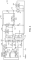
- Driving the exciter includes leaving the first switch, e.g. switch Q1, on and controlling the second switch, e.g. switch Q2, as a duty-cycle-controlled switch element. Referring two Figs. 2 and 4 , this would involve keeping the first PWM command at a logic high as shown in Figs. 2 and 4 , while alternating the second PWM command between logic high and logic low, switching between the states shown in Figs. 2 and 4 .
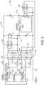
- the second switch Q2 as the always on switch, and the first switch Q1 as the duty-cycle-controlled switch element. Referring to Figs. 2 and 5 , this would involve keeping the second PWM command at a logic high as shown in Figs. 2 and 5 , and alternating the first PWM command between logic high and logic low, switching between the states shown in Figs. 2 and 5 .
- the method can include switching the first switch to off during a fault, e.g. sending a logic low to whichever of the switches is acting as the always on switch, or sending the PWM command for a logic low to both switches as shown in Fig. 3 .
- the method can include changing modes, so the second switch remains on while the first switch acts as the duty-switch-cycle-controlled switch element. For example, in a first mode the first switch Q1 is the always on switch, and in a second mode the second switch Q2 is the always on switch.
- the method can include changing modes between having the first switch or the second switch acting as the duty-switch-cycle-controlled switch element. Changing modes can be performed to manage thermal performance of the two-switch h-bridge topology.
- the state shown in Fig. 3 allows energy to be removed quickly from the exciter field of the exciter winding Lexc and Rexc.
- the state shown in Fig. 4 allows the flyback diode D2 to avoid dissipating power during the off time of the switch Q2 and allows the first switch Q1 to avoid switching losses by remaining closed (on) during the off time of the second switch Q2, reducing power dissipation in the exciter drive.
- the state shown in Fig. 5 allows the flyback diode D1 to avoid dissipating power during the off time of the first switch Q1 and allows the second switch to avoid switching losses by remaining closed (on) during the off time of the first switch Q1, reducing power dissipation in the exciter drive.
- Systems and methods as disclosed herein allow for the switching transistors Q1 and Q2 to be controlled independently to allow for a new state 3 (Q1 on, Q2 off shown in Fig. 4 ) and a new state 4 (Q1 off, Q2 on, shown in Fig. 5 ).
- the exciter drive can reduce total power dissipation and operate more efficiently than a standard two-switch exciter drive, which alternates between states 1&2 (alternating between Fig. 2 and Fig. 3 with Q1 and Q2 both switching).
- Alternating between stares 1&3 or states 1&4 is similar in total power dissipation to a single-switch exciter drive, with only one switching transistor and one flyback diode.
- An additional control concept which can more evenly distribute power dissipation in the exciter drive circuitry during single-switch mode is to operate for some time alternating between states 1&3 (Q1 on, Q2 switching), then operate for some time alternating between Mode 1&4 (Q1 switching, Q2 on).
- the timing of the switching between these two modes 1&3 and 1&4 can be optimized for thermal performance. There are conditions when state 2 of Fig. 3 is still needed, so the controller 116 can use these considerations to determine which modes and states to use at any given time: state 2 ( Fig.
- state 2 ( Fig. 3 ) is needed during overvoltage fault conditions when exciter energy must be removed quickly; and state 2 ( Fig. 3 ) may be needed during high-speed conditions and/or low exciter current conditions when exciter supply voltage Vsupply (in line 108) is larger and generator gain is larger, which causes the control duty cycle to be very small for single-switch mode, which can cause missed switching cycles, which can cause increased modulation in the generator output voltage.
Landscapes
- Engineering & Computer Science (AREA)
- Power Engineering (AREA)
- Power Conversion In General (AREA)
- Dc-Dc Converters (AREA)
Abstract
Description
- The present disclosure relates to exciter drives, and more particularly to two-switch H-bridge topologies.
- Generator control unit (GCU) exciter drive topologies usually consist of a two-switch H-bridge topology in variable frequency (VF) systems, and sometimes in constant frequency (CF) systems, due to the need to quickly remove energy from the exciter field in fault conditions to prevent overvoltage on the generator output. The two-switch topology allows for exciter current rate of change that is proportional to the DC link power supply voltage (typically 100-300 Volts) during the off-time rather than a rate of change that is only proportional to a flyback diode forward voltage as in a single-switch topology. This two-switch topology allows for energy removal from the exciter field much more quickly than with the single-switch topology, but the two-switch topology has the undesired consequence of additional power dissipation in the additional flyback diode and additional switching transistor.
- The conventional techniques have been considered satisfactory for their intended purpose. However, there is an ever present need for improved systems and methods for exciter drives. This disclosure provides a solution for this need.
- A system includes a two-switch H-bridge topology, which has a first switch with a first gate drive connected to control on and off states of the first switch. A second switch has a second gate drive connected to control on and off states of the second switch. A first flyback diode is connected in series between an exciter load negative side node and a voltage supply line. A second flyback diode is connected in series between an exciter load positive node and a voltage return line. The first and second flyback diodes are each oriented to provide a flyback current path. An exciter winding is connected from a first node between the first switch and the second flyback diode to a second node between the first flyback diode and the second switch. A controller is connected to control the first gate drive and the second gate drive in a mode wherein the first switch is always on while the second cycles as a duty-cycle-controlled switch element for the exciter winding.
- A first transformer can have a primary winding operatively coupled to energize a secondary winding. The secondary winding can be operatively connected to the first gate drive. The secondary winding can connect between the first gate drive and the first node. A second transformer can have a primary winding operatively coupled to energize a secondary winding. The secondary winding of the second transformer can be operatively connected to the second gate drive. The secondary winding of the second transformer can connect between the second gate drive and the return line.
- A first AND gate can be connected to control the first gate drive. The first AND gate can have a first input for a carrier signal, and a second input for a first pulse width modulation (PWM) command. The first AND gate can connect to a first terminal of the primary winding of the first transformer through a first amplifier. The first AND gate can connect to a second terminal of the primary winding of the first transformer through a first inverting amplifier.
- A second AND gate can be connected to control the second gate drive. The second AND gate can have a first input for the carrier signal and a second input for a second PWM command. The second AND gate can connect to a first terminal of the primary winding of the second transformer through a second amplifier. The second AND gate can connect to a second terminal of the primary winding of the second transformer through a second inverting amplifier. The controller can include machine readable instructions configured to cause the controller to perform methods as disclosed herein.
- A method includes driving an exciter with a two-switch h-bridge topology having a first switch and a second switch. Driving the exciter includes leaving the first switch on and controlling the second switch as a duty-cycle-controlled switch element.
- The method can include switching the first switch to off during a fault. The method can include changing modes so the second switch remains on while the first switch acts as the duty-switch-cycle-controlled switch element. The method can include changing modes between having the first switch or the second switch acting as the duty-switch-cycle-controlled switch element. Changing modes can be performed to manage thermal performance of the two-switch h-bridge topology.
- These and other features of the systems and methods of the subject disclosure will become more readily apparent to those skilled in the art from the following detailed description of the preferred embodiments taken in conjunction with the drawings.
- So that those skilled in the art to which the subject disclosure appertains will readily understand how to make and use the devices and methods of the subject disclosure without undue experimentation, preferred embodiments thereof will be described in detail herein below with reference to certain figures, wherein:
-
Fig. 1 is a schematic view of an embodiment of a system constructed in accordance with the present disclosure, showing the two-switch H-bridge topology; -
Fig. 2 is a schematic view of the system ofFig 1 , showing both of the switches in the ON state; -
Fig. 3 is a schematic view of the system ofFig. 1 , showing both of the switches in the OFF state; -
Fig. 4 is a schematic view of the system ofFig. 1 , showing flyback with the first switch in the ON state and the second switch in the OFF state; and -
Fig. 5 is a schematic view of the system ofFig. 1 , showing flyback with the second switch in the ON state and the first switch in the OFF state. - Reference will now be made to the drawings wherein like reference numerals identify similar structural features or aspects of the subject disclosure. For purposes of explanation and illustration, and not limitation, a partial view of an embodiment of a system in accordance with the disclosure is shown in
Fig. 1 and is designated generally byreference character 100. Other embodiments of systems in accordance with the disclosure, or aspects thereof, are provided inFigs. 2-5 , as will be described. The systems and methods described herein can be used to provide one switch operation of a two-switch H-bridge topology, with fault protection and thermal management functions. - A
system 100 includes a two-switch H-bridge topology 102 in which a first switch Q1 has afirst gate drive 104 connected to control on and off states of the first switch Q1. A second switch Q2 has asecond gate drive 106 connected to control on and off states of the second switch Q2. A first flyback diode D1 is connected in series between the exciter loadnegative side 110 and avoltage supply line 108. A second flyback diode D2 is connected in series between the exciter loadpositive node 114 and avoltage return line 112, e.g. which connects to the return line Vreturn. Both flyback diodes D1 and D2 are oriented to provide a flyback current path when current is interrupted from flowing from the first switch Q1 from thesupply line 108 to the exciter load Lexc and Rexc and through the second switch Q2 to thevoltage return line 112. An exciter winding with inductance Lexc, and resistance Rexc, is connected from thenode 114 between the first switch Q1 and the second flyback diode D2 to thenode 110 between the first flyback diode D1 and the second switch Q1. - A
controller 116 is connected to control thefirst gate drive 104 and thesecond gate drive 106 in a mode wherein one of the switches Q1, Q2 is always on while the second switch Q1, Q2 cycles as a duty-cycle-controlled switch element for the exciter winding Lexc and Rexc. - A first transformer T1 has a
primary winding 118 operatively coupled to energize a first gate drive through T1secondary winding 120. The T1secondary winding 120 is operatively connected to thefirst gate drive 104. The T1secondary winding 120 connects between thefirst gate drive 104 and the exciter loadpositive node 114. A second transformer T2 has aprimary winding 122 operatively coupled to energize a second gate drive through T2secondary winding 124. The T2secondary winding 124 is operatively connected to thesecond gate drive 106. The T2 secondary winding 124 connects between thesecond gate drive 106 and thereturn line 112. - A first AND
gate 126 is connected to control thefirst gate drive 104. The first ANDgate 126 has afirst input 128 for a carrier signal, and asecond input 130 for a first pulse width modulation (PWM) command. The first ANDgate 126 connects to afirst terminal 132 of T1 primary winding 118 through a first amplifier U1. The first ANDgate 126 connects to asecond terminal 134 of the T1 primary winding 118 through a first inverting amplifier U2. - A second AND
gate 136 is connected to control thegate drive 106. The second ANDgate 136 has afirst input 138 for the carrier signal and asecond input 140 for a second PWM command. The second ANDgate 136 connects to afirst terminal 142 of the T2 primary winding 122 through a second amplifier U3. The second ANDgate 136 connects to asecond terminal 144 of the T2 primary winding 122 through a second inverting amplifier U4. Thecontroller 116 is connected to the ANDgates - A method includes driving an exciter, e.g. exciter winding Lexc and Rexc, with a two-switch h-
bridge topology 102 as described above. Driving the exciter includes leaving the first switch, e.g. switch Q1, on and controlling the second switch, e.g. switch Q2, as a duty-cycle-controlled switch element. Referring twoFigs. 2 and4 , this would involve keeping the first PWM command at a logic high as shown inFigs. 2 and4 , while alternating the second PWM command between logic high and logic low, switching between the states shown inFigs. 2 and4 . - It is also possible to use the second switch Q2 as the always on switch, and the first switch Q1 as the duty-cycle-controlled switch element. Referring to
Figs. 2 and5 , this would involve keeping the second PWM command at a logic high as shown inFigs. 2 and5 , and alternating the first PWM command between logic high and logic low, switching between the states shown inFigs. 2 and5 . - The method can include switching the first switch to off during a fault, e.g. sending a logic low to whichever of the switches is acting as the always on switch, or sending the PWM command for a logic low to both switches as shown in
Fig. 3 . The method can include changing modes, so the second switch remains on while the first switch acts as the duty-switch-cycle-controlled switch element. For example, in a first mode the first switch Q1 is the always on switch, and in a second mode the second switch Q2 is the always on switch. The method can include changing modes between having the first switch or the second switch acting as the duty-switch-cycle-controlled switch element. Changing modes can be performed to manage thermal performance of the two-switch h-bridge topology. - The state shown in
Fig. 3 allows energy to be removed quickly from the exciter field of the exciter winding Lexc and Rexc. The state shown inFig. 4 allows the flyback diode D2 to avoid dissipating power during the off time of the switch Q2 and allows the first switch Q1 to avoid switching losses by remaining closed (on) during the off time of the second switch Q2, reducing power dissipation in the exciter drive. The state shown inFig. 5 allows the flyback diode D1 to avoid dissipating power during the off time of the first switch Q1 and allows the second switch to avoid switching losses by remaining closed (on) during the off time of the first switch Q1, reducing power dissipation in the exciter drive. - Systems and methods as disclosed herein allow for the switching transistors Q1 and Q2 to be controlled independently to allow for a new state 3 (Q1 on, Q2 off shown in
Fig. 4 ) and a new state 4 (Q1 off, Q2 on, shown inFig. 5 ). When alternating between states 1&3 (alternating betweenFig. 2 andFig. 4 , Q1 always on, Q2 switching) or between states 1&4 (alternating betweenFig 2 andFig. 5 , Q1 switching, Q2 always on), the exciter drive can reduce total power dissipation and operate more efficiently than a standard two-switch exciter drive, which alternates between states 1&2 (alternating betweenFig. 2 andFig. 3 with Q1 and Q2 both switching). - Alternating between stares 1&3 or states 1&4 is similar in total power dissipation to a single-switch exciter drive, with only one switching transistor and one flyback diode. An additional control concept which can more evenly distribute power dissipation in the exciter drive circuitry during single-switch mode is to operate for some time alternating between states 1&3 (Q1 on, Q2 switching), then operate for some time alternating between Mode 1&4 (Q1 switching, Q2 on). The timing of the switching between these two modes 1&3 and 1&4 can be optimized for thermal performance. There are conditions when state 2 of
Fig. 3 is still needed, so thecontroller 116 can use these considerations to determine which modes and states to use at any given time: state 2 (Fig. 3 ) is needed during overvoltage fault conditions when exciter energy must be removed quickly; and state 2 (Fig. 3 ) may be needed during high-speed conditions and/or low exciter current conditions when exciter supply voltage Vsupply (in line 108) is larger and generator gain is larger, which causes the control duty cycle to be very small for single-switch mode, which can cause missed switching cycles, which can cause increased modulation in the generator output voltage. - The methods and systems of the present disclosure, as described above and shown in the drawings, provide for one switch operation of a two-switch H-bridge topology, with fault protection and thermal management functions. While the apparatus and methods of the subject disclosure have been shown and described with reference to preferred embodiments, those skilled in the art will readily appreciate that changes and/or modifications may be made thereto without departing from the scope of the invention as defined by the claims.
Claims (15)
- A system comprising:a two-switch H-bridge topology including:a first switch (Q1) with a first gate drive (104) connected to control on and off states of the first switch;a second switch (Q2) with a second gate drive (106) connected to control on and off states of the second switch;a first flyback diode (D1) connected in series between an exciter load negative side node and a voltage supply line;a second flyback diode (D2) connected in series between an exciter load positive node and a voltage return line, wherein the first and second flyback diodes are each oriented to provide a flyback current path; andan exciter winding (Lexc, Rexc) connected from a first node between the first switch and the second flyback diode to a second node between the first flyback diode and the second switch; anda controller (116) connected to control the first gate drive and the second gate drive in a mode wherein the first switch is always on while the second cycles as a duty-cycle-controlled switch element for the exciter winding.
- The system as recited in claim 1, further comprising a first transformer (11) having a primary winding (118) operatively coupled to energize a secondary winding (120), wherein the secondary winding is operatively connected to the first gate drive, and optionally wherein the secondary winding connects between the first gate drive and the first node.
- The system as recited in claim 2, further comprising a second transformer having a primary winding operatively coupled to energize a secondary winding, wherein the secondary winding of the second transformer is operatively connected to the second gate drive.
- The system as recited in claim 3, wherein the secondary winding of the second transformer connects between the second gate drive and the return line.
- The system as recited in claim 4, wherein a first AND gate (126) is connected to control the first gate drive, wherein the first AND gate has a first input for a carrier signal, and a second input for a first pulse width modulation, PWM, command.
- The system as recited in claim 5, wherein the first AND gate connects to a first terminal (132) of the primary winding of the first transformer through a first amplifier.
- The system as recited in claim 6, wherein the first AND gate connects to a second terminal (134) of the primary winding of the first transformer through a first inverting amplifier.
- The system as recited in claim 7, wherein a second AND gate (136) is connected to control the second gate drive, wherein the second AND gate has a first input (138) for the carrier signal and a second input (140) for a second PWM command.
- The system as recited in claim 8, wherein the second AND gate connects to a first terminal of the primary winding of the second transformer through a second amplifier, and optionally wherein the second AND gate connects to a second terminal of the primary winding of the second transformer through a second inverting amplifier.
- The system as recited in any preceding claim, wherein the controller (116) includes machine readable instructions configured to cause the controller to switch the first switch to off during a fault.
- The system as recited in any preceding claim, wherein the controller includes machine readable instruction configured to cause the controller to change modes so the second switch remains on while the first switch acts as the duty-switch-cycle-controlled switch element.
- The system as recited in claim 11, wherein the controller includes machine readable instruction configured to cause the controller to change modes between having the first switch or the second switch acting as the duty-switch-cycle-controlled switch element, and optionally wherein the controller includes machine readable instruction configured to cause the controller to change modes to manage thermal performance of the two-switch h-bridge topology.
- A method comprising:
driving an exciter with a two-switch h-bridge topology having a first switch (Q1) and a second switch (Q2), wherein driving the exciter includes leaving the first switch on and controlling the second switch as a duty-cycle-controlled switch element. - The method as recited in claim 13, further comprising switching the first switch to off during a fault.
- The method as recited in claim 13 or 14, further comprising changing modes so the second switch remains on while the first switch acts as the duty-switch-cycle-controlled switch element, and optionally further comprising changing modes between having the first switch or the second switch acting as the duty-switch-cycle-controlled switch element, and further optionally wherein changing modes is performed to manage thermal performance of the two-switch h-bridge topology.
Applications Claiming Priority (1)
| Application Number | Priority Date | Filing Date | Title |
|---|---|---|---|
| US18/080,214 US12519400B2 (en) | 2022-12-13 | 2022-12-13 | Two-switch exciter drive architecture with single switch modes |
Publications (2)
| Publication Number | Publication Date |
|---|---|
| EP4387081A2 true EP4387081A2 (en) | 2024-06-19 |
| EP4387081A3 EP4387081A3 (en) | 2024-09-18 |
Family
ID=89222821
Family Applications (1)
| Application Number | Title | Priority Date | Filing Date |
|---|---|---|---|
| EP23216434.3A Pending EP4387081A3 (en) | 2022-12-13 | 2023-12-13 | Two-switch exciter drive architecture with single switch modes |
Country Status (2)
| Country | Link |
|---|---|
| US (1) | US12519400B2 (en) |
| EP (1) | EP4387081A3 (en) |
Family Cites Families (18)
| Publication number | Priority date | Publication date | Assignee | Title |
|---|---|---|---|---|
| US4297621A (en) * | 1980-10-02 | 1981-10-27 | Sperry Corporation | Cathode ray tube beam deflection amplifier system |
| WO1992013429A1 (en) | 1991-01-23 | 1992-08-06 | Siemens Aktiengesellschaft | Method of controlling a switching device |
| US5166591A (en) * | 1991-12-02 | 1992-11-24 | General Electric Company | Current chopping strategy for generating action in switched reluctance machines |
| GB9412410D0 (en) | 1994-06-21 | 1994-08-10 | Lucas Ind Plc | Control circuit for electrical generator |
| US6850043B1 (en) | 2003-01-30 | 2005-02-01 | Hamilton Sundstrand Corporation | Excessive voltage protector for a variable frequency generating system |
| JP4238871B2 (en) * | 2004-01-30 | 2009-03-18 | 株式会社村田製作所 | Switching power supply |
| US7157887B2 (en) * | 2004-09-08 | 2007-01-02 | Power Paragon, Inc. | Direct amplitude modulation for switch mode power supplies |
| US7336059B2 (en) * | 2005-11-15 | 2008-02-26 | General Electric Company | System and method for charging and discharging a superconducting coil |
| US8054652B2 (en) * | 2007-07-16 | 2011-11-08 | Texas Instruments Incorporated | Systems and methods for off-time control in a voltage converter |
| US7466109B1 (en) | 2008-04-07 | 2008-12-16 | General Electric Company | Systems and methods involving variable speed generators |
| US7952900B2 (en) * | 2008-04-16 | 2011-05-31 | Analog Devices, Inc. | H-bridge buck-boost converter |
| US8970183B2 (en) | 2011-01-14 | 2015-03-03 | Hamilton Sundstrand Corporation | Overvoltage limiter in an aircraft electrical power generation system |
| WO2015016891A1 (en) * | 2013-07-31 | 2015-02-05 | Schneider Electric Solar Inverters Usa, Inc. | Isolated uni-polar transistor gate drive |
| TWI558084B (en) * | 2015-04-17 | 2016-11-11 | Bidirectional power control and dual power module parallel return controller | |
| US9871479B2 (en) | 2016-06-21 | 2018-01-16 | Hamilton Sundstrand Corporation | Fault detection system for isolated two-switch exciter drive gate driver |
| JP6996660B2 (en) * | 2019-03-14 | 2022-01-17 | オムロン株式会社 | Voltage balance circuit for semiconductor devices |
| US11424612B2 (en) | 2019-04-15 | 2022-08-23 | Ge Aviation Systems Llc | Method and apparatus for over voltage protection of a power system |
| US11699966B1 (en) * | 2022-02-11 | 2023-07-11 | Hamilton Sundstrand Corporation | Open flyback diode protection |
-
2022
- 2022-12-13 US US18/080,214 patent/US12519400B2/en active Active
-
2023
- 2023-12-13 EP EP23216434.3A patent/EP4387081A3/en active Pending
Also Published As
| Publication number | Publication date |
|---|---|
| US12519400B2 (en) | 2026-01-06 |
| US20240195314A1 (en) | 2024-06-13 |
| EP4387081A3 (en) | 2024-09-18 |
Similar Documents
| Publication | Publication Date | Title |
|---|---|---|
| US6618274B2 (en) | Synchronous rectifier controller to eliminate reverse current flow in a DC/DC converter output | |
| US10277130B2 (en) | Primary-side start-up method and circuit arrangement for a series-parallel resonant power converter | |
| US6018467A (en) | Resonant mode power supply having an efficient low power stand-by mode | |
| US6154375A (en) | Soft start scheme for resonant converters having variable frequency control | |
| US6552917B1 (en) | System and method for regulating multiple outputs in a DC-DC converter | |
| US6788554B2 (en) | Switched mode power converter having synchronous rectification and secondary side post regulation | |
| US7095638B2 (en) | Controller for complementary switches of a power converter and method of operation thereof | |
| US6711039B2 (en) | Method and apparatus for controlling synchronous rectifiers of a power converter | |
| EP1675252A1 (en) | PWM control apparatus having a standby mode | |
| US6414854B2 (en) | Driving device and method of switching element in power conversion apparatus using current-controlled semiconductor switching element | |
| US7362598B2 (en) | Synchronous rectifier gate drive shutdown circuit | |
| JP2005513984A (en) | Flyback power converter | |
| WO2002067409A2 (en) | Method and circuit reducing reverse currents in synchronous rectifier converter circuit | |
| CA2059457C (en) | Method for minimizing the switching loss in a power switch | |
| US6738266B2 (en) | Switching power supply unit | |
| US8742295B2 (en) | Inverter output rectifier circuit | |
| CN100389536C (en) | DC-DC Converter | |
| CN102906956A (en) | Stored energy dissipating circuits and methods for switched mode power supplies | |
| US12519400B2 (en) | Two-switch exciter drive architecture with single switch modes | |
| JP2009050080A (en) | Snubber circuit | |
| EP3761499B1 (en) | Power converter | |
| WO2004086599A1 (en) | Power supply | |
| JP2003018827A (en) | Switching power unit | |
| US7277305B2 (en) | Power converter | |
| CN114465484B (en) | Voltage converter |
Legal Events
| Date | Code | Title | Description |
|---|---|---|---|
| PUAI | Public reference made under article 153(3) epc to a published international application that has entered the european phase |
Free format text: ORIGINAL CODE: 0009012 |
|
| STAA | Information on the status of an ep patent application or granted ep patent |
Free format text: STATUS: THE APPLICATION HAS BEEN PUBLISHED |
|
| AK | Designated contracting states |
Kind code of ref document: A2 Designated state(s): AL AT BE BG CH CY CZ DE DK EE ES FI FR GB GR HR HU IE IS IT LI LT LU LV MC ME MK MT NL NO PL PT RO RS SE SI SK SM TR |
|
| PUAL | Search report despatched |
Free format text: ORIGINAL CODE: 0009013 |
|
| AK | Designated contracting states |
Kind code of ref document: A3 Designated state(s): AL AT BE BG CH CY CZ DE DK EE ES FI FR GB GR HR HU IE IS IT LI LT LU LV MC ME MK MT NL NO PL PT RO RS SE SI SK SM TR |
|
| RIC1 | Information provided on ipc code assigned before grant |
Ipc: H02P 25/08 20160101ALI20240812BHEP Ipc: H02M 1/08 20060101ALI20240812BHEP Ipc: H01H 47/32 20060101ALI20240812BHEP Ipc: H02P 7/29 20160101AFI20240812BHEP |
|
| STAA | Information on the status of an ep patent application or granted ep patent |
Free format text: STATUS: REQUEST FOR EXAMINATION WAS MADE |
|
| 17P | Request for examination filed |
Effective date: 20250317 |