EP4386979A1 - Tragbare elektronische vorrichtung mit antenne - Google Patents
Tragbare elektronische vorrichtung mit antenne Download PDFInfo
- Publication number
- EP4386979A1 EP4386979A1 EP22883812.4A EP22883812A EP4386979A1 EP 4386979 A1 EP4386979 A1 EP 4386979A1 EP 22883812 A EP22883812 A EP 22883812A EP 4386979 A1 EP4386979 A1 EP 4386979A1
- Authority
- EP
- European Patent Office
- Prior art keywords
- rim
- electronic device
- disposed
- bridge
- wearable electronic
- Prior art date
- Legal status (The legal status is an assumption and is not a legal conclusion. Google has not performed a legal analysis and makes no representation as to the accuracy of the status listed.)
- Pending
Links
Images


Classifications
-
- H—ELECTRICITY
- H01—ELECTRIC ELEMENTS
- H01Q—ANTENNAS, i.e. RADIO AERIALS
- H01Q1/00—Details of, or arrangements associated with, antennas
- H01Q1/27—Adaptation for use in or on movable bodies
- H01Q1/273—Adaptation for carrying or wearing by persons or animals
-
- G—PHYSICS
- G02—OPTICS
- G02C—SPECTACLES; SUNGLASSES OR GOGGLES INSOFAR AS THEY HAVE THE SAME FEATURES AS SPECTACLES; CONTACT LENSES
- G02C11/00—Non-optical adjuncts; Attachment thereof
- G02C11/10—Electronic devices other than hearing aids
-
- H—ELECTRICITY
- H01—ELECTRIC ELEMENTS
- H01Q—ANTENNAS, i.e. RADIO AERIALS
- H01Q1/00—Details of, or arrangements associated with, antennas
- H01Q1/50—Structural association of antennas with earthing switches, lead-in devices or lightning protectors
-
- H—ELECTRICITY
- H01—ELECTRIC ELEMENTS
- H01Q—ANTENNAS, i.e. RADIO AERIALS
- H01Q21/00—Antenna arrays or systems
- H01Q21/30—Combinations of separate antenna units operating in different wavebands and connected to a common feeder system
-
- H—ELECTRICITY
- H01—ELECTRIC ELEMENTS
- H01Q—ANTENNAS, i.e. RADIO AERIALS
- H01Q7/00—Loop antennas with a substantially uniform current distribution around the loop and having a directional radiation pattern in a plane perpendicular to the plane of the loop
-
- H—ELECTRICITY
- H05—ELECTRIC TECHNIQUES NOT OTHERWISE PROVIDED FOR
- H05K—PRINTED CIRCUITS; CASINGS OR CONSTRUCTIONAL DETAILS OF ELECTRIC APPARATUS; MANUFACTURE OF ASSEMBLAGES OF ELECTRICAL COMPONENTS
- H05K1/00—Printed circuits
- H05K1/02—Details
- H05K1/0277—Bendability or stretchability details
Definitions
- Various embodiments of the disclosure relate to a wearable electronic device including an antenna.
- a wearable electronic device is changed in various forms like augmented reality (AR) glass having a glasses form or a head-mounted display (HMD).
- AR augmented reality
- HMD head-mounted display
- the wearable electronic device may transmit and receive various data to and from another electronic device through wireless communication.
- the wearable electronic device may include at least one antenna (e.g., a conductive pattern) in order to perform wireless communication with another electronic device.
- at least one antenna e.g., a conductive pattern
- a wearable electronic device may include augmented reality (AR) glass having a glasses form or smart glass which implements various content in transparent glass (e.g., a lens).
- AR augmented reality
- the wearable electronic device may be constructed to have rims (e.g., glasses frames) and temples (e.g., the temples of glasses) connected thereto by using hinges and to have the temples folded or unfolded with respect to the rims.
- rims e.g., glasses frames
- temples e.g., the temples of glasses
- the mounting space of an antenna e.g., a conductive pattern
- an antenna e.g., a conductive pattern
- the wearable electronic device may have the antenna included in the temples.
- a specific absorption rate (SAR) may be increased, and radiation performance of the antenna may be reduced.
- a wearable electronic device including an antenna (e.g., a conductive pattern or a loop antenna) disposed between first glass and a first rim, in a bridge, and between second glass and a second rim.
- an antenna e.g., a conductive pattern or a loop antenna
- a wearable electronic device may include a bridge, a first rim disposed in a first direction of the bridge and a second rim disposed in a second direction of the bridge which is a direction opposite to the first direction, first glass disposed to have at least a part thereof surrounded by the first rim and second glass disposed to have at least a part thereof surrounded by the second rim, a first temple operatively connected to at least a part of the first rim by using a first hinge part and a second temple operatively connected to at least a part of the second rim by using a second hinge part, a first printed circuit substrate disposed within the first temple and including a wireless communication module, an FPCB electrically connected to the first printed circuit substrate, disposed in at least a part of the first rim, the bridge, and the second rim, and including a feed part and a ground, a conductive pattern disposed in at least a part of the first rim, the bridge, and the second rim, and a
- the conductive pattern may have a first part electrically connected to the feed part and extended through the first rim, the bridge, the second rim, and the first rim and have a second part electrically connected to the ground.
- the conductive stub may be constructed to have a first part electrically connected to the feed part.
- a wearable electronic device may include a bridge, a first rim disposed in a first direction of the bridge and a second rim disposed in a second direction of the bridge which is a direction opposite to the first direction, first glass disposed to have at least a part thereof surrounded by the first rim and second glass disposed to have at least a part thereof surrounded by the second rim, a first temple operatively connected to at least a part of the first rim by using a first hinge part and a second temple operatively connected to at least a part of the second rim by using a second hinge part, a first printed circuit substrate disposed within the first temple and including the ground, a wireless communication module disposed in the first printed circuit substrate and including the feed part, and a conductive pattern disposed in at least a part of the first rim, the bridge, and the second rim.
- the conductive pattern may have a first part electrically connected to the feed part and extended through the first rim, the bridge, the second rim, and the second rim.
- the wearable electronic device can be provided which can reduce a electromagnetic absorption rate for the body and a reduction in radiation performance of the antenna and secure the mounting space of the antenna as an antenna (e.g., a conductive pattern) is disposed between first glass and a first rim, in a bridge, and between second glass and a second rim.
- an antenna e.g., a conductive pattern
- FIG. 1 is a block diagram of an electronic device in a network environment according to various embodiments of the disclosure.
- the electronic device 101 in the network environment 100 may communicate with an electronic device 102 via a first network 198 (e.g., a short-range wireless communication network), or at least one of an electronic device 104 or a server 108 via a second network 199 (e.g., a long-range wireless communication network).
- a first network 198 e.g., a short-range wireless communication network
- a second network 199 e.g., a long-range wireless communication network
- the electronic device 101 may communicate with the electronic device 104 via the server 108.
- the electronic device 101 may include a processor 120, memory 130, an input module 150, a sound output module 155, a display module 160, an audio module 170, a sensor module 176, an interface 177, a connecting terminal 178, a haptic module 179, a camera module 180, a power management module 188, a battery 189, a communication module 190, a subscriber identification module (SIM) 196, or an antenna module 197.
- at least one of the components e.g., the connecting terminal 178) may be omitted from the electronic device 101, or one or more other components may be added in the electronic device 101.
- some of the components e.g., the sensor module 176, the camera module 180, or the antenna module 197) may be implemented as a single component (e.g., the display module 160).
- the processor 120 may execute, for example, software (e.g., a program 140) to control at least one other component (e.g., a hardware or software component) of the electronic device 101 coupled with the processor 120, and may perform various data processing or computation.
- the processor 120 may store a command or data received from another component (e.g., the sensor module 176 or the communication module 190) in volatile memory 132, process the command or the data stored in the volatile memory 132, and store resulting data in non-volatile memory 134, which may in turn include the internal memory 136 and/or external memory 138.
- the processor 120 may include a main processor 121 (e.g., a central processing unit (CPU) or an application processor (AP)), or an auxiliary processor 123 (e.g., a graphics processing unit (GPU), a neural processing unit (NPU), an image signal processor (ISP), a sensor hub processor, or a communication processor (CP)) that is operable independently from, or in conjunction with, the main processor 121.
- a main processor 121 e.g., a central processing unit (CPU) or an application processor (AP)
- auxiliary processor 123 e.g., a graphics processing unit (GPU), a neural processing unit (NPU), an image signal processor (ISP), a sensor hub processor, or a communication processor (CP)
- the main processor 121 may be adapted to consume less power than the main processor 121, or to be specific to a specified function.
- the auxiliary processor 123 may be implemented as separate from, or as part of the main processor 121.
- the auxiliary processor 123 may control at least some of functions or states related to at least one component (e.g., the display module 160, the sensor module 176, or the communication module 190) among the components of the electronic device 101, instead of the main processor 121 while the main processor 121 is in an inactive (e.g., sleep) state, or together with the main processor 121 while the main processor 121 is in an active state (e.g., executing an application).
- the auxiliary processor 123 e.g., an image signal processor or a communication processor
- the auxiliary processor 123 may include a hardware structure specified for artificial intelligence model processing.
- An artificial intelligence model may be generated by machine learning. Such learning may be performed, e.g., by the electronic device 101 where the artificial intelligence is performed or via a separate server (e.g., the server 108). Learning algorithms may include, but are not limited to, e.g., supervised learning, unsupervised learning, semi-supervised learning, or reinforcement learning.
- the artificial intelligence model may include a plurality of artificial neural network layers.
- the artificial neural network may be a deep neural network (DNN), a convolutional neural network (CNN), a recurrent neural network (RNN), a restricted Boltzmann machine (RBM), a deep belief network (DBN), a bidirectional recurrent deep neural network (BRDNN), deep Q-network or a combination of two or more thereof but is not limited thereto.
- the artificial intelligence model may, additionally or alternatively, include a software structure other than the hardware structure.
- the memory 130 may store various data used by at least one component (e.g., the processor 120 or the sensor module 176) of the electronic device 101.
- the various data may include, for example, software (e.g., the program 140) and input data or output data for a command related thereto.
- the memory 130 may include the volatile memory 132 or the non-volatile memory 134.
- the program 140 may be stored in the memory 130 as software, and may include, for example, an operating system (OS) 142, middleware 144, or an application 146.
- OS operating system
- middleware middleware
- application application
- the input module 150 may receive a command or data to be used by another component (e.g., the processor 120) of the electronic device 101, from the outside (e.g., a user) of the electronic device 101.
- the input module 150 may include, for example, a microphone, a mouse, a keyboard, a key (e.g., a button), or a digital pen (e.g., a stylus pen).
- the sound output module 155 may output sound signals to the outside of the electronic device 101.
- the sound output module 155 may include, for example, a speaker or a receiver.
- the speaker may be used for general purposes, such as playing multimedia or playing record.
- the receiver may be used for receiving incoming calls. According to an embodiment, the receiver may be implemented as separate from, or as part of the speaker.
- the display module 160 may visually provide information to the outside (e.g., a user) of the electronic device 101.
- the display module 160 may include, for example, a display, a hologram device, or a projector and control circuitry to control a corresponding one of the display, hologram device, and projector.
- the display module 160 may include a touch sensor adapted to detect a touch, or a pressure sensor adapted to measure the intensity of force incurred by the touch.
- the audio module 170 may convert a sound into an electrical signal and vice versa. According to an embodiment, the audio module 170 may obtain the sound via the input module 150, or output the sound via the sound output module 155 or a headphone of an external electronic device (e.g., an electronic device 102) directly (e.g., wiredly) or wirelessly coupled with the electronic device 101.
- an external electronic device e.g., an electronic device 102
- directly e.g., wiredly
- wirelessly e.g., wirelessly
- the sensor module 176 may detect an operational state (e.g., power or temperature) of the electronic device 101 or an environmental state (e.g., a state of a user) external to the electronic device 101, and then generate an electrical signal or data value corresponding to the detected state.
- the sensor module 176 may include, for example, a gesture sensor, a gyro sensor, an atmospheric pressure sensor, a magnetic sensor, an acceleration sensor, a grip sensor, a proximity sensor, a color sensor, an infrared (IR) sensor, a biometric sensor, a temperature sensor, a humidity sensor, or an illuminance sensor.
- the interface 177 may support one or more specified protocols to be used for the electronic device 101 to be coupled with the external electronic device (e.g., the electronic device 102) directly (e.g., wiredly) or wirelessly.
- the interface 177 may include, for example, a high definition multimedia interface (HDMI), a universal serial bus (USB) interface, a secure digital (SD) card interface, or an audio interface.
- HDMI high definition multimedia interface
- USB universal serial bus
- SD secure digital
- a connecting terminal 178 may include a connector via which the electronic device 101 may be physically connected with the external electronic device (e.g., the electronic device 102).
- the connecting terminal 178 may include, for example, a HDMI connector, a USB connector, a SD card connector, or an audio connector (e.g., a headphone connector).
- the haptic module 179 may convert an electrical signal into a mechanical stimulus (e.g., a vibration or a movement) or electrical stimulus which may be recognized by a user via his tactile sensation or kinesthetic sensation.
- the haptic module 179 may include, for example, a motor, a piezoelectric element, or an electric stimulator.
- the camera module 180 may capture a still image or moving images.
- the camera module 180 may include one or more lenses, image sensors, image signal processors, or flashes.
- the power management module 188 may manage power supplied to the electronic device 101.
- the power management module 188 may be implemented as at least part of, for example, a power management integrated circuit (PMIC).
- PMIC power management integrated circuit
- the battery 189 may supply power to at least one component of the electronic device 101.
- the battery 189 may include, for example, a primary cell which is not rechargeable, a secondary cell which is rechargeable, or a fuel cell.
- the communication module 190 may support establishing a direct (e.g., wired) communication channel or a wireless communication channel between the electronic device 101 and the external electronic device (e.g., the electronic device 102, the electronic device 104, or the server 108) and performing communication via the established communication channel.
- the communication module 190 may include one or more communication processors that are operable independently from the processor 120 (e.g., the application processor (AP)) and supports a direct (e.g., wired) communication or a wireless communication.
- AP application processor
- the communication module 190 may include a wireless communication module 192 (e.g., a cellular communication module, a short-range wireless communication module, or a global navigation satellite system (GNSS) communication module) or a wired communication module 194 (e.g., a local area network (LAN) communication module or a power line communication (PLC) module).
- a wireless communication module 192 e.g., a cellular communication module, a short-range wireless communication module, or a global navigation satellite system (GNSS) communication module
- GNSS global navigation satellite system
- wired communication module 194 e.g., a local area network (LAN) communication module or a power line communication (PLC) module.
- LAN local area network
- PLC power line communication
- a corresponding one of these communication modules may communicate with the external electronic device via the first network 198 (e.g., a short-range communication network, such as Bluetooth TM , wireless-fidelity (Wi-Fi) direct, or infrared data association (IrDA)) or the second network 199 (e.g., a long-range communication network, such as a legacy cellular network, a 5G network, a next-generation communication network, the Internet, or a computer network (e.g., LAN or wide area network (WAN)).
- first network 198 e.g., a short-range communication network, such as Bluetooth TM , wireless-fidelity (Wi-Fi) direct, or infrared data association (IrDA)
- the second network 199 e.g., a long-range communication network, such as a legacy cellular network, a 5G network, a next-generation communication network, the Internet, or a computer network (e.g., LAN or wide area network (WAN)).
- the wireless communication module 192 may identify and authenticate the electronic device 101 in a communication network, such as the first network 198 or the second network 199, using subscriber information (e.g., international mobile subscriber identity (IMSI)) stored in the subscriber identification module 196.
- subscriber information e.g., international mobile subscriber identity (IMSI)
- the wireless communication module 192 may support a 5G network, after a 4G network, and next-generation communication technology, e.g., new radio (NR) access technology.
- the NR access technology may support enhanced mobile broadband (eMBB), massive machine type communications (mMTC), or ultra-reliable and low-latency communications (URLLC).
- eMBB enhanced mobile broadband
- mMTC massive machine type communications
- URLLC ultra-reliable and low-latency communications
- the wireless communication module 192 may support a high-frequency band (e.g., the mmWave band) to achieve, e.g., a high data transmission rate.
- the wireless communication module 192 may support various technologies for securing performance on a high-frequency band, such as, e.g., beamforming, massive multiple-input and multiple-output (massive MIMO), full dimensional MIMO (FD-MIMO), array antenna, analog beam-forming, or large scale antenna.
- the wireless communication module 192 may support various requirements specified in the electronic device 101, an external electronic device (e.g., the electronic device 104), or a network system (e.g., the second network 199).
- the wireless communication module 192 may support a peak data rate (e.g., 20Gbps or more) for implementing eMBB, loss coverage (e.g., 164dB or less) for implementing mMTC, or U-plane latency (e.g., 0.5ms or less for each of downlink (DL) and uplink (UL), or a round trip of 1ms or less) for implementing URLLC.
- a peak data rate e.g., 20Gbps or more
- loss coverage e.g., 164dB or less
- U-plane latency e.g., 0.5ms or less for each of downlink (DL) and uplink (UL), or a round trip of 1ms or less
- the antenna module 197 may transmit or receive a signal or power to or from the outside (e.g., the external electronic device) of the electronic device 101.
- the antenna module 197 may include an antenna including a radiating element implemented using a conductive material or a conductive pattern formed in or on a substrate (e.g., a printed circuit board (PCB)).
- the antenna module 197 may include a plurality of antennas (e.g., array antennas). In such a case, at least one antenna appropriate for a communication scheme used in the communication network, such as the first network 198 or the second network 199, may be selected, for example, by the communication module 190 (e.g., the wireless communication module 192) from the plurality of antennas.
- the signal or the power may then be transmitted or received between the communication module 190 and the external electronic device via the selected at least one antenna.
- another component e.g., a radio frequency integrated circuit (RFIC)
- RFIC radio frequency integrated circuit
- the antenna module 197 may form a mmWave antenna module.
- the mmWave antenna module may include a printed circuit board, a RFIC disposed on a first surface (e.g., the bottom surface) of the printed circuit board, or adjacent to the first surface and capable of supporting a designated high-frequency band (e.g., the mmWave band), and a plurality of antennas (e.g., array antennas) disposed on a second surface (e.g., the top or a side surface) of the printed circuit board, or adj acent to the second surface and capable of transmitting or receiving signals of the designated high-frequency band.
- a RFIC disposed on a first surface (e.g., the bottom surface) of the printed circuit board, or adjacent to the first surface and capable of supporting a designated high-frequency band (e.g., the mmWave band)
- a plurality of antennas e.g., array antennas
- At least some of the above-described components may be coupled mutually and communicate signals (e.g., commands or data) therebetween via an inter-peripheral communication scheme (e.g., a bus, general purpose input and output (GPIO), serial peripheral interface (SPI), or mobile industry processor interface (MIPI)).
- an inter-peripheral communication scheme e.g., a bus, general purpose input and output (GPIO), serial peripheral interface (SPI), or mobile industry processor interface (MIPI)
- commands or data may be transmitted or received between the electronic device 101 and the external electronic device 104 via the server 108 coupled with the second network 199.
- Each of the electronic devices 102 or 104 may be a device of a same type as, or a different type, from the electronic device 101.
- all or some of operations to be executed at the electronic device 101 may be executed at one or more of the external electronic devices 102, 104, or 108. For example, if the electronic device 101 should perform a function or a service automatically, or in response to a request from a user or another device, the electronic device 101, instead of, or in addition to, executing the function or the service, may request the one or more external electronic devices to perform at least part of the function or the service.
- the one or more external electronic devices receiving the request may perform the at least part of the function or the service requested, or an additional function or an additional service related to the request, and transfer an outcome of the performing to the electronic device 101.
- the electronic device 101 may provide the outcome, with or without further processing of the outcome, as at least part of a reply to the request.
- a cloud computing, distributed computing, mobile edge computing (MEC), or client-server computing technology may be used, for example.
- the electronic device 101 may provide ultra low-latency services using, e.g., distributed computing or mobile edge computing.
- the external electronic device 104 may include an internet-of-things (IoT) device.
- the server 108 may be an intelligent server using machine learning and/or a neural network.
- the external electronic device 104 or the server 108 may be included in the second network 199.
- the electronic device 101 may be applied to intelligent services (e.g., smart home, smart city, smart car, or healthcare) based on 5G communication technology or IoT-related technology.
- the electronic device may be one of various types of electronic devices.
- the electronic devices may include, for example, a portable communication device (e.g., a smartphone), a computer device, a portable multimedia device, a portable medical device, a camera, a wearable device, or a home appliance. According to an embodiment of the disclosure, the electronic devices are not limited to those described above.
- each of such phrases as “A or B,” “at least one of A and B,” “at least one of A or B,” “A, B, or C,” “at least one of A, B, and C,” and “at least one of A, B, or C,” may include any one of, or all possible combinations of the items enumerated together in a corresponding one of the phrases.
- such terms as “1st” and “2nd,” or “first” and “second” may be used to simply distinguish a corresponding component from another, and does not limit the components in other aspect (e.g., importance or order).
- an element e.g., a first element
- the element may be coupled with the other element directly (e.g., wiredly), wirelessly, or via a third element.
- module may include a unit implemented in hardware, software, or firmware, and may interchangeably be used with other terms, for example, “logic,” “logic block,” “part,” or “circuitry”.
- a module may be a single integral component, or a minimum unit or part thereof, adapted to perform one or more functions.
- the module may be implemented in a form of an application-specific integrated circuit (ASIC).
- ASIC application-specific integrated circuit
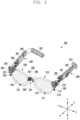
- FIG. 2 is a perspective view schematically illustrating a construction of a wearable electronic device according to various embodiments of the disclosure.
- a wearable electronic device 200 in FIG. 2 may include embodiments described in relation to the electronic device 101 in FIG. 1 .
- the wearable electronic device 200 may include augmented reality (AR) glass having a glasses form or smart glass.
- AR augmented reality
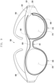
- the wearable electronic device 200 may include a bridge 201, a first rim 210, a second rim 220, a first end piece 230, a second end piece 240, a first temple 250 and/or a second temple 260.
- the bridge 201 may connect the first rim 210 and the second rim 220.
- the bridge 201 may be disposed on the nose of a user when the user wears the wearable electronic device 200.
- the first rim 210 and the second rim 220 may be separated from each other on the basis of the bridge 201.
- the bridge 201 may include a camera module 203, a first eye tracking camera 205, a second eye tracking camera 207 and/or an audio module 209.
- the camera module 203 may photograph a front (e.g., a -y axis direction) of a user (e.g., a user of the wearable electronic device 200), and may obtain image data.
- the camera module 203 may photograph an image corresponding to a field of view (FoV) of a user or may measure a distance from a subject for photographing (e.g., an object).
- the camera module 203 may include an RGB camera, a high resolution (HR) camera and/or a photo video (PV) camera.
- the camera module 203 may include a color camera having an auto focus (AF) function and an optical image stabilization (OIS) function.
- AF auto focus
- OIS optical image stabilization
- the first eye tracking camera 205 and the second eye tracking camera 207 may identify a line of sight watched by a user.
- the first eye tracking camera 205 and the second eye tracking camera 207 may photograph the pupils of a user in a direction opposite to a photographing direction of the camera module 203.
- the first eye tracking camera 205 may partially photograph the left eye of a user
- the second eye tracking camera 207 may partially photograph the right eye of the user.
- the first eye tracking camera 205 and the second eye tracking camera 207 may detect the pupils (e.g., the left eye and the right eye) of a user, and may track a direction of a line of sight.
- the tracked direction of the line of sight may be used for the center of a virtual image, including a virtual object, to move in accordance with a direction of the line of sight.
- the first eye tracking camera 205 and/or the second eye tracking camera 207 may track a line of sight of a user by using at least one method among an electro-oculography or electrooculogram (EOG) sensor, a coil system, a dual Purkinje system, bright pupil systems, or dark pupil systems, for example.
- EOG electro-oculography or electrooculogram
- the audio module 209 (e.g., the audio module 170 in FIG. 1 ) may be disposed between the first eye tracking camera 205 and the second eye tracking camera 207.
- the audio module 209 may convert a voice of a user into an electrical signal or convert an electrical signal into a sound.
- the audio module 209 may include a microphone.
- the first rim 210 and the second rim 220 may form frames (e.g., glasses frames) of the wearable electronic device 200 (e.g., AR glass).
- the first rim 210 may be disposed in a first direction (e.g., an x axis direction) of the bridge 201.
- the first rim 210 may be disposed at a location corresponding to the left eye of the user.
- the second rim 220 may be disposed in a second direction (e.g., an -x axis direction) of the bridge 201, that is, a direction opposite to the first direction (e.g., the x axis direction).
- the second rim 220 may be disposed at a location corresponding to the right eye of the user.
- the first rim 210 and the second rim 220 may be formed by using a metal material and/or a non-metal material (e.g., polymer).
- the first rim 210 may surround and support at least a part of first glass 215 (e.g., a first display) disposed in the inner circumference surface of the first rim 210.
- the first glass 215 may be disposed ahead of the left eye of a user.
- the second rim 220 may surround and support at least a part of second glass 225 (e.g., a second display) disposed in the inner circumference surface of the second rim 220.
- the second glass 225 may be disposed ahead of the right eye of the user.
- a user of the wearable electronic device 200 may watch a foreground (e.g., an actual image) of an outside object (e.g., a subject for photographing) through the first glass 215 and the second glass 225.
- the wearable electronic device 200 may implement AR by overlapping and displaying a virtual image in a foreground (e.g., an actual image) of an outside object.
- the first glass 215 and the second glass 225 may include a projection type transparent display. Each of the first glass 215 and the second glass 225 may form a reflected surface as a transparent plate (or a transparent screen). An image generated by the wearable electronic device 200 may be reflected (e.g., total internal reflection) through the reflected surfaces, and may be incident on the left eye and right eye of a user.
- the first glass 215 may include a waveguide for delivering, to the left eye of a user, light generated by a light source of the wearable electronic device 200.
- the waveguide may be formed by using glass, plastic, or polymer material, and may include a nano pattern (e.g., a grating structure or mesh structure having a polygon or a curved shape) formed within or on a surface of the first glass 215.
- the waveguide may include at least one of at least one diffraction element (e.g., a diffractive optical element (DOE), a holographic optical element (HOE)) or a reflection element (e.g., a reflection mirror).
- DOE diffractive optical element
- HOE holographic optical element
- the waveguide may guide, into an eye of a user, display light emitted from the light source by using at least one diffraction element or a reflection element included in the waveguide.
- the diffraction element may include an input/output optical member.
- the reflection element may include total internal reflection (TIR).
- TIR total internal reflection
- a light path of light emitted from the light source may be guided into the waveguide through the input optical member.
- Light that moves through the waveguide may be guided in an eye direction of a user through the output optical member.
- the second glass 225 may be implemented substantially in the same manner as the first glass 215.
- the first glass 215 and the second glass 225 may include a liquid crystal display (LCD), a digital mirror device (DMD), liquid crystal on silicon (LCoS), an organic light emitting diode (OLED), or a micro light emitting diode (micro LED), for example.
- LCD liquid crystal display
- DMD digital mirror device
- LCDoS liquid crystal on silicon
- OLED organic light emitting diode
- micro LED micro light emitting diode
- the wearable electronic device 200 may include a light source for radiating light to screen output areas of the first glass 215 and the second glass 225.
- the wearable electronic device 200 can provide a user with a virtual image having excellent quality although a separate light source is not included.
- the first rim 210 may include a first microphone 211, a first recognition camera 213, a first light-emitting device 217 and/or a first display module 219.
- the second rim 220 may include a second microphone 221, a second recognition camera 223, a second light-emitting device 227 and/or a second display module 229.
- the first light-emitting device 217 and the first display module 219 may be included in the first end piece 230.
- the second light-emitting device 227 and the second display module 229 may be included in the second end piece 240.
- the first microphone 211 and/or the second microphone 221 may receive a voice of a user of the wearable electronic device 200, and may convert the voice into an electrical signal.
- the first recognition camera 213 and/or the second recognition camera 223 may recognize a surrounding space of the wearable electronic device 200.
- the first recognition camera 213 and/or the second recognition camera 223 may detect a gesture of a user within a given distance (e.g., a given space) of the wearable electronic device 200.
- the first recognition camera 213 and/or the second recognition camera 223 may include a global shutter (GS) camera whose rolling shutter (RS) phenomenon may be reduced in order to detect and track a fast hand movement of a user and/or a fine movement for a finger.
- GS global shutter
- RS rolling shutter
- the wearable electronic device 200 may detect an eye corresponding to a fixing eye and/or a supplementary eye among the left eye and/or right eye of a user by using the first eye tracking camera 205, the second eye tracking camera 207, the first recognition camera 213 and/or the second recognition camera 223.
- the wearable electronic device 200 may detect an eye corresponding to a fixing eye and/or a supplementary eye based on a direction of a line of sight of a user for an outside object or a virtual object.
- the first light-emitting device 217 and/or the second light-emitting device 227 may emit light in order to increase the accuracy of the camera module 203, the first eye tracking camera 205, the second eye tracking camera 207, the first recognition camera 213 and/or the second recognition camera 223.
- the first light-emitting device 217 and/or the second light-emitting device 227 may be used as assistant means for increasing accuracy when a pupil of a user is photographed by using the first eye tracking camera 205 and/or the second eye tracking camera 207.
- the first light-emitting device 217 and/or the second light-emitting device 227 may be used as assistant means when it is not easy to detect an object (e.g., a subject for photographing) to be photographed due to a dark environment or the mixing of several light sources and reflected light if a gesture of a user is photographed by using the first recognition camera 213 and/or the second recognition camera 223.
- the first light-emitting device 217 and/or the second light-emitting device 227 may include an LED, an IR LED, or a xenon lamp, for example.
- the first display module 219 and/or the second display module 229 may emit light, and may transmit the light to the left eye and/or right eye of a user by using the first glass 215 and/or the second glass 225.
- the first glass 215 and/or the second glass 225 may display various types of image information by using the light emitted through the first display module 219 and/or the second display module 229.
- the first display module 219 and/or the second display module 229 may include the display module 160 in FIG. 1 .
- the wearable electronic device 200 may overlap and display, through the first glass 215 and/or the second glass 225, a foreground of an outside object and an image discharged through the first display module 219 and/or the second display module 229.
- the first end piece 230 may be combined with a part (e.g., the x axis direction) of the first rim 210.
- the second end piece 240 may be combined with a part (e.g., the -x axis direction) of the second rim 220.
- the first light-emitting device 217 and the first display module 219 may be included in the first end piece 230.
- the second light-emitting device 227 and the second display module 229 may be included in the second end piece 240.
- the first end piece 230 may connect the first rim 210 and the first temple 250.
- the second end piece 240 may connect the second rim 220 and the second temple 260.
- the first temple 250 may be operatively connected to the first end piece 230 by using a first hinge part 255.
- the first hinge part 255 may be rotatably constructed so that the first temple 250 is folded or unfolded with respect to the first rim 210.
- the first temple 250 may extend along the left side of the head of a user, for example.
- a tail part (e.g., a y axis direction) of the first temple 250 may be constructed in a bent form when a user wears the wearable electronic device 200, for example, so that the tail part is supported by the left ear of the user.
- the second temple 260 may be operatively connected to the second end piece 240 by using a second hinge part 265.
- the second hinge part 265 may be rotatably constructed so that the second temple 260 is folded or unfolded with respect to the second rim 220.
- the second temple 260 may extend along the right side of the head of a user, for example.
- a tail part (e.g., the y axis direction) of the second temple 260 may be constructed in a bent form when a user wears the wearable electronic device 200, for example, so that the tail part is supported by the right ear of the user.
- the first temple 250 may include a first printed circuit substrate 251, a first sound output module 253 (e.g., the sound output module 155 in FIG. 1 ) and/or a first battery 257 (e.g., the battery 189 in FIG. 1 ).
- the second temple 260 may include a second printed circuit substrate 261, a second sound output module 263 (e.g., the sound output module 155 in FIG. 1 ) and/or a second battery 267 (e.g., the battery 189 in FIG. 1 ).
- various electronic parts may be mounted on the first printed circuit substrate 251 and/or the second printed circuit substrate 261.
- the processor may include one or more of a central processing unit, an application processor, a graphic processor, an image signal processor, a sensor hub processor, or a communication processor, for example.
- the first printed circuit substrate 251 and/or the second printed circuit substrate 261 may include a printed circuit board (PCB), a flexible PCB (FPCB), or a rigid-flexible PCB (RFPCB), for example.
- PCB printed circuit board
- FPCB flexible PCB
- RFPCB rigid-flexible PCB
- the first printed circuit substrate 251 and/or the second printed circuit substrate 261 may include a main PCB, a slave PCB partially overlapped with the main PCB and disposed therein and/or an interposer substrate between the main PCB and the slave PCB.
- the first printed circuit substrate 251 and/or the second printed circuit substrate 261 may be electrically connected to other components (e.g., the camera module 203, the first eye tracking camera 205, the second eye tracking camera 207, the audio module 209, the first microphone 211, the first recognition camera 213, the first light-emitting device 217, the first display module 219, the second microphone 221, the second recognition camera 223, the second light-emitting device 227, the second display module 229, the first sound output module 253 and/or the second sound output module 263) by using an electrical path, such as an FPCB and/or a cable.
- other components e.g., the camera module 203, the first eye tracking camera 205, the second eye tracking camera 207, the audio module 209, the first microphone 211, the first recognition camera 213, the first light-emitting device 217, the first display module 219, the second microphone 221, the second recognition camera 223, the second light-emitting device 227, the second display module 229, the first sound
- the FPCB and/or the cable may be disposed in at least some of the first rim 210, the bridge 201 and/or the second rim 220.
- the wearable electronic device 200 may include only one of the first printed circuit substrate 251 or the second printed circuit substrate 261.
- the first sound output module 253 and/or the second sound output module 263 may deliver an audio signal to the left and/or right ears of a user.
- the first sound output module 253 and/or the second sound output module 263 may include a pizeo speaker (e.g., a bone conduction speaker) for delivering an audio signal without a speaker hole, for example.
- the wearable electronic device 200 may include only one of the first sound output module 253 or the second sound output module 263.
- the first battery 257 and/or the second battery 267 may supply power to the first printed circuit substrate 251 and/or the second printed circuit substrate 261 by using a power management module (e.g., the power management module 188 in FIG. 1 ).
- the first battery 257 and/or the second battery 267 may include a primary cell incapable of being recharged, a secondary cell capable of being recharged, or a fuel cell, for example.
- the wearable electronic device 200 may include only one of the first battery 257 or the second battery 267.
- the wearable electronic device 200 may include a sensor module (e.g., the sensor module 176 in FIG. 1 ).
- the sensor module may generate an electrical signal or data value that corresponds to an operating state within the wearable electronic device 200 or an external environment state.
- the sensor module may further include at least one of a gesture sensor, a gyro sensor, an atmospheric sensor, a magnetic sensor, an acceleration sensor, a grip sensor, a color sensor, an infrared (IR) sensor, a bio sensor (e.g., an HRM sensor), a temperature sensor, a humidity sensor, or an illuminance sensor, for example.
- a gesture sensor e.g., the sensor module 176 in FIG. 1
- the sensor module may generate an electrical signal or data value that corresponds to an operating state within the wearable electronic device 200 or an external environment state.
- the sensor module may further include at least one of a gesture sensor, a gyro sensor, an atmospheric sensor, a magnetic sensor, an acceleration sensor, a grip sensor
- the sensor module may recognize bio information of a user by using various bio sensors (or a bio recognition sensor), such as an e-nose sensor, an electromyography (EMG) sensor, an electroencephalogram (EEG) sensor, an electrocardiogram (ECG) sensor, or an iris sensor.
- bio sensors or a bio recognition sensor
- EMG electromyography
- EEG electroencephalogram
- ECG electrocardiogram
- iris sensor an iris sensor
- the wearable electronic device 200 is a device which displays AR by using the first glass 215 and the second glass 225, but the disclosure is not limited thereto.
- the wearable electronic device 200 may be a device which displays virtual reality (VR).
- VR virtual reality
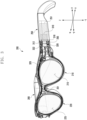
- FIG. 3 is a perspective view schematically illustrating a wearable electronic device including an antenna according to various embodiments of the disclosure.
- a wearable electronic device 200 in FIG. 3 may include embodiments described in relation to the wearable electronic device 200 in FIG. 2 .
- the wearable electronic device 200 disclosed in FIG. 3 may be a drawing illustrating only some components of the wearable electronic device 200 disclosed in FIG. 2 .
- the wearable electronic device 200 disclosed in FIG. 3 may be integrated with or applied to the wearable electronic device 200 in FIG. 2 .
- substantially the same components as those of the embodiment of the wearable electronic device 200 in FIG. 2 may be assigned the same reference numerals, and a redundant description thereof may be omitted.
- the wearable electronic device 200 may include a bridge 201, a first rim 210, a second rim 220, a first temple 250, a second temple 260 and/or a conductive pattern 320.
- the bridge 201 may connect the first rim 210 and the second rim 220.
- the bridge 201 may be formed by using a non-metal material (e.g., polymer).
- the first rim 210 and the second rim 220 may form a frame (e.g., a glasses frame) of the wearable electronic device 200.
- the first rim 210 and the second rim 220 may be formed by using a non-metal material (e.g., a non-conductive injection).
- the first rim 210 may be disposed in a first direction (e.g., an x axis direction) of the bridge 201.
- the first rim 210 may be disposed around the left eye of a user.
- the second rim 220 may be disposed in a second direction (e.g., an -x axis direction) of the bridge 201, that is, a direction opposite to the first direction (e.g., the x axis direction).
- the second rim 220 may be disposed around the right eye of the user.
- the first rim 210 may surround and support at least a part of first glass 215 (e.g., a first display) disposed in an inner circumference surface of the first rim 210.
- the first glass 215 may be disposed ahead of the left eye of a user.
- the second rim 220 may surround and support at least a part of second glass 225 (e.g., a second display) disposed in an inner circumference surface of the second rim 220.
- the second glass 225 may be disposed ahead of the right eye of the user.
- the first temple 250 may be operatively connected to at least a part of the first rim 210 by using a first hinge part 255.
- the first hinge part 255 may be rotatably constructed so that the first temple 250 is folded or unfolded with respect to the first rim 210.
- the first hinge part 255 may be formed by using a conductive material (e.g., metal).
- the first temple 250 may extend along the left side of the head of a user, for example.
- the second temple 260 may be operatively connected to at least a part of the second rim 220 by using a second hinge part (e.g., the second hinge part 265 in FIG. 2 ).
- the second hinge part 265 may be rotatably constructed so that the second temple 260 is folded or unfolded with respect to the second rim 220.
- the second hinge part 265 may be formed by using a conductive material (e.g., metal).
- the second temple 260 may extend along the right side of the head of the user, for example.
- the first temple 250 may include a first printed circuit substrate 251.
- the second temple 260 may include a second printed circuit substrate (e.g., the second printed circuit substrate 261 in FIG. 2 .
- constructions and functions of the first printed circuit substrate 251 and the second printed circuit substrate 261 are substantially the same, and only the construction and function of the first printed circuit substrate 251 may be described.
- the first printed circuit substrate 251 may include a wireless communication module 310 (e.g., the wireless communication module 192 in FIG. 1 ).
- the first printed circuit substrate 251 may include a feed part 312 and a ground 316 electrically connected to the wireless communication module 310.
- the conductive pattern 320 may be disposed in at least a part of an inner circumference surface of the first rim 210, the bridge 201, and at least a part of an inner circumference surface of the second rim 210.
- the conductive pattern 320 may be disposed in at least a part of an outer circumference surface of the first glass 215, the bridge 201, and at least a part of an outer circumference surface of the second glass 225.
- the antenna may be formed of a strip (e.g., as seen in FIG. 3 , as indicated by the conductive pattern reference number 320), of an appropriate material for an antenna (e.g., metal) on which the conductive pattern 320 may be formed so as to enhance radiative properties of the antenna.
- the conductive pattern 320 may be disposed between at least a part of the inner circumference surface of the first rim 210 and at least a part of the outer circumference surface of the first glass 215 and within the bridge 201.
- the conductive pattern 320 may be disposed between at least a part of the inner circumference surface of the second rim 220 and at least a part of the outer circumference surface of the second glass 225.
- the conductive pattern 320 may include a conductive sheet or a conductive film.
- a first part 322 of the conductive pattern 320 may be electrically connected to the feed part 312 of the first printed circuit substrate 251, and a second part 326 thereof may be electrically connected to the ground 316 of the first printed circuit substrate 251.
- the conductive pattern 320 may pass through the inside of the bridge 201 after passing between at least a part of the inner circumference surface of the first rim 210 and at least a part of the outer circumference surface of the first glass 215 in the state in which the first part 322 has been electrically connected to the feed part 312, may pass through the inside of the bridge 201 after passing between at least a part of the inner circumference surface of the second rim 220 and at least a part of the outer circumference surface of the second glass 225, and may extend to pass between at least a part of the inner circumference surface of the first rim 210 and at least a part of the outer circumference surface of the first glass 215.
- the second part 326 of the conductive pattern 320 may be electrically connected to the ground 316.
- a loop antenna may be formed.
- the first hinge part 255 may be electrically connected to the wireless communication module 310 of the first printed circuit substrate 251, and may perform the function of the feed part 312.
- a conductive connection member e.g., a screw
- a conductive connection member e.g., a screw
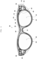
- FIG. 4 is a diagram schematically illustrating a wearable electronic device including a plurality of antennas according to various embodiments of the disclosure.
- FIG. 4 may be a drawing of the wearable electronic device 200 disclosed in FIG. 3 according to various embodiments of the disclosure, which is viewed in one direction (e.g., a - y axis direction).
- a wearable electronic device 200 in FIG. 4 may include embodiments described in the wearable electronic device 200 in FIGS. 2 and/or 3.
- the wearable electronic device 200 disclosed in FIG. 4 may be a drawing illustrating only some components of the wearable electronic device 200 disclosed in FIG. 2 .
- the wearable electronic device 200 disclosed in FIG. 4 may be integrated with or applied to the wearable electronic device 200 in FIGS. 2 and/or 3.
- substantially the same components as those of the embodiments of the wearable electronic device 200 in FIGS. 2 and/or 3 may be assigned the same reference numerals, and a redundant description thereof may be omitted.
- the wearable electronic device 200 may include a bridge 201, a first rim 210, a second rim 220, a first temple 250, a second temple 260, a flexible printed circuit board (FPCB) 420, a conductive pattern 320 and/or a conductive stub 430.
- FPCB flexible printed circuit board
- the conductive pattern 320 may operate as a first antenna (e.g., a first antenna radiator).
- the conductive stub 430 may operate as a second antenna (e.g., a second antenna radiator).
- the bridge 201 may connect the first rim 210 and the second rim 220.
- the bridge 201 may be formed by using a non-metal material (e.g., polymer).
- the first rim 210 and the second rim 220 may form a frame (e.g., a glasses frame) of the wearable electronic device 200.
- the first rim 210 and the second rim 220 may be formed by using a non-metal material (e.g., a non-conductive injection).
- the first rim 210 may be disposed in a first direction (e.g., the x axis direction) of the bridge 201.
- the first rim 210 may be disposed around the left eye of a user.
- the second rim 220 may be disposed in a second direction (e.g., the -x axis direction) of the bridge 201, that is, a direction opposite to the first direction (e.g., the x axis direction).
- the second rim 220 may be disposed around the right eye of the user.
- the first rim 210 may surround and support at least a part of first glass 215 (e.g., a first display) disposed in an inner circumference surface of the first rim 210.
- the first glass 215 may be disposed ahead of the left eye of a user.
- the second rim 220 may surround and support at least a part of second glass 225 (e.g., a second display) disposed in an inner circumference surface of the second rim 220.
- the second glass 225 may be disposed ahead of the right eye of a user.
- the first temple 250 may be operatively connected to at least a part of the first rim 210 by using a first hinge part (e.g., the first hinge part 255 in FIG. 3 ).
- the first temple 250 may extend along the left side of the head of a user, for example.
- the second temple 260 may be operatively connected to at least a part of the second rim 220 by using a second hinge part (e.g., the second hinge part 265 in FIG. 2 ).
- the second temple 260 may extend along the right side of the head of a user, for example.
- the first temple 250 may include a first printed circuit substrate 251.
- the second temple 260 may include a second printed circuit substrate (e.g., the second printed circuit substrate 261 in FIG. 2 ).
- the first printed circuit substrate 251 and/or the second printed circuit substrate 261 may include a wireless communication module (e.g., the wireless communication module 310 in FIG. 3 ).
- constructions and functions of the first printed circuit substrate 251 and the second printed circuit substrate 261 are substantially the same, and only the construction and function of the first printed circuit substrate 251 may be described.
- the FPCB 420 may be disposed on the inside of the top (e.g., a z axis direction) of the first rim 210 and the second rim 220.
- the FPCB 420 may be disposed to intersect the top of the first glass 215, the bridge 201, and the second glass 225.
- the FPCB 420 may be electrically connected to the first printed circuit substrate 251 by using a conductive connection member 425 (e.g., a solder, a conductive connector, or a conductive foam spring).
- the FPCB 420 may have a feed part 401 formed at a portion adjacent to the first printed circuit substrate 251 and have a ground 405 formed at a portion adjacent to the bridge 201.
- the feed part 401 and the ground 405 may be formed at portions adjacent to the first rim 210. In another embodiment, locations of the feed part 401 and ground 405 of the FPCB 420 are not limited to the aforementioned examples, and the feed part 401 and ground 405 may be formed at various locations.
- the conductive pattern 320 may be disposed in at least a part of an inner circumference surface of the first rim 210, the bridge 201 and at least a part of an inner circumference surface of the second rim 210.
- the conductive pattern 320 may be disposed in at least a part of an outer circumference surface of the first glass 215, the bridge 201, and at least a part of the outer circumference surface of the second glass 225.
- the conductive pattern 320 may be disposed between at least a part of the inner circumference surface of the first rim 210 and at least a part of the outer circumference surface of the first glass 215 and within the bridge 201.
- the conductive pattern 320 may be disposed between at least a part of the inner circumference surface of the second rim 220 and at least a part of the outer circumference surface of the second glass 225.
- the conductive pattern 320 may include a conductive sheet or a conductive film.
- the first part 322 of the conductive pattern 320 may be electrically connected to the feed part 401 of the FPCB 420, and the second part 326 thereof may be electrically connected to the ground 405 of the FPCB 420.
- the conductive pattern 320 may pass through the inside of the bridge 201 after passing between at least a part of the inner circumference surface of the first rim 210 and at least a part of the outer circumference surface of the first glass 215 in the state in which the first part 322 has been electrically connected to the feed part 401, may pass through the inside of the bridge 201 after passing between at least a part of the inner circumference surface of the second rim 220 and at least a part of the outer circumference surface of the second glass 225, and may extend to at least a part of the inner circumference surface of the first rim 210 and at least a part of the outer circumference surface of the first glass 215.
- the second part 326 may be electrically connected to the ground 405 of the FPCB 420.
- the conductive stub 430 may have a first part 431 electrically connected to the feed part 401 of the FPCB 420, and may have a second part 432 extended in a designated length.
- the conductive stub 430 may be used for the adjustment of a resonant length (e.g., a resonant frequency), a change in the radiation pattern and/or impedance matching.
- the conductive stub 430 may be formed within the first glass 215.
- the feed part 401 may be electrically connected to the first part 322 of the conductive pattern 320 and the first part 431 of the conductive stub 430.
- the feed part 401 may be electrically connected to the first part 322 of the conductive pattern 320 and the first part 431 of the conductive stub 430 by using a conductive connection member (e.g., a C-clip or a conductive foam spring).
- the first part 322 of the conductive pattern 320 and the first part 431 of the conductive stub 430 may use the feed part 401 of the FPCB 420 in common.
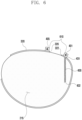
- FIG. 5 is a diagram illustrating a form in which a conductive pattern of a wearable electronic device according to various embodiments of the disclosure surrounds a part of first glass.
- FIG. 6 is a diagram illustrating an embodiment in which a conductive pattern of a wearable electronic device according to various embodiments of the disclosure surrounds a part of the first glass and includes a conductive connection member.
- FIGS. 5 and 6 may illustrate embodiments in which a part of the conductive pattern 320 surrounds the first glass 215 of the wearable electronic device 200 according to various embodiments of the disclosure.
- At least a part of the conductive pattern 320 of the wearable electronic device 200 may surround the outer circumference surface (e.g., a border) of the first glass 215.
- the conductive pattern 320 may have the first part 322 electrically connected to the feed part 401 of an FPCB (e.g., the FPCB 420 in FIG. 4 ) and the second part 326 electrically connected to the ground 405 of the FPCB 420.
- an FPCB e.g., the FPCB 420 in FIG. 4
- the second part 326 electrically connected to the ground 405 of the FPCB 420.
- the conductive stub 430 may have the first part 431 electrically connected to the feed part 401 of the FPCB 420 and have the second part 432 extended in a designated length.
- the conductive stub 430 may include a mesh pattern or a lattice pattern.
- the first part 322 of the conductive pattern 320 and the first part 431 of the conductive stub 430 may be electrically connected to the feed part 401.
- the first part 322 of the conductive pattern 320 and the first part 431 of the conductive stub 430 may use the feed part 401 of the FPCB 420 in common use.
- the feed part 401 of the FPCB 420 may be electrically connected to the first part 322 of the conductive pattern 320 and the first part 431 of the conductive stub 430 by using a conductive connection member 610.
- the ground 405 of the FPCB 420 may be electrically connected to the second part 326 of the conductive pattern 320 by using the conductive connection member 610.
- the conductive connection member 610 may include a pad for contact, a coupling member, a C-clip, or a conductive foam spring, for example.
- FIG. 7 is a diagram schematically illustrating a construction of the first glass of the wearable electronic device according to various embodiments of the disclosure.
- FIG. 7 describes the first glass 215 of the wearable electronic device 200 according to various embodiments of the disclosure, but the second glass 225 may also be constructed substantially in the same manner as the first glass 215.
- the conductive pattern 320 and/or the conductive stub 430 may be formed within the first glass 215 (or the second glass 225).
- the first glass 215 may include a first layer 710, a second layer 720 and/or a third layer 730.
- the first layer 710 may include a window (e.g., a transparent protection layer).
- the second layer 720 may include a display panel.
- the third layer 730 may include a non-conductive support member.
- the conductive pattern 320 may be formed in an outer circumference surface (e.g., an edge or a border) of the second layer 720 (e.g., the display panel) disposed between the first layer 710 (e.g., a window) and the third layer 730 (e.g., a non-conductive support member).
- the conductive stub 430 may also be disposed on a surface of the second layer 720 in a designated length.
- FIG. 8 is a diagram illustrating an embodiment of a conductive pattern of a wearable electronic device according to various embodiments of the disclosure.
- parts of the conductive pattern 320 of the wearable electronic device 200 may be intersected at the bridge 201. If parts of the conductive pattern 320 are disposed to be intersected at the bridge 201, an isotropic radiation pattern may be implemented.
- the first part 322 of the conductive pattern 320 may pass through the bridge 201 along the inner circumference surface of the first rim 210 or the outer circumference surface of the first glass 215, and may extend along the inner circumference surface of the second rim 220 or the outer circumference surface of the second glass 225 and cross each other at the bridge 201.
- the second part 326 of the conductive pattern 320 may be disposed in a part of the first rim 210.
- the first part 322 of the conductive pattern 320 may be electrically connected to the feed part 312 or 401, and the second part 326 thereof may be electrically connected to the ground 316 or 405.
- FIG. 9 is a diagram illustrating an embodiment of a conductive stub of a wearable electronic device according to various embodiments of the disclosure.
- the conductive stub 430 of the wearable electronic device 200 may form a loop in the first rim 210. If the conductive stub 430 forms a dual loop along with the conductive pattern 320 in the first rim 210, an additional resonant length can be secured.
- the first part 322 of the conductive pattern 320 may pass through the bridge 201 along the inner circumference surface of the first rim 210 or the outer circumference surface of the first glass 215, and may extend along the inner circumference surface of the second rim 220 or the outer circumference surface of the second glass 225 and pass through the bridge 201.
- the second part 326 of the conductive pattern 320 may be disposed in a part of the first rim 210.
- the first part 322 of the conductive pattern 320 may be electrically connected to the feed part 312 or 401, and the second part 326 may be electrically connected to the ground 316 or 405.
- the first part 431 of the conductive stub 430 may be electrically connected to the feed part 312 or 401 along with the first part 322 of the conductive pattern 320.
- the conductive stub 430 may extend along a lower border of the first rim 210 from the first part 322.
- the second part 432 may be electrically connected to a part of the conductive pattern 320.
- the conductive stub 430 may form a dual loop along with at least a part of the conductive pattern 320 in the first rim 210.
- FIG. 10 is a diagram illustrating radiation performance of a wearable electronic device according to various embodiments of the disclosure and a wearable electronic device according to a comparison embodiment.
- the conductive pattern 320 of an electronic device may be disposed in at least a part of the first rim 210, the bridge 201, and the second rim 220, and may operate as a loop antenna.
- the wearable electronic device 200 may have the conductive stub 430 additionally disposed therein.
- a conductive pattern of the wearable electronic device according to the comparison embodiment may be disposed only in a part of the first rim 210 or the second rim 220.
- radiation efficiency of the wearable electronic device 200 may appear like P2 (e.g., a solid line in FIG. 10 ), and radiation efficiency of the wearable electronic device according to the comparison embodiment may appear like P1 (e.g., a dotted line in FIG. 10 ).
- the wearable electronic device 200 has become better radiation efficiency P2 in about 0.7 GHz to 0.9 GHz band and about 1.7 GHz to 3.2 GHz band compared to radiation efficiency P1 of the wearable electronic device according to the comparison embodiment.
- the wearable electronic device 200 may include the bridge 201, the first rim 210 disposed in a first direction of the bridge and the second rim 220 disposed in a second direction of the bridge which is a direction opposite to the first direction, the first glass 215 disposed to have at least a part thereof surrounded by the first rim and the second glass 225 disposed to have at least a part thereof surrounded by the second rim, the first temple 250 operatively connected to at least a part of the first rim by using the first hinge part 255 and the second temple 260 operatively connected to at least a part of the second rim by using the second hinge part 265, the first printed circuit substrate 251 disposed within the first temple and including the wireless communication module 310, the FPCB 420 electrically connected to the first printed circuit substrate, disposed in at least a part of the first rim, the bridge, and the second rim, and including the feed part 401 and the ground 405, the conductive pattern 320 disposed in at least a part of
- the conductive pattern may have the first part 322 electrically connected to the feed part and extended through the first rim, the bridge, the second rim, and the first rim and have the second part 326 electrically connected to the ground.
- the conductive stub may be constructed to have the first part 431 electrically connected to the feed part.
- the conductive pattern 320 may be constituted to operate as a first antenna, and the conductive stub 430 may be constituted to operate as a second antenna.
- the first rim, the bridge, and the second rim may be formed by using a non-conductive material.
- the first printed circuit substrate may be electrically connected to the FPCB by using the conductive connection member 425.
- the conductive pattern may be disposed in at least a part of an outer circumference surface of the first glass, the bridge, and an outer circumference surface of the second glass.
- the second part 432 of the conductive stub may extend in a designated length.
- the conductive stub may include a mesh pattern or a lattice pattern.
- the feed part and/or the ground may be electrically connected to the conductive pattern by using the conductive connection member 610.
- the conductive connection member 610 may include a pad for contact, a coupling member, a C-clip, or a conductive foam spring.
- the first glass may include the first layer 710, the second layer 720, and the third layer 730, and the conductive pattern may be disposed in the outer circumference surface of the second layer.
- the conductive stub may be disposed in the second layer 720.
- the conductive pattern may be disposed to be intersected at the bridge.
- the second part 432 of the conductive stub may extend along at least a part of a border of the first rim, and may be electrically connected to a part of the conductive pattern.
- the feed part may be disposed at a portion adjacent to the first printed circuit substrate, and the ground may be disposed at a portion adjacent to the bridge.
- the wearable electronic device 200 may include the bridge 201, the first rim 210 disposed in a first direction of the bridge and the second rim 220 disposed in a second direction of the bridge which is a direction opposite to the first direction, the first glass 215 disposed to have at least a part thereof surrounded by the first rim and the second glass 225 disposed to have at least a part thereof surrounded by the second rim, the first temple 250 operatively connected to at least a part of the first rim by using the first hinge part 255 and the second temple 260 operatively connected to at least a part of the second rim by using the second hinge part 265, the first printed circuit substrate 251 disposed within the first temple and including the ground 316, the wireless communication module 310 disposed in the first printed circuit substrate and including the feed part 312, and the conductive pattern 320 disposed in at least a part of the first rim, the bridge, and the second rim.
- the conductive pattern may have the first part 322 electrically connected to the feed
Landscapes
- Physics & Mathematics (AREA)
- Health & Medical Sciences (AREA)
- Acoustics & Sound (AREA)
- General Health & Medical Sciences (AREA)
- Otolaryngology (AREA)
- General Physics & Mathematics (AREA)
- Ophthalmology & Optometry (AREA)
- Optics & Photonics (AREA)
- Engineering & Computer Science (AREA)
- Microelectronics & Electronic Packaging (AREA)
- Eyeglasses (AREA)
Applications Claiming Priority (2)
| Application Number | Priority Date | Filing Date | Title |
|---|---|---|---|
| KR1020210138363A KR20230055091A (ko) | 2021-10-18 | 2021-10-18 | 안테나를 포함하는 웨어러블 전자 장치 |
| PCT/KR2022/014628 WO2023068588A1 (ko) | 2021-10-18 | 2022-09-29 | 안테나를 포함하는 웨어러블 전자 장치 |
Publications (2)
| Publication Number | Publication Date |
|---|---|
| EP4386979A1 true EP4386979A1 (de) | 2024-06-19 |
| EP4386979A4 EP4386979A4 (de) | 2025-01-08 |
Family
ID=85982236
Family Applications (1)
| Application Number | Title | Priority Date | Filing Date |
|---|---|---|---|
| EP22883812.4A Pending EP4386979A4 (de) | 2021-10-18 | 2022-09-29 | Tragbare elektronische vorrichtung mit antenne |
Country Status (3)
| Country | Link |
|---|---|
| US (2) | US12230869B2 (de) |
| EP (1) | EP4386979A4 (de) |
| CN (1) | CN118104070A (de) |
Families Citing this family (3)
| Publication number | Priority date | Publication date | Assignee | Title |
|---|---|---|---|---|
| US12334629B2 (en) * | 2022-01-12 | 2025-06-17 | Samsung Electronics Co., Ltd. | Wearable electronic device including antenna |
| US12469953B2 (en) * | 2022-05-06 | 2025-11-11 | Meta Platforms Technologies, Llc | Antenna for wearable electronic devices |
| US12501175B2 (en) * | 2022-07-07 | 2025-12-16 | Pupil Labs Gmbh | Camera module, head-wearable eye tracking device, and method for manufacturing a camera module |
Family Cites Families (16)
| Publication number | Priority date | Publication date | Assignee | Title |
|---|---|---|---|---|
| JP2003202525A (ja) * | 2002-01-09 | 2003-07-18 | Sun-Lux Optical Co Ltd | レンズ、玉型、及び眼鏡 |
| US8465151B2 (en) * | 2003-04-15 | 2013-06-18 | Ipventure, Inc. | Eyewear with multi-part temple for supporting one or more electrical components |
| US9285592B2 (en) | 2011-08-18 | 2016-03-15 | Google Inc. | Wearable device with input and output structures |
| JP5944134B2 (ja) * | 2011-10-14 | 2016-07-05 | シャープ株式会社 | 無線通信機 |
| KR102230167B1 (ko) | 2014-12-11 | 2021-03-19 | 서울과학기술대학교 산학협력단 | 안경부착형 투명 안테나 모듈 및 이를 통한 sar 저감형성방법 |
| KR20160080444A (ko) * | 2014-12-29 | 2016-07-08 | 삼성전자주식회사 | 안테나 장치 및 그를 구비하는 전자 장치 |
| US20160204839A1 (en) * | 2015-01-12 | 2016-07-14 | Futurewei Technologies, Inc. | Multi-band Antenna for Wearable Glasses |
| JP2017175435A (ja) | 2016-03-24 | 2017-09-28 | 京セラ株式会社 | 電子機器 |
| KR20190120349A (ko) * | 2017-03-06 | 2019-10-23 | 스냅 인코포레이티드 | 웨어러블 디바이스 안테나 시스템 |
| US10534203B2 (en) | 2017-07-31 | 2020-01-14 | Snap Inc. | Near-field antenna for eyewear |
| EP4411462A3 (de) | 2018-01-24 | 2024-10-23 | Snap Inc. | Hybridantennensystem für wearable-vorrichtungen |
| CN209448018U (zh) * | 2019-04-15 | 2019-09-27 | 潍坊歌尔电子有限公司 | 一种智能眼镜的天线结构及智能眼镜 |
| US11372251B2 (en) * | 2019-06-17 | 2022-06-28 | Google Llc | Systems, devices, and methods for electrical pathways between components in wearable heads-up displays |
| US11333905B2 (en) * | 2019-11-14 | 2022-05-17 | Meta Platforms, Inc. | Hinge feed antenna of eyewear |
| CN211263977U (zh) | 2020-01-10 | 2020-08-14 | 芋头科技(杭州)有限公司 | 镜腿弯折结构和包括其的智能眼镜 |
| US11929548B2 (en) * | 2021-07-28 | 2024-03-12 | Snap Inc. | Eyewear with slot-ring antenna |
-
2022
- 2022-09-29 CN CN202280069910.8A patent/CN118104070A/zh active Pending
- 2022-09-29 EP EP22883812.4A patent/EP4386979A4/de active Pending
- 2022-10-27 US US17/974,982 patent/US12230869B2/en active Active
-
2025
- 2025-02-05 US US19/045,715 patent/US20250192421A1/en active Pending
Also Published As
| Publication number | Publication date |
|---|---|
| EP4386979A4 (de) | 2025-01-08 |
| CN118104070A (zh) | 2024-05-28 |
| US20230121025A1 (en) | 2023-04-20 |
| US12230869B2 (en) | 2025-02-18 |
| US20250192421A1 (en) | 2025-06-12 |
Similar Documents
| Publication | Publication Date | Title |
|---|---|---|
| EP4362612B1 (de) | Brillenartige elektronische vorrichtung mit flexibler leiterplatte | |
| US20250192421A1 (en) | Wearable electronic device including antenna | |
| EP4492206A1 (de) | Tragbare elektronische vorrichtung zur anzeige eines virtuellen objekts und steuerungsverfahren dafür | |
| US12487475B2 (en) | Wearable electronic device including antenna | |
| EP4382988A1 (de) | Elektronische vorrichtung mit antennenstruktur | |
| US12334629B2 (en) | Wearable electronic device including antenna | |
| US12276800B2 (en) | Wearable device for adjusting light transmittance according to illuminance of external light source, and method for controlling same | |
| US20220179215A1 (en) | Wearable electronic device including light emitting unit | |
| KR20230037944A (ko) | 플렉서블 회로 기판을 포함하는 안경형 전자 장치 | |
| US20230204985A1 (en) | Wearable electronic device | |
| KR20230055091A (ko) | 안테나를 포함하는 웨어러블 전자 장치 | |
| US12498577B2 (en) | Wearable electronic device including display module | |
| US12306680B2 (en) | Electronic device including connection member | |
| EP4503011A1 (de) | Tragbare vorrichtung zur anpassung der grösse eines effektiven anzeigebereichs gemäss externer beleuchtung und steuerungsverfahren dafür | |
| US11762486B2 (en) | Electronic device for performing plurality of functions using stylus pen and method for operating same | |
| EP4198682A1 (de) | Elektronische vorrichtung mit lautsprecher | |
| US20250138328A1 (en) | Wearable electronic device comprising heat transfer member | |
| EP4369155B1 (de) | Tragbare elektronische vorrichtung und verfahren zur identifizierung einer steuerung unter verwendung einer tragbaren elektronischen vorrichtung | |
| US20250164807A1 (en) | Wearable electronic device comprising lens barrel | |
| EP4629046A1 (de) | Tragbare vorrichtung zur steuerung mindestens eines virtuellen objekts gemäss attributen mindestens eines virtuellen objekts und verfahren zur steuerung davon | |
| US20250237889A1 (en) | Wearable electronic device comprising plurality of hinge structures | |
| US20240356204A1 (en) | Wearable electronic device comprising antenna | |
| KR20230067384A (ko) | 안테나를 포함하는 웨어러블 전자 장치 | |
| KR20240011587A (ko) | 렌즈리스 카메라를 포함하는 웨어러블 전자 장치 및 이를 이용한 이미지 처리 방법 | |
| KR20240141605A (ko) | 페이스 커버 |
Legal Events
| Date | Code | Title | Description |
|---|---|---|---|
| STAA | Information on the status of an ep patent application or granted ep patent |
Free format text: STATUS: THE INTERNATIONAL PUBLICATION HAS BEEN MADE |
|
| PUAI | Public reference made under article 153(3) epc to a published international application that has entered the european phase |
Free format text: ORIGINAL CODE: 0009012 |
|
| STAA | Information on the status of an ep patent application or granted ep patent |
Free format text: STATUS: REQUEST FOR EXAMINATION WAS MADE |
|
| 17P | Request for examination filed |
Effective date: 20240314 |
|
| AK | Designated contracting states |
Kind code of ref document: A1 Designated state(s): AL AT BE BG CH CY CZ DE DK EE ES FI FR GB GR HR HU IE IS IT LI LT LU LV MC MK MT NL NO PL PT RO RS SE SI SK SM TR |
|
| A4 | Supplementary search report drawn up and despatched |
Effective date: 20241204 |
|
| RIC1 | Information provided on ipc code assigned before grant |
Ipc: G02C 11/00 20060101ALI20241129BHEP Ipc: H01Q 21/30 20060101ALI20241129BHEP Ipc: H01Q 7/00 20060101ALI20241129BHEP Ipc: H01Q 1/27 20060101AFI20241129BHEP |
|
| DAV | Request for validation of the european patent (deleted) | ||
| DAX | Request for extension of the european patent (deleted) |