EP4380335A1 - Method of manufacturing a perovskite photovoltaic cell - Google Patents
Method of manufacturing a perovskite photovoltaic cell Download PDFInfo
- Publication number
- EP4380335A1 EP4380335A1 EP22210577.7A EP22210577A EP4380335A1 EP 4380335 A1 EP4380335 A1 EP 4380335A1 EP 22210577 A EP22210577 A EP 22210577A EP 4380335 A1 EP4380335 A1 EP 4380335A1
- Authority
- EP
- European Patent Office
- Prior art keywords
- perovskite
- layer
- providing
- charge transport
- transport layer
- Prior art date
- Legal status (The legal status is an assumption and is not a legal conclusion. Google has not performed a legal analysis and makes no representation as to the accuracy of the status listed.)
- Pending
Links
Images




Classifications
-
- H—ELECTRICITY
- H10—SEMICONDUCTOR DEVICES; ELECTRIC SOLID-STATE DEVICES NOT OTHERWISE PROVIDED FOR
- H10K—ORGANIC ELECTRIC SOLID-STATE DEVICES
- H10K71/00—Manufacture or treatment specially adapted for the organic devices covered by this subclass
- H10K71/10—Deposition of organic active material
- H10K71/12—Deposition of organic active material using liquid deposition, e.g. spin coating
-
- H—ELECTRICITY
- H10—SEMICONDUCTOR DEVICES; ELECTRIC SOLID-STATE DEVICES NOT OTHERWISE PROVIDED FOR
- H10F—INORGANIC SEMICONDUCTOR DEVICES SENSITIVE TO INFRARED RADIATION, LIGHT, ELECTROMAGNETIC RADIATION OF SHORTER WAVELENGTH OR CORPUSCULAR RADIATION
- H10F10/00—Individual photovoltaic cells, e.g. solar cells
- H10F10/10—Individual photovoltaic cells, e.g. solar cells having potential barriers
- H10F10/14—Photovoltaic cells having only PN homojunction potential barriers
-
- H—ELECTRICITY
- H10—SEMICONDUCTOR DEVICES; ELECTRIC SOLID-STATE DEVICES NOT OTHERWISE PROVIDED FOR
- H10F—INORGANIC SEMICONDUCTOR DEVICES SENSITIVE TO INFRARED RADIATION, LIGHT, ELECTROMAGNETIC RADIATION OF SHORTER WAVELENGTH OR CORPUSCULAR RADIATION
- H10F10/00—Individual photovoltaic cells, e.g. solar cells
- H10F10/10—Individual photovoltaic cells, e.g. solar cells having potential barriers
- H10F10/17—Photovoltaic cells having only PIN junction potential barriers
-
- H—ELECTRICITY
- H10—SEMICONDUCTOR DEVICES; ELECTRIC SOLID-STATE DEVICES NOT OTHERWISE PROVIDED FOR
- H10F—INORGANIC SEMICONDUCTOR DEVICES SENSITIVE TO INFRARED RADIATION, LIGHT, ELECTROMAGNETIC RADIATION OF SHORTER WAVELENGTH OR CORPUSCULAR RADIATION
- H10F10/00—Individual photovoltaic cells, e.g. solar cells
- H10F10/10—Individual photovoltaic cells, e.g. solar cells having potential barriers
- H10F10/19—Photovoltaic cells having multiple potential barriers of different types, e.g. tandem cells having both PN and PIN junctions
-
- H—ELECTRICITY
- H10—SEMICONDUCTOR DEVICES; ELECTRIC SOLID-STATE DEVICES NOT OTHERWISE PROVIDED FOR
- H10F—INORGANIC SEMICONDUCTOR DEVICES SENSITIVE TO INFRARED RADIATION, LIGHT, ELECTROMAGNETIC RADIATION OF SHORTER WAVELENGTH OR CORPUSCULAR RADIATION
- H10F77/00—Constructional details of devices covered by this subclass
- H10F77/10—Semiconductor bodies
- H10F77/12—Active materials
-
- H—ELECTRICITY
- H10—SEMICONDUCTOR DEVICES; ELECTRIC SOLID-STATE DEVICES NOT OTHERWISE PROVIDED FOR
- H10K—ORGANIC ELECTRIC SOLID-STATE DEVICES
- H10K30/00—Organic devices sensitive to infrared radiation, light, electromagnetic radiation of shorter wavelength or corpuscular radiation
- H10K30/10—Organic devices sensitive to infrared radiation, light, electromagnetic radiation of shorter wavelength or corpuscular radiation comprising heterojunctions between organic semiconductors and inorganic semiconductors
-
- H—ELECTRICITY
- H10—SEMICONDUCTOR DEVICES; ELECTRIC SOLID-STATE DEVICES NOT OTHERWISE PROVIDED FOR
- H10K—ORGANIC ELECTRIC SOLID-STATE DEVICES
- H10K30/00—Organic devices sensitive to infrared radiation, light, electromagnetic radiation of shorter wavelength or corpuscular radiation
- H10K30/10—Organic devices sensitive to infrared radiation, light, electromagnetic radiation of shorter wavelength or corpuscular radiation comprising heterojunctions between organic semiconductors and inorganic semiconductors
- H10K30/15—Sensitised wide-bandgap semiconductor devices, e.g. dye-sensitised TiO2
-
- H—ELECTRICITY
- H10—SEMICONDUCTOR DEVICES; ELECTRIC SOLID-STATE DEVICES NOT OTHERWISE PROVIDED FOR
- H10K—ORGANIC ELECTRIC SOLID-STATE DEVICES
- H10K30/00—Organic devices sensitive to infrared radiation, light, electromagnetic radiation of shorter wavelength or corpuscular radiation
- H10K30/20—Organic devices sensitive to infrared radiation, light, electromagnetic radiation of shorter wavelength or corpuscular radiation comprising organic-organic junctions, e.g. donor-acceptor junctions
- H10K30/211—Organic devices sensitive to infrared radiation, light, electromagnetic radiation of shorter wavelength or corpuscular radiation comprising organic-organic junctions, e.g. donor-acceptor junctions comprising multiple junctions, e.g. double heterojunctions
-
- H—ELECTRICITY
- H10—SEMICONDUCTOR DEVICES; ELECTRIC SOLID-STATE DEVICES NOT OTHERWISE PROVIDED FOR
- H10K—ORGANIC ELECTRIC SOLID-STATE DEVICES
- H10K30/00—Organic devices sensitive to infrared radiation, light, electromagnetic radiation of shorter wavelength or corpuscular radiation
- H10K30/40—Organic devices sensitive to infrared radiation, light, electromagnetic radiation of shorter wavelength or corpuscular radiation comprising a p-i-n structure, e.g. having a perovskite absorber between p-type and n-type charge transport layers
-
- H—ELECTRICITY
- H10—SEMICONDUCTOR DEVICES; ELECTRIC SOLID-STATE DEVICES NOT OTHERWISE PROVIDED FOR
- H10K—ORGANIC ELECTRIC SOLID-STATE DEVICES
- H10K30/00—Organic devices sensitive to infrared radiation, light, electromagnetic radiation of shorter wavelength or corpuscular radiation
- H10K30/50—Photovoltaic [PV] devices
-
- H—ELECTRICITY
- H10—SEMICONDUCTOR DEVICES; ELECTRIC SOLID-STATE DEVICES NOT OTHERWISE PROVIDED FOR
- H10K—ORGANIC ELECTRIC SOLID-STATE DEVICES
- H10K30/00—Organic devices sensitive to infrared radiation, light, electromagnetic radiation of shorter wavelength or corpuscular radiation
- H10K30/80—Constructional details
- H10K30/81—Electrodes
- H10K30/82—Transparent electrodes, e.g. indium tin oxide [ITO] electrodes
-
- H—ELECTRICITY
- H10—SEMICONDUCTOR DEVICES; ELECTRIC SOLID-STATE DEVICES NOT OTHERWISE PROVIDED FOR
- H10K—ORGANIC ELECTRIC SOLID-STATE DEVICES
- H10K30/00—Organic devices sensitive to infrared radiation, light, electromagnetic radiation of shorter wavelength or corpuscular radiation
- H10K30/80—Constructional details
- H10K30/84—Layers having high charge carrier mobility
- H10K30/85—Layers having high electron mobility, e.g. electron-transporting layers or hole-blocking layers
-
- H—ELECTRICITY
- H10—SEMICONDUCTOR DEVICES; ELECTRIC SOLID-STATE DEVICES NOT OTHERWISE PROVIDED FOR
- H10K—ORGANIC ELECTRIC SOLID-STATE DEVICES
- H10K30/00—Organic devices sensitive to infrared radiation, light, electromagnetic radiation of shorter wavelength or corpuscular radiation
- H10K30/80—Constructional details
- H10K30/84—Layers having high charge carrier mobility
- H10K30/86—Layers having high hole mobility, e.g. hole-transporting layers or electron-blocking layers
-
- H—ELECTRICITY
- H10—SEMICONDUCTOR DEVICES; ELECTRIC SOLID-STATE DEVICES NOT OTHERWISE PROVIDED FOR
- H10K—ORGANIC ELECTRIC SOLID-STATE DEVICES
- H10K71/00—Manufacture or treatment specially adapted for the organic devices covered by this subclass
- H10K71/40—Thermal treatment, e.g. annealing in the presence of a solvent vapour
-
- H—ELECTRICITY
- H10—SEMICONDUCTOR DEVICES; ELECTRIC SOLID-STATE DEVICES NOT OTHERWISE PROVIDED FOR
- H10K—ORGANIC ELECTRIC SOLID-STATE DEVICES
- H10K71/00—Manufacture or treatment specially adapted for the organic devices covered by this subclass
- H10K71/60—Forming conductive regions or layers, e.g. electrodes
-
- H—ELECTRICITY
- H10—SEMICONDUCTOR DEVICES; ELECTRIC SOLID-STATE DEVICES NOT OTHERWISE PROVIDED FOR
- H10K—ORGANIC ELECTRIC SOLID-STATE DEVICES
- H10K85/00—Organic materials used in the body or electrodes of devices covered by this subclass
- H10K85/50—Organic perovskites; Hybrid organic-inorganic perovskites [HOIP], e.g. CH3NH3PbI3
-
- H—ELECTRICITY
- H10—SEMICONDUCTOR DEVICES; ELECTRIC SOLID-STATE DEVICES NOT OTHERWISE PROVIDED FOR
- H10K—ORGANIC ELECTRIC SOLID-STATE DEVICES
- H10K85/00—Organic materials used in the body or electrodes of devices covered by this subclass
- H10K85/20—Carbon compounds, e.g. carbon nanotubes or fullerenes
- H10K85/211—Fullerenes, e.g. C60
-
- H—ELECTRICITY
- H10—SEMICONDUCTOR DEVICES; ELECTRIC SOLID-STATE DEVICES NOT OTHERWISE PROVIDED FOR
- H10K—ORGANIC ELECTRIC SOLID-STATE DEVICES
- H10K85/00—Organic materials used in the body or electrodes of devices covered by this subclass
- H10K85/60—Organic compounds having low molecular weight
-
- H—ELECTRICITY
- H10—SEMICONDUCTOR DEVICES; ELECTRIC SOLID-STATE DEVICES NOT OTHERWISE PROVIDED FOR
- H10K—ORGANIC ELECTRIC SOLID-STATE DEVICES
- H10K85/00—Organic materials used in the body or electrodes of devices covered by this subclass
- H10K85/60—Organic compounds having low molecular weight
- H10K85/615—Polycyclic condensed aromatic hydrocarbons, e.g. anthracene
- H10K85/624—Polycyclic condensed aromatic hydrocarbons, e.g. anthracene containing six or more rings
-
- H—ELECTRICITY
- H10—SEMICONDUCTOR DEVICES; ELECTRIC SOLID-STATE DEVICES NOT OTHERWISE PROVIDED FOR
- H10K—ORGANIC ELECTRIC SOLID-STATE DEVICES
- H10K85/00—Organic materials used in the body or electrodes of devices covered by this subclass
- H10K85/60—Organic compounds having low molecular weight
- H10K85/631—Amine compounds having at least two aryl rest on at least one amine-nitrogen atom, e.g. triphenylamine
- H10K85/633—Amine compounds having at least two aryl rest on at least one amine-nitrogen atom, e.g. triphenylamine comprising polycyclic condensed aromatic hydrocarbons as substituents on the nitrogen atom
-
- H—ELECTRICITY
- H10—SEMICONDUCTOR DEVICES; ELECTRIC SOLID-STATE DEVICES NOT OTHERWISE PROVIDED FOR
- H10K—ORGANIC ELECTRIC SOLID-STATE DEVICES
- H10K85/00—Organic materials used in the body or electrodes of devices covered by this subclass
- H10K85/60—Organic compounds having low molecular weight
- H10K85/649—Aromatic compounds comprising a hetero atom
- H10K85/653—Aromatic compounds comprising a hetero atom comprising only oxygen as heteroatom
-
- H—ELECTRICITY
- H10—SEMICONDUCTOR DEVICES; ELECTRIC SOLID-STATE DEVICES NOT OTHERWISE PROVIDED FOR
- H10K—ORGANIC ELECTRIC SOLID-STATE DEVICES
- H10K85/00—Organic materials used in the body or electrodes of devices covered by this subclass
- H10K85/60—Organic compounds having low molecular weight
- H10K85/649—Aromatic compounds comprising a hetero atom
- H10K85/657—Polycyclic condensed heteroaromatic hydrocarbons
- H10K85/6572—Polycyclic condensed heteroaromatic hydrocarbons comprising only nitrogen in the heteroaromatic polycondensed ring system, e.g. phenanthroline or carbazole
-
- Y—GENERAL TAGGING OF NEW TECHNOLOGICAL DEVELOPMENTS; GENERAL TAGGING OF CROSS-SECTIONAL TECHNOLOGIES SPANNING OVER SEVERAL SECTIONS OF THE IPC; TECHNICAL SUBJECTS COVERED BY FORMER USPC CROSS-REFERENCE ART COLLECTIONS [XRACs] AND DIGESTS
- Y02—TECHNOLOGIES OR APPLICATIONS FOR MITIGATION OR ADAPTATION AGAINST CLIMATE CHANGE
- Y02E—REDUCTION OF GREENHOUSE GAS [GHG] EMISSIONS, RELATED TO ENERGY GENERATION, TRANSMISSION OR DISTRIBUTION
- Y02E10/00—Energy generation through renewable energy sources
- Y02E10/50—Photovoltaic [PV] energy
- Y02E10/549—Organic PV cells
Definitions
- the present invention relates to the field of photovoltaic devices. More particularly, it relates to a method of manufacture of a perovskite-based photovoltaic cell.
- PV devices photovoltaic devices
- perovskite absorber layers have been showing promise as an alternative or complement to conventional crystalline and thin-film silicon-based PV devices.
- Perovskites are organometallic halide materials with a formula generically written as ABX 3 , where A is an inorganic or organic cation such as Cs, CH 3 NH 3 or HC(NH 2 ) 2 , B is a metal such as tin or lead, and X is a halogen atom such as iodine, bromine or chlorine.
- methylammonium lead trihalide (CH 3 NH 3 PbX 3 ), Caesium formamidinum lead trihalide (CsH 2 NCHNH 2 PbX 3 ), and methylammonium tin triiodide (CH3NH3SnI3).
- These compounds adopt a similar crystal structure to calcium titanium oxide (CaTiO 3 ) and, when illuminated, generate electron-hole pairs, which can be separated by sandwiching the perovskite absorber layer between an electron transporting n-type layer and a hole-transporting p-type layer, with the perovskite serving as the intrinsic (i) layer so as to form a PIN or NIP junction, analogous to its silicon counterpart.
- Such perovskite-based cells can be used as single-junction cells, or can be combined with a silicon cell to create a tandem PV device, the perovskite junction being located on the light-incident side of the cell.
- the perovskite layer itself is typically deposited in a wet process, such as wet coating followed by evaporation of the carrier solvent, although vapour deposition techniques are also showing promise.
- An example of room-temperature solution deposition of perovskite is disclosed in Liu & Kelly, "Perovskite solar cells with a planar heterojunction structure prepared using room-temperature solution processing techniques", Nature Photonics 8, 133-138 (2014 ).
- Perovskite solar cells are typically limited in performance by i) charge carrier transport losses occurring within the perovskite absorber when reaching a perovskite layer thickness approaching the micrometre scale (that is on the same order of magnitude as the electron and hole diffusion lengths), and ii) by defects that form at the interfaces between the perovskite and the charge carrier selective layers. These voltage losses can be mitigated i) by adapting deposition conditions to yield a perovskite microstructure exhibiting large grains that span across the full perovskite layer thickness, and ii) by developing surface-treatment materials that coordinate with the perovskite surface defects and hence passivate them.
- the microstructure of the perovskite layer can be tuned using a variety of approaches, from fine-tuning the deposition conditions to the use of growth-modulating agents in the perovskite deposition process.
- the passivation of surface defects is typically achieved by a separate processing step treat an already existing perovskite layer.
- Document CN113629196 describes a method of depositing perovskite layers in which phosphonic acids are incorporated in a FA 0.85 Cs 0.15 PbI 3 perovskite precursor solution applied to the underlying layer of the PV cell by a 1-step spin coating approach as part of the fabrication of an n-i-p configuration photovoltaic cell, followed by annealing for 20 minutes at a temperature of 200°C.
- the approach enables stabilizing the photoactive FA 0.85 Cs 0.15 PbI 3 and leads to a chemical modification of the bulk of the perovskite, as highlighted by a shift in bandgap and a larger light absorption range.
- the relatively high curing temperature used is not suitable for a wide range of perovskite materials as it may lead to their decomposition, which is undesirable.
- the aim of the present invention is hence to at least partially overcome the limitations of the prior art.
- the invention relates to a method of manufacturing a solar cell, as defined in independent claim 1.
- This method comprises at least steps of (further intermediate steps not being excluded):
- said step of providing a perovskite-based light absorber layer comprises:
- said first charge transport layer is a hole selective layer comprising one of:
- said second charge transport layer typically comprises carbon-60.
- said additive comprises one or more of: 2,3,4,5,6-pentafluorobenzylphosphonic acid, benzylphosphonic acid, 4-bromobenzylphosphonic acid, 4-fluorobenzylphosphonic acid, (4-chlorophenyl)phosphonic acid, phenylphosphonic acid.
- said perovskite-based light-absorber layer has a thickness between 200 nm and 2000 nm, preferably from 500 to 1500 nm.
- said perovskite-based light absorber layer comprises (Cs,FA,MA)Pb(I,Br,Cl) 3 or (Cs,FA)Pb(I,Br,Cl) 3 , preferably Cs 0.18 FA 0.82 Pb(I,Br) 3 .
- said perovskite precursor solution comprises organic and inorganic perovskite precursors and is applied directly to said first charge transport layer, i.e. as a single-step deposition.
- these precursors such as lead halides (PbI 2 , PbBr 2 , PbCl 2 ), cesium halide (Csl, CsBr, CsCI), formamidinium halides (FAI, FABr, FACI) and methylammonium halides (MAI, MABr, MACI), of which PbI 2 , FAI, PbBr 2 , FABr, MABr and CsI are preferred) are known to the skilled person and depend on the type of perovskite used for the perovskite-based light absorber layer.
- the concentration of said additive in said perovskite precursor solution is preferably 0.1-50 mMol, preferably between 1 and 10 mMol.
- said substrate may have a roughness of less than 1 ⁇ m Ra on a surface facing said perovskite-based light absorber layer.
- step of providing a perovskite-based light absorber layer comprises a step of vapour depositing a layer of CsX and/or PbX 2 , where X is I, Br or Cl directly or indirectly on said first charge transport layer followed by said step of applying said perovskite precursor solution.
- said perovskite precursor solution comprises organic perovskite precursors (such as those mentioned above) and is exempt from inorganic perovskite precursors since these were already deposited in the vapour deposition step.
- said substrate may have a roughness of 0 ⁇ m to 10 ⁇ m Ra, preferably 2 ⁇ m to 10 ⁇ m Ra on a surface facing said perovskite-based light absorber layer.
- concentration of said additive in said perovskite precursor solution may be from 0.1 mMol to 50 mMol.
- FIG. 1 schematically illustrates a solar cell 1 (i.e. a photovoltaic cell) produced by the method of the invention.
- This can be a single junction perovskite cell, in which case substrate 3 is an opaque or transparent support layer such as glass or metal, or a tandem cell, in which substrate 3 is a bottom cell such as (but not limited to) a conventional silicon cell such as a crystalline silicon cell.
- the upper surface of the substrate 3 may be textured, as is generally known and which will be discussed further below.
- each layer can be directly deposited on the previously-formed layer, or may be indirectly deposited thereupon with an intervening layer in between, and the method proceeds from bottom to top in the orientation of figure 1 .
- the cell 1 Upon the substrate 3, the cell 1 comprises a first transparent conductive oxide layer 5, such as indium tin oxide (ITO), zinc oxide, indium zinc oxide (IZO) or similar.
- First transparent conductive oxide layer 5 may be doped or undoped.
- a first charge transport layer 7 is deposited. This is either a hole transport (p-type) or an electron transport (n-type) layer, of an applicable type as is generally known in the field of perovskite photovoltaic cells.
- HTL hole transport layer
- spiro-TTB (2,2',7,7'-Tetra(N,N-di-p-tolyl)amino-9,9-spirobifluorene)
- TaTM (1,3,4,6-Tetra-O-acetyl-2-O-(trifluoromethanesulfonyl)-beta-D-mannopyranose)
- Me-4PACz (4-(3,6- dimethyl-9H-carbazol-9-yl)butyl]phosphonic acid), -[2-(3,6-dimethoxy-9H-carbazol-9-yl)ethyl]phosphonic acid (MeO-2PACz) or [2-(9H-carbazol-9-yl)ethyl]phosphonic acid (2PACz) are typically used.
- perovskite layer 9 Upon the first charge transport layer is deposited a perovskite-based light absorber layer 9 (which can be abbreviated to "perovskite layer 9" in the context of the present specification), the deposition of which forms the key to the invention as will become more apparent below.
- This perovskite is typically based on the generic formulae (Cs,FA,MA)Pb(I,Br,Cl) 3 or (Cs,FA)Pb(I,Br,Cl) 3 .
- Other types of perovskite material are however possible.
- This is typically an electron transport layer (ETL) based on carbon-60.
- second charge transport layer 11 Upon second charge transport layer 11 is deposited a second layer of transparent conductive oxide 13, which may be a single layer or a multilayer of two different materials, such as one or more of doped or undoped tin oxide, indium tin oxide, indium zinc oxide or similar.
- a patterned metallic contact layer 15 which may comprise is screen-printed silver paste, vapour-deposited copper, or similar, and is typically patterned.
- a further layer 17 (or indeed layers), such as antireflection layers, can also be deposited on top of the second layer of transparent conductive oxide 13 in the interstices between the patterned metallic contacts 15.
- a non-illustrated buffer layer of e.g. atomic layer deposited SnO 2 may be deposited between the second charge transport layer 12 and the second layer of transparent conductive oxide 13.
- This layer 9 is deposited either in a one-step solution deposition process, or in a two-step process such as that described in F. Sahli, J. Werner, B. A. Kamino, M. B Hurninger, R. Monnard, B. Paviet-Salomon, L. Barraud, L. Ding, J. J. Diaz Leon, D. Sacchetto, G. Cattaneo, M. Despeisse, M. Boccard, S. Nicolay, Q. Jeangros, B. Niesen, C. Ballif, "Fully textured monolithic perovskite/silicon tandem solar cells with 25.2% power conversion efficiency", Nat. Mater.
- This two-step process involves a first step of co-evaporating a CsBr/PbI 2 template 9a directly or indirectly on the underlying layer, namely the first charge transport layer 7, and then solution-depositing the perovskite precursor 9b so as to form the perovskite layer 9.
- PbX 2 lead halides
- CsX I, Br or Cl
- FAX formamidinium halides
- MAX methylammonium halides
- 3-7 mMol, further typically substantially 5 mMol additive concentration is used for one-step and two-step depositions.
- the phosphonic acid or phosphonate salt is dissolved in one or more of a combination of polar and non-polar solvents (such as dimethylformamide (DMF) or dimethylsulfoxide (DMSO), or ethanol) and is added to the perovskite precursors (or, in the case of two-step deposition processes, only to the organic perovskite precursors) up to the desired concentration.
- polar and non-polar solvents such as dimethylformamide (DMF) or dimethylsulfoxide (DMSO), or ethanol
- Such phosphonic acids have the general formula R-PO 3 H 2 , where R is any fully or partially fluorinated or non-fluorinated organic functional groups/molecules.
- R is any fully or partially fluorinated or non-fluorinated organic functional groups/molecules.
- a typical example which has shown good results is 2,3,4,5,6-pentafluorobenzylphosphonic acid (FBPAc), but other similar molecules are also possible, such as benzylphosphonic acid, 4-bromobenzylphosphonic acid, 4-fluorobenzylphosphonic acid, (4-chlorophenyl)phosphonic acid and phenylphosphonic acid.
- FBPAc 2,3,4,5,6-pentafluorobenzylphosphonic acid
- benzylphosphonic acid 4-bromobenzylphosphonic acid
- 4-fluorobenzylphosphonic acid 4-fluorobenzylphosphonic acid
- (4-chlorophenyl)phosphonic acid and phenylphosphonic acid.
- R 1 -PO(OR 2 )(OR 3 ) R 1 is again any fully or partially fluorinated or non-fluorinated organic functional groups/molecules
- R 2 and R 3 are a cation such as H + , Cs + , K + or FA + (i.e. a formamidinium cation).
- the solvent is allowed to evaporate and the perovskite layer is annealed in ambient or inert gas environment at a temperature of between 100°C and 170°C, preferably between 140°C and 150°C.
- the resulting final perovskite layer 9 thickness is between 200 nm and 2000 nm, preferably between 500 nm and 1500 nm.
- the former works best with a relatively lightly-textured underlying surface (i.e. the free surface of the first charge transport layer 7), with a roughness typically less than 1 ⁇ m Ra.
- the two-step deposition process provides good results with relatively large textures, of the order of 1-10 ⁇ m Ra.
- the additive tunes the growth of the perovskite layer 9, and segregates on the free surface of this layer during its crystallization to passivate defects and mitigate non-radiative surface recombination losses.
- ITO substrates were first coated with a hole transport layer 7 (HTL), namely spiro-TTB, TaTM or Me-4PACz. These three materials were selected based on their compatibility with textured surfaces as the first two can be thermally evaporated, while the self-assembling properties (on ITO) of the latter should yield a conformal coating on textured surfaces.
- a CsBr/PbI 2 template was co-evaporated on glass/ITO substrate, before spin coating an organo-halide solution (consisting of FABr and FAI in various ratios, in some cases with FBPAc).
- a thermal annealing step in ambient conditions at 150 °C then converted the films into a perovskite phase.
- a perovskite composition with an optical Eg of -1.70 eV was selected.
- Figure 2 is a graph of quasi Fermi-level splitting (QFLS) of bare perovskite layers deposited on glass, on a spiro-TTB HTL 7, on a TaTm HTL 7, and on a Me-4PACz HTL 7 (labelled as HTL losses, empty diamonds), both with and without FBPAc additive during solution deposition of the perovskite layer 9, and both with and without a C60 ETL 11 on the perovskite layer (indicated as HTL + ETL losses, filled diamonds).
- the data is extracted from photoluminescence quantum yield (PLQY) data. This graph clearly shows that QFLS remains substantially constant when incorporating an FBPAc additive.
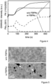
- grazing-incident wide-angle X-ray scattering (GIWAXS) was performed in situ at 150 °C to understand the impact of FBPAc on the perovskite crystallization process. While the crystallization onset of the perovskite (110) and (002) (q ⁇ 10.1 nm -1 ) planes is similar with or without the additive, FBPAc then slows down the perovskite crystallization after 100 s at 150 °C, as showed in figure 4 .
- Perovskite films were then included in 0.25-cm 2 glass/ITO/HTL/perovskite/C 60 /BCP(or SnO 2 )/Cu (or Ag) single junctions to validate with current-voltage (J-V) measurements the improvements induced by FBPAc.
- J-V current-voltage
- the open circuit voltage (V oc ) of the devices improves by 20-30 mV when switching from spiro-TTB to TaTm and Me-4PACz, and by 40-50 mV extra when adding FBPAc.
- the corresponding fill factor (FF) also increases on average from -69 % to -76 % when changing the HTL 7 and then to -78-81 % with the additive.
- PCE power conversion efficiency
- Varying the concentration of FBPAc from 2.5 mM to 7.5 mM in the FABr:FAI solution does not affect the performance significantly with a HTL 7 made of Me-4PACz, as shown in figure 8 .
- perovskite deposition conditions were then adapted to produce 1-cm 2 tandem solar cells on silicon heterojunction (SHJ) bottom cells serving as base layers 3 featuring pyramids of 2-3 ⁇ m height on both sides and a recombination junction on the front side.
- Perovskite layer 9 was made thicker (from -400 nm in single-junctions to -1 ⁇ m) to reach current matching conditions in a tandem with Si with a perovskite Eg of -1.7 eV.
- a CsBr/PbI 2 template of 660 nm thickness was deposited and the spin coating parameters were adapted accordingly.
- the front electrode was made transparent by switching to a stack made of C60 (layer 11), SnOx (lower part of layer 13), indium zinc oxide (IZO) (upper part of layer 13), a Ag grid (layer 15), and a MgF2 antireflective coating (layer 17).
- a V oc of 1.9V could be obtained with either TaTM or Me-4PACz, in line with single-junction and QFLS data.
- the FF of TaTm-based tandems was however significantly lower than with Me-4PACz ( ⁇ 70% compared to >75%), likely as a result of the low hole mobility in undoped TaTm.
- a tandem cell 1 as described above featuring Me-4PACz as HTL 7 and FBPAc as additive in the perovskite precursor solution was sent to the National Renewable Energy Laboratory (NREL) for certification.
- NREL National Renewable Energy Laboratory
- This tandem was slightly top-cell limited and both sub-cells produced a Jsc >20 mA/cm 2 .
- the stabilized J-V properties of the device were measured using the asymptotic maximum power (Pmax) scan method in standard test conditions (STC, 25 °C, 1000 W/m2, AM1.5G spectrum).
- the cell reached a V oc of 1.91 V, a Jsc of 20.47 mA/cm2 and a FF of 79.8%, which resulted in a certified PCE of 31.25% (with an aperture area of 1.1677 cm2).
- the method of the invention improves the crystallinity of the perovskite layer 9, which increases the fill factor of the solar cell 1 due to mitigation of charge transport losses within the perovskite layer since the resulting larger grain structure results in fewer grain boundaries along the travel direction of the charge carriers (i.e. perpendicular to the plane of the perovskite layer 9), increasing the cell efficiency.
- the additive passivates the Pb-related defects present at the top surface of the perovskite layer 9 by coordinating with them on this surface, which increases the open circuit voltage of the solar cell 1 while still enabling charge carrier extraction, further increasing the cell efficiency.
- the approach of the invention is versatile and can be implemented in single-junction opaque cells, single-junction semi-transparent cells, and in tandem cells.
Landscapes
- Physics & Mathematics (AREA)
- Electromagnetism (AREA)
- Engineering & Computer Science (AREA)
- Chemical & Material Sciences (AREA)
- Manufacturing & Machinery (AREA)
- Materials Engineering (AREA)
- Inorganic Chemistry (AREA)
- Photovoltaic Devices (AREA)
Abstract
Description
- The present invention relates to the field of photovoltaic devices. More particularly, it relates to a method of manufacture of a perovskite-based photovoltaic cell.
- Recently, photovoltaic devices (PV devices) based on so-called perovskite absorber layers have been showing promise as an alternative or complement to conventional crystalline and thin-film silicon-based PV devices. "Perovskites" are organometallic halide materials with a formula generically written as ABX3, where A is an inorganic or organic cation such as Cs, CH3NH3 or HC(NH2)2, B is a metal such as tin or lead, and X is a halogen atom such as iodine, bromine or chlorine. Examples of such materials are methylammonium lead trihalide (CH3NH3PbX3), Caesium formamidinum lead trihalide (CsH2NCHNH2PbX3), and methylammonium tin triiodide (CH3NH3SnI3). These compounds adopt a similar crystal structure to calcium titanium oxide (CaTiO3) and, when illuminated, generate electron-hole pairs, which can be separated by sandwiching the perovskite absorber layer between an electron transporting n-type layer and a hole-transporting p-type layer, with the perovskite serving as the intrinsic (i) layer so as to form a PIN or NIP junction, analogous to its silicon counterpart.
- Such perovskite-based cells can be used as single-junction cells, or can be combined with a silicon cell to create a tandem PV device, the perovskite junction being located on the light-incident side of the cell.
- The perovskite layer itself is typically deposited in a wet process, such as wet coating followed by evaporation of the carrier solvent, although vapour deposition techniques are also showing promise. An example of room-temperature solution deposition of perovskite is disclosed in Liu & Kelly, "Perovskite solar cells with a planar heterojunction structure prepared using room-temperature solution processing techniques", Nature Photonics 8, 133-138 (2014).
- Efficiencies of over 25% have been reported with perovskite single junctions, while perovskite/silicon tandems reach 29% in the literature, such as the 29.8% reported by Tockorn et al, "Nano-optical designs for high-efficiency monolithic perovskite-silicon tandem solar cells", Nature Nanotechnology, 17(11), 1214-1221. https://doi.org/10.1038/s41565-022-01228-8 .
- However, Perovskite solar cells are typically limited in performance by i) charge carrier transport losses occurring within the perovskite absorber when reaching a perovskite layer thickness approaching the micrometre scale (that is on the same order of magnitude as the electron and hole diffusion lengths), and ii) by defects that form at the interfaces between the perovskite and the charge carrier selective layers. These voltage losses can be mitigated i) by adapting deposition conditions to yield a perovskite microstructure exhibiting large grains that span across the full perovskite layer thickness, and ii) by developing surface-treatment materials that coordinate with the perovskite surface defects and hence passivate them.
- The microstructure of the perovskite layer can be tuned using a variety of approaches, from fine-tuning the deposition conditions to the use of growth-modulating agents in the perovskite deposition process. The passivation of surface defects is typically achieved by a separate processing step treat an already existing perovskite layer.
- From the scientific literature, phosphonic acids have been used to passivate perovskite solar cells when deposited as a separate, additional step on the perovskite absorber surface, see E. Akman, A. E. Shalan, F. Sadegh, S. Akin, "Moisture-Resistant FAPbl3 Perovskite Solar Cell with 22.25 % Power Conversion Efficiency through Pentafluorobenzyl Phosphonic Acid Passivation" ChemSusChem. 14, 1176-1183 (2021). Although this provides excellent passivation, it requires extra processing steps.
- Document
CN113629196 describes a method of depositing perovskite layers in which phosphonic acids are incorporated in a FA0.85Cs0.15PbI3 perovskite precursor solution applied to the underlying layer of the PV cell by a 1-step spin coating approach as part of the fabrication of an n-i-p configuration photovoltaic cell, followed by annealing for 20 minutes at a temperature of 200°C. The approach enables stabilizing the photoactive FA0.85Cs0.15PbI3 and leads to a chemical modification of the bulk of the perovskite, as highlighted by a shift in bandgap and a larger light absorption range. The relatively high curing temperature used is not suitable for a wide range of perovskite materials as it may lead to their decomposition, which is undesirable. - The aim of the present invention is hence to at least partially overcome the limitations of the prior art.
- More precisely, the invention relates to a method of manufacturing a solar cell, as defined in
independent claim 1. This method comprises at least steps of (further intermediate steps not being excluded): - providing a substrate, which may be an opaque support (e.g. of metal), a transparent support (e.g. of glass, sapphire, transparent polymer or similar) or a silicon solar cell (e.g. a so-called "bottom cell", such that the solar cell of the invention is a tandem cell);
- providing a first layer of transparent conductive oxide directly or indirectly on said substrate;
- providing a first charge transport layer directly or indirectly on said first layer of transparent conductive oxide;
- providing a perovskite-based light-absorber layer directly or indirectly on said first charge transport layer;
- providing a second charge transport layer directly or indirectly on said perovskite-based light absorber layer;
- providing a second layer of transparent conductive oxide directly or indirectly on said second charge transport layer, this typically (but not necessarily) being indirectly provided on the second charge transport layer with a buffer layer (e.g. of atomic layer deposited tin oxide) provided between the two;
- providing a patterned metallic contact layer directly or indirectly on said second layer of transparent conductive oxide.
- According to the invention, said step of providing a perovskite-based light absorber layer comprises:
- providing a perovskite precursor solution comprising an additive comprising an organic phosphonic acid and/or phosphonate salt in a concentration of between 0.1 mMol and 50 mMol, preferably between 1 mMol and 10 mMol depending on the solution, considering the additive with respect to the entirety of the precursor solution;
- applying said perovskite precursor solution directly or indirectly upon said first charge transport layer;
- annealing said perovskite layer at a temperature between 100 °C and 170 °C.
- This additive has been shown to, without requiring any extra fabrication steps:
- increase the fill factor of the solar cell due to improved crystallinity of the perovskite-based light-absorber layer with larger crystal grains, resulting in fewer grain boundaries along the travel direction of the charge carriers;
- improve passivation by binding with Pb-related defects at the top surface of the perovskite-based light-absorber layer, thereby notably increasing the open circuit voltage.
- Advantageously, said first charge transport layer is a hole selective layer comprising one of:
- 2,2',7,7'-Tetra(N,N-di-p-tolyl)amino-9,9-spirobifluorene (spiro-TTB);
- 1,3,4,6-Tetra-O-acetyl-2-O-(trifluoromethanesulfonyl)-beta-D-mannopyranose (TaTm);
- 3,6- dimethyl-9H-carbazol-9-yl)butyl]phosphonic acid (Me-4PACz).
- [2-(3,6-dimethoxy-9H-carbazol-9-yl)ethyl]phosphonic acid (MeO-2PACz)
- [2-(9H-carbazol-9-yl)ethyl]phosphonic acid (2PACz)
- Other suitable materials are possible for the first charge transport layer.
- Advantageously, said second charge transport layer typically comprises carbon-60.
- Advantageously, said additive comprises one or more of: 2,3,4,5,6-pentafluorobenzylphosphonic acid, benzylphosphonic acid, 4-bromobenzylphosphonic acid, 4-fluorobenzylphosphonic acid, (4-chlorophenyl)phosphonic acid, phenylphosphonic acid.
- Advantageously, said perovskite-based light-absorber layer has a thickness between 200 nm and 2000 nm, preferably from 500 to 1500 nm.
- Advantageously, said perovskite-based light absorber layer comprises (Cs,FA,MA)Pb(I,Br,Cl)3 or (Cs,FA)Pb(I,Br,Cl)3, preferably Cs0.18FA0.82Pb(I,Br)3.
- In a one-step deposition process, said perovskite precursor solution comprises organic and inorganic perovskite precursors and is applied directly to said first charge transport layer, i.e. as a single-step deposition. The exact nature of these precursors (such as lead halides (PbI2, PbBr2, PbCl2), cesium halide (Csl, CsBr, CsCI), formamidinium halides (FAI, FABr, FACI) and methylammonium halides (MAI, MABr, MACI), of which PbI2, FAI, PbBr2, FABr, MABr and CsI are preferred) are known to the skilled person and depend on the type of perovskite used for the perovskite-based light absorber layer. In this case, the concentration of said additive in said perovskite precursor solution is preferably 0.1-50 mMol, preferably between 1 and 10 mMol. Furthermore, said substrate may have a roughness of less than 1 µm Ra on a surface facing said perovskite-based light absorber layer.
- In a two-step deposition process, step of providing a perovskite-based light absorber layer comprises a step of vapour depositing a layer of CsX and/or PbX2, where X is I, Br or Cl directly or indirectly on said first charge transport layer followed by said step of applying said perovskite precursor solution. In such a case, said perovskite precursor solution comprises organic perovskite precursors (such as those mentioned above) and is exempt from inorganic perovskite precursors since these were already deposited in the vapour deposition step. In such a case, or indeed also in the case of one-step deposition, said substrate may have a roughness of 0 µm to 10 µm Ra, preferably 2 µm to 10 µm Ra on a surface facing said perovskite-based light absorber layer. Again, the concentration of said additive in said perovskite precursor solution may be from 0.1 mMol to 50 mMol.
- Further details of the description will become clearer upon reading the following description in conjunction with the annexed figures, in which:
-
Figure 1 is a schematic representation of a solar cell produced by the method of the invention; -
Figure 1a is a partial schematic representation of two-step deposition of the perovskite-based light absorber layer on the first charge transport layer; -
Figure 2 is a graph of quasi Fermi-level splitting (QFLS) of bare perovskite layers deposited on glass, on a spiro-TTB hole transport layer (HTL), on a TaTm HTL, and on a Me-4PACz HTL, both with and without use of FBPAc additive, and both with or without use of a C60 electron transport layer (ETL) on the perovskite; -
Figure 3 is a graph of XPS intensity vs binding energy for perovskite films produced with and without FBPAc additive; -
Figure 4 is a graph of grazing incidence wide angle X-ray scattering data showing the evolutions of the (002)/(110) and (001) reflections of the perovskite and PbI2 phases, respectively, during the perovskite crystallization process; -
Figure 5 is a pair of scanning electron microscopy images highlighting the difference in surface morphologies when adding FBPAc additive, with arrows showing additive clusters; -
Figure 6 is four secondary ion mass spectroscopy maps of the 19F- and 12C2- signals, confirming the presence of FBPAc additive in the form of clusters on the surface of the perovskite layer; -
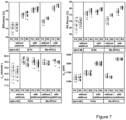
Figure 7 is four graph illustrating performance metrics for solar cells produced with and without FBPAc additive and with various types of hole transport layer materials; -
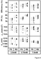
Figure 8 is graphs illustrating that the concentration of FBPAc additive has little impact on performance metrics on a solar cell using Me-4PACz as hole transport layer; and -
Figure 9 is graphs illustrating results obtained by washing the perovskite layer in a solvent which removes FBPAc clusters, thereby proving that it is indeed the presence of the additive which obtains the improvements reported. -
Figure 1 schematically illustrates a solar cell 1 (i.e. a photovoltaic cell) produced by the method of the invention. This can be a single junction perovskite cell, in whichcase substrate 3 is an opaque or transparent support layer such as glass or metal, or a tandem cell, in whichsubstrate 3 is a bottom cell such as (but not limited to) a conventional silicon cell such as a crystalline silicon cell. The upper surface of thesubstrate 3 may be textured, as is generally known and which will be discussed further below. - In the foregoing, it should be noted that each layer can be directly deposited on the previously-formed layer, or may be indirectly deposited thereupon with an intervening layer in between, and the method proceeds from bottom to top in the orientation of
figure 1 . - Upon the
substrate 3, thecell 1 comprises a first transparentconductive oxide layer 5, such as indium tin oxide (ITO), zinc oxide, indium zinc oxide (IZO) or similar. First transparentconductive oxide layer 5 may be doped or undoped. - Upon the first transparent
conductive oxide layer 5, a firstcharge transport layer 7 is deposited. This is either a hole transport (p-type) or an electron transport (n-type) layer, of an applicable type as is generally known in the field of perovskite photovoltaic cells. In the case of a hole transport layer (HTL), spiro-TTB (2,2',7,7'-Tetra(N,N-di-p-tolyl)amino-9,9-spirobifluorene), TaTM (1,3,4,6-Tetra-O-acetyl-2-O-(trifluoromethanesulfonyl)-beta-D-mannopyranose) Me-4PACz (4-(3,6- dimethyl-9H-carbazol-9-yl)butyl]phosphonic acid), -[2-(3,6-dimethoxy-9H-carbazol-9-yl)ethyl]phosphonic acid (MeO-2PACz) or [2-(9H-carbazol-9-yl)ethyl]phosphonic acid (2PACz) are typically used. - Upon the first charge transport layer is deposited a perovskite-based light absorber layer 9 (which can be abbreviated to "
perovskite layer 9" in the context of the present specification), the deposition of which forms the key to the invention as will become more apparent below. This perovskite is typically based on the generic formulae (Cs,FA,MA)Pb(I,Br,Cl)3 or (Cs,FA)Pb(I,Br,Cl)3. Other types of perovskite material are however possible. - Upon the
perovskite layer 9 is deposited a secondcharge transport layer 11, of the opposite type to the firstcharge transport layer 7. This is typically an electron transport layer (ETL) based on carbon-60. - Upon second
charge transport layer 11 is deposited a second layer of transparentconductive oxide 13, which may be a single layer or a multilayer of two different materials, such as one or more of doped or undoped tin oxide, indium tin oxide, indium zinc oxide or similar. Upon this layer is deposited a patternedmetallic contact layer 15 which may comprise is screen-printed silver paste, vapour-deposited copper, or similar, and is typically patterned. A further layer 17 (or indeed layers), such as antireflection layers, can also be deposited on top of the second layer of transparentconductive oxide 13 in the interstices between the patternedmetallic contacts 15. A non-illustrated buffer layer of e.g. atomic layer deposited SnO2 may be deposited between the secondcharge transport layer 12 and the second layer of transparentconductive oxide 13. - However, these examples of materials for the various layers are not to be held as limiting, and the full panoply of suitable materials can be used, as is generally known in the art, provided that the processing temperatures of the
layers perovskite layer 9 do not negatively influence this latter. - The deposition of the
perovskite layer 9 will now be discussed in detail. - This
layer 9 is deposited either in a one-step solution deposition process, or in a two-step process such as that described in F. Sahli, J. Werner, B. A. Kamino, M. Bräuninger, R. Monnard, B. Paviet-Salomon, L. Barraud, L. Ding, J. J. Diaz Leon, D. Sacchetto, G. Cattaneo, M. Despeisse, M. Boccard, S. Nicolay, Q. Jeangros, B. Niesen, C. Ballif, "Fully textured monolithic perovskite/silicon tandem solar cells with 25.2% power conversion efficiency", Nat. Mater. 17, 820-826 (2018), hereby incorporated by reference in its entirety. This two-step process involves a first step of co-evaporating a CsBr/PbI2 template 9a directly or indirectly on the underlying layer, namely the firstcharge transport layer 7, and then solution-depositing theperovskite precursor 9b so as to form theperovskite layer 9. - In both deposition process, a perovskite precursor solution is provided, such precursors being e.g. lead halides (PbX2, where X = I, Br or CI), cesium halides (CsX, where X = I, Br or Cl) formamidinium halides (FAX, where X = I, Br or Cl) and methylammonium halides (MAX, where X = I, Br or Cl) in industry-typical concentrations(0.1 Mol to 2 Mol, see for instance Saliba, M., Correa-Baena, J.-P., Wolff, C. M., Stolterfoht, M., Phung, N., Albrecht, S., Neher, D., & Abate, A. (2018). "How to Make over 20% Efficient Perovskite Solar Cells in Regular ( n-i-p ) and Inverted ( p-i-n ) Architectures." Chemistry of Materials, 30(13), 4193-4201. https://doi.org/10.1021/acs.chemmater.8b00136), to which is added an additive comprising or consisting of an organic phosphonic acid or an organic phosphonate salt such that its concentration in the mixed precursor / additive solution is 0.1 mMol to 50 mMol, preferably 1 mMol to 10 mMol. Typically, 3-7 mMol, further typically substantially 5 mMol additive concentration is used for one-step and two-step depositions. The phosphonic acid or phosphonate salt is dissolved in one or more of a combination of polar and non-polar solvents (such as dimethylformamide (DMF) or dimethylsulfoxide (DMSO), or ethanol) and is added to the perovskite precursors (or, in the case of two-step deposition processes, only to the organic perovskite precursors) up to the desired concentration.
- Such phosphonic acids have the general formula R-PO3H2, where R is any fully or partially fluorinated or non-fluorinated organic functional groups/molecules. A typical example which has shown good results is 2,3,4,5,6-pentafluorobenzylphosphonic acid (FBPAc), but other similar molecules are also possible, such as benzylphosphonic acid, 4-bromobenzylphosphonic acid, 4-fluorobenzylphosphonic acid, (4-chlorophenyl)phosphonic acid and phenylphosphonic acid. These additives may be used individually or in combination.
- In the case of phosphonate salts, these have the general formula R1-PO(OR2)(OR3), where R1 is again any fully or partially fluorinated or non-fluorinated organic functional groups/molecules, R2 and R3 are a cation such as H+, Cs+, K+ or FA+ (i.e. a formamidinium cation).
- After application of the perovskite precursor solution to the surface of the first
charge transport layer 7 by spin coating, dip coating, inkjet printing, meniscus coating, blade coating, slot-die coating, spray coating, or similar, the solvent is allowed to evaporate and the perovskite layer is annealed in ambient or inert gas environment at a temperature of between 100°C and 170°C, preferably between 140°C and 150°C. - The resulting
final perovskite layer 9 thickness is between 200 nm and 2000 nm, preferably between 500 nm and 1500 nm. - In terms of the choice of one step or two step deposition, the former works best with a relatively lightly-textured underlying surface (i.e. the free surface of the first charge transport layer 7), with a roughness typically less than 1 µm Ra. The two-step deposition process, however, provides good results with relatively large textures, of the order of 1-10 µm Ra.
- The additive tunes the growth of the
perovskite layer 9, and segregates on the free surface of this layer during its crystallization to passivate defects and mitigate non-radiative surface recombination losses. - To assess loss pathways triggered by non-radiative recombination, flat glass/indium tin oxide (ITO) substrates were first coated with a hole transport layer 7 (HTL), namely spiro-TTB, TaTM or Me-4PACz. These three materials were selected based on their compatibility with textured surfaces as the first two can be thermally evaporated, while the self-assembling properties (on ITO) of the latter should yield a conformal coating on textured surfaces. A perovskite thin
film perovskite layer 9 of cesium formamidinium lead iodide bromide (Cs0.18FA0.82Pb(I,Br)3) was deposited using the hybrid two-step deposition method referenced above. More precisely, a CsBr/PbI2 template was co-evaporated on glass/ITO substrate, before spin coating an organo-halide solution (consisting of FABr and FAI in various ratios, in some cases with FBPAc). A thermal annealing step in ambient conditions at 150 °C then converted the films into a perovskite phase. In view of making tandem cells, a perovskite composition with an optical Eg of -1.70 eV was selected. -
Figure 2 is a graph of quasi Fermi-level splitting (QFLS) of bare perovskite layers deposited on glass, on a spiro-TTB HTL 7, on aTaTm HTL 7, and on a Me-4PACz HTL 7 (labelled as HTL losses, empty diamonds), both with and without FBPAc additive during solution deposition of theperovskite layer 9, and both with and without aC60 ETL 11 on the perovskite layer (indicated as HTL + ETL losses, filled diamonds). The data is extracted from photoluminescence quantum yield (PLQY) data. This graph clearly shows that QFLS remains substantially constant when incorporating an FBPAc additive. With the presence of anHTL 7, the addition of FBPAc increases the PLQY with all three types ofHTL 7. Overall, QFLS losses are highest on spiro-TTB (-45 to -80 meV compared to the glass/perovskite reference), followed by TaTm (-40 to -65 meV), and lowest on Me-4PACz (-10 to -25 meV). This suggests a better interface quality with Me-4PACz. Without FBPAc, the addition of theC60 ETL 11 on the perovskite leads to significant losses in QFLS (-50 to 100 mV) due to the formation of trap states in the first nm of C60. On the other hand, the incorporation of FBPAc in the perovskite film synthesis mitigates a significant fraction of these losses (+100 mV compared to without FBPAc). X-ray photoelectron spectroscopy (XPS) indicates that this gain in QFLS likely results from an absence of Pb0 surface defects and a shift of the Pb 4f edges when using FBPAc, as shown in the graph offigure 3 . These observations suggest that undercoordinated Pb2+ ions coordinate with the phosphonic group of FBPAc. X-ray diffraction offigure 4 patterns indicate that FBPAc decreases the fraction of PbI2 crystalline phases left at the end of the crystallization process, as shown onfigure 4 . - Starting from a CsBr/PbI2 template 9a freshly spin-coated with FAI/FABr, grazing-incident wide-angle X-ray scattering (GIWAXS) was performed in situ at 150 °C to understand the impact of FBPAc on the perovskite crystallization process. While the crystallization onset of the perovskite (110) and (002) (q~ 10.1 nm-1) planes is similar with or without the additive, FBPAc then slows down the perovskite crystallization after 100 s at 150 °C, as showed in
figure 4 . While proceeding initially with a slower rate, the intensity of these perovskite reflections continues to increase throughout the experiment up to ~400s, an effect not observed without the additive, in which case the peak intensity stabilizes after 150 s at a lower value. This modification of the crystallization pathway by FBPAc results in a more efficient conversion of the CsBr/PbI2 template to a perovskite phase when using FBPAc. Overall, this difference in crystallization kinetics likely originates from the interaction between Pb and FBPAc. - This difference in formation pathway results in films with larger, more monolithic perovskite domains with the additive, as shown by scanning electron microscopy, as illustrated in
figure 5 , in which sub-micrometer black regions are observed on perovskite films featuring FBPAc. From gas field ion source microscopy coupled with secondary ion mass spectroscopy (Figure 6 ), these clusters are rich in F and C and hence indicative of the presence of FBPAc on the perovskite surface, in line with XPS results. On the other hand, films processed without FBPAc do not show any clustering and feature a lower amount of F and C on their surface. FBPAc segregates on the perovskite surface where it coordinates with Pb-related defects (Figure 3 ). - Perovskite films were then included in 0.25-cm2 glass/ITO/HTL/perovskite/C60/BCP(or SnO2)/Cu (or Ag) single junctions to validate with current-voltage (J-V) measurements the improvements induced by FBPAc. As shown in
figure 7 (where FS indicates "forward scan" and RS indicates "reverse scan"), the open circuit voltage (Voc) of the devices improves by 20-30 mV when switching from spiro-TTB to TaTm and Me-4PACz, and by 40-50 mV extra when adding FBPAc. The corresponding fill factor (FF) also increases on average from -69 % to -76 % when changing theHTL 7 and then to -78-81 % with the additive. Overall, the combination of Me-4PACz and FBPAc results in a power conversion efficiency (PCE) of up to 19.5%. Varying the concentration of FBPAc from 2.5 mM to 7.5 mM in the FABr:FAI solution does not affect the performance significantly with aHTL 7 made of Me-4PACz, as shown infigure 8 . Washing the FBPAc islands with a gentle solvent system (cyclohexane and tert-amyl alcohol) to dissolve and remove the FBPAc without otherwise affecting theperovskite layer 9 results in perovskite cells with a similar Voc to that of untreated films, hence highlighting that FBPAc is impacting primarily the recombination at the perovskite top surface and obtaining the improved cell performance, as shown infigure 9 . - The perovskite deposition conditions were then adapted to produce 1-cm2 tandem solar cells on silicon heterojunction (SHJ) bottom cells serving as
base layers 3 featuring pyramids of 2-3 µm height on both sides and a recombination junction on the front side.Perovskite layer 9 was made thicker (from -400 nm in single-junctions to -1 µm) to reach current matching conditions in a tandem with Si with a perovskite Eg of -1.7 eV. For that purpose, a CsBr/PbI2 template of 660 nm thickness was deposited and the spin coating parameters were adapted accordingly. The front electrode was made transparent by switching to a stack made of C60 (layer 11), SnOx (lower part of layer 13), indium zinc oxide (IZO) (upper part of layer 13), a Ag grid (layer 15), and a MgF2 antireflective coating (layer 17). A Voc of 1.9V could be obtained with either TaTM or Me-4PACz, in line with single-junction and QFLS data. The FF of TaTm-based tandems was however significantly lower than with Me-4PACz (<70% compared to >75%), likely as a result of the low hole mobility in undoped TaTm. The impact of a slight change in the perovskite was investigated by changing the FABr:FAI molar ratio from 2, 1.75 and to 1.5. A PCE > 30% could be achieved with different perovskite compositions, with slight variations in Voc Jsc and FF depending on the top cell and the current-limiting sub-cell. - A
tandem cell 1 as described above featuring Me-4PACz asHTL 7 and FBPAc as additive in the perovskite precursor solution was sent to the National Renewable Energy Laboratory (NREL) for certification. This tandem was slightly top-cell limited and both sub-cells produced a Jsc >20 mA/cm2. The stabilized J-V properties of the device were measured using the asymptotic maximum power (Pmax) scan method in standard test conditions (STC, 25 °C, 1000 W/m2, AM1.5G spectrum). The cell reached a Voc of 1.91 V, a Jsc of 20.47 mA/cm2 and a FF of 79.8%, which resulted in a certified PCE of 31.25% (with an aperture area of 1.1677 cm2). - As can be seen from the foregoing, the method of the invention improves the crystallinity of the
perovskite layer 9, which increases the fill factor of thesolar cell 1 due to mitigation of charge transport losses within the perovskite layer since the resulting larger grain structure results in fewer grain boundaries along the travel direction of the charge carriers (i.e. perpendicular to the plane of the perovskite layer 9), increasing the cell efficiency. - The additive passivates the Pb-related defects present at the top surface of the
perovskite layer 9 by coordinating with them on this surface, which increases the open circuit voltage of thesolar cell 1 while still enabling charge carrier extraction, further increasing the cell efficiency. - Since these technical effects are obtained simply by use of an additive in the perovskite precursor solution, no extra manufacturing steps are necessary and the invention can be applied in a standard fabrication process flow, which is extremely interesting from an industrial perspective.
- Finally, the approach of the invention is versatile and can be implemented in single-junction opaque cells, single-junction semi-transparent cells, and in tandem cells.
- Although the invention has been described in terms of specific embodiments, variations thereto are possible without departing from the scope of protection defined by the appended claims.
Claims (15)
- Method of manufacturing a solar cell (1), comprising steps of:- providing a substrate (3);- providing a first layer of transparent conductive oxide (5) on said substrate;- providing a first charge transport layer (7) on said first layer of transparent conductive oxide (5);- providing a perovskite-based light-absorber layer (9) on said first charge transport layer (7);- providing a second charge transport layer (11) on said perovskite-based light absorber layer (9);- providing a second layer of transparent conductive oxide (13) on said second charge transport layer (11);- providing a patterned metallic contact layer (15) on said second layer of transparent conductive oxide (13);characterized in that said step of providing a perovskite-based light absorber layer (9) comprises:- providing a perovskite precursor solution comprising an additive comprising an organic phosphonic acid and/or a phosphonate salt in a concentration of between 0.1 mMol and 50 mMol;- applying said perovskite precursor solution upon said first charge transport layer;- annealing said perovskite layer (9) at a temperature between 100 °C and 170 °C.
- Method according to claim 1, wherein said first charge transport layer (7) is a hole selective layer comprising at least one of:- 2,2',7,7'-Tetra(N,N-di-p-tolyl)amino-9,9-spirobifluorene;- 1,3,4,6-Tetra-O-acetyl-2-O-(trifluoromethanesulfonyl)-beta-D-mannopyranose;- 3,6- dimethyl-9H-carbazol-9-yl)butyl]phosphonic acid;- [2-(3,6-dimethoxy-9H-carbazol-9-yl)ethyl]phosphonic acid;- [2-(9H-carbazol-9-yl)ethyl]phosphonic acid.
- Method according to any preceding claim, wherein said second charge transport layer (11) comprises C60.
- Method according to any preceding claim, wherein said additive comprises one or more of:- 2,3,4,5,6-pentafluorobenzylphosphonic acid;- benzylphosphonic acid,- 4- bromobenzylphosphonic acid,- 4-fluorobenzylphosphonic acid,- (4-chlorophenyl)phosphonic acid,- phenylphosphonic acid.
- Method according to any preceding claim, wherein said perovskite-based light-absorber layer (9) has a thickness between 200 nm and 2000 nm, preferably between 500 nm and 1500 nm.
- Method according to any preceding claim, wherein said perovskite-based light absorber layer (9) comprises (Cs,FA,MA)Pb(I,Br,Cl)3 or (Cs,FA)Pb(I,Br,Cl)3, preferably Cs0.18FA0.82Pb(I,Br)3.
- Method according to any preceding claim, wherein said perovskite precursor solution comprises organic and inorganic perovskite precursors such as combinations of PbI2, PbBr2, PbCl2, CsBr, Csl, CsCI, FAI, FABr, FACI, MAI, MABr, MACI and is applied directly to said first charge transport layer (7).
- Method according to the preceding claim, wherein the concentration of said additive in said perovskite precursor solution is 0.1 mMol - 50 mMol.
- Method according to claim 7 or 8, wherein said substrate (3) has a roughness of less than 1 µm Ra on a surface facing said perovskite-based light absorber layer (9).
- Method according to any of claims 1-6, wherein said step of providing a perovskite-based light absorber layer (9) comprises a step of vapour depositing a layer of CsX and/or PbX2, where X is I, Br, Cl, on said first charge transport layer (7) followed by said step of applying said perovskite precursor solution.
- Method according to claim 10, wherein said perovskite precursor solution comprises organic perovskite precursors such as FAI, FABr, FACI, MAI, MABr, MACI.
- Method according to claim 10 or 11, wherein the concentration of said additive in said perovskite precursor solution is 0.1 mMol - 50 mMol
- Method according to one of claims 10-12, wherein said substrate (3) has a roughness of 0 µm to 10 µm Ra, preferably from 2 µm to 10 µm Ra, on a surface facing said perovskite-based light absorber layer,
- Method according to any preceding claim, wherein said substrate (3) is one of:- an opaque support;- a transparent support;- a silicon solar cell.
- Solar cell obtained or obtainable by the method of any of claims 1-14.
Priority Applications (3)
| Application Number | Priority Date | Filing Date | Title |
|---|---|---|---|
| EP22210577.7A EP4380335A1 (en) | 2022-11-30 | 2022-11-30 | Method of manufacturing a perovskite photovoltaic cell |
| KR1020230168542A KR20240082229A (en) | 2022-11-30 | 2023-11-28 | Method of manufacturing a perovskite photovoltaic cell |
| US18/523,279 US20240180012A1 (en) | 2022-11-30 | 2023-11-29 | Method of manufacturing a perovskite photovoltaic cell |
Applications Claiming Priority (1)
| Application Number | Priority Date | Filing Date | Title |
|---|---|---|---|
| EP22210577.7A EP4380335A1 (en) | 2022-11-30 | 2022-11-30 | Method of manufacturing a perovskite photovoltaic cell |
Publications (1)
| Publication Number | Publication Date |
|---|---|
| EP4380335A1 true EP4380335A1 (en) | 2024-06-05 |
Family
ID=84536148
Family Applications (1)
| Application Number | Title | Priority Date | Filing Date |
|---|---|---|---|
| EP22210577.7A Pending EP4380335A1 (en) | 2022-11-30 | 2022-11-30 | Method of manufacturing a perovskite photovoltaic cell |
Country Status (3)
| Country | Link |
|---|---|
| US (1) | US20240180012A1 (en) |
| EP (1) | EP4380335A1 (en) |
| KR (1) | KR20240082229A (en) |
Citations (2)
| Publication number | Priority date | Publication date | Assignee | Title |
|---|---|---|---|---|
| CN113629196A (en) | 2021-06-17 | 2021-11-09 | 鲁东大学 | Preparation method of stable FACS-based perovskite solar cell |
| CN114497426A (en) * | 2020-10-28 | 2022-05-13 | 南京工业大学 | A method for improving the brightness of a perovskite light-emitting diode and a perovskite light-emitting diode |
Family Cites Families (11)
| Publication number | Priority date | Publication date | Assignee | Title |
|---|---|---|---|---|
| ES2587082T3 (en) * | 2009-12-16 | 2016-10-20 | Heliatek Gmbh | Photoactive building element with organic layers |
| US10038150B2 (en) * | 2011-02-25 | 2018-07-31 | Ecole Polytechnique Federale De Lausanne (Epfl) | Metal complexes for use as dopants and other uses |
| TWI566449B (en) * | 2011-11-30 | 2017-01-11 | 諾瓦發光二極體有限公司 | Organic electronic device and its use |
| EP3002801B1 (en) * | 2014-09-30 | 2018-07-18 | Novaled GmbH | Organic electronic device |
| US10593816B2 (en) * | 2015-01-08 | 2020-03-17 | Korea Research Institute Of Chemical Technology | Method for manufacturing device comprising inorganic/organic hybrid perovskite compound film and device comprising inorganic/organic hybrid perovskite compound film |
| US20180174762A1 (en) * | 2016-12-16 | 2018-06-21 | Uchicago Argonne, Llc | Hybrid organic-inorganic electron selective overlayers for halide perovoskites |
| US11094884B2 (en) * | 2018-01-12 | 2021-08-17 | The Board Of Trustees Of The University Of Alabama | Rapid metal oxide layer-specific photonic treatment using UV LED for fabrication of flexible perovskite structures |
| CN116686423A (en) * | 2021-02-10 | 2023-09-01 | 高峰 | Preparation method of device transport material composition, composition, transport layer comprising same, and electronic device comprising transport layer |
| EP4292144B1 (en) * | 2021-02-12 | 2026-01-21 | First Solar, Inc. | Materials and methods for hole transport layers in perovskite photovoltaic devices |
| DE102021201746A1 (en) * | 2021-02-24 | 2022-08-25 | Karlsruher Institut für Technologie | Perovskite-based multi-junction solar cell and method for its manufacture |
| EP4145547A1 (en) * | 2021-09-03 | 2023-03-08 | Saule S.A. | Perovskite solar cell |
-
2022
- 2022-11-30 EP EP22210577.7A patent/EP4380335A1/en active Pending
-
2023
- 2023-11-28 KR KR1020230168542A patent/KR20240082229A/en active Pending
- 2023-11-29 US US18/523,279 patent/US20240180012A1/en active Pending
Patent Citations (2)
| Publication number | Priority date | Publication date | Assignee | Title |
|---|---|---|---|---|
| CN114497426A (en) * | 2020-10-28 | 2022-05-13 | 南京工业大学 | A method for improving the brightness of a perovskite light-emitting diode and a perovskite light-emitting diode |
| CN113629196A (en) | 2021-06-17 | 2021-11-09 | 鲁东大学 | Preparation method of stable FACS-based perovskite solar cell |
Non-Patent Citations (7)
| Title |
|---|
| AKMAN ERDI ET AL: "Moisture-Resistant FAPbI 3 Perovskite Solar Cell with 22.25?% Power Conversion Efficiency through Pentafluorobenzyl Phosphonic Acid Passivation", CHEMSUSCHEM, vol. 14, no. 4, 19 January 2021 (2021-01-19), DE, pages 1176 - 1183, XP093041345, ISSN: 1864-5631, DOI: 10.1002/cssc.202002707 * |
| E. AKMANA. E. SHALANF. SADEGHS. AKIN: "Moisture-Resistant FAPbl3 Perovskite Solar Cell with 22.25 % Power Conversion Efficiency through Pentafluorobenzyl Phosphonic Acid Passivation", CHEMSUSCHEM, vol. 14, 2021, pages 1176 - 1183 |
| F. SAHLIJ. WERNERB. A. KAMINOM. BRAUNINGERR. MONNARDB. PAVIET-SALOMONL. BARRAUDL. DINGJ. J. DIAZ LEOND. SACCHETTO: "Fully textured monolithic perovskite/silicon tandem solar cells with 25.2% power conversion efficiency", NAT. MATER., vol. 17, 2018, pages 820 - 82 |
| HO-BAILLIE ANITA W Y ET AL: "Recent progress and future prospects of perovskite tandem solar cells", APPLIED PHYSICS REVIEWS, AMERICAN INSTITUTE OF PHYSICS, 2 HUNTINGTON QUADRANGLE, MELVILLE, NY 11747, vol. 8, no. 4, 15 October 2021 (2021-10-15), XP012260444, DOI: 10.1063/5.0061483 * |
| LI XIONG ET AL: "Improved performance and stability of perovskite solar cells by crystal crosslinking with alkylphosphonic acid [omega]-ammonium chlorides", NATURE CHEMISTRY, vol. 7, no. 9, 17 August 2015 (2015-08-17), London, pages 703 - 711, XP093041344, ISSN: 1755-4330, DOI: 10.1038/nchem.2324 * |
| SUNG SAE JIN ET AL: "Molecular Engineering for Function-Tailored Interface Modifier in High-Performance Perovskite Solar Cells", ADVANCED ENERGY MATERIALS, vol. 12, no. 27, 30 May 2022 (2022-05-30), DE, pages 2200758, XP093041347, ISSN: 1614-6832, DOI: 10.1002/aenm.202200758 * |
| TOCKORN ET AL.: "Nano-optical designs for high-efficiency monolithic perovskite-silicon tandem solar cells", NATURE NANOTECHNOLOGY, vol. 17, no. 11, pages 1214 - 1221, Retrieved from the Internet <URL:https://doi.org/10.1038/s41565-022-01228-8> |
Also Published As
| Publication number | Publication date |
|---|---|
| KR20240082229A (en) | 2024-06-10 |
| US20240180012A1 (en) | 2024-05-30 |
Similar Documents
| Publication | Publication Date | Title |
|---|---|---|
| CN112086535B (en) | Laminated battery | |
| CN116133448B (en) | A perovskite-silicon tandem solar cell and its fabrication method | |
| US9564593B2 (en) | Solar cells comprising 2d-perovskites | |
| CN114267789B (en) | Method for simultaneously improving open-circuit voltage and stability of full-suede perovskite/crystalline silicon laminated solar cell | |
| Zhou et al. | Solution-processed Cu-doped SnO2 as an effective electron transporting layer for high-performance planar perovskite solar cells | |
| CN107710434A (en) | Photovoltaic installation | |
| KR102496459B1 (en) | Perovskite/Gallium Arsenide tandem type solar cell and preparation method thereof | |
| US11174276B2 (en) | Organic-inorganic perovskite materials and methods of making the same | |
| CN114335359B (en) | A method for manufacturing a perovskite film, a solar cell and a stacked cell | |
| CN112086534A (en) | Laminated battery and method of making the same | |
| EP4665124A1 (en) | Solar cell and preparation method therefor | |
| WO2023097365A1 (en) | Tandem photovoltaic cell | |
| US12300446B2 (en) | Multijunction photovoltaic devices with metal oxynitride layer | |
| CN119300618A (en) | Perovskite solar cell, preparation method and prepared laminated perovskite solar cell | |
| US20250008755A1 (en) | Perovskite photovoltaic devices and methods of manufacturing thereof | |
| US20240180012A1 (en) | Method of manufacturing a perovskite photovoltaic cell | |
| WO2026020673A1 (en) | Tandem solar cell and preparation method therefor | |
| CN118678704A (en) | Solar cell, preparation method thereof, photovoltaic module and photovoltaic system | |
| Sahli et al. | Hybrid sequential deposition process for fully textured perovskite/silicon tandem solar cells | |
| KR102761911B1 (en) | Method of manufacturing tandem solar cell | |
| CN222090033U (en) | Stacked solar cell and electricity utilization device | |
| EP4535967A1 (en) | Wide bandgap perovskite | |
| Okamoto | Production and efficiency improvement of perovskite solar cells using the new 3-step method | |
| CN122028634A (en) | B-site Cd-doped two-dimensional perovskite thin film and perovskite/crystalline silicon laminated solar cell | |
| WO2025207945A1 (en) | Precursor solutions for perovskite solar cells |
Legal Events
| Date | Code | Title | Description |
|---|---|---|---|
| PUAI | Public reference made under article 153(3) epc to a published international application that has entered the european phase |
Free format text: ORIGINAL CODE: 0009012 |
|
| STAA | Information on the status of an ep patent application or granted ep patent |
Free format text: STATUS: THE APPLICATION HAS BEEN PUBLISHED |
|
| AK | Designated contracting states |
Kind code of ref document: A1 Designated state(s): AL AT BE BG CH CY CZ DE DK EE ES FI FR GB GR HR HU IE IS IT LI LT LU LV MC ME MK MT NL NO PL PT RO RS SE SI SK SM TR |
|
| STAA | Information on the status of an ep patent application or granted ep patent |
Free format text: STATUS: REQUEST FOR EXAMINATION WAS MADE |
|
| 17P | Request for examination filed |
Effective date: 20241121 |
|
| RBV | Designated contracting states (corrected) |
Designated state(s): AL AT BE BG CH CY CZ DE DK EE ES FI FR GB GR HR HU IE IS IT LI LT LU LV MC ME MK MT NL NO PL PT RO RS SE SI SK SM TR |
|
| RAP3 | Party data changed (applicant data changed or rights of an application transferred) |
Owner name: CSEM CENTRE SUISSE D'ELECTRONIQUE ET DEMICROTECHNIQUE SA - RECHERCHE ET DEVELOPPEMENT |