EP4380044A1 - Integrated transimpedance amplifier with a digital signal processor for high-speed optical receivers - Google Patents
Integrated transimpedance amplifier with a digital signal processor for high-speed optical receivers Download PDFInfo
- Publication number
- EP4380044A1 EP4380044A1 EP23207512.7A EP23207512A EP4380044A1 EP 4380044 A1 EP4380044 A1 EP 4380044A1 EP 23207512 A EP23207512 A EP 23207512A EP 4380044 A1 EP4380044 A1 EP 4380044A1
- Authority
- EP
- European Patent Office
- Prior art keywords
- circuitry
- dsp
- amplifier
- circuit
- tia
- Prior art date
- Legal status (The legal status is an assumption and is not a legal conclusion. Google has not performed a legal analysis and makes no representation as to the accuracy of the status listed.)
- Pending
Links
Images

Classifications
-
- H—ELECTRICITY
- H03—ELECTRONIC CIRCUITRY
- H03F—AMPLIFIERS
- H03F3/00—Amplifiers with only discharge tubes or only semiconductor devices as amplifying elements
- H03F3/45—Differential amplifiers
- H03F3/45071—Differential amplifiers with semiconductor devices only
- H03F3/45076—Differential amplifiers with semiconductor devices only characterised by the way of implementation of the active amplifying circuit in the differential amplifier
- H03F3/45475—Differential amplifiers with semiconductor devices only characterised by the way of implementation of the active amplifying circuit in the differential amplifier using IC blocks as the active amplifying circuit
-
- H—ELECTRICITY
- H03—ELECTRONIC CIRCUITRY
- H03F—AMPLIFIERS
- H03F1/00—Details of amplifiers with only discharge tubes, only semiconductor devices or only unspecified devices as amplifying elements
- H03F1/08—Modifications of amplifiers to reduce detrimental influences of internal impedances of amplifying elements
-
- G—PHYSICS
- G01—MEASURING; TESTING
- G01J—MEASUREMENT OF INTENSITY, VELOCITY, SPECTRAL CONTENT, POLARISATION, PHASE OR PULSE CHARACTERISTICS OF INFRARED, VISIBLE OR ULTRAVIOLET LIGHT; COLORIMETRY; RADIATION PYROMETRY
- G01J1/00—Photometry, e.g. photographic exposure meter
- G01J1/42—Photometry, e.g. photographic exposure meter using electric radiation detectors
- G01J1/44—Electric circuits
-
- H—ELECTRICITY
- H03—ELECTRONIC CIRCUITRY
- H03F—AMPLIFIERS
- H03F3/00—Amplifiers with only discharge tubes or only semiconductor devices as amplifying elements
- H03F3/04—Amplifiers with only discharge tubes or only semiconductor devices as amplifying elements with semiconductor devices only
- H03F3/08—Amplifiers with only discharge tubes or only semiconductor devices as amplifying elements with semiconductor devices only controlled by light
- H03F3/087—Amplifiers with only discharge tubes or only semiconductor devices as amplifying elements with semiconductor devices only controlled by light with IC amplifier blocks
-
- H—ELECTRICITY
- H03—ELECTRONIC CIRCUITRY
- H03F—AMPLIFIERS
- H03F3/00—Amplifiers with only discharge tubes or only semiconductor devices as amplifying elements
- H03F3/189—High-frequency amplifiers, e.g. radio frequency amplifiers
- H03F3/19—High-frequency amplifiers, e.g. radio frequency amplifiers with semiconductor devices only
- H03F3/195—High-frequency amplifiers, e.g. radio frequency amplifiers with semiconductor devices only in integrated circuits
-
- H—ELECTRICITY
- H03—ELECTRONIC CIRCUITRY
- H03G—CONTROL OF AMPLIFICATION
- H03G3/00—Gain control in amplifiers or frequency changers
- H03G3/20—Automatic control
- H03G3/30—Automatic control in amplifiers having semiconductor devices
-
- H—ELECTRICITY
- H03—ELECTRONIC CIRCUITRY
- H03G—CONTROL OF AMPLIFICATION
- H03G3/00—Gain control in amplifiers or frequency changers
- H03G3/20—Automatic control
- H03G3/30—Automatic control in amplifiers having semiconductor devices
- H03G3/3084—Automatic control in amplifiers having semiconductor devices in receivers or transmitters for electromagnetic waves other than radiowaves, e.g. lightwaves
-
- H—ELECTRICITY
- H04—ELECTRIC COMMUNICATION TECHNIQUE
- H04B—TRANSMISSION
- H04B10/00—Transmission systems employing electromagnetic waves other than radio-waves, e.g. infrared, visible or ultraviolet light, or employing corpuscular radiation, e.g. quantum communication
- H04B10/60—Receivers
- H04B10/66—Non-coherent receivers, e.g. using direct detection
- H04B10/69—Electrical arrangements in the receiver
- H04B10/693—Arrangements for optimizing the preamplifier in the receiver
- H04B10/6931—Automatic gain control of the preamplifier
-
- H—ELECTRICITY
- H03—ELECTRONIC CIRCUITRY
- H03F—AMPLIFIERS
- H03F2200/00—Indexing scheme relating to amplifiers
- H03F2200/372—Noise reduction and elimination in amplifier
-
- H—ELECTRICITY
- H03—ELECTRONIC CIRCUITRY
- H03G—CONTROL OF AMPLIFICATION
- H03G2201/00—Indexing scheme relating to subclass H03G
- H03G2201/10—Gain control characterised by the type of controlled element
- H03G2201/103—Gain control characterised by the type of controlled element being an amplifying element
Definitions
- the present description relates generally to optical communications including, for example, a complementary metal-oxide semiconductor (CMOS) integrated transimpedance amplifier (TIA) integrated with a digital signal processor (DSP) for high-speed optical receivers.
- CMOS complementary metal-oxide semiconductor
- TIA complementary metal-oxide semiconductor
- DSP digital signal processor
- Current optical modules include stand-alone TIAs and are generally cost and power sensitive.
- the stand-alone bipolar TIA that is used in the optical modules can be responsible for a relatively large portion of the total cost and power consumption of the optical module.
- Attempts to integrate CMOS TIA with DSP to reduce one relatively small chip from a circuit board generally result in weak performance of the CMOS TIA, resulting in a bottleneck that prevents CMOS TIA integration from being used for high-end, ultra-high-speed (e.g., 400 Gigahertz or 400G) optical modules for high-speed applications.
- ultra-high-speed e.g. 400 Gigahertz or 400G
- an optical module includes a CMOS TIA circuit integrated with a DSP circuit.
- the CMOS TIA can be co-designed and merged with a DSP circuit in a receiver system to achieve a desired overall performance.
- optimal modules described herein can eliminate the need for interconnections (e.g., bond wire, trace(s)) commonly found on a circuit board and located between a stand-alone TIA circuit and a stand-alone DSP circuit.
- optical modules described herein may be used in high-speed applications, including 400G applications. Accordingly, optical modules described herein may include 400G DR4 modules.
- the bandwidth of the TIA circuit can be adjusted, using the DSP circuit, and optimized for the overall receiver system bit-error rate (BER) as compared to using the output of stand-alone TIA circuits.
- BER bit-error rate
- FFE feed-forward equalization
- DFE decision-feedback equalization
- TIA circuits includes adaptation by DSP to accommodate various environments.
- a TIA circuit may be required to communicate with different transmitters, through different channels, under process-voltage-temperature (PVT) corners, and input optical-modulation amplitudes (OMAs).
- PVT process-voltage-temperature
- OMAs input optical-modulation amplitudes
- the disclosed TIA circuits have several digitally controlled knobs to adapt its transfer function (frequency response) shape based on information provided by the DSP circuits.
- the DSP-assisted design can finely adapt the TIA circuit to find the desired performance in all situations, and transition the TIA transfer function when PVT or input signal has changed.
- the subject technology further allows power supply adaptation by DSP circuit to achieve a desired performance and power.
- the DSP circuit can control the power supply of analog front-end to optimize TIA performance and power consumption, based on DSP circuit information.
- the disclosed solution allows adaptive gain allocation for best noise and total harmonic distortion (THD) trade-off to better balance the impact from the noise and THD, therefore, to achieve a desired overall performance.
- THD total harmonic distortion
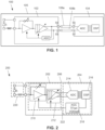
- FIG. 1 illustrates a schematic diagram illustrating an example of a receiver system 100 with a stand-alone TIA circuit 102, according to one approach.
- the stand-alone TIA 102 circuit e.g., a chip or a die
- a stand-alone DSP circuit 104 e.g., a chip or a die
- the receiver system 100 is an existing solution, in which the stand-alone TIA circuit 102 is connected to the stand-alone DSP 104 via an interconnection 108a and an interconnection 108b.
- Each of the interconnections 108a and 108b terminates at 50-Ohm connections, i.e., 50-Ohm impedance pads.
- the interconnections 108a and 108b may include bond wires and/or traces on the circuit board 105. As shown, the interconnections 108a and 108b lie outside of the stand-alone TIA circuit 102 and the stand-alone DSP circuit 104.
- the interconnections 108a and 108b represent chip-to-chip connections or chip-to-package connections between the stand-alone TIA circuit 102 and the stand-alone DSP circuit 104.
- the interconnections 108a and 108b can prevent optimization of the stand-alone TIA circuit 102 by the stand-alone DSP circuit 104.
- the stand-alone DSP circuit 104 is unable to provide commands or feedback used to control or optimize the stand-alone TIA circuit 102, and the stand-alone TIA circuit 102 may only be able to self-optimize or self-control.
- the interconnection 108a and 108b need to connect to 50-Ohm impedance pads on the stand-alone TIA circuit 102 and stand-alone DSP circuit 104.
- the receiver system 100 may be susceptible to performance issues due to, for instance, power reflection and crosstalk, attenuation of the interconnections 108a and 108b, and may require matching impedance at the output nodes of the stand-alone TIA circuit 102 and the input nodes of the stand-alone DSP circuit 104.
- FIG. 2 illustrates a schematic diagram of a receiver system 200 with an integrated amplifier circuit, according to aspects of the subject technology.
- the receiver system 200 may be used in a high-speed optical module (e.g., operating at approximately 4X100 Gigabytes per second, or Gbps).
- the receiver system 200 includes an amplifier circuit 202 and a DSP circuit 204 integrated on a substrate 206, representing a single chip or single integrated circuit.
- the amplifier circuit 202 is a TIA circuit.
- the amplifier circuit 202 operates at 100 Gbps.
- the amplifier circuit includes a CMOS TIA. Using CMOS technology, an amplifier circuit (e.g., amplifier circuit 202) can use transistors in digital circuit applications.
- the amplifier circuit 202 and the DSP circuit 204 are electrically connected to each other in part by placing both the amplifier circuit 202 and the DSP circuit 204 onto a single chip. Additionally, the amplifier circuit 202 and the DSP circuit 204 are connected (e.g., electrically connected) on the substrate 206 without a connection(s) (e.g., interconnections 108a and 108b of FIG. 1 ) on the substrate 206 (e.g., without using impedance pads).
- the substrate 206 lacks interconnections (and associated impedance issues using the impedance pads) between the amplifier circuit 202 and the DSP circuit 204, and the DSP circuit 204 can provide commands, controls, and/or feedback to the amplifier circuit 202 in order to optimize and enhance performance of the amplifier circuit 202.
- the amplifier circuit 202 is CMOS TIA, and may include a front stage 210 including a variable-feedback resistor R v and an amplifier, and a later stage 212 that includes a variable gain amplifier (VGA), including a 3-stage VGA.
- the DSP circuit 204 includes an analog-to-digital converter (ADC) 214, a DSP module 216, and an automatic gain control (AGC) unit 218.
- ADC analog-to-digital converter
- the ADC 214 converts the analog output of the amplifier circuit 202 to a digital signal for processing by the DSP module 216.
- the inputs of the ADC 214 are relatively high-impedance (Z) inputs, thereby allowing the output of the amplifier circuit 202 to have any arbitrary output impedance.
- the AGC unit 218 can provide a relative constant output amplitude despite a varying incoming input.
- the ACG unit 218 may adapt and optimize a transfer function of the amplifier circuit 202 and/or provide and regulate supply voltage to the amplifier circuit 202. This will be further discussed below.
- a path 222 from the DSP circuit 204 to the amplifier circuit 202 can be used by the DSP circuit 204 to provide information such transfer function optimization information based upon changes in transmitter modules, channel status, temperature, voltage, process variation, and channel status.
- the path 222 can provide feedback to the front stage 210 and to the later stage 212.
- the path 222 be used the DSP circuit 204 to provide and regulate supply voltage to the amplifier circuit 202, and in particular, to the front stage 210 and to the later stage 212.
- the receiver system 200 further includes a photodetector block 220, which includes a photoelectric converter that converts received optical signals (from a transmitter, not shown) into electrical signals, with the electrical signals being provided to the amplifier circuit 202.
- the amplifier circuit 202 can work in conjunction with the photodetector block 220 and be compatible with different transmitters, photodiodes, and optical fibers.
- the amplifier circuit 202 in conjunction with controls and/or feedback from the DSP circuit 204, can adapt to transmitters, photodiodes, and/or optical fibers with different specifications (e.g., voltage requirements, current requirements) and from different manufacturers.
- the receiver system 200 may include enhanced system performance when used with optical modules (including high-speed optical modules), as the need for an interconnection between the amplifier circuit 202 and the DSP circuit 204 is eliminated due to the integration of the amplifier circuit 202 with the DSP circuit 204. Without an interconnection(s) between the amplifier circuit 202 and the DSP circuit 204, performance improvements may include fewer reflections, fewer attenuations, and no matching impedance at both TIA output and the receiver input associated with the existing stand-alone TIA and the receiver DSP. Additionally, by removing interconnections and merging the amplifier circuit 202 with the DSP circuit 204 into a single integration, the overall footprint of the receiver system 200 may be reduced.
- one or more parameters can be adjusted/controlled by a signal (e.g., control signal) provided the DSP circuit 204 to the amplifier circuit 202 for the overall receiver system BER instead of using quality of the output of the amplifier circuit 202.
- a signal e.g., control signal
- the receiver system 200 can fully utilize the capability of FFE and DFE in the DSP circuit 204.
- Stand-alone TIA e.g., stand-alone TIA circuit 102, shown in FIG. 1
- sets their own bandwidth & transfer function so a (separate) DSP circuit (e.g., stand-alone DSP circuit 104, shown in FIG.
- a DSP circuit e.g., DSP circuit 204 will be able to fully utilize its equalization capability to achieve the best system performance, especially for DFE as it is a noise-free equalizer.
- FIG. 3 illustrates transfer function plots 330, according to aspects of the subject technology.
- An amplifier circuit e.g., amplifier circuit 202
- DSP circuit e.g., DSP circuit 204 of FIG. 2
- This may include, for example, the AGC unit 218.
- the transfer function plots 330 include various charts depicting the types of modifications and adaptations to a transfer function of an amplifier circuit. For example, a chart 332 shows a low-frequency gain of the transfer function changed based on the information provided by a DSP circuit.
- the plot 334 and the plot 336 show changing of a mid-frequency gain and a high-frequency gain, respectively, of the transfer function of an amplifier circuit based on the information provided by a DSP circuit.
- the plot 338 shows a change of the shape of the transfer function of a TIA circuit as a shift upward or a shift downward based on information provided by a DSP circuit.
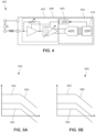
- FIG. 4 is a schematic diagram illustrating an example of a receiver system 400 with DSP power supply control, according to aspects of the subject technology.
- the receiver system 400 represents a high-speed optical receiver (e.g., operating at approximately 4X100 Gbps).
- the receiver system 400 includes an amplifier circuit 402 and a DSP circuit 404 integrated onto a substrate 406, similar to the amplifier circuit 202, the DSP circuit 204, and the substrate 206, respectively, of FIG. 2 .
- the receiver system 400 includes a power supply 440.
- the power supply 440 is implemented by a low-dropout regulator, or LDO regulator.
- the power supply 440 when implemented as an LDO regulator, can regulate an output voltage from a relatively higher input voltage in digital circuits.
- the power supply 440 can provide and regulate power to the amplifier circuit 402.
- the DSP circuit 404 (including a DSP unit 416) can provide commands and other information to the power supply 440, and as a result, can improve performance and reduce power consumption of the amplifier circuit 402.
- FIG. 5A and 5B illustrate example plots depicting adaptive gain control to balance noise and THD of a receiver system with an integrated amplifier circuit (e.g., TIA circuit), according to aspects of the subject technology.
- the performance of the front-end circuit of an optical receiver can be limited either by the noise or the THD.
- the noise and THD usually co-exist as a trade-off to each other.
- the noise is the dominant factor, and when input signal is large, the THD can have the greater influence on the performance of the optical receiver.
- reducing the system noise can be achieved by allocating more gain to the front stages, and reducing the system THD can be accomplished by allocating more gain to later stages.
- the gain could be allocated properly between the front and later stages to best balance the impact from the noise and THD.
- the gain of the TIA circuit output could be allocated properly between the front stage (e.g., front stage 210 of FIG. 2 ) and later stage (e.g., later stage 212 of FIG. 2 ) to balance the impact from the noise and THD, therefore, to achieve a desired overall performance.
- the chart 550 in FIG. 5A is associated with a noise adjustment (optimization) scenario and includes a plot 552, a plot 554 and a plot 556.
- the plot 552 represents an overall transfer function, while the plots 554 and 556 represent transfer functions (frequency responses) of the gains of the front stage and a later stage, respectively, of an amplifier circuit. For this scenario (noise adjustment) the greater gain is allocated to the front stage to counter the effect of the noise.
- the plot 552 depicts an overall transfer function, which is the product of the two transfer functions shown by the plots 554 and 556.
- the chart 560 in FIG. 5B is associated with a THD adjustment scenario and includes a plot 562, a plot 564 and a plot 566.
- the plots 564 and 566 represent transfer functions of the gains of the front stage and a later stage, respectively, of an amplifier circuit. For this scenario, the greater gain is allocated to later stages of the amplifier circuit to counter the effect of the THD.
- the plot 562 depicts an overall transfer function, which is the product of the two transfer functions shown by the plots 564 and 566.
- a processor configured to monitor and control an operation or a component may also mean the processor being programmed to monitor and control the operation or the processor being operable to monitor and control the operation.
- a processor configured to execute code can be construed as a processor programmed to execute code or operable to execute code.
- a phrase such as an "aspect” does not imply that such aspect is essential to the subject technology, or that such aspect applies to all configurations of the subject technology.
- a disclosure relating to an aspect may apply to all configurations, or one or more configurations.
- a phrase such as an “aspect” may refer to one or more aspects, and vice versa.
- a phrase such as a “configuration” does not imply that such configuration is essential to the subject technology, or that such configuration applies to all configurations of the subject technology.
- a disclosure relating to a configuration may apply to all configurations, or one or more configurations.
- a phrase such as a "configuration” may refer to one or more configurations, and vice versa.
- example is used herein to mean “serving as an example or illustration.” Any aspect or design described herein as “example” is not necessarily to be construed as preferred or advantageous over other aspects or designs.
- the phrase "at least one of” preceding a series of items, with the term “and” or “or” to separate any of the items, modifies the list as a whole, rather than each member of the list (i.e., each item).
- the phrase "at least one of” does not require selection of at least one of each item listed; rather, the phrase allows a meaning that includes at least one of any one of the items, and/or at least one of any combination of the items.
- the phrases “at least one of A, B, and C" or “at least one of A, B, or C” each refer to only A, only B, or only C; and/or any combination of A, B, and C. In instances where it is intended that a selection be of "at least one of each of A, B, and C," or alternatively, "at least one of A, at least one of B, and at least one of C,” it is expressly described as such.
Landscapes
- Engineering & Computer Science (AREA)
- Power Engineering (AREA)
- Physics & Mathematics (AREA)
- Electromagnetism (AREA)
- General Physics & Mathematics (AREA)
- Spectroscopy & Molecular Physics (AREA)
- Microelectronics & Electronic Packaging (AREA)
- Computer Networks & Wireless Communication (AREA)
- Signal Processing (AREA)
- Amplifiers (AREA)
Abstract
Description
- This application is a continuation of and claims priority to and the benefit of
U.S. Patent Application No. 17/980,478, titled "INTEGRATED TRANSIMPEDANCE AMPLIFIER WITH A DIGITAL SIGNAL PROCESSOR FOR HIGH-SPEED OPTICAL RECEIVERS," and filed on November 3, 2022 - The present description relates generally to optical communications including, for example, a complementary metal-oxide semiconductor (CMOS) integrated transimpedance amplifier (TIA) integrated with a digital signal processor (DSP) for high-speed optical receivers.
- Current optical modules include stand-alone TIAs and are generally cost and power sensitive. The stand-alone bipolar TIA that is used in the optical modules can be responsible for a relatively large portion of the total cost and power consumption of the optical module. Attempts to integrate CMOS TIA with DSP to reduce one relatively small chip from a circuit board generally result in weak performance of the CMOS TIA, resulting in a bottleneck that prevents CMOS TIA integration from being used for high-end, ultra-high-speed (e.g., 400 Gigahertz or 400G) optical modules for high-speed applications.
- Certain features of the subject technology are set forth in the appended claims. However, for purposes of explanation, several aspects of the subject technology are depicted in the following figures.
-
FIG. 1 illustrates a circuit diagram illustrating an example of a receiver system with a stand-alone TIA circuit. -
FIG. 2 illustrates a circuit diagram illustrating an example of a receiver system with an integrated amplifier circuit, according to aspects of the subject technology. -
FIG. 3 illustrates corresponding transfer function plots, according to aspects of the subject technology. -
FIG. 4 illustrates a circuit diagram illustrating an example of a receiver system with DSP power supply control, according to aspects of the subject technology. -
FIGS. 5A and 5B illustrate example plots depicting adaptive gain control to balance noise and total harmonic distortion (THD) of a receiver system with integrated TIA, according to aspects of the subject technology. - The detailed description set forth below is intended as a description of various configurations of the subject technology and is not intended to represent the only configurations in which the subject technology may be practiced. The appended drawings are incorporated herein and constitute a part of the detailed description. The detailed description includes specific details for the purpose of providing a thorough understanding of the subject technology. However, the subject technology is not limited to the specific details set forth herein and may be practiced using one or more implementations. In one or more instances, structures and components are shown in block-diagram form in order to avoid obscuring the concepts of the subject technology.
- According to some aspects, the subject technology is directed to optical modules used in high speed optical data transfer applications. Optical modules described herein are used in the conversion of electrical signals into optical signals, and vice versa. In some embodiments, an optical module includes a CMOS TIA circuit integrated with a DSP circuit. The CMOS TIA can be co-designed and merged with a DSP circuit in a receiver system to achieve a desired overall performance. By integrating the CMOS TIA with the DSP onto, for example, an integrated circuit, optimal modules described herein can eliminate the need for interconnections (e.g., bond wire, trace(s)) commonly found on a circuit board and located between a stand-alone TIA circuit and a stand-alone DSP circuit. As a result, the system performance is enhanced through fewer deflections, losses, and crosstalk. Moreover, as a result of TIA circuit integration and merger with a DSP circuit, optical modules described herein may be used in high-speed applications, including 400G applications. Accordingly, optical modules described herein may include 400G DR4 modules.
- Further, by integrating the CMOS TIA circuit with the DSP circuit, the bandwidth of the TIA circuit can be adjusted, using the DSP circuit, and optimized for the overall receiver system bit-error rate (BER) as compared to using the output of stand-alone TIA circuits. This allows the capability of feed-forward equalization (FFE) and decision-feedback equalization (DFE) in DSP to be fully utilized.
- Another aspect of the disclosed TIA circuits includes adaptation by DSP to accommodate various environments. For example, a TIA circuit may be required to communicate with different transmitters, through different channels, under process-voltage-temperature (PVT) corners, and input optical-modulation amplitudes (OMAs). The disclosed TIA circuits have several digitally controlled knobs to adapt its transfer function (frequency response) shape based on information provided by the DSP circuits. The DSP-assisted design can finely adapt the TIA circuit to find the desired performance in all situations, and transition the TIA transfer function when PVT or input signal has changed.
- The subject technology further allows power supply adaptation by DSP circuit to achieve a desired performance and power. The DSP circuit can control the power supply of analog front-end to optimize TIA performance and power consumption, based on DSP circuit information. Furthermore, the disclosed solution allows adaptive gain allocation for best noise and total harmonic distortion (THD) trade-off to better balance the impact from the noise and THD, therefore, to achieve a desired overall performance.
-
FIG. 1 illustrates a schematic diagram illustrating an example of areceiver system 100 with a stand-alone TIA circuit 102, according to one approach. As shown, the stand-alone TIA 102 circuit (e.g., a chip or a die) and a stand-alone DSP circuit 104 (e.g., a chip or a die) are each located on a circuit board 105 (e.g., printed circuit board). Thereceiver system 100 is an existing solution, in which the stand-alone TIA circuit 102 is connected to the stand-alone DSP 104 via aninterconnection 108a and aninterconnection 108b. Each of theinterconnections interconnections circuit board 105. As shown, theinterconnections alone TIA circuit 102 and the stand-alone DSP circuit 104. Theinterconnections alone TIA circuit 102 and the stand-alone DSP circuit 104. - Based on the stand-
alone TIA circuit 102 and theinterconnections receiver system 100 may be limited. Also, theinterconnections alone TIA circuit 102 by the stand-alone DSP circuit 104. For example, the stand-alone DSP circuit 104 is unable to provide commands or feedback used to control or optimize the stand-alone TIA circuit 102, and the stand-alone TIA circuit 102 may only be able to self-optimize or self-control. Theinterconnection alone TIA circuit 102 and stand-alone DSP circuit 104. Thus, thereceiver system 100 may be susceptible to performance issues due to, for instance, power reflection and crosstalk, attenuation of theinterconnections alone TIA circuit 102 and the input nodes of the stand-alone DSP circuit 104. -
FIG. 2 illustrates a schematic diagram of areceiver system 200 with an integrated amplifier circuit, according to aspects of the subject technology. Thereceiver system 200 may be used in a high-speed optical module (e.g., operating at approximately 4X100 Gigabytes per second, or Gbps). As shown, thereceiver system 200 includes anamplifier circuit 202 and aDSP circuit 204 integrated on asubstrate 206, representing a single chip or single integrated circuit. In some embodiments, theamplifier circuit 202 is a TIA circuit. Further, in some embodiments, theamplifier circuit 202 operates at 100 Gbps. Further, in some embodiments, the amplifier circuit includes a CMOS TIA. Using CMOS technology, an amplifier circuit (e.g., amplifier circuit 202) can use transistors in digital circuit applications. Further, by merging theamplifier circuit 202 and theDSP circuit 204 together on thesubstrate 206 as a single integration, theamplifier circuit 202 and theDSP circuit 204 are electrically connected to each other in part by placing both theamplifier circuit 202 and theDSP circuit 204 onto a single chip. Additionally, theamplifier circuit 202 and theDSP circuit 204 are connected (e.g., electrically connected) on thesubstrate 206 without a connection(s) (e.g.,interconnections FIG. 1 ) on the substrate 206 (e.g., without using impedance pads). Beneficially, thesubstrate 206 lacks interconnections (and associated impedance issues using the impedance pads) between theamplifier circuit 202 and theDSP circuit 204, and theDSP circuit 204 can provide commands, controls, and/or feedback to theamplifier circuit 202 in order to optimize and enhance performance of theamplifier circuit 202. - In some embodiments the
amplifier circuit 202 is CMOS TIA, and may include afront stage 210 including a variable-feedback resistor Rv and an amplifier, and alater stage 212 that includes a variable gain amplifier (VGA), including a 3-stage VGA. TheDSP circuit 204 includes an analog-to-digital converter (ADC) 214, aDSP module 216, and an automatic gain control (AGC)unit 218. The ADC 214 converts the analog output of theamplifier circuit 202 to a digital signal for processing by theDSP module 216. The inputs of theADC 214 are relatively high-impedance (Z) inputs, thereby allowing the output of theamplifier circuit 202 to have any arbitrary output impedance. In some embodiments, theAGC unit 218 can provide a relative constant output amplitude despite a varying incoming input. TheACG unit 218 may adapt and optimize a transfer function of theamplifier circuit 202 and/or provide and regulate supply voltage to theamplifier circuit 202. This will be further discussed below. As shown, apath 222 from theDSP circuit 204 to theamplifier circuit 202 can be used by theDSP circuit 204 to provide information such transfer function optimization information based upon changes in transmitter modules, channel status, temperature, voltage, process variation, and channel status. For example, thepath 222 can provide feedback to thefront stage 210 and to thelater stage 212. Additionally, thepath 222 be used theDSP circuit 204 to provide and regulate supply voltage to theamplifier circuit 202, and in particular, to thefront stage 210 and to thelater stage 212. - The
receiver system 200 further includes aphotodetector block 220, which includes a photoelectric converter that converts received optical signals (from a transmitter, not shown) into electrical signals, with the electrical signals being provided to theamplifier circuit 202. Based in part on the merger between theamplifier circuit 202 and theDSP circuit 204, theamplifier circuit 202 can work in conjunction with thephotodetector block 220 and be compatible with different transmitters, photodiodes, and optical fibers. Beneficially, theamplifier circuit 202, in conjunction with controls and/or feedback from theDSP circuit 204, can adapt to transmitters, photodiodes, and/or optical fibers with different specifications (e.g., voltage requirements, current requirements) and from different manufacturers. - The
receiver system 200 may include enhanced system performance when used with optical modules (including high-speed optical modules), as the need for an interconnection between theamplifier circuit 202 and theDSP circuit 204 is eliminated due to the integration of theamplifier circuit 202 with theDSP circuit 204. Without an interconnection(s) between theamplifier circuit 202 and theDSP circuit 204, performance improvements may include fewer reflections, fewer attenuations, and no matching impedance at both TIA output and the receiver input associated with the existing stand-alone TIA and the receiver DSP. Additionally, by removing interconnections and merging theamplifier circuit 202 with theDSP circuit 204 into a single integration, the overall footprint of thereceiver system 200 may be reduced. Also, one or more parameters, such as bandwidth of theamplifier circuit 202, can be adjusted/controlled by a signal (e.g., control signal) provided theDSP circuit 204 to theamplifier circuit 202 for the overall receiver system BER instead of using quality of the output of theamplifier circuit 202. Thus, thereceiver system 200 can fully utilize the capability of FFE and DFE in theDSP circuit 204. Stand-alone TIA (e.g., stand-alone TIA circuit 102, shown inFIG. 1 ) sets their own bandwidth & transfer function, so a (separate) DSP circuit (e.g., stand-alone DSP circuit 104, shown inFIG. 1 ) may not have a chance to fully utilize their respective FFE and DFE if the stand-alone TIA circuit sets the bandwidth or peaks too high. While with an integrated TIA (e.g., amplifier circuit 202), since FFE, DFE, and TIA transfer function are co-operated and optimized together, a DSP circuit (e.g., DSP circuit 204) will be able to fully utilize its equalization capability to achieve the best system performance, especially for DFE as it is a noise-free equalizer. -
FIG. 3 illustrates transfer function plots 330, according to aspects of the subject technology. An amplifier circuit (e.g., amplifier circuit 202) is designed to include several digitally controllable features that act as knobs, or tunable features, that can be controlled by a DSP circuit (e.g.,DSP circuit 204 ofFIG. 2 ). This may include, for example, theAGC unit 218. The transfer function plots 330 include various charts depicting the types of modifications and adaptations to a transfer function of an amplifier circuit. For example, achart 332 shows a low-frequency gain of the transfer function changed based on the information provided by a DSP circuit. Theplot 334 and theplot 336 show changing of a mid-frequency gain and a high-frequency gain, respectively, of the transfer function of an amplifier circuit based on the information provided by a DSP circuit. Theplot 338 shows a change of the shape of the transfer function of a TIA circuit as a shift upward or a shift downward based on information provided by a DSP circuit. -
FIG. 4 is a schematic diagram illustrating an example of areceiver system 400 with DSP power supply control, according to aspects of the subject technology. Thereceiver system 400 represents a high-speed optical receiver (e.g., operating at approximately 4X100 Gbps). As shown, thereceiver system 400 includes anamplifier circuit 402 and aDSP circuit 404 integrated onto asubstrate 406, similar to theamplifier circuit 202, theDSP circuit 204, and thesubstrate 206, respectively, ofFIG. 2 . Additionally, thereceiver system 400 includes apower supply 440. In some embodiments, thepower supply 440 is implemented by a low-dropout regulator, or LDO regulator. In this regard, thepower supply 440, when implemented as an LDO regulator, can regulate an output voltage from a relatively higher input voltage in digital circuits. Thepower supply 440 can provide and regulate power to theamplifier circuit 402. The DSP circuit 404 (including a DSP unit 416) can provide commands and other information to thepower supply 440, and as a result, can improve performance and reduce power consumption of theamplifier circuit 402. -
FIG. 5A and 5B illustrate example plots depicting adaptive gain control to balance noise and THD of a receiver system with an integrated amplifier circuit (e.g., TIA circuit), according to aspects of the subject technology. The performance of the front-end circuit of an optical receiver can be limited either by the noise or the THD. In this regard, the noise and THD usually co-exist as a trade-off to each other. When the input signal is small, the noise is the dominant factor, and when input signal is large, the THD can have the greater influence on the performance of the optical receiver. In general, it is understood that with the same overall transfer function, reducing the system noise can be achieved by allocating more gain to the front stages, and reducing the system THD can be accomplished by allocating more gain to later stages. With the information and instruction from the DSP with which this CMOS TIA is integrated, the gain could be allocated properly between the front and later stages to best balance the impact from the noise and THD. In the case of the amplifier circuits of the subject technology, the gain of the TIA circuit output could be allocated properly between the front stage (e.g.,front stage 210 ofFIG. 2 ) and later stage (e.g., later stage 212 ofFIG. 2 ) to balance the impact from the noise and THD, therefore, to achieve a desired overall performance. - The
chart 550 inFIG. 5A is associated with a noise adjustment (optimization) scenario and includes aplot 552, aplot 554 and aplot 556. Theplot 552 represents an overall transfer function, while theplots plot 552 depicts an overall transfer function, which is the product of the two transfer functions shown by theplots - The
chart 560 inFIG. 5B is associated with a THD adjustment scenario and includes aplot 562, aplot 564 and aplot 566. Theplots plot 562 depicts an overall transfer function, which is the product of the two transfer functions shown by theplots - The previous description is provided to enable any person skilled in the art to practice the various aspects described herein. Various modifications to these aspects will be readily apparent to those skilled in the art, and the generic principles defined herein may be applied to other aspects. Thus, the claims are not intended to be limited to the aspects shown herein but are to be accorded the full scope consistent with the language of the claims, wherein reference to an element in the singular is not intended to mean "one and only one" unless specifically so stated, but rather "one or more." Unless specifically stated otherwise, the term "some" refers to one or more. Pronouns in the masculine (e.g., his) include the feminine and neuter gender (e.g., her and its), and vice versa. Headings and subheadings, if any, are used for convenience only, and do not limit the subject disclosure.
- The predicate words "configured to, " "operable to, " and "programmed to" do not imply any particular tangible or intangible modification of a subject, but, rather, are intended to be used interchangeably. For example, a processor configured to monitor and control an operation or a component may also mean the processor being programmed to monitor and control the operation or the processor being operable to monitor and control the operation. Likewise, a processor configured to execute code can be construed as a processor programmed to execute code or operable to execute code.
- A phrase such as an "aspect" does not imply that such aspect is essential to the subject technology, or that such aspect applies to all configurations of the subject technology. A disclosure relating to an aspect may apply to all configurations, or one or more configurations. A phrase such as an "aspect" may refer to one or more aspects, and vice versa. A phrase such as a "configuration" does not imply that such configuration is essential to the subject technology, or that such configuration applies to all configurations of the subject technology. A disclosure relating to a configuration may apply to all configurations, or one or more configurations. A phrase such as a "configuration" may refer to one or more configurations, and vice versa.
- The word "example" is used herein to mean "serving as an example or illustration." Any aspect or design described herein as "example" is not necessarily to be construed as preferred or advantageous over other aspects or designs.
- As used herein, the phrase "at least one of" preceding a series of items, with the term "and" or "or" to separate any of the items, modifies the list as a whole, rather than each member of the list (i.e., each item). The phrase "at least one of" does not require selection of at least one of each item listed; rather, the phrase allows a meaning that includes at least one of any one of the items, and/or at least one of any combination of the items. By way of example, the phrases "at least one of A, B, and C" or "at least one of A, B, or C" each refer to only A, only B, or only C; and/or any combination of A, B, and C. In instances where it is intended that a selection be of "at least one of each of A, B, and C," or alternatively, "at least one of A, at least one of B, and at least one of C," it is expressly described as such.
- When an element is referred to herein as being "connected" or "coupled" to another element, it is to be understood that the elements can be directly connected to the other element, or have intervening elements present between the elements. In contrast, when an element is referred to as being "directly connected" or "directly coupled" to another element, it should be understood that no intervening elements are present in the "direct" connection between the elements. However, the existence of a direct connection does not exclude other connections, in which intervening elements may be present.
- All structural and functional equivalents to the elements of the various aspects described throughout this disclosure that are known or later come to be known to those of ordinary skill in the art are expressly incorporated herein by reference and are intended to be encompassed by the claims. Moreover, nothing disclosed herein is intended to be dedicated to the public regardless of whether such disclosure is explicitly recited in the claims. No claim element is to be construed under the provisions of 35 U.S.C. §112(f) unless the element is expressly recited using the phrase "means for" or, in the case of a method claim, the element is recited using the phrase "step for." Furthermore, to the extent that the term "include," "have," or the like is used in the description or the claims, such term is intended to be inclusive in a manner similar to the term "comprise", as "comprise" is interpreted when employed as a transitional word in a claim.
- Those of skill in the art would appreciate that the various illustrative blocks, modules, elements, components, methods, and algorithms described herein may be implemented as electronic hardware, computer software, or combinations of both. To illustrate this interchangeability of hardware and software, various illustrative blocks, modules, elements, components, methods, and algorithms have been described above generally in terms of their functionality. Whether such functionality is implemented as hardware or software depends upon the particular application and design constraints imposed on the overall system. Skilled artisans may implement the described functionality in varying ways for each particular application. Various components and blocks may be arranged differently (e.g., arranged in a different order, or partitioned in a different way), all without departing from the scope of the subject technology.
Claims (15)
- A circuitry comprising:
an optical receiver including a digital signal processor (DSP) coupled with a transimpedance amplifier (TA); and
wherein the DSP is configured is control one or more parameters of the transimpedance amplifier. - The circuitry of claim 1, wherein
the one or more parameters comprises a parameter to control bandwidth of the TA. - The circuitry of claim 1 or 2, wherein
the one or more parameters comprises a transfer function. - The circuitry of any one of claims 1 to 3, wherein
the DSP is integrated with the TA on a substrate. - The circuitry of any one of claims 1 to 3, wherein
the DSP is directly connected with the TA. - The circuitry of any one of claims 1 to 3, wherein
the DSP and TA are on a single chip. - The circuitry of any one of claims 1 to 3, wherein
circuitry of the DSP is merged with circuitry of the TA. - The circuitry of any one of claims 1 to 3, wherein
the DSP is coupled to the TA without an interconnection. - A receiver comprising:an amplifier circuitry configured to receive electronic signals from a photodetector, the photodetector converting optical signals to electrical signals;a digital signal processor (DSP) circuitry coupled to the amplifier circuitry and configured to control one or more parameters of the amplifier circuitry.
- The receiver of claim 9, comprising one of the following features(A) the amplifier circuitry is coupled with the DSP circuitry on a single chip;(B) the amplifier circuitry is coupled with the DSP circuitry on a substrate;(C) the amplifier circuitry is integrated with the DSP circuitry;and(D) the amplifier circuitry is merged with the DSP circuitry.
- The receiver of claim 9 or 10, wherein(A) the one or more parameters comprises bandwidth used by the TA;
and/or wherein(B) the one or more parameters comprises a transfer function. - A device comprising
a circuitry providing both a digital signal processor and an amplifier of an optical receiver; and
wherein one or more parameters of the amplifier are adjustable via a signal from the digital signal processor to the amplifier. - The device of claim 12, wherein
the amplifier is a transimpedance amplifier. - The device of claim 12 or 13, further comprising
a power supply coupled to the amplifier to regulate power to the amplifier;
wherein in particular
the digital signal processor is further configured to provide commands to the power supply. - The device of any one of claims 12 to 14, wherein
the digital signal processor and the amplifier are on one of a same chip or a same substrate.
Applications Claiming Priority (2)
| Application Number | Priority Date | Filing Date | Title |
|---|---|---|---|
| US17/980,478 US11722109B1 (en) | 2022-11-03 | 2022-11-03 | Integrated transimpedance amplifier with a digital signal processor for high-speed optical receivers |
| US18/335,217 US12401335B2 (en) | 2022-11-03 | 2023-06-15 | Integrated transimpedance amplifier with a digital signal processor for high-speed optical receivers |
Publications (1)
| Publication Number | Publication Date |
|---|---|
| EP4380044A1 true EP4380044A1 (en) | 2024-06-05 |
Family
ID=88689603
Family Applications (1)
| Application Number | Title | Priority Date | Filing Date |
|---|---|---|---|
| EP23207512.7A Pending EP4380044A1 (en) | 2022-11-03 | 2023-11-02 | Integrated transimpedance amplifier with a digital signal processor for high-speed optical receivers |
Country Status (2)
| Country | Link |
|---|---|
| US (1) | US12401335B2 (en) |
| EP (1) | EP4380044A1 (en) |
Citations (3)
| Publication number | Priority date | Publication date | Assignee | Title |
|---|---|---|---|---|
| US20150086221A1 (en) * | 2013-09-25 | 2015-03-26 | Inphi Corporation | Self biased dual mode differential cmos tia for 400g fiber optic links |
| US20170288618A1 (en) * | 2016-03-31 | 2017-10-05 | Avago Technologies General Ip (Singapore) Pte. Ltd. | Digitally-controlled transimpedance amplifier (tia) circuit and methods |
| US20170373761A1 (en) * | 2016-06-28 | 2017-12-28 | Inphi Corporation | Apparatus and method for recovering data at an optical receiver with automatic tuning |
Family Cites Families (18)
| Publication number | Priority date | Publication date | Assignee | Title |
|---|---|---|---|---|
| JP5365319B2 (en) | 2009-04-10 | 2013-12-11 | 富士通株式会社 | Optical transmission system |
| US8977140B2 (en) | 2011-03-01 | 2015-03-10 | Nec Corporation | Optical receiver and optical reception method |
| US20130188963A1 (en) | 2012-01-23 | 2013-07-25 | Gil Afriat | Applying controlled impedance to improve optical transceiver bandwidth |
| US10733138B2 (en) | 2013-07-02 | 2020-08-04 | Inphi Corporation | Silicon photonics based module for storing cryptocurrency and executing peer-to-peer transaction |
| JP6156496B2 (en) | 2013-07-11 | 2017-07-05 | 日本電気株式会社 | Optical communication device |
| US9166704B1 (en) | 2013-07-17 | 2015-10-20 | Inphi Corporation | Integrated control for silicon photonics |
| JP5908872B2 (en) | 2013-08-15 | 2016-04-26 | 日本電信電話株式会社 | Optical receiver for coherent communication and control method thereof |
| US9553670B2 (en) | 2014-03-03 | 2017-01-24 | Inphi Corporation | Optical module |
| WO2017109829A1 (en) | 2015-12-21 | 2017-06-29 | 三菱電機株式会社 | Optical receiver, optical terminating device, and optical communication system |
| CN107018113B (en) | 2016-01-27 | 2020-01-31 | 华为技术有限公司 | Transmitter, receiver and method of signal processing |
| CN108390720A (en) | 2017-02-03 | 2018-08-10 | 宏观微电子股份有限公司 | Semiconductor chip |
| EP3769417B1 (en) | 2018-03-20 | 2026-05-06 | Universiteit Gent | Differential transimpedance amplifier |
| KR102419643B1 (en) * | 2018-03-29 | 2022-07-11 | 삼성전자주식회사 | Current-to-voltage converter providing a variable bandwidth and apparatus including the same |
| JP7192255B2 (en) | 2018-05-31 | 2022-12-20 | 富士通オプティカルコンポーネンツ株式会社 | Optical device, optical module using same, and test method for optical device |
| US11005573B2 (en) | 2018-11-20 | 2021-05-11 | Macom Technology Solutions Holdings, Inc. | Optic signal receiver with dynamic control |
| US11251228B2 (en) | 2018-12-19 | 2022-02-15 | Intel Corporation | Optical receiver package with backside lens-integrated photodetector die |
| CN111948763A (en) | 2019-05-16 | 2020-11-17 | 讯芯电子科技(中山)有限公司 | Light emitting module, optical communication module and method for manufacturing light emitting module |
| US11722109B1 (en) * | 2022-11-03 | 2023-08-08 | Avago Technologies International Sales Pte. Limited | Integrated transimpedance amplifier with a digital signal processor for high-speed optical receivers |
-
2023
- 2023-06-15 US US18/335,217 patent/US12401335B2/en active Active
- 2023-11-02 EP EP23207512.7A patent/EP4380044A1/en active Pending
Patent Citations (3)
| Publication number | Priority date | Publication date | Assignee | Title |
|---|---|---|---|---|
| US20150086221A1 (en) * | 2013-09-25 | 2015-03-26 | Inphi Corporation | Self biased dual mode differential cmos tia for 400g fiber optic links |
| US20170288618A1 (en) * | 2016-03-31 | 2017-10-05 | Avago Technologies General Ip (Singapore) Pte. Ltd. | Digitally-controlled transimpedance amplifier (tia) circuit and methods |
| US20170373761A1 (en) * | 2016-06-28 | 2017-12-28 | Inphi Corporation | Apparatus and method for recovering data at an optical receiver with automatic tuning |
Also Published As
| Publication number | Publication date |
|---|---|
| US20240154591A1 (en) | 2024-05-09 |
| US12401335B2 (en) | 2025-08-26 |
Similar Documents
| Publication | Publication Date | Title |
|---|---|---|
| US11722109B1 (en) | Integrated transimpedance amplifier with a digital signal processor for high-speed optical receivers | |
| US9191123B2 (en) | Integrated circuits in optical receivers | |
| Kudoh et al. | A 0.13-μm CMOS 5-Gb/s 10-m 28AWG cable transceiver with no-feedback-loop continuous-time post-equalizer | |
| WO2017209884A1 (en) | Integrated circuit with continuously adaptive equalization circuitry | |
| EP1982457B1 (en) | A bus interface and method for conveying multi-level communication signals between a communication bus and a device coupled thereto | |
| US9590738B2 (en) | Current voltage conversion circuit, light receiving apparatus, and light transmission system | |
| WO1985005746A1 (en) | Fiber optic communication module | |
| CA2460988A1 (en) | Adaptive equalizer which is independent of the amplitude of the transmited signal | |
| US7697600B2 (en) | Programmable receiver equalization circuitry and methods | |
| KR100825741B1 (en) | Optical output jitter control method using optical transceiver and its optical transceiver | |
| CN102545960A (en) | Communication device capable of quickly adjusting parameters of analog echo cancellation circuit and related method | |
| KR100290459B1 (en) | Signal system | |
| Bar-Niv | Balanced equalization: The 10GBASE-KX4 formula for error-free transmission over backplanes | |
| WO2016194091A1 (en) | Optical communication module and optical communication device provided with same | |
| CN109039473B (en) | Front-end circuit of high-speed optical receiver and low-noise processing method thereof | |
| CN111131101A (en) | Feedback equalization circuit | |
| US20200235823A1 (en) | Optical receiver with a cascode front end | |
| US12401335B2 (en) | Integrated transimpedance amplifier with a digital signal processor for high-speed optical receivers | |
| CN105337917A (en) | Gain compensation technology for orthogonal frequency division multiplexing (OFDM) power line carrier communication chip | |
| US20170373761A1 (en) | Apparatus and method for recovering data at an optical receiver with automatic tuning | |
| US12549257B2 (en) | Linear-drive pluggable optics transceiver | |
| US20060018669A1 (en) | Optical receiver with dynamic gain and bandwidth | |
| CN117997290A (en) | Integrated Transimpedance Amplifier and Digital Signal Processor for High-Speed Optical Receivers | |
| US20020141022A1 (en) | Fiber optic receiver with an adjustable response preamplifier | |
| US20200044896A1 (en) | Emission control for receiver operating over utp cables in automotive environment |
Legal Events
| Date | Code | Title | Description |
|---|---|---|---|
| PUAI | Public reference made under article 153(3) epc to a published international application that has entered the european phase |
Free format text: ORIGINAL CODE: 0009012 |
|
| STAA | Information on the status of an ep patent application or granted ep patent |
Free format text: STATUS: THE APPLICATION HAS BEEN PUBLISHED |
|
| AK | Designated contracting states |
Kind code of ref document: A1 Designated state(s): AL AT BE BG CH CY CZ DE DK EE ES FI FR GB GR HR HU IE IS IT LI LT LU LV MC ME MK MT NL NO PL PT RO RS SE SI SK SM TR |
|
| STAA | Information on the status of an ep patent application or granted ep patent |
Free format text: STATUS: REQUEST FOR EXAMINATION WAS MADE |
|
| 17P | Request for examination filed |
Effective date: 20241127 |
|
| RBV | Designated contracting states (corrected) |
Designated state(s): AL AT BE BG CH CY CZ DE DK EE ES FI FR GB GR HR HU IE IS IT LI LT LU LV MC ME MK MT NL NO PL PT RO RS SE SI SK SM TR |