EP4379762A1 - Multilayer electronic component (mlcc) improved interface with external electrodes - Google Patents
Multilayer electronic component (mlcc) improved interface with external electrodes Download PDFInfo
- Publication number
- EP4379762A1 EP4379762A1 EP23198783.5A EP23198783A EP4379762A1 EP 4379762 A1 EP4379762 A1 EP 4379762A1 EP 23198783 A EP23198783 A EP 23198783A EP 4379762 A1 EP4379762 A1 EP 4379762A1
- Authority
- EP
- European Patent Office
- Prior art keywords
- electronic component
- electrode layer
- multilayer electronic
- disposed
- crystal grains
- Prior art date
- Legal status (The legal status is an assumption and is not a legal conclusion. Google has not performed a legal analysis and makes no representation as to the accuracy of the status listed.)
- Granted
Links
Images


Classifications
-
- H—ELECTRICITY
- H01—ELECTRIC ELEMENTS
- H01G—CAPACITORS; CAPACITORS, RECTIFIERS, DETECTORS, SWITCHING DEVICES, LIGHT-SENSITIVE OR TEMPERATURE-SENSITIVE DEVICES OF THE ELECTROLYTIC TYPE
- H01G4/00—Fixed capacitors; Processes of their manufacture
- H01G4/002—Details
- H01G4/018—Dielectrics
- H01G4/06—Solid dielectrics
- H01G4/08—Inorganic dielectrics
- H01G4/12—Ceramic dielectrics
- H01G4/1209—Ceramic dielectrics characterised by the ceramic dielectric material
- H01G4/1218—Ceramic dielectrics characterised by the ceramic dielectric material based on titanium oxides or titanates
- H01G4/1227—Ceramic dielectrics characterised by the ceramic dielectric material based on titanium oxides or titanates based on alkaline earth titanates
-
- H—ELECTRICITY
- H01—ELECTRIC ELEMENTS
- H01G—CAPACITORS; CAPACITORS, RECTIFIERS, DETECTORS, SWITCHING DEVICES, LIGHT-SENSITIVE OR TEMPERATURE-SENSITIVE DEVICES OF THE ELECTROLYTIC TYPE
- H01G4/00—Fixed capacitors; Processes of their manufacture
- H01G4/002—Details
- H01G4/228—Terminals
- H01G4/232—Terminals electrically connecting two or more layers of a stacked or rolled capacitor
- H01G4/2325—Terminals electrically connecting two or more layers of a stacked or rolled capacitor characterised by the material of the terminals
-
- H—ELECTRICITY
- H01—ELECTRIC ELEMENTS
- H01G—CAPACITORS; CAPACITORS, RECTIFIERS, DETECTORS, SWITCHING DEVICES, LIGHT-SENSITIVE OR TEMPERATURE-SENSITIVE DEVICES OF THE ELECTROLYTIC TYPE
- H01G4/00—Fixed capacitors; Processes of their manufacture
- H01G4/002—Details
- H01G4/005—Electrodes
- H01G4/008—Selection of materials
-
- H—ELECTRICITY
- H01—ELECTRIC ELEMENTS
- H01G—CAPACITORS; CAPACITORS, RECTIFIERS, DETECTORS, SWITCHING DEVICES, LIGHT-SENSITIVE OR TEMPERATURE-SENSITIVE DEVICES OF THE ELECTROLYTIC TYPE
- H01G4/00—Fixed capacitors; Processes of their manufacture
- H01G4/002—Details
- H01G4/005—Electrodes
- H01G4/012—Form of non-self-supporting electrodes
-
- H—ELECTRICITY
- H01—ELECTRIC ELEMENTS
- H01G—CAPACITORS; CAPACITORS, RECTIFIERS, DETECTORS, SWITCHING DEVICES, LIGHT-SENSITIVE OR TEMPERATURE-SENSITIVE DEVICES OF THE ELECTROLYTIC TYPE
- H01G4/00—Fixed capacitors; Processes of their manufacture
- H01G4/002—Details
- H01G4/018—Dielectrics
- H01G4/06—Solid dielectrics
- H01G4/08—Inorganic dielectrics
- H01G4/12—Ceramic dielectrics
-
- H—ELECTRICITY
- H01—ELECTRIC ELEMENTS
- H01G—CAPACITORS; CAPACITORS, RECTIFIERS, DETECTORS, SWITCHING DEVICES, LIGHT-SENSITIVE OR TEMPERATURE-SENSITIVE DEVICES OF THE ELECTROLYTIC TYPE
- H01G4/00—Fixed capacitors; Processes of their manufacture
- H01G4/002—Details
- H01G4/228—Terminals
- H01G4/232—Terminals electrically connecting two or more layers of a stacked or rolled capacitor
-
- H—ELECTRICITY
- H01—ELECTRIC ELEMENTS
- H01G—CAPACITORS; CAPACITORS, RECTIFIERS, DETECTORS, SWITCHING DEVICES, LIGHT-SENSITIVE OR TEMPERATURE-SENSITIVE DEVICES OF THE ELECTROLYTIC TYPE
- H01G4/00—Fixed capacitors; Processes of their manufacture
- H01G4/30—Stacked capacitors
Definitions
- the present disclosure relates to a multilayer electronic component.
- a multilayer ceramic capacitor (MLCC), a multilayer electronic component may be a chip-type condenser mounted on the printed circuit boards of any of various types of electronic products, such as an image display device, including a liquid crystal display (LCD) or a plasma display panel (PDP), a computer, a smartphone, or a mobile phone, serving to charge or discharge electricity therein or therefrom.
- an image display device including a liquid crystal display (LCD) or a plasma display panel (PDP), a computer, a smartphone, or a mobile phone, serving to charge or discharge electricity therein or therefrom.
- LCD liquid crystal display
- PDP plasma display panel
- an external electrode of a multilayer ceramic capacitor may include a conductive metal and glass. Accordingly, bonding force between a ceramic component of a capacitor body and internal electrodes may be secured.
- the bonding force between the external electrodes and the body may deteriorate due to the lack of absolute glass content in the external electrodes, and the density of the external electrodes may decrease. Thus, a permeation path of external moisture or plating solution may be formed.
- a glass content of the external electrode is increased, a problem of deterioration in contact and connectivity between the conductive metal of the external electrode and the internal electrodes may occur.
- An aspect of the present disclosure is to solve a problem of deterioration in bonding force between a first electrode layer and a body, which may occur as a growth direction of crystal grains is different on an end of a dielectric layer and on ends of internal electrodes, when a first electrode layer including the crystal grains on third and fourth surfaces of the body.
- the object of the present disclosure is not limited to the above, and will be more easily understood in the process of describing specific embodiments of the present disclosure.
- a multilayer electronic component includes: a body including a dielectric layer and internal electrodes alternately disposed with the dielectric layer interposed therebetween in a first direction, the body having first and second surfaces opposing each other in the first direction, third and fourth surfaces connected to the first and second surfaces and opposing each other in a second direction, and fifth and sixth surfaces connected to the first to fourth surfaces and opposing each other in a third direction; a first electrode layer disposed on the third and fourth surfaces and disposed between an extension line of the first surface and an extension line of the second surface; and a second electrode layer disposed on the first electrode layer, wherein the first electrode layer includes a first crystal grain disposed on an end of the dielectric layer in the second direction and in contact with the second electrode layer, and a second crystal grain disposed on ends of the internal electrodes in the second direction and in contact with the second electrode layer, wherein, when an angle formed by a growth direction of the first crystal grain and an extension line of the third surface or the fourth surface is referred to as
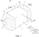
- a first direction may be defined as a direction in which first and second internal electrodes are alternately disposed with a dielectric layer interposed therebetween or a thickness (T) direction, and among second and third directions, perpendicular to the first direction, the second direction may be defined as a length (L) direction, and the third direction may be defined as a width (W) direction.
- FIG. 1 is a perspective view illustrating a multilayer electronic component according to an embodiment of the present disclosure.
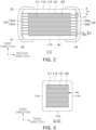
- FIG. 2 is a cross-sectional view taken along line I-I' of FIG. 1 .
- FIG. 3 is a cross-sectional view taken along line II-II' of FIG. 1 .
- FIG. 4 is an exploded perspective view illustrating a body of a multilayer electronic component according to an embodiment of the present disclosure.
- FIG. 5 is an enlarged view of region P1 of FIG. 2 .
- FIGS. 6 (a) and 6(b) are schematic diagrams schematically illustrating a method of measuring a growth direction of a first crystal grain and a growth direction of a second crystal grain according to an embodiment of the present disclosure.
- FIGS. 1 to 6(b) a multilayer electronic component 100 according to an embodiment of the present disclosure will be described with reference to FIGS. 1 to 6(b) .
- the multilayer electronic component 100 includes: a body 110 including a dielectric layer 111 and internal electrodes 121 and 122 alternately disposed with the dielectric layer 111 in a first direction, the body 110 having first and second surfaces 1 and 2 opposing each other in a first direction, third and fourth surfaces 3 and 4 connected to the first and second surfaces and opposing each other in a second direction, and fifth and sixth surfaces 5 and 6 connected to the first to fourth surfaces 1, 2, 3, and 4 and opposing each other in a third direction; first electrode layers 131a and 132a disposed on the third and fourth surfaces 3 and 4 and disposed on an extension line E1 of the first surface and an extension line E2 of the second surface, and second electrode layers 131b and 132b disposed on the first electrode layers 131a and 132a, wherein the first electrode layers 131a and 132a include first crystal grains G1 and G1' disposed on an end of the dielectric layer 111 in a second direction and in contact with the second electrode layers 131b and
- the body 110 has a dielectric layer 111 and internal electrodes 121 and 122, alternately stacked therein.
- the body 110 is not limited to a particular shape, and may have a hexahedral shape or a shape similar to the hexahedral shape, as illustrated in the drawings.
- the body 110 may not have the shape of a hexahedron having perfectly straight lines because ceramic powder particles included in the body 110 are contracted in a process in which the body is sintered.
- the body 110 may have a substantially hexahedral shape.
- the body 110 may have first and second surfaces 1 and 2 opposing each other in a first direction, third and fourth surfaces 3 and 4 connected to the first and second surfaces 1 and 2 and opposing each other in a second direction, and fifth and sixth surfaces 5 and 6 connected to the first and second surfaces 1 and 2, connected to the third and fourth surfaces 3 and 4, and opposing each other in a third direction.
- a plurality of dielectric layers 111 forming the body 110 may be in a sintered state, and adjacent dielectric layers 111 may be integrated with each other, such that boundaries therebetween may not be readily apparent without a scanning electron microscope (SEM).
- SEM scanning electron microscope
- a raw material for forming the dielectric layer 111 is not particularly limited, as long as sufficient electrostatic capacitance may be obtained therewith.
- the raw material for forming the dielectric layer 111 may be a barium titanate (BaTiO 3 )-based material, a lead composite perovskite-based material, a strontium titanate (SrTiO 3 )-based material, or the like.
- the barium titanate-based material may include BaTiO 3 -based ceramic powder, and the ceramic powder may be, for example, BaTiO 3 , (Ba 1-x Ca x )TiO 3 , Ba(Ti 1-y Ca y )O 3 , (Ba 1-x Ca x )(Ti 1-y Zr y )O 3 or Ba(Ti 1-y Zr y )O 3 , in which calcium (Ca), zirconium (Zr), or the like, are partially dissolved in BaTiO 3 , and the like.
- the ceramic powder may be, for example, BaTiO 3 , (Ba 1-x Ca x )TiO 3 , Ba(Ti 1-y Ca y )O 3 , (Ba 1-x Ca x )(Ti 1-y Zr y )O 3 or Ba(Ti 1-y Zr y )O 3 , in which calcium (Ca), zirconium (Zr), or the like, are partially
- a raw material of the dielectric layer 111 may include various ceramic additives, organic solvents, binders, dispersants, and the like, added to powder particles such as barium titanate (BaTiO 3 ) powder particles, or the like, according to an object of the present disclosure.
- various ceramic additives such as barium titanate (BaTiO 3 ) powder particles, or the like, according to an object of the present disclosure.
- an average thickness "td” of the dielectric layer 111 is not particularly limited.
- the average thickness "td” of the dielectric layer 111 may be 0.2 ⁇ m or more and 2 ⁇ m less.
- the dielectric layer is formed thinly to a thickness of less than 0.6 um, in particular, when the thickness of the dielectric layer is 0.35 um or less, reliability of the multilayer electronic component 100 may be further deteriorated.
- the present disclosure by adjusting an absolute value of a difference between an average value of a first angle ⁇ 1 and a second angle ⁇ 2, to be described later, even when the average thickness "td" of the dielectric layer 111 is 0.35 ⁇ m or less, reliability of the multilayer electronic component 100 may be secured. That is, when the average thickness "td" of the dielectric layer 111 is 0.35 um or less, a reliability improvement effect according to the present disclosure may be more remarkable.
- the average thickness "td" of the dielectric layer 111 may refer to an average thickness "td” of the dielectric layer 111 disposed between the first and second internal electrodes 121 and 122.
- the average thickness "td" of the dielectric layer 111 may be measured by scanning an image of a cross-section of the body 110 in length and thickness directions (L-T directions) with a scanning electron microscope (SEM) with a magnification of 10,000. More specifically, an average value may be measured by measuring a thickness of one dielectric layer at 30 equally spaced points in the length direction from the scanned image. The 30 points having equal intervals may be designated in the capacitance formation portion Ac. In addition, if the average value is measured by extending the average value measurement to 10 dielectric layers, the average thickness of the dielectric layers can be more generalized.
- the body 110 may include a capacitance formation portion Ac disposed inside the body 110 and including a first internal electrode 121 and a second internal electrode 122 alternately disposed with the dielectric layer 111 interposed therebetween to form capacitance and cover portions 112 and 113 formed above and below the capacitance formation portion Ac in a first direction.
- the capacitance formation portion Ac is a portion contributing to forming capacitance of the capacitor, may be formed by repeatedly stacking a plurality of first and second internal electrodes 121 and 122 with a dielectric layer 111 interposed therebetween.
- an upper cover portion 112 may be disposed on one surface of the capacitance formation portion Ac in a first direction, and a lower cover portion 113 may be disposed on the other surface of the capacitance formation portion Ac in the first direction.
- the upper cover portion 112 and the lower cover portion 113 may be formed by stacking a single dielectric layer or two or more dielectric layers on the upper and lower surfaces of the capacitance formation portion Ac in a thickness direction, respectively, and the upper cover portion 112 and the lower cover portion 113 may serve to basically prevent damage to the internal electrodes due to physical or chemical stress.
- the upper cover portion 112 and the lower cover portion 113 may not include internal electrodes, and may include the same material as that of the dielectric layer 111.
- the upper cover portion 112 and the lower cover portion 113 may include a ceramic material, for example, a barium titanate (BaTiO 3 )-based ceramic material.
- an average thickness of the cover portions 112 and 113 is not particularly limited. However, in order to more easily implement miniaturization and high capacitance of the multilayer electronic component, the average thickness "tc" of the cover portions 112 and 113 may be 15 ⁇ m or less. In addition, according to an embodiment of the present disclosure, by adjusting an absolute value of a difference between an average value of a first angle ⁇ 1 and an average value of a second angle ⁇ 2, to be described later, to 20 degrees or less, even when the average thickness "tc" of the cover portion is 15 um or less, the reliability of the multilayer electronic component 100 may be secured.
- the average thickness of the cover portions 112 and 113 may refer to a size thereof in the first direction, and may be a value obtained by averaging sizes of the cover portions 112 and 113 measured at five points having equal intervals in the first direction above or below the capacitance formation portion Ac.
- margin portions 114 and 115 may be disposed on a side surface of the capacitance formation portion Ac.
- the margin portions 114 and 115 may include a margin portion 114 disposed on the fifth surface 5 of the body 110 and a margin portion 115 disposed on the sixth surface 6 thereof. That is, the margin portions 114 and 115 may be disposed on both end surfaces of the body in a third direction (width direction).
- the margin portions 114 and 115 may refer to a region between both ends of the first and second internal electrodes 121 and 122 and an interface of the body 110, in a cross-section of the body 110 cut in width-thickness (W-T) directions, as illustrated in FIG. 3 .
- the margin portions 114 and 115 may basically serve to prevent damages to the internal electrodes due to physical or chemical stresses.
- the margin portions 114 and 115 may be formed by applying a conductive paste to a ceramic green sheet, except where margin portions are to be formed, to form internal electrodes.
- the margin portions 114 and 115 may also be formed by stacking a single dielectric layer or two or more dielectric layers on both side surfaces of the capacitance formation portion Ac in the third direction (width direction).
- a width of the margin portions 114 and 115 is not particularly limited. However, in order to more easily implement miniaturization and high capacitance of the multilayer electronic component, the average width of the margin portions 114 and 115 may be 15 ⁇ m or less. In addition, according to an embodiment of the present disclosure, by adjusting an absolute value of a difference between an average value of the first angle ⁇ 1 and an average value of the second angle ⁇ 2 to 20 degrees or less, even when an average width of the margin portions 114 and 115 is 15 um or less, the reliability of the multilayer electronic component 100 may be secured.
- the average width of the marginal portions 114 and 115 may refer to an average size of the marginal portions 114 and 115 in a third direction, and may be a value obtained by averaging sizes of the margin portions 114 and 115 measured at five points having equal intervals in the third direction on the side surface of the capacitance formation portion Ac.
- the internal electrodes 121 and 122 and the dielectric layer 111 are alternately disposed in a first direction.
- the internal electrodes 121 and 122 may include first and second internal electrodes 121 and 122.
- the first and second internal electrodes 121 and 122 may be alternately disposed to oppose each other with the dielectric layer 111 constituting the body 110 interposed therebetween, and may be respectively connected to the third and fourth surfaces 3 and 4 of the body 110.
- one end of the first internal electrode 121 may be connected to the third surface
- one end of the second internal electrode 122 may be connected to the fourth surface. That is, the internal electrodes 121 and 122 in an embodiment may be in contact with the third surface 3 or the fourth surface 4.
- the first internal electrode 121 may be spaced apart from the fourth surface 4 and exposed through the third surface 3, and the second internal electrode 122 may be spaced apart from the third surface 3 and exposed through the fourth surface 4.
- a first external electrode 131 may be disposed on the third surface 3 of the body and connected to the first internal electrode 121, and a second external electrode 132 may be disposed on the fourth surface 4 and connected to the second internal electrode 122.
- the first internal electrode 121 may be connected to the first external electrode 131 without being connected to the second external electrode 132, and the second internal electrode 122 may be connected to the second external electrode 132 without being connected to the first external electrode 132. Accordingly, the first internal electrode 121 may be formed to be spaced apart from the fourth surface 4 by a predetermined distance, and the second internal electrode 122 may be formed to be spaced apart from the third surface 3 by a predetermined distance.
- first and second internal electrodes 121 and 122 may be electrically isolated from each other by the dielectric layer 111 disposed in a middle.
- the body 110 may be formed by alternately stacking a ceramic green sheet on which the first internal electrode 121 is printed and a ceramic green sheet on which the second internal electrode 122 is printed, and then sintering the same.
- a material for forming internal electrodes 121 and 122 is not particularly limited, and a material having excellent electrical conductivity may be used.
- the internal electrodes 121 and 122 may include at least one of nickel (Ni), copper (Cu), palladium (Pd), silver (Ag), gold (Au), platinum (Pt), tin (Sn), or tungsten (W), titanium (Ti), and alloys thereof.
- the internal electrodes 121 and 122 may be formed by printing a conductive paste for internal electrodes including at least one of nickel (Ni), copper (Cu), palladium (Pd), silver (Ag), gold (Au), platinum (Pt), tin (Sn), tungsten (W), and alloys thereof, on a ceramic green sheet.
- a method of printing the conductive paste for internal electrodes may be a screen printing method, a gravure printing method, or the like, but the present disclosure is not limited thereto.
- an average thickness "te" of the internal electrodes 121 and 122 is not particularly limited.
- the average thickness "te” of the internal electrodes 121 and 122 may be 0.2 um or more and 2 ⁇ m less.
- the effect according to the present disclosure may be more remarkable, and miniaturization and high capacitance of the multilayer electronic component may be more easily achieved.
- the average thickness "te" of the internal electrodes 121 and 122 may refer to an average thickness "te” of the internal electrodes 121 and 122.
- the average thickness "te" of the internal electrodes 121 and 122 may be measured by scanning an image of a cross-section of the body 110 in length and thickness directions (L-T) with a scanning electron microscope (SEM) at a magnification of 10,000. More specifically, an average value may be measured by measuring a thickness of one of the internal electrodes at 30 equally spaced points in the length direction in the scanned image. The 30 equally spaced points may be designated in the capacitance formation portion Ac. In addition, if the average value is measured by extending the average value measurement to 10 internal electrodes, the average thickness of the internal electrodes can be more generalized.
- First electrode layers 131a and 132a disposed between an extension line E1 of the first surface and an extension line E2 of the second surface are disposed on the third and fourth surfaces 3 and 4 of the body 110.
- the first electrode layer is in contact with and electrically connected to the internal electrodes 121 and 122.
- the first electrode layer 131a is in contact with and electrically connected to the first internal electrode 121
- the first electrode layer 132a is in contact with and electrically connected to the second internal electrode 122.
- the first electrode layers 131a and 132a may include a conductive metal element, which may serve to secure connectivity with the internal electrodes 121 and 122.
- the type of conductive metal element is not particularly limited, and the first electrode layers 131a and 132a may include at least one of Cu, Ni, Pd, Cr, and alloys thereof, and first crystal grains G1 and G1' and second crystal grains G2 and G2' to be described later may include at least one of Cu, Ni, Pd, Cr, and alloys thereof.
- crystal grains disposed on an end of the dielectric layer 111 in a second direction and in contact with the second electrode layers 131b and 132b may be defined as first crystal grains G1 and G1' and crystal grains disposed on ends of the internal electrodes 121 and 122 in the second direction and in contact with the second electrode layers 131b and 132b may be defined as second crystal grains G2 and G2', and a growth direction V1 of the first crystal grains G1 and G1' and a growth direction V2 of the second crystal grains G2 and G2' may be adjusted so that bonding force between the first electrode layers 131a and 132a may be improved.
- an absolute value of a difference between the average value of the first angle ⁇ 1 and the average value of the second angle ⁇ 2 is 20 degrees or less.
- first and second crystal grains G1, G1', G2, and G2', growth directions V1 and V2 of the first and second crystal grains, and first and second angles ⁇ 1 and ⁇ 2 will be described in detail with reference to the second internal electrode 122, the first electrode layer 132a, and the second electrode layer 132b. This description can be similarly applied with reference to the first internal electrode 122, the first electrode layer 131a, and the second electrode layer 131b.
- a method of measuring the growth directions V1, V1', V2, and V2' of the first and second crystal grains and the first and second angles ⁇ 1 and ⁇ 2 is not particularly limited.
- growth directions V1, V1', V2, and V2' of first and second crystal grains and first and second angles ⁇ 1 and ⁇ 2 were measured by processing a region of 20 um ⁇ 20 um or more with a focused ion beam (FIB) based on a surface in which an internal electrode disposed at the top or bottom of the internal electrodes 121 and 122 in the first direction and first and second electrode layers 131a and 132a are in contact with each other, and then performing scanning electron microscope (SEM) analysis thereon.
- FIB focused ion beam
- FIG. 5 is an enlarged view of the P1 region of FIG. 2
- FIGS. 6 (a) and 6 (b) are schematic diagrams schematically illustrating a method of measuring a growth direction of a first crystal grain and a growth direction of a second crystal grain according to an embodiment of the present disclosure.
- the first electrode layers 131a and 132a may include a plurality of crystal grains.
- the plurality of crystal grains may have a form in which grain growth progresses from the fourth surface 4 of the body toward the second electrode layer 132b. Accordingly, among the plurality of crystal grains, sizes of crystal grains in contact with the second electrode layers 131b and 132b may be greater than sizes thereof in contact with the fourth surface 4, and in an embodiment, the sizes of the plurality of crystal sizes may gradually increase from the fourth surface 4 to the second electrode layers 131b and 132b.
- crystal grains in contact with the second electrode layers 131b and 132b are defined as first and second crystal grains G1, G1', G2, and G2'.
- first and second crystal grains G1, G1', G2, and G2' crystal grains disposed on an end of the dielectric layer 111 in a second direction are defined as first crystal grains G1 and G1', and crystal grains disposed on an end of the internal electrode 122 in the second direction are defined as second crystal grains G2 and G2'.
- crystal grains simultaneously disposed on the end of the dielectric layer 111 in the second direction and the end of the internal electrode 122 in the second direction are defined as second crystal grains G2 and G2'.
- the growth directions V1 and V2 of the first and second crystal grains G1 and G2 may refer to, in the first and second crystal grains G1 and G2, a direction of a straight line connecting a midpoint M1 of an uppermost line segment in a second direction, in contact with the second electrode layer 132b and a midpoint M2 of a lowermost line segment in the second direction, in contact with the second electrode layer 132b.
- the first and second crystal grains G1' and G2' may have a sharp point located at the bottom according to grain growth conditions.
- the "growth directions V1 and V2 of the first and second crystal grains” may refer to, in the first and second crystal grains G1' and G2', a direction of a straight line connecting a midpoint M1 of an uppermost line segment in the second direction in contact with the second electrode layer 132b and lowermost sharp points SP1 and SP2 thereof.
- an angle formed by the growth direction V1 of the first crystal grain and extension lines E3 and E4 of the third or fourth surface is defined as a first angle ⁇ 1
- an angle formed by the growth direction V2 of the second crystal grain V2 and the extension lines E3 and E4 of the third surface or fourth surface is defined as a second angle ⁇ 2.
- an absolute value of a difference between an average value of the first angle ⁇ 1 and an average value of the second angle ⁇ 2 is preferably 20 degrees or less.
- the average value of the first angle ⁇ 1 may refer to an average value of the first angle ⁇ 1 values measured from five or more of the arbitrary first crystal grains G1 and G1'
- the average value of the second angle ⁇ 2 may refer to an average value of second angle values ⁇ 2 measured from five or more of the arbitrary second crystal grains G2 and G2'.
- the average value of the first angle ⁇ 1 and the average value of the second angle ⁇ 2 can be further generalized by measuring in five or more arbitrary regions equally spaced in the first direction from the P1 region, and the arbitrary five or more regions equally spaced from the P1 region in the first direction may have substantially the same area as the P1 region, and substantially the same pre-treatment may be performed.
- a method of adjusting the average value of the first angle ⁇ 1 and the average value of the second angle ⁇ 2 is not particularly limited.
- the end of the dielectric layer 111 in the second direction may be selectively reduced through a high-power laser on the third and fourth surfaces 3 and 4 of the body 110 and an electrolytic plating method or an electroless plating method may be used on the third and fourth surfaces 3 and 4 thereof, so that first electrode layers 131a and 132a may be formed.
- the average value of the first angle ⁇ 1 and the average value of the second angle ⁇ 2 may be adjusted.
- the high temperature and moisture resistance reliability of the multilayer electronic component 100 may be improved by improving the bonding force between the end of the dielectric layer 111 in the second direction and the first electrode layers 131a and 132a.
- the growth direction V1 of the first crystal grain and the growth direction V2 of the second crystal grain may be substantially the same. Accordingly, by minimizing a difference in crystal growth directions between the crystal grains of the first electrode layer disposed on the end of the dielectric layer 111 in the second direction and the crystal grains of the second electrode layer disposed on the ends of the internal electrodes 121 and 122 in the second direction, high temperature and moisture resistance reliability of the multilayer electronic component 100 may be further improved.
- the fact that the growth direction V1 of the first crystal grain and the crystal growth direction V2 of the second crystal grain are substantially the same refers to that an absolute value of the difference between the average value of the first angle ⁇ 1 and the average value of the second angle ⁇ 2 is 15 degrees or less.
- a method of forming the first electrode layers 131a and 132a is not particularly limited, but preferably, thin and dense first electrode layers 131a and 132a may be formed on the third and fourth surfaces 3 and 4 of the body 110 using an electroplating or electroless plating method. That is, in an embodiment, the first electrode layers 131a and 132a may not include glass. When glass is not included in the first electrode layers 131a and 132a, on the third and fourth surfaces 3 and 4, the end of the dielectric layer 111 in the second direction and the first electrode layers 131a and 132a may have a problem in that bonding strength is deteriorated due to a difference in components.
- the bonding force between the first electrode layers 131a and 132a and the body is improved by adjusting the growth direction V1 of the first crystal grain and the growth direction V2 of the second crystal grain as in an embodiment of the present disclosure, even when the first electrode layers 131a and 132a do not include glass, the bonding force between the body 110 and the first electrode layers 131a and 132a can be sufficiently improved.
- Second electrode layers 131b and 132b are disposed on the first electrode layers 131a and 132a.
- the second electrode layers 131b and 132b may serve to secure plating properties and mountability, and may serve to protect the multilayer electronic component 100 from external impact.
- the second electrode layers 131b and 132b may include glass and may further include at least one of Cu, Ni, Ag, Sn, Cr, Pd, and alloys thereof. Accordingly, by forming a plating layer on the second electrode layers 131b and 132b, oxidation of the first electrode layers 131a and 132a can be prevented and mountability can be secured.
- the second electrode layers 131b and 132b may be disposed to extend from the first electrode layers 131a and 132a to a portion of at least one of the first, second, fifth, and sixth surfaces 1, 2, 5, and 6 of the body 110. Accordingly, a sufficient mounting area can be secured.
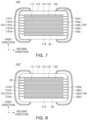
- FIG. 7 is cross-sectional view of a multilayer electronic component 100' in first and second directions according to an embodiment.
- protective layers 131c and 132c may be disposed on the third and fourth surfaces not covered by the first and second electrode layers 131a and 132a and an interface of the second electrode layers 131b and 132b.
- the protective layers 131c and 132c may include glass, and the glass included in the protective layers 131c and 132c may be one in which the glass included in the second electrode layers 131b and 132b move to the third and fourth surfaces and the interface of the second electrode layers 131b and 132b.
- the protective layers 131c and 132c may be formed on third and fourth surfaces on which the internal electrodes 121 and 122 are not disposed, and may be formed on an interface in which the cover portions 112 and 113 and the margin portions 114 and 115 are in contact with the second electrode layers 131b and 132b.
- the content of the glass included in the second electrode layers 131b and 132b may gradually decrease from the interface between the body 110 and the second electrode layers 131b and 132b to outer surfaces of the second electrode layers 131b and 132b.
- FIG. 8 is cross-sectional view of a multilayer electronic component 100" in first and second directions according to an embodiment
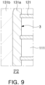
- FIG. 9 is an enlarged view of a region P2 of FIG. 8 .
- the multilayer electronic component 100" may have a shape protruding from the third and fourth surfaces 3 and 4 of the body in a second direction. Accordingly, by improving a contact area between the first electrode layers 131a and 132a and ends of the internal electrodes 121 and 122 in the second direction, and further improving the bonding force between the first electrode layers 131a and 132a and the body 110, high temperature and moisture resistance reliability of the multilayer electronic component 100" can be further improved.
- the first electrode layers 131a and 132a are disposed to cover the protruding ends of the internal electrodes, an effect of improving high-temperature and moisture resistance reliability may be more remarkable.
- the protruding shape of the first internal electrode 121 is expressed with respect to the third surface 3, but the protruding shape of the second internal electrode 122 with respect to the fourth surface 4 may also be understood in the same manner.
- the first electrode layers 131a and 132a and the second electrode layers 131b and 132b described above may constitute external electrodes 131 and 132.
- the first electrode layers 131a and 132a, the second electrode layers 131b and 132b, and the protective layers 131c and 132c may also constitute external electrodes 131' and 132'.
- the protective layers 131c and 132c may not be essential components of the present disclosure, and it should be noted that it does not mean the external electrodes 131 and 132 include only the first electrode layers 131a and 132a and the second electrode layers 131b and 132b.
- the external electrodes 131 and 132 may include plating layers on the second electrode layers 131b and 132b, and the plating layer serves to improve mounting properties.
- the type of the plating layer is not particularly limited, and may be a plating layer including at least one of Ni, Sn, Pd, and alloys thereof, and may be formed of a plurality of layers.
- the plating layer may be a Ni plating layer or a Sn plating layer, may have a form in which a Ni plating layer and a Sn plating layer are sequentially formed on the electrode layer, and have a form in which a Sn plating layer, a Ni plating layer, and a Sn plating layer are sequentially formed.
- the plating layer may include a plurality of Ni plating layers and/or a plurality of Sn plating layers.
- the second electrode layers 131b and 132b may include conductive metal and a resin. Accordingly, the multilayer electronic component 100 can be protected from stress caused by warpage of an external substrate or stress caused by solder reflow.
- the type of the resin is not particularly limited, and may be a resin having ductility and strong heat resistance.
- the resin may be a phenolic resin, urea resin, diallylphthalate resin, melanin resin, guanamine resin, unsaturated polyester resin, polyurethane resin, epoxy resin, acrylic resin, ethyl cellulose resin, aminoalkyd resin, melamine-urea copolymer resin, silicon resin, polysiloxane resin, and the like, but an embodiment thereof is not limited thereto.
- a curing agent such as a crosslinking agent, a polymerization initiator, and the like, may be further added as needed.
- the multilayer electronic component 100 has two external electrodes 131 and 132 is described, but the number and shape of the external electrodes 131 and 132 may be changed according to the shape of the internal electrodes 121 and 122 or other purposes.
- a size of the multilayer electronic component 100 is not particularly limited.
- the thickness of the dielectric layer and internal electrodes should be thinned to increase the number of stacked layers thereof, so that an adhesion strength improvement effect according to the present disclosure may be more remarkable in the multilayer electronic component 100 having a size of 0603 (length X width, 0.6 mm X 0.3 mm) or less.
- a length of the multilayer electronic component 100 may refer to a maximum size of the multilayer electronic component 100 in the second direction
- a width of the multilayer electronic component 100 may refer to a maximum size of the multilayer electronic component 100 in the third direction.
- Table 1 shows results of evaluation of high-temperature reliability and moisture resistance reliability according to an absolute value of a difference between an average value ⁇ 1 of a first angle ⁇ 1 and an average value ⁇ 2 of a second angle ⁇ 2 according to an embodiment of the present disclosure.
- the average value ⁇ 1 of the first angle ⁇ 1 and the average value ⁇ 2 of the second angle ⁇ 2 were adjusted by changing a condition for selectively reducing an end of the dielectric layer 111 in a second direction, and other than that, conditions were equally applied to all samples.
- growth directions V1, V1', V2, and V2' of first and second crystal grains and first and second angles ⁇ 1 and ⁇ 2 were measured by processing a region of 20 um ⁇ 20 um or more with a focused ion beam (FIB) based on a surface in which an internal electrode disposed at the top or bottom of the internal electrodes 121 and 122 in the first direction and first and second electrode layers 131a and 132a are in contact with each other, and then performing scanning electron microscope (SEM) analysis thereon.
- FIB focused ion beam
- first and second crystal grains G1 and G2 a direction of a straight line connecting a midpoint M1 of an uppermost line segment and a midpoint M2 of a lowermost line segment, in contact with the second electrode layer 132b, was measured as the growth directions V1 and V2 of the first and second crystal grains.
- first and second crystal grains G1' and G2' may have a sharp point located at the bottom according to grain growth conditions.
- a direction of a straight line connecting the midpoint M1 of the uppermost lone segment in the second direction, contacting the second electrode layer 132b and the lowermost sharp points SP1 and SP2 was measured as crystal growth directions V1 and V2 of the first and second crystal grains.
- an angle formed by the growth direction V1 of the first crystal grain and extension lines E3 and E4 of the third surface or the fourth surface was measured as a first angle ⁇ 1
- an angle formed by the growth direction V2 of the second crystal grain and extension lines E3 and E4 of the third surface or the fourth surface was measured as a second angle ⁇ 2.
- an average value ( ⁇ 1 ) of the first angle ⁇ 1 was taken from a value of the first angle ⁇ 1, measured from five or more crystal grains among random first crystal grains G1 and G1'
- an average value ( ⁇ 2 ) of the second angle ⁇ 2 was taken from a value of the first angle ⁇ 1, measured from five or more crystal grains among random first crystal grains G2 and G2'.
- High-temperature reliability evaluation was conducted for 12 hours at 105 ° C and 1 Vr, and moisture resistance evaluation was conducted for 24 hours at 95 ° C, 95% relative humidity and 0.6 Vr, and the high-temperature reliability evaluation and the moisture resistance evaluation were conducted with 1200 samples for each test number.
- IR insulation resistance
- Test Nos. 1 and 2 are cases in which a value of
- Test Nos. 3 and 4 are cases in which a value of
- ) of the difference between the average value of the first angle and the average value of the second angle may be 20 degrees or less. Therefore, in an embodiment of the present disclosure, by adjusting the absolute value (
- a first electrode layer including crystal grains is formed on third and fourth surfaces of the body, by adjusting an angle formed by a growth direction of the crystal grains and extension lines of the third and fourth surfaces, to improve bonding force between the first electrode layer and the body, moisture resistance and high-temperature reliability of the multilayer electronic component may be improved.
Landscapes
- Engineering & Computer Science (AREA)
- Power Engineering (AREA)
- Manufacturing & Machinery (AREA)
- Microelectronics & Electronic Packaging (AREA)
- Chemical & Material Sciences (AREA)
- Ceramic Engineering (AREA)
- Inorganic Chemistry (AREA)
- Materials Engineering (AREA)
- Fixed Capacitors And Capacitor Manufacturing Machines (AREA)
- Ceramic Capacitors (AREA)
Abstract

Description
- This application claims benefit of priority to
Korean Patent Application No. 10-2022-0164541 filed on November 30, 2022 - The present disclosure relates to a multilayer electronic component.
- A multilayer ceramic capacitor (MLCC), a multilayer electronic component, may be a chip-type condenser mounted on the printed circuit boards of any of various types of electronic products, such as an image display device, including a liquid crystal display (LCD) or a plasma display panel (PDP), a computer, a smartphone, or a mobile phone, serving to charge or discharge electricity therein or therefrom.
- In general, an external electrode of a multilayer ceramic capacitor may include a conductive metal and glass. Accordingly, bonding force between a ceramic component of a capacitor body and internal electrodes may be secured. When external electrodes, internal electrodes, and dielectric layers are formed thinly for miniaturization and high capacitance of the multilayer ceramic capacitor, the bonding force between the external electrodes and the body may deteriorate due to the lack of absolute glass content in the external electrodes, and the density of the external electrodes may decrease. Thus, a permeation path of external moisture or plating solution may be formed. In order to solve this problem, when a glass content of the external electrode is increased, a problem of deterioration in contact and connectivity between the conductive metal of the external electrode and the internal electrodes may occur.
- In order to improve this, an attempt has been made to secure connectivity between the internal electrode and the external electrode by directly forming external electrodes on a surface of a body using a plating method after sintering the body of the capacitor. However, due to the characteristics of the plating method, the bonding force between the body and the external electrode is still insufficient due to the weak bonding force with a nonconductive dielectric layer.
- An aspect of the present disclosure is to solve a problem of deterioration in bonding force between a first electrode layer and a body, which may occur as a growth direction of crystal grains is different on an end of a dielectric layer and on ends of internal electrodes, when a first electrode layer including the crystal grains on third and fourth surfaces of the body.
- However, the object of the present disclosure is not limited to the above, and will be more easily understood in the process of describing specific embodiments of the present disclosure.
- According to an aspect of the present disclosure, a multilayer electronic component includes: a body including a dielectric layer and internal electrodes alternately disposed with the dielectric layer interposed therebetween in a first direction, the body having first and second surfaces opposing each other in the first direction, third and fourth surfaces connected to the first and second surfaces and opposing each other in a second direction, and fifth and sixth surfaces connected to the first to fourth surfaces and opposing each other in a third direction; a first electrode layer disposed on the third and fourth surfaces and disposed between an extension line of the first surface and an extension line of the second surface; and a second electrode layer disposed on the first electrode layer, wherein the first electrode layer includes a first crystal grain disposed on an end of the dielectric layer in the second direction and in contact with the second electrode layer, and a second crystal grain disposed on ends of the internal electrodes in the second direction and in contact with the second electrode layer, wherein, when an angle formed by a growth direction of the first crystal grain and an extension line of the third surface or the fourth surface is referred to as a first angle, and an angle formed by a growth direction of the second crystal grain and an extension line of the third surface or the fourth surface is referred to as a second angle, and an absolute value of a difference between an average value of the first angle and an average value of the second angle is 20 degrees or less.
- The above and other aspects, features, and advantages of the present disclosure will be more clearly understood from the following detailed description, taken in conjunction with the accompanying drawings:
-
FIG. 1 is a perspective view illustrating a multilayer electronic component according to an embodiment of the present disclosure; -
FIG. 2 is a cross-sectional view taken along line I-I' ofFIG. 1 ; -
FIG. 3 is a cross-sectional view taken along line II-II' ofFIG. 1 ; -
FIG. 4 is an exploded perspective view illustrating a body of a multilayer electronic component according to an embodiment of the present disclosure; -
FIG. 5 is an enlarged view of region P1 ofFIG. 2 ; -
FIGS. 6 (a) and 6(b) are schematic diagrams schematically illustrating a method of measuring a growth direction of a first crystal grain and a growth direction of a second crystal grain according to an embodiment of the present disclosure; -
FIG. 7 is a cross-sectional view of a multilayer electronic component in first and second directions according to an embodiment; -
FIG. 8 is a cross-sectional view of a multilayer electronic component in first and second directions according to an embodiment; and -
FIG. 9 is an enlarged view of region P2 ofFIG. 8 . - Hereinafter, embodiments of the present disclosure will be described as follows with reference to the attached drawings. The present disclosure may, however, be exemplified in many different forms and should not be construed as being limited to the specific embodiments set forth herein. Rather, these embodiments are provided so that this disclosure will be thorough and complete, and will fully convey the scope of the disclosure to those skilled in the art. Accordingly, shapes and sizes of elements in the drawings may be exaggerated for clear description, and elements indicated by the same reference numeral are the same elements in the drawings.
- In the drawings, irrelevant descriptions will be omitted to clearly describe the present disclosure, and to clearly express a plurality of layers and areas, thicknesses may be magnified. The same elements having the same function within the scope of the same concept will be described with use of the same reference numerals. Throughout the specification, when a component is referred to as "comprise" or "comprising," it means that it may further include other components as well, rather than excluding other components, unless specifically stated otherwise.
- In the drawings, a first direction may be defined as a direction in which first and second internal electrodes are alternately disposed with a dielectric layer interposed therebetween or a thickness (T) direction, and among second and third directions, perpendicular to the first direction, the second direction may be defined as a length (L) direction, and the third direction may be defined as a width (W) direction.
-
FIG. 1 is a perspective view illustrating a multilayer electronic component according to an embodiment of the present disclosure. -
FIG. 2 is a cross-sectional view taken along line I-I' ofFIG. 1 . -
FIG. 3 is a cross-sectional view taken along line II-II' ofFIG. 1 . -
FIG. 4 is an exploded perspective view illustrating a body of a multilayer electronic component according to an embodiment of the present disclosure. -
FIG. 5 is an enlarged view of region P1 ofFIG. 2 . -
FIGS. 6 (a) and 6(b) are schematic diagrams schematically illustrating a method of measuring a growth direction of a first crystal grain and a growth direction of a second crystal grain according to an embodiment of the present disclosure. - Hereinafter, a multilayer
electronic component 100 according to an embodiment of the present disclosure will be described with reference toFIGS. 1 to 6(b) . - The multilayer
electronic component 100 according to an embodiment of the present disclosure includes: abody 110 including adielectric layer 111 andinternal electrodes dielectric layer 111 in a first direction, thebody 110 having first andsecond surfaces fourth surfaces sixth surfaces fourth surfaces first electrode layers fourth surfaces second electrode layers first electrode layers first electrode layers dielectric layer 111 in a second direction and in contact with thesecond electrode layers internal electrodes second electrode layers - The
body 110 has adielectric layer 111 andinternal electrodes - The
body 110 is not limited to a particular shape, and may have a hexahedral shape or a shape similar to the hexahedral shape, as illustrated in the drawings. Thebody 110 may not have the shape of a hexahedron having perfectly straight lines because ceramic powder particles included in thebody 110 are contracted in a process in which the body is sintered. However, thebody 110 may have a substantially hexahedral shape. - The
body 110 may have first andsecond surfaces fourth surfaces second surfaces sixth surfaces second surfaces fourth surfaces - A plurality of
dielectric layers 111 forming thebody 110 may be in a sintered state, and adjacentdielectric layers 111 may be integrated with each other, such that boundaries therebetween may not be readily apparent without a scanning electron microscope (SEM). - According to an embodiment of the present disclosure, a raw material for forming the
dielectric layer 111 is not particularly limited, as long as sufficient electrostatic capacitance may be obtained therewith. For example, the raw material for forming thedielectric layer 111 may be a barium titanate (BaTiO3)-based material, a lead composite perovskite-based material, a strontium titanate (SrTiO3)-based material, or the like. The barium titanate-based material may include BaTiO3-based ceramic powder, and the ceramic powder may be, for example, BaTiO3, (Ba1-xCax)TiO3, Ba(Ti1-yCay)O3, (Ba1-xCax)(Ti1-yZry)O3 or Ba(Ti1-yZry)O3, in which calcium (Ca), zirconium (Zr), or the like, are partially dissolved in BaTiO3, and the like. - In addition, a raw material of the
dielectric layer 111 may include various ceramic additives, organic solvents, binders, dispersants, and the like, added to powder particles such as barium titanate (BaTiO3) powder particles, or the like, according to an object of the present disclosure. - Meanwhile, an average thickness "td" of the
dielectric layer 111 is not particularly limited. For example, the average thickness "td" of thedielectric layer 111 may be 0.2 µm or more and 2 µm less. However, in general, when the dielectric layer is formed thinly to a thickness of less than 0.6 um, in particular, when the thickness of the dielectric layer is 0.35 um or less, reliability of the multilayerelectronic component 100 may be further deteriorated. - According to an embodiment of the present disclosure, by adjusting an absolute value of a difference between an average value of a first angle Θ1 and a second angle Θ2, to be described later, even when the average thickness "td" of the
dielectric layer 111 is 0.35 µm or less, reliability of the multilayerelectronic component 100 may be secured. That is, when the average thickness "td" of thedielectric layer 111 is 0.35 um or less, a reliability improvement effect according to the present disclosure may be more remarkable. - The average thickness "td" of the
dielectric layer 111 may refer to an average thickness "td" of thedielectric layer 111 disposed between the first and secondinternal electrodes - The average thickness "td" of the
dielectric layer 111 may be measured by scanning an image of a cross-section of thebody 110 in length and thickness directions (L-T directions) with a scanning electron microscope (SEM) with a magnification of 10,000. More specifically, an average value may be measured by measuring a thickness of one dielectric layer at 30 equally spaced points in the length direction from the scanned image. The 30 points having equal intervals may be designated in the capacitance formation portion Ac. In addition, if the average value is measured by extending the average value measurement to 10 dielectric layers, the average thickness of the dielectric layers can be more generalized. - The
body 110 may include a capacitance formation portion Ac disposed inside thebody 110 and including a firstinternal electrode 121 and a secondinternal electrode 122 alternately disposed with thedielectric layer 111 interposed therebetween to form capacitance and coverportions - In addition, the capacitance formation portion Ac is a portion contributing to forming capacitance of the capacitor, may be formed by repeatedly stacking a plurality of first and second
internal electrodes dielectric layer 111 interposed therebetween. - In an embodiment, an
upper cover portion 112 may be disposed on one surface of the capacitance formation portion Ac in a first direction, and alower cover portion 113 may be disposed on the other surface of the capacitance formation portion Ac in the first direction. - The
upper cover portion 112 and thelower cover portion 113 may be formed by stacking a single dielectric layer or two or more dielectric layers on the upper and lower surfaces of the capacitance formation portion Ac in a thickness direction, respectively, and theupper cover portion 112 and thelower cover portion 113 may serve to basically prevent damage to the internal electrodes due to physical or chemical stress. - The
upper cover portion 112 and thelower cover portion 113 may not include internal electrodes, and may include the same material as that of thedielectric layer 111. - That is, the
upper cover portion 112 and thelower cover portion 113 may include a ceramic material, for example, a barium titanate (BaTiO3)-based ceramic material. - Meanwhile, an average thickness of the
cover portions cover portions electronic component 100 may be secured. - The average thickness of the
cover portions cover portions - In an embodiment,
margin portions - Referring to
FIG. 2 , themargin portions margin portion 114 disposed on thefifth surface 5 of thebody 110 and amargin portion 115 disposed on thesixth surface 6 thereof. That is, themargin portions - The
margin portions internal electrodes body 110, in a cross-section of thebody 110 cut in width-thickness (W-T) directions, as illustrated inFIG. 3 . - The
margin portions - The
margin portions - In addition, in order to suppress a step by the
internal electrodes sixth surfaces margin portions - Meanwhile, a width of the
margin portions margin portions margin portions electronic component 100 may be secured. - The average width of the
marginal portions marginal portions margin portions - The
internal electrodes dielectric layer 111 are alternately disposed in a first direction. - The
internal electrodes internal electrodes internal electrodes dielectric layer 111 constituting thebody 110 interposed therebetween, and may be respectively connected to the third andfourth surfaces body 110. Specifically, one end of the firstinternal electrode 121 may be connected to the third surface, and one end of the secondinternal electrode 122 may be connected to the fourth surface. That is, theinternal electrodes third surface 3 or thefourth surface 4. - The first
internal electrode 121 may be spaced apart from thefourth surface 4 and exposed through thethird surface 3, and the secondinternal electrode 122 may be spaced apart from thethird surface 3 and exposed through thefourth surface 4. A firstexternal electrode 131 may be disposed on thethird surface 3 of the body and connected to the firstinternal electrode 121, and a secondexternal electrode 132 may be disposed on thefourth surface 4 and connected to the secondinternal electrode 122. - That is, the first
internal electrode 121 may be connected to the firstexternal electrode 131 without being connected to the secondexternal electrode 132, and the secondinternal electrode 122 may be connected to the secondexternal electrode 132 without being connected to the firstexternal electrode 132. Accordingly, the firstinternal electrode 121 may be formed to be spaced apart from thefourth surface 4 by a predetermined distance, and the secondinternal electrode 122 may be formed to be spaced apart from thethird surface 3 by a predetermined distance. - In this case, the first and second
internal electrodes dielectric layer 111 disposed in a middle. - The
body 110 may be formed by alternately stacking a ceramic green sheet on which the firstinternal electrode 121 is printed and a ceramic green sheet on which the secondinternal electrode 122 is printed, and then sintering the same. - A material for forming
internal electrodes internal electrodes - In addition, the
internal electrodes - In addition, an average thickness "te" of the
internal electrodes internal electrodes - However, in general, when internal electrodes are formed thinly to a thickness of less than 0.6 um, and particularly when the thickness of internal electrodes is 0.35 um or less, reliability of the multilayer
electronic component 100 may be more problematic. - According to an embodiment of the present disclosure, by adjusting an absolute value of a difference between an average value of a first angle Θ1 and an average value of a second angle Θ2 to be described later, to 20 degrees or less, even when the average thickness "te" of the
internal electrodes - Therefore, when the average thickness of the
internal electrodes - The average thickness "te" of the
internal electrodes internal electrodes - The average thickness "te" of the
internal electrodes body 110 in length and thickness directions (L-T) with a scanning electron microscope (SEM) at a magnification of 10,000. More specifically, an average value may be measured by measuring a thickness of one of the internal electrodes at 30 equally spaced points in the length direction in the scanned image. The 30 equally spaced points may be designated in the capacitance formation portion Ac. In addition, if the average value is measured by extending the average value measurement to 10 internal electrodes, the average thickness of the internal electrodes can be more generalized. -
First electrode layers fourth surfaces body 110. The first electrode layer is in contact with and electrically connected to theinternal electrodes first electrode layer 131a is in contact with and electrically connected to the firstinternal electrode 121, and thefirst electrode layer 132a is in contact with and electrically connected to the secondinternal electrode 122. - The
first electrode layers internal electrodes first electrode layers - In an embodiment of the present disclosure, among a plurality of crystal grains included in the
first electrode layers dielectric layer 111 in a second direction and in contact with the second electrode layers 131b and 132b may be defined as first crystal grains G1 and G1' and crystal grains disposed on ends of theinternal electrodes first electrode layers - Hereinafter, the first and second crystal grains G1, G1', G2, and G2', growth directions V1 and V2 of the first and second crystal grains, and first and second angles Θ1 and Θ2 will be described in detail with reference to the second
internal electrode 122, thefirst electrode layer 132a, and thesecond electrode layer 132b. This description can be similarly applied with reference to the firstinternal electrode 122, thefirst electrode layer 131a, and thesecond electrode layer 131b. - A method of measuring the growth directions V1, V1', V2, and V2' of the first and second crystal grains and the first and second angles Θ1 and θ2 is not particularly limited. For example, in a cross-section of the multilayer
electronic component 100 in first and second directions, cut from a central portion thereof in a third direction, growth directions V1, V1', V2, and V2' of first and second crystal grains and first and second angles Θ1 and Θ2 were measured by processing a region of 20 um × 20 um or more with a focused ion beam (FIB) based on a surface in which an internal electrode disposed at the top or bottom of theinternal electrodes second electrode layers -
FIG. 5 is an enlarged view of the P1 region ofFIG. 2 , andFIGS. 6 (a) and 6 (b) are schematic diagrams schematically illustrating a method of measuring a growth direction of a first crystal grain and a growth direction of a second crystal grain according to an embodiment of the present disclosure. - Referring to
FIG. 5 , thefirst electrode layers fourth surface 4 of the body toward thesecond electrode layer 132b. Accordingly, among the plurality of crystal grains, sizes of crystal grains in contact with the second electrode layers 131b and 132b may be greater than sizes thereof in contact with thefourth surface 4, and in an embodiment, the sizes of the plurality of crystal sizes may gradually increase from thefourth surface 4 to the second electrode layers 131b and 132b. - In an embodiment of the present disclosure, among a plurality of crystal grains included in the
first electrode layers dielectric layer 111 in a second direction are defined as first crystal grains G1 and G1', and crystal grains disposed on an end of theinternal electrode 122 in the second direction are defined as second crystal grains G2 and G2'. In this case, crystal grains simultaneously disposed on the end of thedielectric layer 111 in the second direction and the end of theinternal electrode 122 in the second direction are defined as second crystal grains G2 and G2'. - Referring to
FIGS. 6(a) and 6(b) , in an embodiment of the present disclosure, "the growth directions V1 and V2 of the first and second crystal grains G1 and G2" may refer to, in the first and second crystal grains G1 and G2, a direction of a straight line connecting a midpoint M1 of an uppermost line segment in a second direction, in contact with thesecond electrode layer 132b and a midpoint M2 of a lowermost line segment in the second direction, in contact with thesecond electrode layer 132b. Meanwhile, the first and second crystal grains G1' and G2' may have a sharp point located at the bottom according to grain growth conditions. In this case, the "growth directions V1 and V2 of the first and second crystal grains" may refer to, in the first and second crystal grains G1' and G2', a direction of a straight line connecting a midpoint M1 of an uppermost line segment in the second direction in contact with thesecond electrode layer 132b and lowermost sharp points SP1 and SP2 thereof. - According to an embodiment of the present disclosure, an angle formed by the growth direction V1 of the first crystal grain and extension lines E3 and E4 of the third or fourth surface is defined as a first angle Θ1, and an angle formed by the growth direction V2 of the second crystal grain V2 and the extension lines E3 and E4 of the third surface or fourth surface is defined as a second angle Θ2. According to an embodiment of the present disclosure, an absolute value of a difference between an average value of the first angle Θ1 and an average value of the second angle Θ2 is preferably 20 degrees or less. Through this, bonding force between the end of the
dielectric layer 111 in the second direction and thefirst electrode layers electronic component 100 may be improved. - The average value of the first angle Θ1 may refer to an average value of the first angle Θ1 values measured from five or more of the arbitrary first crystal grains G1 and G1', and the average value of the second angle Θ2 may refer to an average value of second angle values Θ2 measured from five or more of the arbitrary second crystal grains G2 and G2'. The average value of the first angle Θ1 and the average value of the second angle Θ2 can be further generalized by measuring in five or more arbitrary regions equally spaced in the first direction from the P1 region, and the arbitrary five or more regions equally spaced from the P1 region in the first direction may have substantially the same area as the P1 region, and substantially the same pre-treatment may be performed.
- A method of adjusting the average value of the first angle Θ1 and the average value of the second angle Θ2 is not particularly limited. In an embodiment, the end of the
dielectric layer 111 in the second direction may be selectively reduced through a high-power laser on the third andfourth surfaces body 110 and an electrolytic plating method or an electroless plating method may be used on the third andfourth surfaces first electrode layers - In the conventional case of forming a first electrode layer using an electrolytic plating method or an electroless plating method on the third and
fourth surfaces dielectric layer 111 in the second direction, grain growth of conductive metal does not occur smoothly at the end of thedielectric layer 111 in the second direction, which has a ceramic raw material as a main component thereof, so that a large difference may occur in the growth directions of the crystal grains of the first electrode layer disposed on the end of thedielectric layer 111 in the second direction and the crystal grains of the second electrode layer disposed on the ends of theinternal electrodes body 110 and the first electrode layer may not be improved, and thus high temperature and moisture resistance of the multilayer electronic component may be deteriorated. - Therefore, according to an embodiment of the present disclosure, when the absolute value of the difference between the average value of the first angle Θ1 and the average value of the second angle Θ2 is adjusted to 20 degrees or less, the high temperature and moisture resistance reliability of the multilayer
electronic component 100 may be improved by improving the bonding force between the end of thedielectric layer 111 in the second direction and thefirst electrode layers - In an embodiment, the growth direction V1 of the first crystal grain and the growth direction V2 of the second crystal grain may be substantially the same. Accordingly, by minimizing a difference in crystal growth directions between the crystal grains of the first electrode layer disposed on the end of the
dielectric layer 111 in the second direction and the crystal grains of the second electrode layer disposed on the ends of theinternal electrodes electronic component 100 may be further improved. In this case, the fact that the growth direction V1 of the first crystal grain and the crystal growth direction V2 of the second crystal grain are substantially the same refers to that an absolute value of the difference between the average value of the first angle Θ1 and the average value of the second angle Θ2 is 15 degrees or less. - A method of forming the
first electrode layers first electrode layers fourth surfaces body 110 using an electroplating or electroless plating method. That is, in an embodiment, thefirst electrode layers first electrode layers fourth surfaces dielectric layer 111 in the second direction and thefirst electrode layers first electrode layers first electrode layers body 110 and thefirst electrode layers - Second electrode layers 131b and 132b are disposed on the
first electrode layers - The second electrode layers 131b and 132b may serve to secure plating properties and mountability, and may serve to protect the multilayer
electronic component 100 from external impact. - In an embodiment, the second electrode layers 131b and 132b may include glass and may further include at least one of Cu, Ni, Ag, Sn, Cr, Pd, and alloys thereof. Accordingly, by forming a plating layer on the second electrode layers 131b and 132b, oxidation of the
first electrode layers first electrode layers sixth surfaces body 110. Accordingly, a sufficient mounting area can be secured. -
FIG. 7 is cross-sectional view of a multilayer electronic component 100' in first and second directions according to an embodiment. - Referring to
FIG. 7 , in the multilayer electronic component 100' according to an embodiment,protective layers second electrode layers protective layers protective layers protective layers internal electrodes cover portions margin portions - Meanwhile, since a ratio of glass is relatively small on surfaces of the second electrode layers 131b and 132b and a ratio of metal is increased thereon, plating properties can be improved. Specifically, in an embodiment, the content of the glass included in the second electrode layers 131b and 132b may gradually decrease from the interface between the
body 110 and the second electrode layers 131b and 132b to outer surfaces of the second electrode layers 131b and 132b. -
FIG. 8 is cross-sectional view of a multilayerelectronic component 100" in first and second directions according to an embodiment, andFIG. 9 is an enlarged view of a region P2 ofFIG. 8 . - Referring to
FIGS. 8 and9 , the multilayerelectronic component 100" according to an embodiment may have a shape protruding from the third andfourth surfaces first electrode layers internal electrodes first electrode layers body 110, high temperature and moisture resistance reliability of the multilayerelectronic component 100" can be further improved. In addition, as thefirst electrode layers FIG. 9 , the protruding shape of the firstinternal electrode 121 is expressed with respect to thethird surface 3, but the protruding shape of the secondinternal electrode 122 with respect to thefourth surface 4 may also be understood in the same manner. - The
first electrode layers external electrodes first electrode layers protective layers protective layers external electrodes first electrode layers external electrodes - Meanwhile, the second electrode layers 131b and 132b may include conductive metal and a resin. Accordingly, the multilayer
electronic component 100 can be protected from stress caused by warpage of an external substrate or stress caused by solder reflow. The type of the resin is not particularly limited, and may be a resin having ductility and strong heat resistance. For example, the resin may be a phenolic resin, urea resin, diallylphthalate resin, melanin resin, guanamine resin, unsaturated polyester resin, polyurethane resin, epoxy resin, acrylic resin, ethyl cellulose resin, aminoalkyd resin, melamine-urea copolymer resin, silicon resin, polysiloxane resin, and the like, but an embodiment thereof is not limited thereto. In the case of using a resin, a curing agent such as a crosslinking agent, a polymerization initiator, and the like, may be further added as needed. - In the present embodiment, a structure in which the multilayer
electronic component 100 has twoexternal electrodes external electrodes internal electrodes - A size of the multilayer
electronic component 100 is not particularly limited. - However, in order to achieve miniaturization and high capacitance at the same time, the thickness of the dielectric layer and internal electrodes should be thinned to increase the number of stacked layers thereof, so that an adhesion strength improvement effect according to the present disclosure may be more remarkable in the multilayer
electronic component 100 having a size of 0603 (length X width, 0.6 mm X 0.3 mm) or less. - Accordingly, when the length of the multilayer
electronic component 100 is 0.66 mm or less and the width thereof is 0.33 mm or less, considering manufacturing errors, sizes of external electrodes, and the like, the adhesion strength improvement effect according to the present invention may be more remarkable. Here, a length of the multilayerelectronic component 100 may refer to a maximum size of the multilayerelectronic component 100 in the second direction, and a width of the multilayerelectronic component 100 may refer to a maximum size of the multilayerelectronic component 100 in the third direction. - Table 1 shows results of evaluation of high-temperature reliability and moisture resistance reliability according to an absolute value of a difference between an average value
Θ1 of a first angle θ1 and an average valueΘ2 of a second angle θ2 according to an embodiment of the present disclosure. - The average value
Θ1 of the first angle θ1 and the average valueΘ2 of the second angle θ2 were adjusted by changing a condition for selectively reducing an end of thedielectric layer 111 in a second direction, and other than that, conditions were equally applied to all samples. - In a cross-section of the sample of the multilayer
electronic component 100 in first and second directions, cut from a central portion thereof in a third direction, growth directions V1, V1', V2, and V2' of first and second crystal grains and first and second angles Θ1 and Θ2 were measured by processing a region of 20 um × 20 um or more with a focused ion beam (FIB) based on a surface in which an internal electrode disposed at the top or bottom of theinternal electrodes second electrode layers - Specifically, among the first and second crystal grains G1 and G2, a direction of a straight line connecting a midpoint M1 of an uppermost line segment and a midpoint M2 of a lowermost line segment, in contact with the
second electrode layer 132b, was measured as the growth directions V1 and V2 of the first and second crystal grains. Meanwhile, first and second crystal grains G1' and G2' may have a sharp point located at the bottom according to grain growth conditions. In this case, in the first and second crystal grains G1' and G2', a direction of a straight line connecting the midpoint M1 of the uppermost lone segment in the second direction, contacting thesecond electrode layer 132b and the lowermost sharp points SP1 and SP2 was measured as crystal growth directions V1 and V2 of the first and second crystal grains. Thereafter, an angle formed by the growth direction V1 of the first crystal grain and extension lines E3 and E4 of the third surface or the fourth surface was measured as a first angle Θ1, and an angle formed by the growth direction V2 of the second crystal grain and extension lines E3 and E4 of the third surface or the fourth surface was measured as a second angle Θ2. - Meanwhile, an average value (
θ1 ) of the first angle Θ1 was taken from a value of the first angle Θ1, measured from five or more crystal grains among random first crystal grains G1 and G1', and an average value (θ2 ) of the second angle Θ2 was taken from a value of the first angle Θ1, measured from five or more crystal grains among random first crystal grains G2 and G2'. - High-temperature reliability evaluation was conducted for 12 hours at 105 ° C and 1 Vr, and moisture resistance evaluation was conducted for 24 hours at 95 ° C, 95% relative humidity and 0.6 Vr, and the high-temperature reliability evaluation and the moisture resistance evaluation were conducted with 1200 samples for each test number. A case in which a value of insulation resistance (IR) measured at an evaluation completion point was lowered by 103 Ω or more ,as compared to an initial point thereof, was evaluated as a defective product.
[Table 1] Test No. | θ1 -θ2 | (°)High-temperature reliability(the number of defective products/the number of samples) Moisture resistance reliability (the number of defective products/the number of samples) 1 16 1/1200 0/1200 2 20 1/1200 0/1200 3 26 4/1200 6/1200 4 29 5/1200 5/1200 - Test Nos. 1 and 2 are cases in which a value of |
θ1 -θ2 | is 20 degrees or less, and it can be confirmed that high-temperature reliability and moisture resistance reliability are excellent. - Test Nos. 3 and 4 are cases in which a value of |
θ1 -θ2 | exceeds 20 degrees, and it can be confirmed that high-temperature reliability and moisture resistance reliability are deteriorated. - Therefore, in an embodiment of the present disclosure, by adjusting the absolute value (|
θ1 -θ2 |) of the difference between the average value of the first angle and the average value of the second angle to be 20 degrees or less, high-temperature reliability and moisture resistance reliability of the multilayer electronic component may be improved. - As set forth above, as one of the various effects of the present disclosure, when a first electrode layer including crystal grains is formed on third and fourth surfaces of the body, by adjusting an angle formed by a growth direction of the crystal grains and extension lines of the third and fourth surfaces, to improve bonding force between the first electrode layer and the body, moisture resistance and high-temperature reliability of the multilayer electronic component may be improved.
- However, the various advantageous advantages and effects of the present disclosure are not limited to the above description, and will be more easily understood in the process of describing specific embodiments of the present disclosure.
- Although the embodiments of the present disclosure have been described in detail above, the present disclosure is not limited by the above-described embodiments and the accompanying drawings, and is intended to be limited by the appended claims. Therefore, various forms of substitution, modification, and change will be possible by those skilled in the art within the scope of the technical spirit of the present disclosure described in the claims, which also falls within the scope of the present disclosure.
- In addition, the expression 'one embodiment' used in the present disclosure does not refer to the same embodiment, and is provided to emphasize and describe different unique characteristics. However, one embodiment presented above is not excluded from being implemented in combination with features of another embodiment. For example, even if a matter described in one specific embodiment is not described in another embodiment, it can be understood as a description related to another embodiment, unless there is a description contradicting or contradicting the matter in the other embodiment.
- Terms used in this disclosure are only used to describe one embodiment, and are not intended to limit the disclosure. In this case, singular expressions include plural expressions unless the context clearly indicates otherwise.
- While example embodiments have been shown and described above, it will be apparent to those skilled in the art that modifications and variations could be made without departing from the scope of the present invention as defined by the appended claims.
Claims (15)
- A multilayer electronic component, comprising:a body including a dielectric layer and internal electrodes alternately disposed with the dielectric layer interposed therebetween in a first direction, the body having first and second surfaces opposing each other in the first direction, third and fourth surfaces connected to the first and second surfaces and opposing each other in a second direction, and fifth and sixth surfaces connected to the first to fourth surfaces and opposing each other in a third direction;a first electrode layer disposed on the third and fourth surfaces, and disposed between an extension line of the first surface and an extension line of the second surface; anda second electrode layer disposed on the first electrode layer,wherein the first electrode layer includes a first crystal grain disposed on an end of the dielectric layer in the second direction and in contact with the second electrode layer and a second crystal grain disposed on ends of the internal electrodes in the second direction and in contact with the second electrode layer, andwherein, when an angle formed by a growth direction of the first crystal grain and an extension line of the third surface or the fourth surface is referred to as a first angle and an angle formed by a growth direction of the second crystal grain and an extension line of the third surface or the fourth surface is referred to as a second angle, an absolute value of a difference between an average value of the first angle and an average value of the second angle is 20 degrees or less.
- The multilayer electronic component of claim 1, wherein the growth direction of the first crystal grain and the growth direction of the second crystal grain are substantially the same.
- The multilayer electronic component of claim 1, wherein the growth directions of the first and second crystal grains is a direction of a straight line connecting a midpoint of an uppermost line segment and a midpoint of a lowermost line segment in the second direction of the first and second crystal grains, in contact with the second electrode layer, or a direction of a straight line connecting a midpoint of an uppermost line segment and a sharp point of a lowermost line segment point in the second direction of the first and second crystal grains, in contact with the second crystal grains.
- The multilayer electronic component of claim 1, wherein the first electrode layer does not include glass.
- The multilayer electronic component of claim 1, wherein the first and second crystal grains include at least one of Cu, Ni, Pd, Cr, and alloys thereof.
- The multilayer electronic component of claim 1, wherein the second electrode layer is disposed to extend from the first electrode layer onto a portion of at least one of the first, second, fifth, and sixth surfaces.
- The multilayer electronic component of claim 6, wherein the second electrode layer includes glass, and a content of glass included in the second electrode layer gradually decreases from an interface between the body and the second electrode layer to an outer surface of the second electrode layer.
- The multilayer electronic component of claim 1, wherein the second electrode layer comprises glass, further comprising at least one of Cu, Ni, Ag, Sn, Cr, Pd, and alloys thereof.
- The multilayer electronic component of claim 1, wherein a protective layer including glass is disposed on an interface between the third and fourth surfaces, not covered by the first electrode layer, and the second electrode layer.
- The multilayer electronic component of claim 1, wherein the second electrode layer includes a conductive metal and a resin.
- The multilayer electronic component of claim 10, wherein the resin includes at least one of epoxy, acrylic, or ethyl cellulose.
- The multilayer electronic component of claim 1, wherein a plating layer is disposed on the second electrode layer.
- The multilayer electronic component of claim 1, wherein each internal electrode is in contact with the third surface or fourth surface.
- The multilayer electronic component of claim 1, wherein the internal electrodes have a shape protruding from the third and fourth surfaces in the second direction.
- The multilayer electronic component of claim 14, wherein the first electrode layer is disposed to cover protruding ends of the internal electrodes, such that the protruding ends of the internal electrodes are embedded in the first electrode layer.
Applications Claiming Priority (1)
| Application Number | Priority Date | Filing Date | Title |
|---|---|---|---|
| KR1020220164541A KR20240080833A (en) | 2022-11-30 | 2022-11-30 | Multilayer electronic component |
Publications (2)
| Publication Number | Publication Date |
|---|---|
| EP4379762A1 true EP4379762A1 (en) | 2024-06-05 |
| EP4379762B1 EP4379762B1 (en) | 2026-04-22 |
Family
ID=88146497
Family Applications (1)
| Application Number | Title | Priority Date | Filing Date |
|---|---|---|---|
| EP23198783.5A Active EP4379762B1 (en) | 2022-11-30 | 2023-09-21 | Multilayer electronic component (mlcc) improved interface with external electrodes |
Country Status (5)
| Country | Link |
|---|---|
| US (1) | US12374489B2 (en) |
| EP (1) | EP4379762B1 (en) |
| JP (1) | JP2024079571A (en) |
| KR (1) | KR20240080833A (en) |
| CN (1) | CN118116737A (en) |
Families Citing this family (1)
| Publication number | Priority date | Publication date | Assignee | Title |
|---|---|---|---|---|
| KR20240080833A (en) * | 2022-11-30 | 2024-06-07 | 삼성전기주식회사 | Multilayer electronic component |
Citations (8)
| Publication number | Priority date | Publication date | Assignee | Title |
|---|---|---|---|---|
| US20090323253A1 (en) * | 2008-06-25 | 2009-12-31 | Murata Manufacturing Co., Ltd. | Multilayer ceramic electronic component and method for making the same |
| EP2192630A1 (en) * | 2007-09-27 | 2010-06-02 | Kyocera Corporation | Multilayer piezoelectric element, injector equipped with the same and fuel injection system |
| US20120057272A1 (en) * | 2010-09-06 | 2012-03-08 | Murata Manufacturing Co., Ltd. | Laminated ceramic capacitor |
| US20170018362A1 (en) * | 2015-07-17 | 2017-01-19 | Murata Manufacturing Co., Ltd. | Laminated ceramic electronic component and method for manufacturing same |
| US20190031565A1 (en) * | 2017-07-25 | 2019-01-31 | Taiyo Yuden Co., Ltd. | Ceramic electronic component and method of producing a ceramic electronic component |
| US20210366657A1 (en) * | 2020-05-19 | 2021-11-25 | Taiyo Yuden Co., Ltd. | Method of producing a multi-layer ceramic electronic component, multi-layer ceramic electronic component, and circuit board |
| US20220102079A1 (en) * | 2020-09-30 | 2022-03-31 | Murata Manufacturing Co., Ltd. | Multilayer ceramic capacitor |
| US20220293344A1 (en) * | 2021-03-08 | 2022-09-15 | Tdk Corporation | Ceramic electronic device |
Family Cites Families (10)
| Publication number | Priority date | Publication date | Assignee | Title |
|---|---|---|---|---|
| JP6714840B2 (en) | 2015-07-17 | 2020-07-01 | 株式会社村田製作所 | Multilayer ceramic electronic component and manufacturing method thereof |
| JP2017216358A (en) * | 2016-05-31 | 2017-12-07 | 太陽誘電株式会社 | Multilayer ceramic capacitor |
| CN110268489B (en) | 2017-05-31 | 2021-07-20 | 株式会社村田制作所 | Manufacturing method of ceramic electronic component and ceramic electronic component |
| JP2019009362A (en) * | 2017-06-27 | 2019-01-17 | 株式会社村田製作所 | Multilayer ceramic electronic component and mounting structure thereof |
| JP2019009359A (en) * | 2017-06-27 | 2019-01-17 | 株式会社村田製作所 | Multilayer ceramic electronic component and mounting structure thereof |
| JP6787364B2 (en) | 2018-05-16 | 2020-11-18 | 株式会社村田製作所 | Conductive paste |
| JP7322781B2 (en) | 2020-03-27 | 2023-08-08 | 株式会社村田製作所 | multilayer ceramic electronic components |
| KR20240080833A (en) * | 2022-11-30 | 2024-06-07 | 삼성전기주식회사 | Multilayer electronic component |
| KR20240101064A (en) * | 2022-12-23 | 2024-07-02 | 삼성전기주식회사 | Laminated Electronic Components |
| KR20240106266A (en) * | 2022-12-29 | 2024-07-08 | 삼성전기주식회사 | Multilayer electronic component |
-
2022
- 2022-11-30 KR KR1020220164541A patent/KR20240080833A/en active Pending
-
2023
- 2023-09-21 EP EP23198783.5A patent/EP4379762B1/en active Active
- 2023-09-26 JP JP2023163147A patent/JP2024079571A/en active Pending
- 2023-09-28 US US18/374,313 patent/US12374489B2/en active Active
- 2023-11-17 CN CN202311544795.8A patent/CN118116737A/en active Pending
Patent Citations (8)
| Publication number | Priority date | Publication date | Assignee | Title |
|---|---|---|---|---|
| EP2192630A1 (en) * | 2007-09-27 | 2010-06-02 | Kyocera Corporation | Multilayer piezoelectric element, injector equipped with the same and fuel injection system |
| US20090323253A1 (en) * | 2008-06-25 | 2009-12-31 | Murata Manufacturing Co., Ltd. | Multilayer ceramic electronic component and method for making the same |
| US20120057272A1 (en) * | 2010-09-06 | 2012-03-08 | Murata Manufacturing Co., Ltd. | Laminated ceramic capacitor |
| US20170018362A1 (en) * | 2015-07-17 | 2017-01-19 | Murata Manufacturing Co., Ltd. | Laminated ceramic electronic component and method for manufacturing same |
| US20190031565A1 (en) * | 2017-07-25 | 2019-01-31 | Taiyo Yuden Co., Ltd. | Ceramic electronic component and method of producing a ceramic electronic component |
| US20210366657A1 (en) * | 2020-05-19 | 2021-11-25 | Taiyo Yuden Co., Ltd. | Method of producing a multi-layer ceramic electronic component, multi-layer ceramic electronic component, and circuit board |
| US20220102079A1 (en) * | 2020-09-30 | 2022-03-31 | Murata Manufacturing Co., Ltd. | Multilayer ceramic capacitor |
| US20220293344A1 (en) * | 2021-03-08 | 2022-09-15 | Tdk Corporation | Ceramic electronic device |
Also Published As
| Publication number | Publication date |
|---|---|
| CN118116737A (en) | 2024-05-31 |
| KR20240080833A (en) | 2024-06-07 |
| JP2024079571A (en) | 2024-06-11 |
| US12374489B2 (en) | 2025-07-29 |
| US20240177929A1 (en) | 2024-05-30 |
| EP4379762B1 (en) | 2026-04-22 |
Similar Documents
| Publication | Publication Date | Title |
|---|---|---|
| US11587735B2 (en) | Multilayer electronic component and manufacturing method thereof | |
| US11476047B2 (en) | Multilayer electronic component | |
| US11735374B2 (en) | Multi-layered ceramic electronic component | |
| US12603223B2 (en) | Multilayer electronic component | |
| CN114664565A (en) | Multilayer ceramic electronic component and board for mounting the same | |
| EP4404225A2 (en) | Multilayer electronic component | |
| US11664164B2 (en) | Multilayer electronic component | |
| EP4379762B1 (en) | Multilayer electronic component (mlcc) improved interface with external electrodes | |
| US20250132093A1 (en) | Multilayer electronic component | |
| EP4394825B1 (en) | Interface electrode between inner and outer electrodes in ceramic multi-layer components, in which three or more of the nickel grains have a grain size of 4 µm or larger | |
| EP4411765A2 (en) | Double dielectric cover layers comprising fluorine for a multilayer ceramic component | |
| US20240222010A1 (en) | Multilayer electronic component | |
| US12387876B2 (en) | Multilayer electronic component | |
| US20250157742A1 (en) | Multilayer electronic component | |
| US12573556B2 (en) | Multilayer electronic component | |
| US12633467B2 (en) | Multilayer electronic component | |
| US12469643B2 (en) | Multilayer electronic component | |
| US20240387114A1 (en) | Multilayer electronic component | |
| EP4394823A2 (en) | Multilayer electronic component | |
| EP4553867A2 (en) | Outer electrodes for ceramic multilayer capacitors with an intermediate layer of a partially oxidised silver (ag) and (cu) copper alloy | |
| EP4557334A2 (en) | Multilayer electronic component | |
| US20230215655A1 (en) | Multilayer electronic component | |
| US11955287B2 (en) | Multilayer electronic component | |
| KR20230100594A (en) | Mutilayer electronic component |
Legal Events
| Date | Code | Title | Description |
|---|---|---|---|
| PUAI | Public reference made under article 153(3) epc to a published international application that has entered the european phase |
Free format text: ORIGINAL CODE: 0009012 |
|
| STAA | Information on the status of an ep patent application or granted ep patent |
Free format text: STATUS: THE APPLICATION HAS BEEN PUBLISHED |
|
| AK | Designated contracting states |
Kind code of ref document: A1 Designated state(s): AL AT BE BG CH CY CZ DE DK EE ES FI FR GB GR HR HU IE IS IT LI LT LU LV MC ME MK MT NL NO PL PT RO RS SE SI SK SM TR |
|
| STAA | Information on the status of an ep patent application or granted ep patent |
Free format text: STATUS: REQUEST FOR EXAMINATION WAS MADE |
|
| 17P | Request for examination filed |
Effective date: 20240930 |
|
| RBV | Designated contracting states (corrected) |
Designated state(s): AL AT BE BG CH CY CZ DE DK EE ES FI FR GB GR HR HU IE IS IT LI LT LU LV MC ME MK MT NL NO PL PT RO RS SE SI SK SM TR |
|
| GRAP | Despatch of communication of intention to grant a patent |
Free format text: ORIGINAL CODE: EPIDOSNIGR1 |
|
| STAA | Information on the status of an ep patent application or granted ep patent |
Free format text: STATUS: GRANT OF PATENT IS INTENDED |
|
| INTG | Intention to grant announced |
Effective date: 20251223 |
|
| GRAS | Grant fee paid |
Free format text: ORIGINAL CODE: EPIDOSNIGR3 |
|
| GRAA | (expected) grant |
Free format text: ORIGINAL CODE: 0009210 |
|
| STAA | Information on the status of an ep patent application or granted ep patent |
Free format text: STATUS: THE PATENT HAS BEEN GRANTED |
|
| P01 | Opt-out of the competence of the unified patent court (upc) registered |
Free format text: CASE NUMBER: UPC_APP_0005558_4379762/2026 Effective date: 20260214 |
|
| AK | Designated contracting states |
Kind code of ref document: B1 Designated state(s): AL AT BE BG CH CY CZ DE DK EE ES FI FR GB GR HR HU IE IS IT LI LT LU LV MC ME MK MT NL NO PL PT RO RS SE SI SK SM TR |
|
| REG | Reference to a national code |
Ref country code: CH Ref legal event code: F10 Free format text: ST27 STATUS EVENT CODE: U-0-0-F10-F00 (AS PROVIDED BY THE NATIONAL OFFICE) Effective date: 20260422 Ref country code: GB Ref legal event code: FG4D |