EP4379320A1 - Microelectromechanical device with test structure, test equipment for testing microelectromechanical devices and method for manufacturing a microelectromechanical device - Google Patents
Microelectromechanical device with test structure, test equipment for testing microelectromechanical devices and method for manufacturing a microelectromechanical device Download PDFInfo
- Publication number
- EP4379320A1 EP4379320A1 EP23211935.4A EP23211935A EP4379320A1 EP 4379320 A1 EP4379320 A1 EP 4379320A1 EP 23211935 A EP23211935 A EP 23211935A EP 4379320 A1 EP4379320 A1 EP 4379320A1
- Authority
- EP
- European Patent Office
- Prior art keywords
- test
- movable mass
- movable
- test structure
- electrodes
- Prior art date
- Legal status (The legal status is an assumption and is not a legal conclusion. Google has not performed a legal analysis and makes no representation as to the accuracy of the status listed.)
- Granted
Links
Images




Classifications
-
- G—PHYSICS
- G01—MEASURING; TESTING
- G01C—MEASURING DISTANCES, LEVELS OR BEARINGS; SURVEYING; NAVIGATION; GYROSCOPIC INSTRUMENTS; PHOTOGRAMMETRY OR VIDEOGRAMMETRY
- G01C19/00—Gyroscopes; Turn-sensitive devices using vibrating masses; Turn-sensitive devices without moving masses; Measuring angular rate using gyroscopic effects
- G01C19/56—Turn-sensitive devices using vibrating masses, e.g. vibratory angular rate sensors based on Coriolis forces
- G01C19/5705—Turn-sensitive devices using vibrating masses, e.g. vibratory angular rate sensors based on Coriolis forces using masses driven in reciprocating rotary motion about an axis
- G01C19/5712—Turn-sensitive devices using vibrating masses, e.g. vibratory angular rate sensors based on Coriolis forces using masses driven in reciprocating rotary motion about an axis the devices involving a micromechanical structure
-
- G—PHYSICS
- G01—MEASURING; TESTING
- G01C—MEASURING DISTANCES, LEVELS OR BEARINGS; SURVEYING; NAVIGATION; GYROSCOPIC INSTRUMENTS; PHOTOGRAMMETRY OR VIDEOGRAMMETRY
- G01C19/00—Gyroscopes; Turn-sensitive devices using vibrating masses; Turn-sensitive devices without moving masses; Measuring angular rate using gyroscopic effects
- G01C19/56—Turn-sensitive devices using vibrating masses, e.g. vibratory angular rate sensors based on Coriolis forces
- G01C19/5719—Turn-sensitive devices using vibrating masses, e.g. vibratory angular rate sensors based on Coriolis forces using planar vibrating masses driven in a translation vibration along an axis
-
- B—PERFORMING OPERATIONS; TRANSPORTING
- B81—MICROSTRUCTURAL TECHNOLOGY
- B81B—MICROSTRUCTURAL DEVICES OR SYSTEMS, e.g. MICROMECHANICAL DEVICES
- B81B7/00—Microstructural systems ; Auxiliary parts of microstructural devices or systems
- B81B7/02—Microstructural systems ; Auxiliary parts of microstructural devices or systems containing distinct electrical or optical devices of particular relevance for their function, e.g. microelectro-mechanical systems [MEMS]
-
- B—PERFORMING OPERATIONS; TRANSPORTING
- B81—MICROSTRUCTURAL TECHNOLOGY
- B81C—PROCESSES OR APPARATUS SPECIALLY ADAPTED FOR THE MANUFACTURE OR TREATMENT OF MICROSTRUCTURAL DEVICES OR SYSTEMS
- B81C1/00—Manufacture or treatment of devices or systems in or on a substrate
- B81C1/00015—Manufacture or treatment of devices or systems in or on a substrate for manufacturing microsystems
-
- B—PERFORMING OPERATIONS; TRANSPORTING
- B81—MICROSTRUCTURAL TECHNOLOGY
- B81C—PROCESSES OR APPARATUS SPECIALLY ADAPTED FOR THE MANUFACTURE OR TREATMENT OF MICROSTRUCTURAL DEVICES OR SYSTEMS
- B81C99/00—Subject matter not provided for in other groups of this subclass
- B81C99/0035—Testing
- B81C99/004—Testing during manufacturing
-
- B—PERFORMING OPERATIONS; TRANSPORTING
- B81—MICROSTRUCTURAL TECHNOLOGY
- B81C—PROCESSES OR APPARATUS SPECIALLY ADAPTED FOR THE MANUFACTURE OR TREATMENT OF MICROSTRUCTURAL DEVICES OR SYSTEMS
- B81C99/00—Subject matter not provided for in other groups of this subclass
- B81C99/0035—Testing
- B81C99/005—Test apparatus
-
- G—PHYSICS
- G01—MEASURING; TESTING
- G01C—MEASURING DISTANCES, LEVELS OR BEARINGS; SURVEYING; NAVIGATION; GYROSCOPIC INSTRUMENTS; PHOTOGRAMMETRY OR VIDEOGRAMMETRY
- G01C19/00—Gyroscopes; Turn-sensitive devices using vibrating masses; Turn-sensitive devices without moving masses; Measuring angular rate using gyroscopic effects
- G01C19/56—Turn-sensitive devices using vibrating masses, e.g. vibratory angular rate sensors based on Coriolis forces
- G01C19/5719—Turn-sensitive devices using vibrating masses, e.g. vibratory angular rate sensors based on Coriolis forces using planar vibrating masses driven in a translation vibration along an axis
- G01C19/5733—Structural details or topology
-
- G—PHYSICS
- G01—MEASURING; TESTING
- G01C—MEASURING DISTANCES, LEVELS OR BEARINGS; SURVEYING; NAVIGATION; GYROSCOPIC INSTRUMENTS; PHOTOGRAMMETRY OR VIDEOGRAMMETRY
- G01C19/00—Gyroscopes; Turn-sensitive devices using vibrating masses; Turn-sensitive devices without moving masses; Measuring angular rate using gyroscopic effects
- G01C19/56—Turn-sensitive devices using vibrating masses, e.g. vibratory angular rate sensors based on Coriolis forces
- G01C19/5719—Turn-sensitive devices using vibrating masses, e.g. vibratory angular rate sensors based on Coriolis forces using planar vibrating masses driven in a translation vibration along an axis
- G01C19/5769—Manufacturing; Mounting; Housings
-
- G—PHYSICS
- G01—MEASURING; TESTING
- G01C—MEASURING DISTANCES, LEVELS OR BEARINGS; SURVEYING; NAVIGATION; GYROSCOPIC INSTRUMENTS; PHOTOGRAMMETRY OR VIDEOGRAMMETRY
- G01C25/00—Manufacturing, calibrating, cleaning, or repairing instruments or devices referred to in the other groups of this subclass
Definitions
- the present invention relates to a microelectromechanical device with a test structure, a test equipment for testing microelectromechanical devices and a method for manufacturing a microelectromechanical device.
- microelectromechanical devices with complex structures such as inertial sensors and in particular gyroscopes, may be subject to unwanted vibration modes triggered in the presence of stresses at certain frequencies.
- uniaxial, biaxial or triaxial microelectromechanical gyroscopes may comprise one or more drive masses and one or more detection masses, elastically constrained to a substrate and to each other, so as to have predetermined relative degrees of freedom.
- the drive masses are set to oscillation with controlled drive frequency and amplitude and drag the detection masses, which in turn vibrate according to the degrees of freedom allowed by the constraints if the gyroscope rotates around corresponding rotation axes.
- a single mass may be constrained to the substrate with multiple degrees of freedom and is used as both drive mass and detection mass.
- the vibration modes that generate the useful signal are also said operational vibration modes and the operation of the gyroscopes is based thereon.
- spurious vibration modes may fall in the vicinity of natural frequencies of spurious vibration modes, which may thus be triggered and, in some circumstances, distort the response of the device.
- spurious resonance modes may be due both to nonlinearities of the structure and to forcing, typically of square-wave type.
- the effects of spurious vibration modes may be partially mitigated with some measures.
- the microstructure (drive masses, detection masses and constraints) may be designed with a twofold perspective: on the one hand, making sure that the resonance frequencies associated with the spurious vibration modes are far enough from the harmonics of the drive frequency to avoid the triggering of unwanted phenomena during operation; and on the other hand, reducing the mechanical nonlinearities of the microstructure.
- the square-wave forcing may then be replaced by a sinusoidal forcing, which generates lower contributions in terms of higher harmonics.
- the aim of the present invention is to provide a test equipment for testing microelectromechanical devices and a method for manufacturing a microelectromechanical device which allow the limitations described to be overcome or at least mitigated.
- microelectromechanical device with a test structure a test equipment for testing microelectromechanical devices and a method for manufacturing a microelectromechanical device as defined in claims 1, 14 and 15, respectively.
- Figure 1 shows a top-plan view of a semiconductor wafer 1 and a plurality of microelectromechanical devices 2 in accordance with an embodiment of the invention integrated in the semiconductor wafer 1.
- the microelectromechanical devices 2 are two detection-axis gyroscopes, as explained in detail hereinbelow. However, this should not be understood in a limiting sense.
- the integrated microelectromechanical devices may include gyroscopes of any type (uniaxial, biaxial, triaxial), as well as other inertial sensors (accelerometers, inclinometers) and, in general, microelectromechanical devices having a microstructure with movable parts.
- each microelectromechanical device 2 present in the wafer 1 comprises a microstructure 3 and respective pads 5, connected to the microstructure 3.
- a test machine 7, for example for EWS (Electrical Wafer Sorting) tests at the wafer level, is connected to the pads 5 to perform tests, at the wafer level, on the functionality of the microelectromechanical devices 2, in particular of the spurious vibration modes of the microstructures 3, as described in detail hereinbelow.
- Figures 2-4 show in greater detail a portion of the wafer 1 where one of the microelectromechanical devices 2 is integrated.
- the wafer 1 comprises a substrate 8 of semiconductor material, for example monocrystalline silicon, a first structural layer 10, joined to the substrate 8 by a first dielectric layer 11, and a second structural layer 12, joined to the first structural layer 10 by a second dielectric layer 13.
- the first structural layer 10 and the second structural layer 12 may be semiconductor material layers grown by epitaxy (monocrystalline or polycrystalline epitaxial layers).
- the microstructure 3 is obtained from the first structural layer 10 and from the second structural layer 12 by separating, by anisotropic etchings, respective portions of the first structural layer 10 and of the second structural layer 12 from the rest of the first structural layer 10 and of the second structural layer 12.
- the microstructure 3 comprises a movable mass 15, obtained from the first structural layer 10, and a test structure 17, obtained essentially from the first structural layer 10 and from the second structural layer 12 and provided with an anchor 18 for the mechanical and electrical connection to the substrate 8.
- the first structural layer 10 and the second structural layer 12 delimit a cavity 19 wherein the movable mass 15 and the test structure 17 are accommodated.
- the first structural layer 10 forms a support frame for the movable mass 15.
- the second structural layer 12 in one embodiment supports the pads 5.
- the first dielectric layer 11 and the second dielectric layer 13 are not present inside the cavity 19.
- the movable mass 15 is constrained to the first structural layer 10 by elastic connection elements 16.
- the substrate 8, the first structural layer 10, the first dielectric layer 11, the second structural layer 12 and the second dielectric layer 13 form a support body for the movable mass.
- the elastic connection elements 16 are configured to allow the movable mass 15 to oscillate in the cavity 19 with three translational degrees of freedom, parallel and perpendicular to a surface 8a of the substrate 8.
- the movable mass 15 is also provided with drive actuators 20, configured to oscillate the same movable mass 15 along a drive X-axis parallel to the surface 8a of the substrate 8.
- the movable mass 15 further comprises one or more movable yaw detection electrodes 21, facing corresponding fixed yaw detection electrodes 22, rigidly connected to the substrate 8.
- the movable yaw detection electrodes 21 and the fixed yaw detection electrodes 22 define capacitors having flat faces parallel to the X axis, with variable capacitance as a function of displacements of the movable mass 15 along an Y axis parallel to the surface 8a of the substrate 8 and perpendicular to the X axis.
- the movable mass 15 translates, along the Y axis, in response to yaw movements, i.e. rotations around an axis perpendicular to the surface 8a of the substrate 8.
- One of the sides of the movable mass 15, facing a respective fixed yaw detection electrode 22, may act as a movable yaw detection electrode 21.
- Fixed pitch/roll detection electrodes 23 are located on the substrate 8 and face the movable mass 15, which acts as a movable pitch/roll detection electrode.
- the movable mass 15 and the fixed pitch/roll detection electrodes 23 define capacitors with variable capacitance as a function of displacements of the movable mass 15 along a Z axis perpendicular to the X axis and to the Y axis.
- the movable mass 15 translates, along the Z axis, in response to pitch and/or roll movements, i.e. rotations around an axis parallel to the surface 8a of the substrate 8.
- the movable mass 15, with all the movable detection electrodes, and all the fixed detection electrodes are connected to respective pads 5 of the microelectromechanical device 1 through connection lines 26 formed on the substrate 8 and/or embedded therein.
- the test structure 17 comprises a semiconductor material body which forms the anchor 18, a test plate 25 and a group of fixed test electrodes 27 and is fixed to the substrate 8.
- the test structure 17 is distinct from the drive actuators 20 and from the fixed detection electrodes 22, 23.
- the anchor 18, obtained essentially from the first structural layer 10, includes a pillar fixed to a bias pad 28 placed on the substrate 8 and is electrically (galvanically) isolated both from the same substrate 8 and from the movable mass 15.
- the bias pad 28 is connected to one of the pads 5 of the microelectromechanical device 1 through one of the connection lines 26. In this manner, during the test step the anchor 18 and the entire test structure may be biased independently of the movable mass 15.
- the anchor 18 extends in the direction of the Z axis through an opening 30 in the movable mass 15.
- the anchor 18 and the opening 30 have respective sides facing each other. In rest conditions, i.e. in the absence of forcing and external stresses, the anchor 18 is off-center with respect to the opening 30 in the movable mass 15.
- a center C1 of the anchor 18 is offset with respect to a center C2 of the opening 30 in the direction of the Y axis, so that the anchor 18 is closer to one of the sides of the movable mass 15 delimiting the opening 30 in the direction of the Y axis than to the opposite side.
- the different distance causes a different capacitive coupling.
- the anchor 18 in practice defines a test actuator configured to apply test forces F Y to the movable mass 15 in the direction of the Y axis.
- the movable mass 15 is instead centered with respect to the opening 30 in the direction of the X axis. The forces in the direction of the X axis are therefore balanced and the capacitive coupling between the movable mass 15 and the anchor 18 does not affect the motion of the same movable mass 15.
- the test plate 25 is obtained from the second structural layer 12, as are the fixed test electrodes 27, and is connected to the substrate 8 through the anchor 18.
- the movable mass 15 is arranged between the substrate 8 and the test plate 25 of the test structure 17. Therefore, the movable mass 15 has a first side 15a facing the substrate 8 and a second side 15b facing the test plate 25.
- the movable mass 15 and the test plate 25 face each other and are capacitively coupled. Therefore, a voltage applied between the movable mass 15 and the test plate 25 of the test structure 17 causes electrostatic forces which move the movable mass 15 in the direction of the Z axis.
- the test plate 25 thus defines a test actuator configured to apply test forces F Z to the movable mass 15 in the direction of the Z axis.
- the fixed test electrodes 27 are defined by respective flat semiconductor plates which extend from one side of the test plate 25 parallel to an XZ plane defined by the X axis and the Z axis.
- the fixed test electrodes 27 are capacitively coupled to movable test electrodes 31 formed on one face of the movable mass 15 adjacent to the test plate 25. More precisely, the movable test electrodes 31 are defined by respective flat semiconductor plates parallel to the XZ plane, obtained from the second structural layer 12, and are arranged in interdigitated configuration with respect to the fixed test electrodes 27.
- a voltage applied between the fixed test electrodes 27 of the test structure 17 and the movable test electrodes 31 of the movable mass 15 causes electrostatic forces which move the movable mass 15 in the direction of the X axis.
- the fixed test electrodes 27 thus define a test actuator configured to apply test forces F X to the movable mass 15 in the direction of the X axis.
- test machine 7 is connected to the pads 5 of the microelectromechanical devices 2, or at least selectively to groups thereof, integrated in the wafer 1 (for simplicity Figure 7 illustrates only one microelectromechanical device 1 connected to the test machine 7; Figure 1 shows a greater number thereof).
- the test machine 7 comprises a control unit 35 and one or more test signal generators 37, controlled by the control unit 35.
- the test signal generator 37 is coupled to respective pads 5 so as to apply a test voltage V T between the movable mass 15 and the test structure 17 under the control of the control unit 35.
- the test voltage V T may be for example a sinusoidal voltage with frequency and amplitude controlled by the control unit 35.
- the frequency of the test voltage V T may vary over time so as to stress different spurious vibration modes of the microstructure 3 of the microelectromechanical devices 2.
- the control unit 35 also has inputs coupled to pads 5 connected to the (fixed) detection electrodes 22, 23 to receive sense signals S SENSE in response to movements of the movable mass 15.
- each microelectromechanical device 2 obtained by dicing the wafer 1 is coupled to a respective control integrated circuit or ASIC (Application Specific Integrated Circuit) 50 which maintains the microstructure 15 and the test structure 17 at the same voltage, as shown in Figure 7 .
- the connection between the microstructure 15 and the test structure 17 may be obtained for example through a switch 51 controlled by a control unit 52 of the ASIC 50 or by a permanent direct connection. In this manner, during normal operation of the microelectromechanical device 1, the test structure 17 has no impact on the response of the movable mass 15 because the voltage between the movable mass 15 and the test structure 17 is zero.
- test voltage V T causes test forces F X , F Y , F Z between the movable mass 15 and the test structure 17 respectively along the X axis, along the Y axis and along the Z axis, as illustrated in Figures 3 and 4 .
- the test forces F X , F Y , F Z excite the spurious vibration modes of the microstructure 3 and the response is read through the sense signals S SENSE , which contain spurious contributions superimposed on the signals induced by the test voltage V T .
- the microelectromechanical devices 2 which have responses to the test voltage V T above programmed thresholds are marked as defective.
- test structure 17 allows the effect of the spurious vibration modes of the microstructures 3 at the wafer level to be examined.
- the defective microelectromechanical devices 2 may be identified in a systematic manner and, once the wafer 1 has been diced, eliminated before the assembly operations.
- the test at the wafer level thus allows a considerable saving of method steps and materials used.
- the test structure 17 In terms of occupied area and sensitivity of the microelectromechanical devices, the test structure 17 has an almost negligible impact, limited to the dimensions of the opening 30 in the XY plane. In other words, with the same rail area, the reduction of sensitivity due to that the opening 30 reduces the inertia of the movable mass 5 is not significant; in a dual manner, any increase in the dimensions of the movable mass 15 to compensate for the opening 30 would be extremely small.
- the test structure 17 is in fact mostly superimposed on the movable mass 15 and increases the overall dimensions of the microelectromechanical device 1 mainly in the direction perpendicular to the surface 8a of the substrate 8 (along the Z axis). However, the increase in dimensions in this direction is usually not critical.
- the invention may advantageously be exploited in microelectromechanical devices, in particular gyroscopes, with any configuration of movable masses.
- a semiconductor wafer 101 comprises a plurality of microelectromechanical devices 102, in particular triaxial microelectromechanical gyroscopes, only one of which is shown for convenience.
- Each microelectromechanical device 102 has a microstructure 103 which comprises a support body, four movable masses 115, arranged in specularly symmetrical pairs around a center C, and four test structures 117, each associated with a respective movable mass 115.
- the support body includes a substrate 108 of the wafer 101, a first structural layer 110, a first dielectric layer 111, a second structural layer 112 and a second dielectric layer 113.
- the first structural layer 110 and the second structural layer 112 are of semiconductor material, for example grown by epitaxy.
- the movable masses 115 are constrained to the support body so as to oscillate in phase opposition in pairs, in a manner known per se.
- two movable masses 115 oscillate in phase opposition along an X axis parallel to the surface 108a of the substrate 108 and two movable masses 115 oscillate in phase opposition along an Y axis parallel to the surface 108a and perpendicular to the X axis.
- all the movable masses 115 oscillate in phase opposition in pairs around respective rotation axes Ra-Rd parallel to the surface 108a of the substrate 108.
- the movable masses 115 are provided with respective systems of movable detection electrodes 121, capacitively coupled to respective fixed detection electrodes 122 anchored to the substrate 108. Further fixed detection electrodes 123 arranged on the substrate 108 are capacitively coupled to a face of a respective movable mass 115.
- the movable masses 115, with all the movable detection electrodes 121, and all the fixed detection electrodes 122, 123 are connected to respective pads 105 of the microelectromechanical device 101 through connection lines 126 formed on the substrate 108 and/or embedded therein.
- Figure 9 shows two of the movable masses 115 and the relative test structures 117. It is understood that the other two movable masses 115 and test structures 117 are substantially identical to those shown in Figure 9 .
- test structures 117 are also arranged in specularly symmetrical pairs with respect to the center C of the microelectromechanical device 101.
- Each test structure 117 comprises a semiconductor material body which forms an anchor 118, a test plate 125 and a group of fixed test electrodes 127 and is fixed to the substrate 108, substantially as already described. More precisely, each anchor 118 is fixed to a respective bias pad 128 placed on the substrate 108 and is electrically isolated both from the same substrate 108 and from the movable mass 115. The bias pads 128 are connected to respective pads 105 through the connection lines 126.
- Each anchor 118 extends in the direction of the Z axis through an opening 130 in the respective movable mass 115.
- the anchors 18 are off-center with respect to the respective openings 130.
- the anchors 118 of the test structures 117 associated with the movable masses 115 oscillating along the X axis are off-center in the direction of the Y axis, so as to define actuators which apply test forces F Y1 according to the Y axis.
- the anchors 118 of the test structures 117 associated with the movable masses 115 oscillating along the Y axis are off-center in the direction of the X axis, so as to define actuators which apply test forces F X1 according to the X axis.
- test plates 125 are connected to the substrate 108 through the respective anchors 118.
- the movable masses 115 are arranged between the substrate 108 on one side and the test plates 125 of the respective test structures 117 on the other side. Therefore, each movable mass 115 has a first side 115a facing the substrate 108 and a second side 115b facing the test plate 125.
- the movable masses 115 and the respective test plates 125 face each other and are capacitively coupled.
- the test plates 125 thus define test actuators configured to apply electrostatic test forces F Z to the respective movable masses 115 in the direction of the Z axis.
- the fixed test electrodes 127 associated with the movable masses 115 oscillating along the X axis comprise respective flat semiconductor plates which extend on one side of the respective test plate 125 parallel to an XZ plane defined by the X axis and the Z axis.
- the fixed test electrodes 127 are capacitively coupled arranged in interdigitated configuration to movable test electrodes 131 formed on the respective movable masses 115.
- the fixed test electrodes 127 associated with the movable masses 115 oscillating along the X axis thus define test actuators configured to apply test forces F X2 to the respective movable masses 15 in the direction of the X axis.
- the fixed test electrodes 127 associated with the movable masses 115 oscillating along the Y axis comprise respective flat semiconductor plates which extend on one side of the respective test plate 125 parallel to a YZ plane defined by the Y axis and the Z axis.
- the fixed test electrodes 127 are capacitively coupled arranged in interdigitated configuration to movable test electrodes 131 formed on the respective movable masses 115.
- the fixed test electrodes 127 associated with the movable masses 115 oscillating along the Y axis thus define test actuators configured to apply test forces F Y2 to the respective movable masses 115 in the direction of the Y axis.
- electrostatic forces directed according to the three axes X, Y, Z may be applied to the movable masses 115 through the respective test structures 117 substantially as already described, so as to excite the possible spurious vibration modes of the microstructure 103.
- the movable masses 115 may be forced into motion individually or simultaneously in various combinations (e.g., in opposite pairs or adjacent pairs) to have a wider range of stresses which may trigger spurious vibration modes.
- microelectromechanical device may be obtained substantially using the method described in the European patent application EP 3 912 953 A1 published on 11/24/2021 .
- the method will be summarily described with reference to the embodiment of Figures 1-5 . However, it is understood that the same method may be applied for the embodiment of Figures 8, 9 and, more generally, for any embodiment of the invention.
- the movable mass 15, the test structure 17 and the fixed and movable detection electrodes are obtained from two structural layers grown epitaxially one on the other, as described in detail hereinbelow.
- connection lines 26 and, on the substrate 8, the fixed pitch/roll detection electrodes 23 and the bias pad 28 are formed.
- the first dielectric layer 11 is formed on the substrate 8 and is etched to form a window 60 on the bias pad 28, in a position corresponding to the anchor 18.
- the first structural layer 10 is grown by epitaxy from a seed layer 10' deposited on the first dielectric layer 11 ( Figure 11 ). The first structural layer 10 then extends over the first dielectric layer 11 and contacts the bias pad 28 through the window 60.
- the first structural layer 10, Figure 12 is then etched to define the movable mass 15, the elastic connection elements 16, the anchor 18, the fixed yaw detection electrodes 22 (not visible in Figure 12 ) and possibly other regions provided based on design preferences.
- the wafer 1 is covered by a resist mask not shown (first trench mask) and subject to a dry etching, forming trenches 61, which completely traverse the first structural layer 10.
- trenches are also formed through the portion of the first structural layer 10 intended to form the movable mass 15, which will have a lattice structure.
- the trenches will also serve in the subsequent steps for the removal of portions of the dielectric layer 11, to release the movable mass 15.
- the etching automatically stops on the first electric layer 11.
- the second dielectric 13 is deposited, for a thickness T equal to a desired width of a gap between the movable mass 15 and the test plate 25 which will be formed subsequently.
- the second dielectric layer 13 partially fills the trenches 61, for example for one third of their depth although this filling, as well as the filling extent and depth are not important.
- the second dielectric layer 13 is then selectively etched and removed throughout its entire thickness, using a masking layer not shown, forming windows 62 in positions corresponding to the anchor 18 and to regions of the movable mass 15 where the movable test electrodes 31 will have to be formed subsequently.
- the second structural layer 12 is then grown, also in this case by epitaxy, starting from a second deposited seed layer 12' .
- the thickness of the second structural layer 12 is linked to the desired microelectro-mechanical structures.
- the second structural layer 12 may be thinner than the first structural layer 10, although the reverse may occur and the invention is not limited to any particular ratio between the thicknesses of the structural layers 10, 12.
- the second structural layer 12 is etched.
- the wafer 1 is covered by a resist mask not shown (second trench mask) and subject to a dry etching.
- the portions of the second structural layer 12 not covered by the resist mask are removed throughout the entire thickness and the etching stops on the remaining portions of the second dielectric 13.
- trenches 65 are opened which completely traverse the second structural layer 12 and the test plate 25, the fixed test electrodes 27 and the movable test electrodes 31 are defined.
- the fixed and movable test electrodes may form a parallel-plate rather than an interdigitated-plate type actuator.
- the fixed and movable electrodes extend in a direction perpendicular (rather than parallel) to the electrostatic force applied to the movable mass.
- the anchor may be off-center with respect to the opening in the movable mass both with respect to the X axis and with respect to the Y axis and not only with respect to one of the two.
- the test structure might be limited to the off-center pillar extending through the opening into the movable mass and possibly comprises further fixed and movable test electrodes obtained from the first structural layer.
Landscapes
- Engineering & Computer Science (AREA)
- Physics & Mathematics (AREA)
- General Physics & Mathematics (AREA)
- Radar, Positioning & Navigation (AREA)
- Remote Sensing (AREA)
- Manufacturing & Machinery (AREA)
- Microelectronics & Electronic Packaging (AREA)
- Computer Hardware Design (AREA)
- Micromachines (AREA)
Abstract
Description
- The present invention relates to a microelectromechanical device with a test structure, a test equipment for testing microelectromechanical devices and a method for manufacturing a microelectromechanical device.
- As is known, microelectromechanical devices with complex structures, such as inertial sensors and in particular gyroscopes, may be subject to unwanted vibration modes triggered in the presence of stresses at certain frequencies.
- For example, uniaxial, biaxial or triaxial microelectromechanical gyroscopes may comprise one or more drive masses and one or more detection masses, elastically constrained to a substrate and to each other, so as to have predetermined relative degrees of freedom. In use, the drive masses are set to oscillation with controlled drive frequency and amplitude and drag the detection masses, which in turn vibrate according to the degrees of freedom allowed by the constraints if the gyroscope rotates around corresponding rotation axes. In some cases, a single mass may be constrained to the substrate with multiple degrees of freedom and is used as both drive mass and detection mass. The vibration modes that generate the useful signal are also said operational vibration modes and the operation of the gyroscopes is based thereon.
- However, the higher harmonics of the drive frequency may fall in the vicinity of natural frequencies of spurious vibration modes, which may thus be triggered and, in some circumstances, distort the response of the device. In gyroscopes, spurious resonance modes may be due both to nonlinearities of the structure and to forcing, typically of square-wave type.
- The effects of spurious vibration modes may be partially mitigated with some measures. For example, the microstructure (drive masses, detection masses and constraints) may be designed with a twofold perspective: on the one hand, making sure that the resonance frequencies associated with the spurious vibration modes are far enough from the harmonics of the drive frequency to avoid the triggering of unwanted phenomena during operation; and on the other hand, reducing the mechanical nonlinearities of the microstructure. Furthermore, the square-wave forcing may then be replaced by a sinusoidal forcing, which generates lower contributions in terms of higher harmonics.
- Despite the precautions, however, the intrinsic process variabilities inevitably cause a certain percentage of rejects out of the total, both because the microstructure is so complex that it is practically impossible to control all possible spurious vibration modes, and because limiting the mechanical nonlinearities, which is already difficult per se, may often clash with the increasingly frequent request of reducing the dimensions of the same devices. Even sinusoidal forcing is often impractical, because it is excessively expensive in terms of energy consumption and architectural complexity.
- The problem of rejects due to the presence of spurious vibration modes, in addition to not being able to be eliminated, is critical because the tests on the devices may only be performed at the end of the assembly on the finished product. As a result, not only do defective devices have to be eliminated, but the time, machines and materials required for assembly and packaging are also wasted.
- The aim of the present invention is to provide a test equipment for testing microelectromechanical devices and a method for manufacturing a microelectromechanical device which allow the limitations described to be overcome or at least mitigated.
- According to the present invention there are provided a microelectromechanical device with a test structure, a test equipment for testing microelectromechanical devices and a method for manufacturing a microelectromechanical device as defined in
claims - For a better understanding of the invention, some embodiments thereof will now be described, purely by way of non-limiting example and with reference to the attached drawings, wherein:
-
Figure 1 is a simplified schematic view of a semiconductor wafer and a test machine forming a test equipment in accordance with an embodiment of the present invention; -
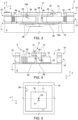
Figure 2 is a top-plan view of a microelectromechanical device in accordance with an embodiment of the present invention, integrated in the wafer ofFigure 1 ; -
Figure 3 is a cross-section of the microelectromechanical device ofFigure 2 , taken along line III-III ofFigure 2 ; -
Figure 4 is a cross-section of the microelectromechanical device ofFigure 2 , taken along line IV-IV ofFigure 2 ; -
Figure 5 shows an enlarged detail of the microelectromechanical device ofFigure 2 ; -
Figure 6 is a simplified block diagram of the test equipment ofFigure 1 ; -
Figure 7 is a simplified block diagram of the microelectromechanical device ofFigure 2 in use configuration; -
Figure 8 is a top-plan view of a microelectromechanical device in accordance with a different embodiment of the present invention; -
Figure 9 is a cross-section of the microelectromechanical device ofFigure 8 , taken along line IX-IX ofFigure 8 ; -
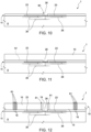
Figures 10-15 are cross-sections of the wafer incorporating the microelectromechanical device ofFigure 2 in successive processing steps of a method in accordance with an embodiment of the present invention. -
Figure 1 shows a top-plan view of asemiconductor wafer 1 and a plurality ofmicroelectromechanical devices 2 in accordance with an embodiment of the invention integrated in thesemiconductor wafer 1. In the case described and illustrated herein, themicroelectromechanical devices 2 are two detection-axis gyroscopes, as explained in detail hereinbelow. However, this should not be understood in a limiting sense. The integrated microelectromechanical devices may include gyroscopes of any type (uniaxial, biaxial, triaxial), as well as other inertial sensors (accelerometers, inclinometers) and, in general, microelectromechanical devices having a microstructure with movable parts. - In the example of
Figure 1 , eachmicroelectromechanical device 2 present in thewafer 1 comprises amicrostructure 3 andrespective pads 5, connected to themicrostructure 3. Atest machine 7, for example for EWS (Electrical Wafer Sorting) tests at the wafer level, is connected to thepads 5 to perform tests, at the wafer level, on the functionality of themicroelectromechanical devices 2, in particular of the spurious vibration modes of themicrostructures 3, as described in detail hereinbelow. -
Figures 2-4 show in greater detail a portion of thewafer 1 where one of themicroelectromechanical devices 2 is integrated. As may be seen fromFigures 2-4 , thewafer 1 comprises asubstrate 8 of semiconductor material, for example monocrystalline silicon, a firststructural layer 10, joined to thesubstrate 8 by afirst dielectric layer 11, and a secondstructural layer 12, joined to the firststructural layer 10 by asecond dielectric layer 13. The firststructural layer 10 and the secondstructural layer 12 may be semiconductor material layers grown by epitaxy (monocrystalline or polycrystalline epitaxial layers). Themicrostructure 3 is obtained from the firststructural layer 10 and from the secondstructural layer 12 by separating, by anisotropic etchings, respective portions of the firststructural layer 10 and of the secondstructural layer 12 from the rest of the firststructural layer 10 and of the secondstructural layer 12. - The
microstructure 3 comprises amovable mass 15, obtained from the firststructural layer 10, and atest structure 17, obtained essentially from the firststructural layer 10 and from the secondstructural layer 12 and provided with ananchor 18 for the mechanical and electrical connection to thesubstrate 8. - The first
structural layer 10 and the secondstructural layer 12 delimit acavity 19 wherein themovable mass 15 and thetest structure 17 are accommodated. In particular, the firststructural layer 10 forms a support frame for themovable mass 15. The secondstructural layer 12 in one embodiment supports thepads 5. Thefirst dielectric layer 11 and thesecond dielectric layer 13 are not present inside thecavity 19. - The
movable mass 15 is constrained to the firststructural layer 10 byelastic connection elements 16. In practice, thesubstrate 8, the firststructural layer 10, thefirst dielectric layer 11, the secondstructural layer 12 and thesecond dielectric layer 13 form a support body for the movable mass. In the embodiment described herein, theelastic connection elements 16 are configured to allow themovable mass 15 to oscillate in thecavity 19 with three translational degrees of freedom, parallel and perpendicular to asurface 8a of thesubstrate 8. Themovable mass 15 is also provided withdrive actuators 20, configured to oscillate the samemovable mass 15 along a drive X-axis parallel to thesurface 8a of thesubstrate 8. Themovable mass 15 further comprises one or more movableyaw detection electrodes 21, facing corresponding fixedyaw detection electrodes 22, rigidly connected to thesubstrate 8. The movableyaw detection electrodes 21 and the fixedyaw detection electrodes 22 define capacitors having flat faces parallel to the X axis, with variable capacitance as a function of displacements of themovable mass 15 along an Y axis parallel to thesurface 8a of thesubstrate 8 and perpendicular to the X axis. In the case of themicroelectromechanical device 2, themovable mass 15 translates, along the Y axis, in response to yaw movements, i.e. rotations around an axis perpendicular to thesurface 8a of thesubstrate 8. One of the sides of themovable mass 15, facing a respective fixedyaw detection electrode 22, may act as a movableyaw detection electrode 21. - Fixed pitch/
roll detection electrodes 23 are located on thesubstrate 8 and face themovable mass 15, which acts as a movable pitch/roll detection electrode. Themovable mass 15 and the fixed pitch/roll detection electrodes 23 define capacitors with variable capacitance as a function of displacements of themovable mass 15 along a Z axis perpendicular to the X axis and to the Y axis. In the case of themicroelectromechanical device 2, themovable mass 15 translates, along the Z axis, in response to pitch and/or roll movements, i.e. rotations around an axis parallel to thesurface 8a of thesubstrate 8. - The
movable mass 15, with all the movable detection electrodes, and all the fixed detection electrodes are connected torespective pads 5 of themicroelectromechanical device 1 throughconnection lines 26 formed on thesubstrate 8 and/or embedded therein. - The
test structure 17 comprises a semiconductor material body which forms theanchor 18, atest plate 25 and a group of fixedtest electrodes 27 and is fixed to thesubstrate 8. Thetest structure 17 is distinct from thedrive actuators 20 and from the fixeddetection electrodes - The
anchor 18, obtained essentially from the firststructural layer 10, includes a pillar fixed to abias pad 28 placed on thesubstrate 8 and is electrically (galvanically) isolated both from thesame substrate 8 and from themovable mass 15. Thebias pad 28 is connected to one of thepads 5 of themicroelectromechanical device 1 through one of the connection lines 26. In this manner, during the test step theanchor 18 and the entire test structure may be biased independently of themovable mass 15. - Furthermore, the
anchor 18 extends in the direction of the Z axis through anopening 30 in themovable mass 15. Theanchor 18 and theopening 30 have respective sides facing each other. In rest conditions, i.e. in the absence of forcing and external stresses, theanchor 18 is off-center with respect to theopening 30 in themovable mass 15. In one embodiment, in particular, a center C1 of theanchor 18 is offset with respect to a center C2 of theopening 30 in the direction of the Y axis, so that theanchor 18 is closer to one of the sides of themovable mass 15 delimiting theopening 30 in the direction of the Y axis than to the opposite side. The different distance causes a different capacitive coupling. Consequently, when a voltage is applied between themovable mass 15 and theanchor 18 of thetest structure 17, the electrostatic forces acting on themovable mass 15 are not balanced and themovable mass 15 moves along the Y axis. Theanchor 18 in practice defines a test actuator configured to apply test forces FY to themovable mass 15 in the direction of the Y axis. In the embodiment ofFigures 2-4 , themovable mass 15 is instead centered with respect to theopening 30 in the direction of the X axis. The forces in the direction of the X axis are therefore balanced and the capacitive coupling between themovable mass 15 and theanchor 18 does not affect the motion of the samemovable mass 15. - The
test plate 25 is obtained from the secondstructural layer 12, as are the fixedtest electrodes 27, and is connected to thesubstrate 8 through theanchor 18. Themovable mass 15 is arranged between thesubstrate 8 and thetest plate 25 of thetest structure 17. Therefore, themovable mass 15 has afirst side 15a facing thesubstrate 8 and asecond side 15b facing thetest plate 25. - The
movable mass 15 and thetest plate 25 face each other and are capacitively coupled. Therefore, a voltage applied between themovable mass 15 and thetest plate 25 of thetest structure 17 causes electrostatic forces which move themovable mass 15 in the direction of the Z axis. Thetest plate 25 thus defines a test actuator configured to apply test forces FZ to themovable mass 15 in the direction of the Z axis. - The fixed
test electrodes 27 are defined by respective flat semiconductor plates which extend from one side of thetest plate 25 parallel to an XZ plane defined by the X axis and the Z axis. The fixedtest electrodes 27 are capacitively coupled tomovable test electrodes 31 formed on one face of themovable mass 15 adjacent to thetest plate 25. More precisely, themovable test electrodes 31 are defined by respective flat semiconductor plates parallel to the XZ plane, obtained from the secondstructural layer 12, and are arranged in interdigitated configuration with respect to the fixedtest electrodes 27. A voltage applied between the fixedtest electrodes 27 of thetest structure 17 and themovable test electrodes 31 of themovable mass 15 causes electrostatic forces which move themovable mass 15 in the direction of the X axis. The fixedtest electrodes 27 thus define a test actuator configured to apply test forces FX to themovable mass 15 in the direction of the X axis. - With reference to
Figure 6 , during an EWS test step, thetest machine 7 is connected to thepads 5 of themicroelectromechanical devices 2, or at least selectively to groups thereof, integrated in the wafer 1 (for simplicityFigure 7 illustrates only onemicroelectromechanical device 1 connected to thetest machine 7;Figure 1 shows a greater number thereof). Thetest machine 7 comprises acontrol unit 35 and one or moretest signal generators 37, controlled by thecontrol unit 35. - The
test signal generator 37 is coupled torespective pads 5 so as to apply a test voltage VT between themovable mass 15 and thetest structure 17 under the control of thecontrol unit 35. The test voltage VT may be for example a sinusoidal voltage with frequency and amplitude controlled by thecontrol unit 35. For example, the frequency of the test voltage VT may vary over time so as to stress different spurious vibration modes of themicrostructure 3 of themicroelectromechanical devices 2. - The
control unit 35 also has inputs coupled topads 5 connected to the (fixed)detection electrodes movable mass 15. - In use, on the other hand, each
microelectromechanical device 2 obtained by dicing thewafer 1 is coupled to a respective control integrated circuit or ASIC (Application Specific Integrated Circuit) 50 which maintains themicrostructure 15 and thetest structure 17 at the same voltage, as shown inFigure 7 . The connection between themicrostructure 15 and thetest structure 17 may be obtained for example through aswitch 51 controlled by acontrol unit 52 of theASIC 50 or by a permanent direct connection. In this manner, during normal operation of themicroelectromechanical device 1, thetest structure 17 has no impact on the response of themovable mass 15 because the voltage between themovable mass 15 and thetest structure 17 is zero. - Owing to the capacitive coupling between the fixed
test electrodes 27 and themovable test electrodes 31, between theanchor 18 and themovable mass 15 in theopening 30 and between thetest plate 25 and themovable mass 15, the test voltage VT causes test forces FX, FY, FZ between themovable mass 15 and thetest structure 17 respectively along the X axis, along the Y axis and along the Z axis, as illustrated inFigures 3 and 4 . In turn, the test forces FX, FY, FZ excite the spurious vibration modes of themicrostructure 3 and the response is read through the sense signals SSENSE, which contain spurious contributions superimposed on the signals induced by the test voltage VT. Themicroelectromechanical devices 2 which have responses to the test voltage VT above programmed thresholds are marked as defective. - In practice, therefore, the
test structure 17 allows the effect of the spurious vibration modes of themicrostructures 3 at the wafer level to be examined. The defectivemicroelectromechanical devices 2 may be identified in a systematic manner and, once thewafer 1 has been diced, eliminated before the assembly operations. The test at the wafer level thus allows a considerable saving of method steps and materials used. - In terms of occupied area and sensitivity of the microelectromechanical devices, the
test structure 17 has an almost negligible impact, limited to the dimensions of theopening 30 in the XY plane. In other words, with the same rail area, the reduction of sensitivity due to that theopening 30 reduces the inertia of themovable mass 5 is not significant; in a dual manner, any increase in the dimensions of themovable mass 15 to compensate for theopening 30 would be extremely small. Thetest structure 17 is in fact mostly superimposed on themovable mass 15 and increases the overall dimensions of themicroelectromechanical device 1 mainly in the direction perpendicular to thesurface 8a of the substrate 8 (along the Z axis). However, the increase in dimensions in this direction is usually not critical. - The invention may advantageously be exploited in microelectromechanical devices, in particular gyroscopes, with any configuration of movable masses.
- For example, according to the embodiment illustrated in
Figures 8 and 9 , asemiconductor wafer 101 comprises a plurality ofmicroelectromechanical devices 102, in particular triaxial microelectromechanical gyroscopes, only one of which is shown for convenience. - Each
microelectromechanical device 102 has amicrostructure 103 which comprises a support body, fourmovable masses 115, arranged in specularly symmetrical pairs around a center C, and fourtest structures 117, each associated with a respectivemovable mass 115. The support body includes asubstrate 108 of thewafer 101, a firststructural layer 110, a firstdielectric layer 111, a secondstructural layer 112 and asecond dielectric layer 113. The firststructural layer 110 and the secondstructural layer 112 are of semiconductor material, for example grown by epitaxy. - The
movable masses 115 are constrained to the support body so as to oscillate in phase opposition in pairs, in a manner known per se. In particular, twomovable masses 115 oscillate in phase opposition along an X axis parallel to thesurface 108a of thesubstrate 108 and twomovable masses 115 oscillate in phase opposition along an Y axis parallel to thesurface 108a and perpendicular to the X axis. Furthermore, all themovable masses 115 oscillate in phase opposition in pairs around respective rotation axes Ra-Rd parallel to thesurface 108a of thesubstrate 108. - The
movable masses 115 are provided with respective systems ofmovable detection electrodes 121, capacitively coupled to respective fixeddetection electrodes 122 anchored to thesubstrate 108. Further fixeddetection electrodes 123 arranged on thesubstrate 108 are capacitively coupled to a face of a respectivemovable mass 115. Themovable masses 115, with all themovable detection electrodes 121, and all the fixeddetection electrodes respective pads 105 of themicroelectromechanical device 101 throughconnection lines 126 formed on thesubstrate 108 and/or embedded therein. -
Figure 9 shows two of themovable masses 115 and therelative test structures 117. It is understood that the other twomovable masses 115 andtest structures 117 are substantially identical to those shown inFigure 9 . - Like the
movable masses 115, thetest structures 117 are also arranged in specularly symmetrical pairs with respect to the center C of themicroelectromechanical device 101. Eachtest structure 117 comprises a semiconductor material body which forms ananchor 118, atest plate 125 and a group of fixedtest electrodes 127 and is fixed to thesubstrate 108, substantially as already described. More precisely, eachanchor 118 is fixed to arespective bias pad 128 placed on thesubstrate 108 and is electrically isolated both from thesame substrate 108 and from themovable mass 115. Thebias pads 128 are connected torespective pads 105 through the connection lines 126. - Each
anchor 118 extends in the direction of the Z axis through anopening 130 in the respectivemovable mass 115. As already described, theanchors 18 are off-center with respect to therespective openings 130. For example, theanchors 118 of thetest structures 117 associated with themovable masses 115 oscillating along the X axis are off-center in the direction of the Y axis, so as to define actuators which apply test forces FY1 according to the Y axis. Theanchors 118 of thetest structures 117 associated with themovable masses 115 oscillating along the Y axis are off-center in the direction of the X axis, so as to define actuators which apply test forces FX1 according to the X axis. - The
test plates 125 are connected to thesubstrate 108 through the respective anchors 118. Themovable masses 115 are arranged between thesubstrate 108 on one side and thetest plates 125 of therespective test structures 117 on the other side. Therefore, eachmovable mass 115 has afirst side 115a facing thesubstrate 108 and asecond side 115b facing thetest plate 125. - The
movable masses 115 and therespective test plates 125 face each other and are capacitively coupled. Thetest plates 125 thus define test actuators configured to apply electrostatic test forces FZ to the respectivemovable masses 115 in the direction of the Z axis. - The fixed
test electrodes 127 associated with themovable masses 115 oscillating along the X axis comprise respective flat semiconductor plates which extend on one side of therespective test plate 125 parallel to an XZ plane defined by the X axis and the Z axis. The fixedtest electrodes 127 are capacitively coupled arranged in interdigitated configuration tomovable test electrodes 131 formed on the respectivemovable masses 115. The fixedtest electrodes 127 associated with themovable masses 115 oscillating along the X axis thus define test actuators configured to apply test forces FX2 to the respectivemovable masses 15 in the direction of the X axis. - The fixed
test electrodes 127 associated with themovable masses 115 oscillating along the Y axis comprise respective flat semiconductor plates which extend on one side of therespective test plate 125 parallel to a YZ plane defined by the Y axis and the Z axis. The fixedtest electrodes 127 are capacitively coupled arranged in interdigitated configuration tomovable test electrodes 131 formed on the respectivemovable masses 115. The fixedtest electrodes 127 associated with themovable masses 115 oscillating along the Y axis thus define test actuators configured to apply test forces FY2 to the respectivemovable masses 115 in the direction of the Y axis. - During the test step, electrostatic forces directed according to the three axes X, Y, Z may be applied to the
movable masses 115 through therespective test structures 117 substantially as already described, so as to excite the possible spurious vibration modes of themicrostructure 103. Furthermore, themovable masses 115 may be forced into motion individually or simultaneously in various combinations (e.g., in opposite pairs or adjacent pairs) to have a wider range of stresses which may trigger spurious vibration modes. - The microelectromechanical device according to the invention may be obtained substantially using the method described in the European
patent application EP 3 912 953 A1 published on 11/24/2021 Figures 1-5 . However, it is understood that the same method may be applied for the embodiment ofFigures 8, 9 and, more generally, for any embodiment of the invention. In practice, themovable mass 15, thetest structure 17 and the fixed and movable detection electrodes are obtained from two structural layers grown epitaxially one on the other, as described in detail hereinbelow. - Initially (
Figure 10 ), the connection lines 26 and, on thesubstrate 8, the fixed pitch/roll detection electrodes 23 and thebias pad 28 are formed. Thefirst dielectric layer 11 is formed on thesubstrate 8 and is etched to form awindow 60 on thebias pad 28, in a position corresponding to theanchor 18. - The first
structural layer 10 is grown by epitaxy from a seed layer 10' deposited on the first dielectric layer 11 (Figure 11 ). The firststructural layer 10 then extends over thefirst dielectric layer 11 and contacts thebias pad 28 through thewindow 60. - The first
structural layer 10,Figure 12 , is then etched to define themovable mass 15, theelastic connection elements 16, theanchor 18, the fixed yaw detection electrodes 22 (not visible inFigure 12 ) and possibly other regions provided based on design preferences. For this purpose, thewafer 1 is covered by a resist mask not shown (first trench mask) and subject to a dry etching, formingtrenches 61, which completely traverse the firststructural layer 10. In this step, trenches (not shown) are also formed through the portion of the firststructural layer 10 intended to form themovable mass 15, which will have a lattice structure. The trenches will also serve in the subsequent steps for the removal of portions of thedielectric layer 11, to release themovable mass 15. The etching automatically stops on the firstelectric layer 11. - Subsequently,
Figure 13 , thesecond dielectric 13 is deposited, for a thickness T equal to a desired width of a gap between themovable mass 15 and thetest plate 25 which will be formed subsequently. Thesecond dielectric layer 13 partially fills thetrenches 61, for example for one third of their depth although this filling, as well as the filling extent and depth are not important. Thesecond dielectric layer 13 is then selectively etched and removed throughout its entire thickness, using a masking layer not shown, formingwindows 62 in positions corresponding to theanchor 18 and to regions of themovable mass 15 where themovable test electrodes 31 will have to be formed subsequently. - As shown in
Figure 14 , the secondstructural layer 12 is then grown, also in this case by epitaxy, starting from a second deposited seed layer 12' . The thickness of the secondstructural layer 12 is linked to the desired microelectro-mechanical structures. In general, the secondstructural layer 12 may be thinner than the firststructural layer 10, although the reverse may occur and the invention is not limited to any particular ratio between the thicknesses of thestructural layers - Then,
Figure 15 , the secondstructural layer 12 is etched. For this purpose, thewafer 1 is covered by a resist mask not shown (second trench mask) and subject to a dry etching. In this step, the portions of the secondstructural layer 12 not covered by the resist mask are removed throughout the entire thickness and the etching stops on the remaining portions of thesecond dielectric 13. In particular, in thisstep trenches 65 are opened which completely traverse the secondstructural layer 12 and thetest plate 25, the fixedtest electrodes 27 and themovable test electrodes 31 are defined. - Through the
trenches movable mass 15, thesecond dielectric layer 13 and thefirst dielectric layer 11 are in succession partially removed over and under themovable mass 15, between themovable mass 15 and thetest plate 25 and around theanchor 18. Themovable mass 15 is thus released and the structure ofFigures 2-4 is obtained. - Finally, it is clear that modifications and variations may be made to the microelectromechanical device, equipment and method described, without departing from the scope of the present invention, as defined in the attached claims.
- For example, the fixed and movable test electrodes may form a parallel-plate rather than an interdigitated-plate type actuator. In this case, the fixed and movable electrodes extend in a direction perpendicular (rather than parallel) to the electrostatic force applied to the movable mass.
- The anchor may be off-center with respect to the opening in the movable mass both with respect to the X axis and with respect to the Y axis and not only with respect to one of the two.
- In some embodiments, the test structure might be limited to the off-center pillar extending through the opening into the movable mass and possibly comprises further fixed and movable test electrodes obtained from the first structural layer.
Claims (17)
- A microelectromechanical device comprising:a support body (8, 10-13; 108, 110-113);at least one movable mass (15; 115) of semiconductor material, elastically constrained to the support body (8, 10-13; 108, 110-113) so as to be able to oscillate along one or more axes (X, Y, Z, Ra-Rd);fixed detection electrodes (22, 23; 122, 123) rigidly connected to the support body (8, 10-13; 108, 110-113) and capacitively coupled to the at least one movable mass (15; 115); andat least one test structure (17; 117) of semiconductor material, rigidly connected to the support body (8, 10-13; 108, 110-113) and distinct from the fixed detection electrodes (22, 23; 122, 123);wherein the at least one test structure (17; 117) is capacitively coupled to the at least one movable mass (15; 115) and is configured to apply electrostatic forces (FX, FY, FZ) to the at least one movable mass (15; 115) in response to a voltage between the at least one test structure (17; 117) and the at least one movable mass (15; 115).
- The device according to claim 1, wherein the at least one test structure (17; 117) is electrically isolated from the movable mass (15; 115) and from the substrate (8; 108).
- The device according to claim 1 or 2, wherein the support body (8, 10-13; 108, 110-113) includes a substrate (8; 108) of semiconductor material;wherein the at least one test structure (17; 117) comprises a first portion (25, 27; 125, 127) and a second portion (18, 28; 118, 128);wherein the at least one movable mass (15; 115) is arranged between the substrate (8; 108) and the first portion (25, 27; 125, 127) of the at least one test structure (17; 117) ;and wherein the second portion (18, 28; 118, 128) of the at least one test structure (17; 117) is anchored to the substrate (8; 108) and extends through the at least one movable mass (15; 115).
- The device according to claim 3, wherein the first portion (25, 27; 125, 127) of the at least one test structure (17; 117) comprises a test plate (25; 125) of semiconductor material and wherein the at least one movable mass (15; 115) has a first side (17a; 115a) facing the substrate (8; 108) and a second side (15b; 115b) facing the test plate (25; 125) .
- The device according to claim 3 or 4, wherein the first portion (25, 27; 125, 127) of the at least one test structure (17; 117) comprises fixed test electrodes (27; 127) and wherein the at least one movable mass (15; 115) comprises movable test electrodes (31; 131) capacitively coupled to the fixed test electrodes (27; 127).
- The device according to claim 5 dependent on claim 4, wherein the fixed test electrodes (27; 127) extend from the test plate (25; 125) and the movable test electrodes (31; 131) are arranged on the second side (15b; 115b) of the at least one movable mass (15; 115) facing the test plate (25; 125).
- The device according to claim 6, wherein the fixed test electrodes (27; 127) are defined by respective flat semiconductor plates extending from the test plate (25; 125) and the movable test electrodes (31; 131) are defined by respective flat semiconductor plates formed on a face of the movable mass (15; 115) adjacent to the test plate (25; 125) and wherein the fixed test electrodes (27; 127) and the movable test electrodes (31; 131) are interdigitated.
- The device according to any of claims 3 to 7, wherein the at least one movable mass (15; 115) has an opening (30; 130) and wherein the second portion (18, 28; 118, 128) of the at least one test structure (17; 117) comprises an anchor (18, 28; 118, 128) connecting the first portion (25, 27; 125, 127) of the at least one test structure (17; 117) to the substrate (8; 108) and extending through the opening (30; 130) in the at least one movable mass (15; 115).
- The device according to claim 8, wherein the anchor (18, 28; 118, 128) is off-center with respect to the opening (30; 130) .
- The device according to claim 9 dependent on claim 5, wherein the fixed test electrodes (27; 127) are configured to apply a first electrostatic test force (FX) in a first direction (X) parallel to a surface (8a; 108a) of the substrate (8; 108) and wherein the anchor (18, 28; 118, 128) is off-center with respect to the opening (30; 130) in a second direction (Y) parallel to the surface (8a; 108a) of the substrate (8; 108) and perpendicular to the first direction (X).
- The device according to any of the preceding claims, comprising a plurality of movable masses (115) of semiconductor material, elastically constrained to the support body (108, 110-113) so as to be able to oscillate with respective relative degrees of freedom; anda plurality of test structures (117) of semiconductor material, rigidly connected to the support body (108, 110-113), distinct from the fixed detection electrodes (122, 123) and each capacitively coupled to a respective of the movable masses (115);wherein the movable masses (115) and the respective test structures (117) are arranged in symmetrical pairs with respect to a center (C).
- The device according to any of the preceding claims, wherein in response to variations over time of the voltage between the at least one test structure (17; 117) and the at least one movable mass (15; 115), the test forces (FX, FY, FZ) between the movable mass (15) and the test structure (17) are configured to excite spurious vibration modes of a microstructure (3) comprising the movable mass (15) and the test structure (17).
- The device according to any of the preceding claims, comprising pads (5; 105) accessible from the outside, wherein the at least one movable mass (15; 115) and the at least one test structure (17; 117) are electrically coupled to respective pads (5; 105).
- The device according to any of the preceding claims, comprising a control integrated circuit (50) connected to the pads (5) and configured to set the voltage between the at least one movable mass (15) and the at least one test structure (17) to zero in use.
- A test equipment for testing microelectromechanical devices comprising a semiconductor wafer (1) integrating a plurality of microelectromechanical devices (2) according to claim 13 and a test machine (7) connected to the pads (5) of the microelectromechanical devices and comprising at least one test signal generator (37), configured to apply a test voltage (VT) between the pads (5; 105) respectively coupled to the at least one movable mass (15) and to the at least one test structure (17).
- A method for manufacturing a microelectromechanical device, comprising:forming a support body (8, 10-13; 108, 110-113);forming at least one movable mass (15; 115) of semiconductor material, elastically constrained to the support body (8, 10-13; 108, 110-113) so as to be able to oscillate along one or more axes (X, Y, Z, Ra-Rd) along one or more axes (X, Y, Z, Ra-Rd);forming fixed detection electrodes (22, 23; 122, 123) rigidly connected to the support body (8, 10-13; 108, 110-113) and capacitively coupled to the at least one movable mass (15; 115); andforming at least one test structure (17; 117) of semiconductor material, rigidly connected to the support body (8, 10-13; 108, 110-113) and distinct from the fixed detection electrodes (22, 23; 122, 123);wherein the at least one test structure (17; 117) is capacitively coupled to the at least one movable mass (15; 115) and is configured to apply electrostatic forces (FX, FY, FZ) to the at least one movable mass (15; 115) in response to a voltage between the at least one test structure (17; 117) and the at least one movable mass (15; 115).
- The method according to claim 16, wherein:forming the support body (8, 10-13; 108, 110-113) comprises forming a first dielectric layer (11; 111), growing a first structural layer (10; 110) on the first dielectric layer (11; 111) by epitaxy from a first deposited seed layer (10'), forming a second dielectric layer (13; 113) on the first structural layer (10; 110) and growing a second structural layer (12; 112) on the second dielectric layer (13; 113) by epitaxy from a second deposited seed layer (12');forming the at least one movable mass (15; 115) comprises forming a first window (60) in the first dielectric layer (11; 111) before growing the first structural layer (10; 110) and selectively etching the first structural layer (10; 110) up to the first dielectric layer (11; 111); andforming the at least one test structure (17; 117) comprises forming second windows (62) in the second dielectric layer (13; 113) before growing the second structural layer (12; 112) and selectively etching the second structural layer (12; 112) up to the second dielectric layer (13; 113).
Applications Claiming Priority (1)
| Application Number | Priority Date | Filing Date | Title |
|---|---|---|---|
| IT102022000024732A IT202200024732A1 (en) | 2022-11-30 | 2022-11-30 | MICROELECTROMECHANICAL DEVICE WITH TEST STRUCTURE, TEST EQUIPMENT FOR TESTING MICROELECTROMECHANICAL DEVICES AND METHOD FOR MANUFACTURING A MICROELECTROMECHANICAL DEVICE |
Publications (2)
| Publication Number | Publication Date |
|---|---|
| EP4379320A1 true EP4379320A1 (en) | 2024-06-05 |
| EP4379320B1 EP4379320B1 (en) | 2025-12-31 |
Family
ID=85225086
Family Applications (1)
| Application Number | Title | Priority Date | Filing Date |
|---|---|---|---|
| EP23211935.4A Active EP4379320B1 (en) | 2022-11-30 | 2023-11-24 | Microelectromechanical device with test structure, test equipment for testing microelectromechanical devices and method for manufacturing a microelectromechanical device |
Country Status (4)
| Country | Link |
|---|---|
| US (1) | US20240175682A1 (en) |
| EP (1) | EP4379320B1 (en) |
| CN (1) | CN118108173A (en) |
| IT (1) | IT202200024732A1 (en) |
Citations (2)
| Publication number | Priority date | Publication date | Assignee | Title |
|---|---|---|---|---|
| US20160169933A1 (en) * | 2014-12-15 | 2016-06-16 | Robert Bosch Gmbh | Method for testing the functionality of a rotation rate sensor |
| EP3912953A1 (en) | 2020-05-20 | 2021-11-24 | STMicroelectronics S.r.l. | Process for manufacturing a micro-electro-mechanical device, in particular a movement sensor with capacitive control/detection, and mems device |
Family Cites Families (19)
| Publication number | Priority date | Publication date | Assignee | Title |
|---|---|---|---|---|
| US6257059B1 (en) * | 1999-09-24 | 2001-07-10 | The Charles Stark Draper Laboratory, Inc. | Microfabricated tuning fork gyroscope and associated three-axis inertial measurement system to sense out-of-plane rotation |
| US6750152B1 (en) * | 1999-10-01 | 2004-06-15 | Delphi Technologies, Inc. | Method and apparatus for electrically testing and characterizing formation of microelectric features |
| US6619123B2 (en) * | 2001-06-04 | 2003-09-16 | Wisconsin Alumni Research Foundation | Micromachined shock sensor |
| DE102004058183A1 (en) * | 2004-12-02 | 2006-06-08 | Robert Bosch Gmbh | Sensor with self-test |
| TWI317812B (en) * | 2006-12-22 | 2009-12-01 | Delta Electronics Inc | Capacitance acceleration sensing structure |
| US7677099B2 (en) * | 2007-11-05 | 2010-03-16 | Invensense Inc. | Integrated microelectromechanical systems (MEMS) vibrating mass Z-axis rate sensor |
| KR20100080555A (en) * | 2007-11-08 | 2010-07-08 | 로베르트 보쉬 게엠베하 | Yaw rate sensor having two sensitive axes |
| US8783103B2 (en) * | 2009-08-21 | 2014-07-22 | Analog Devices, Inc. | Offset detection and compensation for micromachined inertial sensors |
| US20130001550A1 (en) * | 2011-06-29 | 2013-01-03 | Invensense, Inc. | Hermetically sealed mems device with a portion exposed to the environment with vertically integrated electronics |
| US9714842B2 (en) * | 2011-09-16 | 2017-07-25 | Invensense, Inc. | Gyroscope self test by applying rotation on coriolis sense mass |
| US9069006B2 (en) * | 2012-04-05 | 2015-06-30 | Fairchild Semiconductor Corporation | Self test of MEMS gyroscope with ASICs integrated capacitors |
| US9752944B2 (en) * | 2014-03-12 | 2017-09-05 | Stmicroelectronics S.R.L. | Microelectromechanical sensing structure for a pressure sensor including a deformable test structure |
| ITUA20162160A1 (en) * | 2016-03-31 | 2017-10-01 | St Microelectronics Srl | MICROMECHANICAL STRUCTURE FOR DETECTION OF A MEMS MULTI-FACTORY GYROSCOPE, HAVING REDUCED DERIVED FROM RELATED ELECTRICAL CHARACTERISTICS |
| IT201600081227A1 (en) * | 2016-08-02 | 2018-02-02 | St Microelectronics Srl | MEMS GYROSCOPE WITH FREQUENCY REGULATION AND ELECTROSTATIC CANCELLATION OF THE SQUARE ERROR |
| IT201700099412A1 (en) * | 2017-09-05 | 2019-03-05 | St Microelectronics Srl | MEMS GYROSCOPE WITH MISMATCH ADJUSTMENT BETWEEN PILOT FREQUENCY AND DETECTION FREQUENCY |
| IT201800001092A1 (en) * | 2018-01-16 | 2019-07-16 | St Microelectronics Srl | MICROELECTROMECHANICAL PIEZORESISTIVE PRESSURE SENSOR WITH SELF-DIAGNOSTIC CAPACITY AND RELATED MANUFACTURING PROCESS |
| IT201900010698A1 (en) * | 2019-07-02 | 2021-01-02 | St Microelectronics Srl | SYSTEM AND METHOD OF DIAGNOSIS OF THE WORKING STATE OF A MICROELECTROMECHANICAL SENSOR |
| US12017907B2 (en) * | 2021-01-27 | 2024-06-25 | Invensense, Inc. | Capacitance gap measurement |
| IT202200014548A1 (en) * | 2022-07-11 | 2024-01-11 | St Microelectronics Srl | SENSING STRUCTURE FOR A MEMS ACCELEROMETER WITH IMPROVED PERFORMANCE AND RELATED MANUFACTURING PROCEDURE |
-
2022
- 2022-11-30 IT IT102022000024732A patent/IT202200024732A1/en unknown
-
2023
- 2023-11-20 US US18/515,075 patent/US20240175682A1/en active Pending
- 2023-11-24 EP EP23211935.4A patent/EP4379320B1/en active Active
- 2023-11-28 CN CN202311603477.4A patent/CN118108173A/en active Pending
Patent Citations (2)
| Publication number | Priority date | Publication date | Assignee | Title |
|---|---|---|---|---|
| US20160169933A1 (en) * | 2014-12-15 | 2016-06-16 | Robert Bosch Gmbh | Method for testing the functionality of a rotation rate sensor |
| EP3912953A1 (en) | 2020-05-20 | 2021-11-24 | STMicroelectronics S.r.l. | Process for manufacturing a micro-electro-mechanical device, in particular a movement sensor with capacitive control/detection, and mems device |
Also Published As
| Publication number | Publication date |
|---|---|
| CN118108173A (en) | 2024-05-31 |
| IT202200024732A1 (en) | 2024-05-30 |
| US20240175682A1 (en) | 2024-05-30 |
| EP4379320B1 (en) | 2025-12-31 |
Similar Documents
| Publication | Publication Date | Title |
|---|---|---|
| US7892876B2 (en) | Three-axis accelerometers and fabrication methods | |
| EP1626283B1 (en) | Micro-electromechanical structure, in particular accelerometer, with improved insensitivity to thermomechanical stresses | |
| US5728936A (en) | Rotary speed sensor | |
| US5576250A (en) | Process for the production of accelerometers using silicon on insulator technology | |
| KR101105059B1 (en) | Method of making an x-y axis dual-mass tuning fork gyroscope with vertically integrated electronics and wafer-scale hermetic packaging | |
| US5889207A (en) | Micromechanical rate of rotation sensor having ring with drive element and detection element | |
| KR100492105B1 (en) | Vertical MEMS gyroscope by horizontal driving and it's fabrication method | |
| US9346670B2 (en) | MEMS device with differential vertical sense electrodes | |
| US9279822B2 (en) | Micromechanical structure and method for manufacturing a micromechanical structure | |
| CN101939653A (en) | Have the vertical integrated electron device and the X-Y axis dual-mass tuning fork gyroscope of wafer-level seal formula encapsulation | |
| US7505245B2 (en) | Semiconductor physical quantity sensor and method for manufacturing the same | |
| EP4024054B1 (en) | Mems vibrating beam accelerometer with built-in test actuators | |
| US20050140356A1 (en) | Multiaxial micromachined differential accelerometer | |
| EP4379320B1 (en) | Microelectromechanical device with test structure, test equipment for testing microelectromechanical devices and method for manufacturing a microelectromechanical device | |
| Kim et al. | An x-axis single-crystalline silicon microgyroscope fabricated by the extended SBM process | |
| Scheeper et al. | Development of a modal analysis accelerometer based on a tunneling displacement transducer | |
| US12540952B2 (en) | Microelectromechanical sensor device with active offset compensation | |
| EP2090866A1 (en) | Dynamic quantity sensor and method of manufacturing it | |
| EP4553449A1 (en) | Microelectromechanical device with movable mass and stopping structure having improved mechanical robustness | |
| US20250042718A1 (en) | Microelectromechanical device with recovery from stiction conditions | |
| JP5292825B2 (en) | Method for manufacturing mechanical quantity sensor | |
| JPH06160421A (en) | Oscillatory type acceleration sensor | |
| Garcia et al. | Double-Proof Mass SOI-Based Matryoshka-Like 3-Axis MEMS Accelerometer |
Legal Events
| Date | Code | Title | Description |
|---|---|---|---|
| PUAI | Public reference made under article 153(3) epc to a published international application that has entered the european phase |
Free format text: ORIGINAL CODE: 0009012 |
|
| STAA | Information on the status of an ep patent application or granted ep patent |
Free format text: STATUS: THE APPLICATION HAS BEEN PUBLISHED |
|
| AK | Designated contracting states |
Kind code of ref document: A1 Designated state(s): AL AT BE BG CH CY CZ DE DK EE ES FI FR GB GR HR HU IE IS IT LI LT LU LV MC ME MK MT NL NO PL PT RO RS SE SI SK SM TR |
|
| STAA | Information on the status of an ep patent application or granted ep patent |
Free format text: STATUS: REQUEST FOR EXAMINATION WAS MADE |
|
| 17P | Request for examination filed |
Effective date: 20241205 |
|
| GRAP | Despatch of communication of intention to grant a patent |
Free format text: ORIGINAL CODE: EPIDOSNIGR1 |
|
| STAA | Information on the status of an ep patent application or granted ep patent |
Free format text: STATUS: GRANT OF PATENT IS INTENDED |
|
| INTG | Intention to grant announced |
Effective date: 20250724 |
|
| GRAS | Grant fee paid |
Free format text: ORIGINAL CODE: EPIDOSNIGR3 |
|
| GRAA | (expected) grant |
Free format text: ORIGINAL CODE: 0009210 |
|
| STAA | Information on the status of an ep patent application or granted ep patent |
Free format text: STATUS: THE PATENT HAS BEEN GRANTED |
|
| AK | Designated contracting states |
Kind code of ref document: B1 Designated state(s): AL AT BE BG CH CY CZ DE DK EE ES FI FR GB GR HR HU IE IS IT LI LT LU LV MC ME MK MT NL NO PL PT RO RS SE SI SK SM TR |
|
| REG | Reference to a national code |
Ref country code: CH Ref legal event code: F10 Free format text: ST27 STATUS EVENT CODE: U-0-0-F10-F00 (AS PROVIDED BY THE NATIONAL OFFICE) Effective date: 20251231 Ref country code: GB Ref legal event code: FG4D |
|
| REG | Reference to a national code |
Ref country code: DE Ref legal event code: R096 Ref document number: 602023010423 Country of ref document: DE |
|
| REG | Reference to a national code |
Ref country code: IE Ref legal event code: FG4D |
|
| REG | Reference to a national code |
Ref country code: LT Ref legal event code: MG9D |
|
| PG25 | Lapsed in a contracting state [announced via postgrant information from national office to epo] |
Ref country code: NO Free format text: LAPSE BECAUSE OF FAILURE TO SUBMIT A TRANSLATION OF THE DESCRIPTION OR TO PAY THE FEE WITHIN THE PRESCRIBED TIME-LIMIT Effective date: 20260331 |
|
| PG25 | Lapsed in a contracting state [announced via postgrant information from national office to epo] |
Ref country code: FI Free format text: LAPSE BECAUSE OF FAILURE TO SUBMIT A TRANSLATION OF THE DESCRIPTION OR TO PAY THE FEE WITHIN THE PRESCRIBED TIME-LIMIT Effective date: 20251231 Ref country code: HR Free format text: LAPSE BECAUSE OF FAILURE TO SUBMIT A TRANSLATION OF THE DESCRIPTION OR TO PAY THE FEE WITHIN THE PRESCRIBED TIME-LIMIT Effective date: 20251231 |
|
| PG25 | Lapsed in a contracting state [announced via postgrant information from national office to epo] |
Ref country code: RS Free format text: LAPSE BECAUSE OF FAILURE TO SUBMIT A TRANSLATION OF THE DESCRIPTION OR TO PAY THE FEE WITHIN THE PRESCRIBED TIME-LIMIT Effective date: 20260331 |
|
| PG25 | Lapsed in a contracting state [announced via postgrant information from national office to epo] |
Ref country code: LV Free format text: LAPSE BECAUSE OF FAILURE TO SUBMIT A TRANSLATION OF THE DESCRIPTION OR TO PAY THE FEE WITHIN THE PRESCRIBED TIME-LIMIT Effective date: 20251231 |
|
| PG25 | Lapsed in a contracting state [announced via postgrant information from national office to epo] |
Ref country code: BG Free format text: LAPSE BECAUSE OF FAILURE TO SUBMIT A TRANSLATION OF THE DESCRIPTION OR TO PAY THE FEE WITHIN THE PRESCRIBED TIME-LIMIT Effective date: 20251231 |
|
| REG | Reference to a national code |
Ref country code: NL Ref legal event code: MP Effective date: 20251231 |