EP4378882A1 - Micromechanical environmental barrier chip and method for manufacturing same - Google Patents
Micromechanical environmental barrier chip and method for manufacturing same Download PDFInfo
- Publication number
- EP4378882A1 EP4378882A1 EP22210912.6A EP22210912A EP4378882A1 EP 4378882 A1 EP4378882 A1 EP 4378882A1 EP 22210912 A EP22210912 A EP 22210912A EP 4378882 A1 EP4378882 A1 EP 4378882A1
- Authority
- EP
- European Patent Office
- Prior art keywords
- environmental barrier
- micromechanical
- substrate
- barrier structure
- chip
- Prior art date
- Legal status (The legal status is an assumption and is not a legal conclusion. Google has not performed a legal analysis and makes no representation as to the accuracy of the status listed.)
- Granted
Links
Images











Classifications
-
- B—PERFORMING OPERATIONS; TRANSPORTING
- B81—MICROSTRUCTURAL TECHNOLOGY
- B81B—MICROSTRUCTURAL DEVICES OR SYSTEMS, e.g. MICROMECHANICAL DEVICES
- B81B7/00—Microstructural systems ; Auxiliary parts of microstructural devices or systems
- B81B7/0009—Structural features, others than packages, for protecting a device against environmental influences
- B81B7/0029—Protection against environmental influences not provided for in groups B81B7/0012 - B81B7/0025
-
- B—PERFORMING OPERATIONS; TRANSPORTING
- B81—MICROSTRUCTURAL TECHNOLOGY
- B81B—MICROSTRUCTURAL DEVICES OR SYSTEMS, e.g. MICROMECHANICAL DEVICES
- B81B7/00—Microstructural systems ; Auxiliary parts of microstructural devices or systems
- B81B7/0032—Packages or encapsulation
- B81B7/0045—Packages or encapsulation for reducing stress inside of the package structure
- B81B7/0048—Packages or encapsulation for reducing stress inside of the package structure between the MEMS die and the substrate
-
- B—PERFORMING OPERATIONS; TRANSPORTING
- B81—MICROSTRUCTURAL TECHNOLOGY
- B81B—MICROSTRUCTURAL DEVICES OR SYSTEMS, e.g. MICROMECHANICAL DEVICES
- B81B7/00—Microstructural systems ; Auxiliary parts of microstructural devices or systems
- B81B7/02—Microstructural systems ; Auxiliary parts of microstructural devices or systems containing distinct electrical or optical devices of particular relevance for their function, e.g. microelectro-mechanical systems [MEMS]
-
- B—PERFORMING OPERATIONS; TRANSPORTING
- B81—MICROSTRUCTURAL TECHNOLOGY
- B81C—PROCESSES OR APPARATUS SPECIALLY ADAPTED FOR THE MANUFACTURE OR TREATMENT OF MICROSTRUCTURAL DEVICES OR SYSTEMS
- B81C1/00—Manufacture or treatment of devices or systems in or on a substrate
- B81C1/00015—Manufacture or treatment of devices or systems in or on a substrate for manufacturing microsystems
- B81C1/00261—Processes for packaging MEMS devices
- B81C1/00277—Processes for packaging MEMS devices for maintaining a controlled atmosphere inside of the cavity containing the MEMS
- B81C1/00285—Processes for packaging MEMS devices for maintaining a controlled atmosphere inside of the cavity containing the MEMS using materials for controlling the level of pressure, contaminants or moisture inside of the package, e.g. getters
-
- B—PERFORMING OPERATIONS; TRANSPORTING
- B81—MICROSTRUCTURAL TECHNOLOGY
- B81B—MICROSTRUCTURAL DEVICES OR SYSTEMS, e.g. MICROMECHANICAL DEVICES
- B81B3/00—Devices comprising flexible or deformable elements, e.g. comprising elastic tongues or membranes
- B81B3/0064—Constitution or structural means for improving or controlling the physical properties of a device
- B81B3/0067—Mechanical properties
- B81B3/0072—For controlling internal stress or strain in moving or flexible elements, e.g. stress compensating layers
-
- B—PERFORMING OPERATIONS; TRANSPORTING
- B82—NANOTECHNOLOGY
- B82Y—SPECIFIC USES OR APPLICATIONS OF NANOSTRUCTURES; MEASUREMENT OR ANALYSIS OF NANOSTRUCTURES; MANUFACTURE OR TREATMENT OF NANOSTRUCTURES
- B82Y40/00—Manufacture or treatment of nanostructures
-
- H—ELECTRICITY
- H04—ELECTRIC COMMUNICATION TECHNIQUE
- H04R—LOUDSPEAKERS, MICROPHONES, GRAMOPHONE PICK-UPS OR LIKE ACOUSTIC ELECTROMECHANICAL TRANSDUCERS; ELECTRIC HEARING AIDS; PUBLIC ADDRESS SYSTEMS
- H04R31/00—Apparatus or processes specially adapted for the manufacture of transducers or diaphragms therefor
- H04R31/003—Apparatus or processes specially adapted for the manufacture of transducers or diaphragms therefor for diaphragms or their outer suspension
-
- B—PERFORMING OPERATIONS; TRANSPORTING
- B81—MICROSTRUCTURAL TECHNOLOGY
- B81B—MICROSTRUCTURAL DEVICES OR SYSTEMS, e.g. MICROMECHANICAL DEVICES
- B81B2201/00—Specific applications of microelectromechanical systems
- B81B2201/02—Sensors
- B81B2201/0257—Microphones or microspeakers
-
- B—PERFORMING OPERATIONS; TRANSPORTING
- B81—MICROSTRUCTURAL TECHNOLOGY
- B81B—MICROSTRUCTURAL DEVICES OR SYSTEMS, e.g. MICROMECHANICAL DEVICES
- B81B2201/00—Specific applications of microelectromechanical systems
- B81B2201/10—Microfilters, e.g. for gas or fluids
-
- B—PERFORMING OPERATIONS; TRANSPORTING
- B81—MICROSTRUCTURAL TECHNOLOGY
- B81B—MICROSTRUCTURAL DEVICES OR SYSTEMS, e.g. MICROMECHANICAL DEVICES
- B81B2203/00—Basic microelectromechanical structures
- B81B2203/03—Static structures
- B81B2203/0353—Holes
-
- B—PERFORMING OPERATIONS; TRANSPORTING
- B81—MICROSTRUCTURAL TECHNOLOGY
- B81B—MICROSTRUCTURAL DEVICES OR SYSTEMS, e.g. MICROMECHANICAL DEVICES
- B81B2207/00—Microstructural systems or auxiliary parts thereof
- B81B2207/11—Structural features, others than packages, for protecting a device against environmental influences
- B81B2207/115—Protective layers applied directly to the device before packaging
-
- B—PERFORMING OPERATIONS; TRANSPORTING
- B81—MICROSTRUCTURAL TECHNOLOGY
- B81C—PROCESSES OR APPARATUS SPECIALLY ADAPTED FOR THE MANUFACTURE OR TREATMENT OF MICROSTRUCTURAL DEVICES OR SYSTEMS
- B81C2201/00—Manufacture or treatment of microstructural devices or systems
- B81C2201/01—Manufacture or treatment of microstructural devices or systems in or on a substrate
- B81C2201/0101—Shaping material; Structuring the bulk substrate or layers on the substrate; Film patterning
- B81C2201/0128—Processes for removing material
- B81C2201/013—Etching
- B81C2201/0132—Dry etching, i.e. plasma etching, barrel etching, reactive ion etching [RIE], sputter etching or ion milling
-
- H—ELECTRICITY
- H04—ELECTRIC COMMUNICATION TECHNIQUE
- H04R—LOUDSPEAKERS, MICROPHONES, GRAMOPHONE PICK-UPS OR LIKE ACOUSTIC ELECTROMECHANICAL TRANSDUCERS; ELECTRIC HEARING AIDS; PUBLIC ADDRESS SYSTEMS
- H04R1/00—Details of transducers, loudspeakers or microphones
- H04R1/02—Casings; Cabinets ; Supports therefor; Mountings therein
- H04R1/023—Screens for loudspeakers
-
- H—ELECTRICITY
- H04—ELECTRIC COMMUNICATION TECHNIQUE
- H04R—LOUDSPEAKERS, MICROPHONES, GRAMOPHONE PICK-UPS OR LIKE ACOUSTIC ELECTROMECHANICAL TRANSDUCERS; ELECTRIC HEARING AIDS; PUBLIC ADDRESS SYSTEMS
- H04R2201/00—Details of transducers, loudspeakers or microphones covered by H04R1/00 but not provided for in any of its subgroups
- H04R2201/003—Mems transducers or their use
-
- H—ELECTRICITY
- H04—ELECTRIC COMMUNICATION TECHNIQUE
- H04R—LOUDSPEAKERS, MICROPHONES, GRAMOPHONE PICK-UPS OR LIKE ACOUSTIC ELECTROMECHANICAL TRANSDUCERS; ELECTRIC HEARING AIDS; PUBLIC ADDRESS SYSTEMS
- H04R2201/00—Details of transducers, loudspeakers or microphones covered by H04R1/00 but not provided for in any of its subgroups
- H04R2201/02—Details casings, cabinets or mounting therein for transducers covered by H04R1/02 but not provided for in any of its subgroups
- H04R2201/029—Manufacturing aspects of enclosures transducers
-
- H—ELECTRICITY
- H04—ELECTRIC COMMUNICATION TECHNIQUE
- H04R—LOUDSPEAKERS, MICROPHONES, GRAMOPHONE PICK-UPS OR LIKE ACOUSTIC ELECTROMECHANICAL TRANSDUCERS; ELECTRIC HEARING AIDS; PUBLIC ADDRESS SYSTEMS
- H04R2231/00—Details of apparatus or processes specially adapted for the manufacture of transducers or diaphragms therefor covered by H04R31/00, not provided for in its subgroups
- H04R2231/001—Moulding aspects of diaphragm or surround
Definitions
- Embodiments of the present disclosure relate to a micromechanical environmental barrier chip for providing a protection for MEMS microphones or MEMS speakers against ingress of environmental solid, gaseous and/or moist particles. Further embodiments relate to a manufacturing method thereof.
- MEMS microelectromechanical system
- EBs external and large environmental barriers
- a microstructured environmental barrier for MEMS-based acoustic elements comprising a small form factor while providing reliable and robust protection against ingress of environmental solid, gaseous and/or moist particles. It would further be desirable to provide a manufacturing method thereof that enables a reduction in production costs.
- Said method comprises a step of providing a substrate having a first surface and an opposite second surface, a step of depositing a material layer onto the first surface of the substrate, the material layer having a different etch rate than the substrate, and a step of creating a microstructured micromechanical environmental barrier structure on top of the material layer by applying a microstructuring process.
- the method further comprises a step of applying an anisotropic etching process comprising at least one etching step for anisotropically etching from the second surface towards the first surface of the substrate so as to create at least a first cavity underneath the micromechanical environmental barrier structure, the cavity extending between the second surface and the material layer.
- the method further comprises a step of removing the material layer residing inside the cavity in order to expose the environmental barrier structure.
- Method steps which are depicted by means of a block diagram and which are described with reference to said block diagram may also be executed in an order different from the depicted and/or described order. Furthermore, method steps concerning a particular feature of a device may be replaceable with said feature of said device, and the other way around.
- Figure 1 shows a schematic block diagram of the herein described innovative method according to an embodiment. The single method steps may be executed in a different order than depicted and described in the following.
- a substrate may be provided, said substrate having a first surface and an opposite second surface.
- a material layer may be deposited onto the first surface of the substrate, the material layer having a different etch characteristic than the substrate.
- An etch characteristic may include a certain selectivity.
- the selectivity describes an etch ratio between two different materials. For example, if the selectivity is 2:1, then a first material will be etched/removed two times faster than a second material, when applying the same etching process for the same time duration on both materials.
- a microstructured micromechanical environmental barrier structure may be provided on top of the material layer by applying a microstructuring process.
- an anisotropic etching process may be performed comprising at least one etching step for anisotropically etching through the substrate (e.g. from the second surface towards the first surface of the substrate) until reaching the material layer so as to create at least a first cavity opposite (e.g. underneath) the micromechanical environmental barrier structure, the cavity extending between the second surface and the material layer.
- any of the material layer that resides inside the cavity may be removed in order to expose the environmental barrier structure.
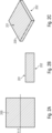
- Figures 2A to 5C show a structural description of the innovative method.
- Figures 2A , 3A , 4A and 5A show a top view onto the substrate 200 to be processed.
- Figures 2B , 3B , 4B and 5B show a cross-sectional view along the section line A-A.
- Figures 2C , 3C , 4C and 5C show a perspective view of the substrate 200.
- a substrate 200 is depicted, the substrate 200 having a first surface 201 and an opposite second surface 202.
- the substrate 200 may consist of, or comprise, a semiconductor material, such as silicon, for example.
- the substrate 200 may consist of, or comprise, glass, (poly-)imide, plastics or the like.
- the substrate 200 may be flexible or rigid.
- Figures 3A to 3C show a further method step.
- a material layer 210 may be deposited onto the first surface 201 of the substrate 200.
- the material layer 210 may be deposited completely over the entire first surface 201.
- the material layer 210 may comprise a different etch characteristic than the substrate 200.
- the material layer 210 and the substrate 200 may comprise a high selectivity for one and the same etchant.
- the selectivity describes the etch ratio between the material layer 210 and the substrate 200.
- the substrate 200 may be etched/removed significantly faster than the material layer 210.
- the substrate 210 may be completely removed while the material layer 210 is not noticeably etched/removed.
- the material layer 210 may serve the purpose of an etch stop layer.
- the material layer 210 may consist of or comprise tetraethyl orthosilicate, formally named tetraethoxysilane (TEOS), or other oxide (e.g., thermal silicon dioxides - SiO 2 -, atomic layer deposited oxide) and nitride (e.g., silicon nitride) materials. These materials have an insulating characteristic.
- TEOS tetraethyl orthosilicate
- silicon silicon
- FIGS 4A to 4C show a further method step.
- a microstructured micromechanical environmental barrier structure 220 may be created on top of the material layer 210.
- the micromechanical environmental barrier structure 220 may be formed by applying a microstructuring process, e.g., a surface MEMS micromachining process.
- the micromechanical environmental barrier structure 220 may be provided as an air permeable mesh, as depicted, or as a perforated air permeable membrane.
- the micromechanical environmental barrier structure 220 may comprise a circular or rectangular shape, while other geometrical shapes are possible.
- the micromechanical environmental barrier structure 220 may comprise vertically extending rib structures 221 that may extend through the material layer 210 and penetrate into the substrate 200, as shown in Figure 4B .
- the rib structures 210 may be arranged in a cross-wise manner thereby creating a mesh structure.
- the micromechanical environmental barrier structure 220 may be fabricated using wafer-level front-end processing.
- a main layer of the micromechanical environmental barrier structure 220 may comprise various materials used in front-end semiconductor processing, which include but are not limited to silicon, nitride, stacked silicon/nitride, and polymeric materials, e.g., polyimide, poly(methyl methacrylate) (PMMA), polydimethylsiloxane (PDMS), SU-8, and benzocyclobutene (BCB).
- the micromechanical environmental barrier structure 220 may be rigid and may provide sufficient large hole openings (e.g., 10 ⁇ m to 40 ⁇ m) to avoid high loss of signal-to-noise ratio (SNR) and sensitivity.
- SNR signal-to-noise ratio
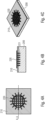
- Figures 5A to 5C show a further method step.
- An anisotropic etching process e.g. Reactive Ion Etching (RIE) using a Bosch etching process, may be applied comprising at least one etching step for anisotropically etching from the second surface 202 towards the first surface 201 of the substrate 200 so as to create at least a first cavity 230 underneath (i.e. opposite to) the micromechanical environmental barrier structure 220.
- the cavity 230 may extend completely through the substrate 200. Therefore, the cavity 230 may also be referred to as an opening or a through hole.
- the material layer 210 may serve as an etch stop layer. Accordingly, the substrate 200 may be etched until the etchant reaches the material layer 210. Even though not explicitly shown in Figures 5A to 5C , some of the material layer 210 may remain underneath the micromechanical environmental barrier structure 220, i.e. it may remain between the micromechanical environmental barrier structure 220 and the cavity 230.
- Figures 5A to 5C show a method step, in which the material layer 210 underneath the micromechanical environmental barrier structure 220 was already removed such that the micromechanical environmental barrier structure 220 is already exposed. However, in some embodiments only those portions of the material layer 210 being located underneath the micromechanical environmental barrier structure 220 may be removed, as shown in Figures 5A to 5C , while the rest of the deposited material layer 210 may remain on the first surface 201 of the substrate 200.
- the micromechanical environmental barrier structure 220 After removal of the material layer 210 underneath the micromechanical environmental barrier structure 220, as shown in Figure 5B , the micromechanical environmental barrier structure 220 is exposed, i.e. it is in direct fluid contact with the cavity 230. Accordingly, fluids, and in particular gaseous fluids like ambient air, may flow through the cavity 230 and pass the micromechanical environmental barrier structure 220.
- the micromechanical environmental barrier structure 220 may be configured to let a predetermined amount of air pass while preventing a predetermined amount of at least one of moisture, liquids, oil and solid environmental particles from passing.
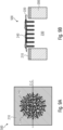
- Figure 5C shows the resulting device, namely a micromechanical environmental barrier chip 500 comprising a microstructured micromechanical environmental barrier structure 220 suspended over a through hole or cavity 230 formed in a substrate 200.
- a micromechanical environmental barrier chip 500 comprising a microstructured micromechanical environmental barrier structure 220 suspended over a through hole or cavity 230 formed in a substrate 200.
- Nanofibers 240 may be deposited on the fabricated micromechanical environmental barrier chip 500, and in particular on the environmental barrier structure 220.
- the nanofibers 240 may consist of, or may comprise, different polymers, e.g., polyvinylidene fluoride (PVDF), polyacrylonitrile (PAN), polyvinyl chloride (PVC), polytetrafluoroethylene (PTFE), polyethylene (PE), and polyaniline (PANI).
- PVDF polyvinylidene fluoride
- PAN polyacrylonitrile
- PVC polyvinyl chloride
- PTFE polytetrafluoroethylene
- PE polyethylene
- PANI polyaniline
- the nanofibers 240 may be deposited by using electrospinning techniques.
- electrospinning techniques including needleless electrospinning, multi-jet electrospinning, cylindrical porous hollow tube electrospinning, bubble electrospinning, coaxial electrospinning, melt electrospinning, force-spinning, flash-spinning, self-bundling electrospinning, nanospider electrospinning, and charge injection electrospinning.
- electrospun nanofibers 240 may possess superhydrophobic characteristics and may provide a self-cleaning effect (lotus effect).
- Surface chemistry modification by organic self-assembled monolayers (SAMs), stearic acid-based modifiers, and nanoparticles (e.g., Ag, SiO 2 , and TiO 2 ) can be carried out to further lower the surface energy of the roughened nanofiber surfaces resulting in improved hydrophobicity.
- the SAMs may consist of or comprise fluoroalkylsilanes (FAS), perfluorodecyltrichlorosilane (FDTS), and methyltrimethoxysilane (MTMS).
- embodiments of the herein described innovative method may comprise a step of applying a surface chemistry modification to the applied nanofibers 240 by depositing at least one of
- the organic self-assembled monolayers may comprise, or may consist of, at least one of:
- the innovative micromechanical environmental barrier chip 500 may be used with micromechanical MEMS-based acoustic components, like MEMS microphones, MEMS speaker or the like.
- micromechanical MEMS-based acoustic components like MEMS microphones, MEMS speaker or the like.
- SNR Signal-to-Noise Ratio
- nanofibers 240 may be deposited allowing high airflow through the holes or pores of the micromechanical environmental barrier structure 220.
- an adhesion promoter as a middle layer between the applied nanofibers 240 and the micromechanical environmental barrier structure 220, increasing the surface roughness of the micromechanical environmental barrier structure 220, or a three-dimensional (3D) modification of the micromechanical environmental barrier structure 220.
- the nanofibers 240 may be applied onto the micromechanical environmental barrier structure 220 such that the nanofibers 240 combine to form an air permeable nanofibrous membrane structure. Therefore, the nanofibers 240 can support the environmental barrier structure 220 in its functionality, i.e. to let a predetermined amount of air pass while preventing a predetermined amount of at least one of moisture, liquids, oil and solid environmental particles from passing.
- the nanofibers 240 may be applied on either one of a first side 251 (top) or a second side 252 (bottom) of the micromechanical environmental barrier structure 220. Alternatively, the nanofibers 240 may be applied on both the first and second sides 251, 252 (top and bottom) of the micromechanical environmental barrier structure 220.
- the innovative method may allow to manufacture a MEMS-based mesh chip 500 integrated with a nanofiber membrane 240.
- the micromechanical environmental barrier chip 500 may comprise a substrate 200 (e.g. a silicon substrate), having a through hole 230 formed therein.
- the through hole 230 extending between the first substrate surface 201 and the opposite second substrate surface 202 completely through the substrate 200.
- An additional material layer 210 e.g. an etch stop layer comprising TEOS
- the through hole 230 may also extend through this material layer 210.
- a micromechanical environmental barrier structure 220 e.g.
- a MEMS-based mesh or membrane may be arranged at the first substrate surface 201, in particular at the additional material layer 210.
- the micromechanical environmental barrier structure 220 may be suspended over the through hole 230.
- Nanofibers 240 may be applied onto the micromechanical environmental barrier structure 220, e.g. by means of electrospinning techniques. The applied nanofibers 240 may combine to form a nanofibrous mat or a nanofiber membrane.
- nanofibers 240 may comprise less optimal adhesion characteristics for adhering the nanofibers 240 to the environmental barrier structure 220 and/or to the substrate 200. This may be an issue if an air flow with high air pressure passes through the MEMS-based mesh chip 500. If the nanofibers 240 are not properly fixed to the environmental barrier structure 220, then they may be swept away. To keep the nanofibers 240 stable on their position after deposition (i.e., to increase the stability of the nanofibers 240 at higher air pressure), one or more additional layers having a geometrical shape comprising, for instance, a frame or a ring structure, may optionally be applied on top of the nanofibers 240. Hence, this optional additional layer(s) (e.g., metal) can hold or fix the nanofibers 240.
- this optional additional layer(s) e.g., metal
- Figures 8A to 9B show some possible implementations and exemplary embodiments of an environmental barrier chip 500 with an integrated environmental barrier structure 220 and an additional nanofiber membrane 240.
- Figure 8B shows a cross-sectional view across the sectional line B-B shown in Figure 8A .
- Figure 9B shows a cross-sectional view across the sectional line C-C shown in Figure 9A .
- the nanofibers 240 may be applied randomly crosswise over the environmental barrier structure 220.
- the nanofibers 240 may be applied in multiple passes creating a nanofiber structure (e.g. membrane or mat) comprising multiple layers of stacked nanofibers 240 being arranged one atop the other, as shown in Figures 8B and 9B .
- the nanofibers 240 may extend over the horizontal ribs 222 ( Fig. 8B ) which form the mesh of the environmental barrier structure 220, and the nanofibers 240 may extend over the holes between the horizontal ribs 222 ( Fig. 9B ).
- the whole process as described herein may be performed at wafer-level, wherein the substrate 200 may be a wafer from which a plurality of the above described micromechanical environmental barrier chips 500 can be produced.
- the innovative method may further comprise a step of singulating (e.g., by dicing) said plurality of micromechanical environmental barrier chips 500 from the wafer.
- an innovative device separation concept will be described herein by introducing thin microplates or microbeams between the single environmental barrier chips 500.
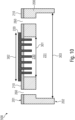
- a non-limiting embodiment is depicted in Figure 10 .
- the material layer 210 underneath the environmental barrier structure 220 may be removed, as discussed above.
- the above described cavity 230 is shown, which will be referred to as a first cavity in the following.
- Said first cavity 230 may comprise a lateral extension 301 that is equal to or smaller than the outer contour 302 (e.g. outer diameter) of the micromechanical environmental barrier structure 220.
- the lateral extension is to be measured in-plane of the chip 500, i.e. orthogonally to the substrate thickness between the first and second substrate surfaces 201, 202.
- the step of applying the anisotropic etching process may further comprise an anisotropic etching step for anisotropically etching from the second substrate surface 202 towards the first substrate surface 201 so as to create a second cavity 231 in the substrate 200.
- the second cavity 231 may comprise a larger lateral extension 303 than the first cavity 230.
- the step of applying the anisotropic etching process may comprise a further anisotropic etching step for anisotropically etching a plurality of discontinuous trenches 260 into the substrate 200, and optionally also into the material layer 210.
- the plurality of discontinuous trenches 260 may vertically extend between the first substrate surface 201 and the second cavity 231. Additionally or alternatively, the plurality of discontinuous trenches 260 may laterally surround the micromechanical environmental barrier structure 220.
- the term 'discontinuous' here means that the trenches 260 are not completely formed all around the environmental barrier structure 220, i.e., they are not fully surrounding the environmental barrier structure 220. Instead, some portions of substrate material may be left in between, such that the trenches 260 are separated from each other. These remaining portions of substrate material will form microbeams that hold the environmental barrier chip 500 on the substrate 200 prior to singulating it (e.g., by dicing). This shall be further explained with reference to Figure 11 .
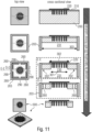
- Figure 11 shows, from top to bottom, method steps for creating the above mentioned micro beams.
- the left hand side shows top views of the environmental barrier chip 500, while cross sectional views are shown on the right.
- the unprocessed substrate 200 is shown.
- the additional material layer 210 e.g. TEOS
- the environmental barrier structure 220 is arranged on top of the material layer 210.
- the uppermost picture row shows the fabrication of the micromechanical environmental barrier structure 220 by processing a main layer using surface MEMS micromachining methods.
- the environmental barrier structure 220 may be created as either a mesh or a membrane.
- a mesh is shown as an example.
- nanofibers may be applied onto the environmental barrier structure 220.
- the second picture row shows a method step of applying the anisotropic etching process which may comprise applying an anisotropic etching step, e.g. Reactive Ion Etching (RIE) using a Bosch etching process, for anisotropically etching a cavity 231 into the substrate 200.
- This cavity 231 may correspond to the above described second cavity 231.
- the lateral / circumferential remaining portions 203 of the substrate 200, where the second cavity 231 was not formed may be thicker (thickness measured between first (top) surface and second (bottom) surface of the unprocessed substrate 200 in the uppermost picture row) than the rest of the substrate 200, where the second cavity 231 was formed.
- the substrate 200 is thinned in an area, where the cavity 231 is formed.
- the second cavity 231 may comprise a larger lateral extension 303 than the first cavity 230, that may be formed in a next method step.
- the third picture row shows a top view of the environmental barrier chip 500 on the left, and a cross-sectional view along the cross sectional line E-E on the right.
- the fourth picture row shows a cross-sectional view along the cross sectional line D-D.
- a further cavity 230 is etched into the substrate 200 by applying an anisotropic etching step, e.g. Reactive Ion Etching (RIE) using a Bosch etching process.
- This further cavity 230 may correspond to the above described first cavity 230 that is etched from the second substrate surface 202 up to the material layer 210, e.g. TEOS as an etch stop layer. Since the substrate 200 is thinned in this area, as mentioned above, the second substrate surface 202 may be the substrate surface of the thinned substrate 200, as shown in the picture.
- RIE Reactive Ion Etching
- the first cavity 230 may be etched into the thinned substrate 200, from the second surface 202 of the thinned substrate 200 up to the material layer 210.
- the first cavity 230 may comprise a lateral extension 301 that is equal to or smaller than the outer contour 302 (e.g., outer diameter) of the micromechanical environmental barrier structure 220.
- the anisotropic etching process may further comprise a step of anisotropically etching a plurality of discontinuous trenches 260 into the thinned substrate 200.
- This step may be performed at the same time as the above described step of creating the first cavity 230, i.e., the first cavity 230 and the discontinuous trenches 260 may be created in one and the same step of the anisotropic etching process.
- the plurality of discontinuous trenches 260 may vertically extend between the first substrate surface 201 and the second cavity 231. That is, the discontinuous trenches 260 may be etched into the thinned portions of the substrate 200.
- the plurality of discontinuous trenches 260 may laterally surround the micromechanical environmental barrier structure 220.
- the term 'discontinuous' here means that the trenches 260 are not completely formed all around the environmental barrier structure 220, i.e. they are not fully surrounding the environmental barrier structure 220. Instead, some portions of substrate material 290 may be left in between, such that the trenches 260 are separated from each other. These remaining portions 290 of substrate material will form micro beams 290 that hold the environmental barrier chip 500 on the substrate 200 prior to singulating it, e.g. by dicing.
- the step of etching the plurality of discontinuous trenches 260 may comprise a step of leaving portions 290 of substrate material (optionally with the material layer 210 on top) inside the plurality of discontinuous trenches 260, such that these portions 290 form micro beams 290 which structurally connect the micromechanical environmental barrier chip 500 on one side of the plurality of discontinuous trenches 260 with the substrate 200 (e.g., a wafer) on an opposite other side of the plurality of discontinuous trenches 260.
- the micro beams 290 may comprise the same thickness as the thinned substrate 200. Accordingly, the remaining thicker lateral/circumferential portions 203 (cross-hatched lines) of the substrate 200 may provide a frame structure at which the thinned substrate 200 may be suspended by means of the micro beams 290. Since the micro beams 290 may comprise the same thickness as the thinned substrate 200, the micro beams 290 can easily be broken / ruptured in order to singulate a single environmental barrier chip 500 from the substrate 200 during a pick-and-place process, in particular in case the substrate 200 is provided as a wafer. The last picture row (from top) shows a singulated environmental barrier chip 500.
- the plurality of discontinuous trenches 260 may define the lateral size of the final singulated micromechanical environmental barrier chip 500.
- the above described etching steps may deem to define the final chip size after singulating the chip 500, as well as to create the thin micro beams 290 for separating the environmental barrier chip 500.
- the separation of the environmental barrier chip 500 from the wafer 200 may be done by using pick-and-place joining techniques.
- a MEMS environmental barrier chip 500 on a thinned substrate 200 can be realized.
- a double Bosch etching process may be applied for creating the above described first and second cavities 230, 231. This method may be beneficial to avoid high SNR loss affected by a reduced back volume inside a lid of a MEMS microphone system, for example.
- a typical thickness of an initial unprocessed substrate 200, that may be used to create an environmental barrier structure 220 as described herein, may be between 200 ⁇ m and 500 ⁇ m, and preferably between 300 ⁇ m and 400 ⁇ m.
- the final environmental barrier chip 500 may comprise a thickness (i.e. height) between 20 ⁇ m and 150 ⁇ m, and preferably between 30 ⁇ m and 60 ⁇ m, depending on the used reactive ion etching (RIE) process parameters, especially the etching duration.
- RIE reactive ion etching
- the unprocessed initial substrate 200 (prior to applying the anisotropic etching process) may comprise a thickness between 200 ⁇ m and 500 ⁇ m.
- the second cavity 231 may be formed such that a thinned remaining portion of the substrate 200 results that comprises a thickness between 20 ⁇ m to 150 ⁇ m and which defines the final thickness of the environmental barrier chip 500.
- any of the material layer 210 underneath the environmental barrier structure 220 may be removed, as discussed above.
- the etching steps for forming the first and second cavities 230, 231, respectively, may be swapped regarding their temporal execution, i.e. the smaller first cavity 230 may be created first, before creating the larger second cavity 231 afterwards.
- micro beams 290 may be created resulting in optimized device breaking performance during the pick-and-place process. These may include but are not limited to rectangular micro beams 290 ( Figure 12B ), trapezoidal beams ( Figure 12A ), round-edged trapezoidal micro beams 290 ( Figure 12D ), and perforation-integrated beams ( Figure 12C ). In case of trapezoidal micro beams, the smaller region is located at the inner part close to the active area of the membrane.
- the micro beams 290 are located approximately in the center of each of the four lateral sides of the environmental barrier chip 500. Additionally or alternatively, one or more micro beams 290 may be located at different positions, e.g., at one or more corner regions of the environmental barrier chip 500.
- micro beams 290 may comprise at least one of the following geometrical shapes:
- Figures 12A to 12D show different designs of micro beams 290 for breaking the device 500 from the wafer 200.
- the micro beams 290 may be created in various shapes to optimize the separation process.
- Figure 12E shows a cross-sectional view along line F-F in Figure 12A .
- Figure 12F shows a cross-sectional view along line G-G in Figure 12A .
- the rectangle 400 drawn in dashed lines marks the micro beams 290 ( Figure 12E ) and the trenches 260 ( Figure 12F ), respectively, in the thinned substrate 200.
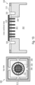
- Figure 13 shows a further embodiment of an environmental barrier chip 500, wherein a top view of the environmental barrier chip 500 is shown on the left side, while a cross-sectional view of the environmental barrier chip 500 along the cross-section line H-H is depicted on the right.
- Additional stopping structures 330 may be created on the edge of the mechanical supporting substrate 200 to avoid adhesive (glue) to reach the environmental barrier structure 220, e.g., an active membrane area, during the joining process.
- Said additional stopping structures 330 may be provided as a continuous trench, as exemplarily depicted.
- the innovative method may comprise a step of etching a continuous trench 330 into the substrate 220 (and optionally into the material layer 210).
- the continuous trench 330 may laterally surround the micromechanical environmental barrier structure 220.
- the trench 330 may be discontinuous.
- the trench 330 may preferably comprise a circular shape, while other geometrical shapes may be possible.
- stopping structure 330 is depicted in combination with the above discussed micro beams 290, the stopping structure 330 for trapping the adhesive may also be provided in each of the other embodiments that may not necessarily comprise the micro beams 290 and/or the discontinuous trenches 260.
- the stopping structure 330 (e.g. trench) may be located laterally between the micromechanical environmental barrier structure 220 and the micro beams 290, as shown in the top view of Figure 13 .
- the stopping structure 330 may comprise a circular shape.
- the method may comprise creating a circular trench 330 for stopping the bleeding of any applied adhesive (e.g., glue, solder paste, or the like) during a joining process between the environmental barrier chip 500 and a further acoustic component, such as a MEMS microphone chip.
- a further acoustic component such as a MEMS microphone chip.
- This protecting trench concept is an additional optional feature for the joining technique that involves the environmental barrier chip 500 placed inside a lid of a sound component package, such as a MEMS microphone package, in particular if the environmental barrier chip 500 may be placed underneath the MEMS microphone chip.
- the whole process as described herein may be performed at wafer-level, wherein the substrate 200 may be a wafer from which a plurality of the above described micromechanical environmental barrier chips 500 may be singulated.
- the innovative method may further comprise a step of singulating (e.g. by dicing) said plurality of micromechanical environmental barrier chips 500 from the wafer 200.
- the micromechanical environmental barrier chips 500 may be fabricated using wafer-level front-end processing.
- the innovative micromechanical environmental barrier chip 500 may be integrated to the frontend chip, instead of manufacturing environmental barriers as individual devices.
- an acoustic component e.g. a MEMS-microphone
- This may provide for a low-cost packaging solution for microphones with higher robustness against ingress of environmental solid, gaseous and/or moist particles.
- the above described versatile device separation concept may be applied not only for passive environmental barrier structures 220 (e.g. membrane, mesh, nanofiber membrane-integrated mesh chips), but also for active MEMS devices like microphones, pressure sensors, and others.
- the created environmental barrier chip 500 based on this separation method can be mounted into a microphone package in different architectures, as will be explained in more detail with reference to Figures 14A to 14E .
- the created environmental barrier chip 500 may comprise a single environmental barrier structure 220 (e.g., environmental barrier mesh only, environmental barrier membrane only, or environmental barrier nanofibers only) or joint environmental barrier elements (e.g. a nanofiber membrane-integrated mesh chip or environmental barrier membrane-stacked environmental barrier mesh chip).
- FIGS 14A to 14E show some non-limiting examples of packaging concepts for the micromechanical environmental barrier chip 500 according to the herein described innovative principle.
- the package 600 may comprise a carrier substrate 601, e.g. a PCB, comprising a sound port opening 602.
- the package 600 may further comprise a cover or lid 603 being arranged on the substrate 601.
- the lid 603 provides a cavity 604 inside of which different electrical and/or electronic components may be arranged.
- a MEMS microphone chip 605 may be arranged inside the cavity 604. Additionally, the herein described innovative micromechanical environmental barrier chip 500 may be arranged inside the cavity 604. Furthermore, a circuitry 606 may be arranged inside the cavity 604. The circuitry 606 may be provided as an integrated circuit (IC), for instance as an ASIC (Application Specific Integrated Circuit). The circuitry 606 may be electrically connected to the MEMS microphone chip 605, for example by means of bond wires 607.
- IC integrated circuit
- ASIC Application Specific Integrated Circuit
- the environmental barrier chip 500 may be arranged directly opposite the sound port 602 such that the environmental barrier chip 500 is in direct fluid communication with the sound port 602.
- environmental solid, gaseous and/or moist particles may be prevented from entering the cavity 604 of the package 600.
- the MEMS microphone chip 605 may be stacked directly atop the environmental barrier chip 500.
- the environmental barrier chip 500 prevents environmental solid, gaseous and/or moist particles from reaching (and possibly destroying) the sensitive membrane of the MEMS microphone 605.
- the environmental barrier chip 500 may be attached to the carrier substrate 601 by means of adhesive, e.g. glue. Additionally or alternatively, the MEMS microphone chip 605 may be attached to the environmental barrier chip 500 by means of an adhesive, e.g. glue.
- Figure 14A shows an exemplary packaging concept in which the environmental barrier chip 500 comprises an environmental barrier structure 220 formed as a micro machined mesh, in combination with nanofibers 240, as described with reference to Figures 6A to 7A .
- Figure 14A shows a nanofiber-integrated environmental barrier mesh chip 500 arranged inside the package 600.
- Figure 14B shows a further exemplary packaging concept in which the environmental barrier chip 500 comprises an environmental barrier structure 220 formed as a micro machined mesh without nanofibers, as described with reference to Figures 2A to 5C .
- Figure 14B shows an environmental barrier mesh chip 500 without nanofibers arranged inside the package 600.
- Figure 14C shows a further exemplary packaging concept in which the environmental barrier chip 500 comprises an environmental barrier structure 220 formed as a nanofibrous membrane or nanofibrous mat only, which may be fabricated from deposited nanofibers 240. It is to be mentioned that each and every embodiment of the environmental barrier structure 220 according to the herein described innovative principle may be formed as a nanofibrous membrane or nanofibrous mat only, which may be fabricated from deposited nanofibers 240, i.e. without any micromachined mesh or membrane.
- Figure 14C shows an environmental barrier nanofiber membrane chip 500 arranged inside the package 600.
- Figure 14D shows a further exemplary packaging concept in which the environmental barrier chip 500 comprises an environmental barrier structure 220 formed as a membrane. It is to be mentioned that each and every embodiment of the environmental barrier structure 220 according to the herein described innovative principle may be formed as a membrane instead of a micromachined mesh.
- the membrane 220 may be plane or structured with high compliance. Nanofibers may optionally be deposited thereon.
- Figure 14D shows an environmental barrier membrane chip 500 with a membrane made from material other than nanofibers arranged inside the package 600.
- Figure 14E shows a further exemplary packaging concept in which two environmental barrier chips 501, 502 may be stacked one atop the other.
- a first environmental barrier chip 501 may comprise a microstructured mesh (with or without nanofibers deposited thereon).
- a second environmental barrier chip 502 may comprise a membrane (with or without nanofibers deposited thereon).
- One of the first and second environmental barrier chips 501, 502 may be arranged on the carrier substrate 601 opposite the sound port 602.
- the other one of the first and second environmental barrier chips 501, 502 may be stacked atop the bottom one.
- the MEMS microphone chip 605 may be stacked atop the first and second environmental barrier chips 501, 502.
- Figure 14E shows a membrane-stacked mesh chip 500 arranged inside the package 600.
- the innovative method may further comprise a step of packaging the micromechanical environmental barrier chip 500 by mounting the micromechanical environmental barrier chip 500 together with a MEMS microphone chip 605 onto a carrier substrate 601, and arranging a package lid 603 on the carrier substrate 601, such that the package lid 603 covers and encloses the micromechanical environmental barrier chip 500 and the MEMS microphone chip 605.
- the micromechanical environmental barrier chip 500 may be directly attached to the carrier substrate 601, wherein the MEMS microphone chip 605 is directly attached on top of the micromechanical environmental barrier chip 500, thereby forming a chip stack in which the micromechanical environmental barrier chip 500 is positioned between the MEMS microphone chip 605 and the carrier substrate 601.
- the carrier substrate 601 may comprise a sound port opening 602, wherein the micromechanical environmental barrier chip 500 faces the sound port opening 602, such that the environmental barrier chip 500 is in fluid communication with the sound port opening 602.
- micromechanical environmental barrier chip 500 and the MEMS microphone chip 605 may be provided as two separate discrete components.
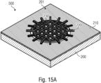
- Figure 15A shows a schematic perspective view of an environmental barrier chip 500 with an environmental barrier structure 220 attached to the first substrate surface 201.
- Figure 15B shows a picture taken with a scanning electron microscope, said picture showing the upper surface (i.e. first substrate surface 201) of the environmental barrier chip 500, wherein the environmental barrier structure 220 is provided as a micromachined mesh with square grids 223.
- Each of the square grids 223 may comprise a square grid size of x ⁇ m (i.e. the length is x ⁇ m, and the width is also x ⁇ m).
- the environmental barrier structure 220 is arranged above the first cavity 230.
- the cavity 230 may comprise a size of y ⁇ m. In case of a circular cavity 230, the size is defined as the diameter of the cavity 230.
- Figure 15C shows the correlation between the square grid size and the SNR loss in dB.
- the numbers are only for illustrating purposes and shall not be construed as being limiting in any way.
- the smaller the square grid size the higher the SNR loss. In other words, a smaller grid size leads to a higher SNR loss.
- the grey shaded box shows an optimal range, indicating that a square grid size of 18 ⁇ m or more is desirable.
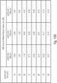
- Figure 15D shows the correlation between the square grid size and the cavity size.
- the grey-shaded rows and columns indicate combinations that worked well.
- different cavity sizes resulted in similar trends with varied SNR loss values, in which a grid size of 10 ⁇ m can be excluded from the design because of too high SNR loss.
- a grid size of 20 ⁇ m in combination with a cavity size of 800 ⁇ m may be excluded.
- the square grid size of an environmental barrier structure 220 shall be 20 ⁇ m or more in order to provide a good SNR while efficiently preventing environmental solid, gaseous and/or moist particles from passing the environmental barrier structure 220.
- the herein described innovative concept provides for manufacturing and integration methods for MEMS-based environmental barriers 220. It further provides for a device separation concept for packaging purposes.
- aspects have been described in the context of an apparatus, it is clear that these aspects also represent a description of the corresponding method, where a block or device corresponds to a method step or a feature of a method step. Analogously, aspects described in the context of a method step also represent a description of a corresponding block or item or feature of a corresponding apparatus.
Landscapes
- Engineering & Computer Science (AREA)
- Microelectronics & Electronic Packaging (AREA)
- Computer Hardware Design (AREA)
- Manufacturing & Machinery (AREA)
- Toxicology (AREA)
- General Health & Medical Sciences (AREA)
- Health & Medical Sciences (AREA)
- Physics & Mathematics (AREA)
- Chemical & Material Sciences (AREA)
- Nanotechnology (AREA)
- Mechanical Engineering (AREA)
- Signal Processing (AREA)
- Crystallography & Structural Chemistry (AREA)
- General Physics & Mathematics (AREA)
- Condensed Matter Physics & Semiconductors (AREA)
- Acoustics & Sound (AREA)
- Micromachines (AREA)
Abstract
Description
- Embodiments of the present disclosure relate to a micromechanical environmental barrier chip for providing a protection for MEMS microphones or MEMS speakers against ingress of environmental solid, gaseous and/or moist particles. Further embodiments relate to a manufacturing method thereof.
- Despite their wide employment in several acoustic applications like smartphones, true wireless (TWS) earphones, etc., current microelectromechanical system (MEMS)-based microphones are prone to influences from dust particles, moisture, and other physical or chemical objects, which consequently result in a lower robustness and shortened lifetime of the devices.
- Currently available solutions from microphone manufacturers rely on external and large environmental barriers (EBs) that are placed far away from the microphone chips, leading to high production cost, large package size, low acoustic performance, and limited usage for applications.
- Thus, it would be desirable to provide a microstructured environmental barrier for MEMS-based acoustic elements, said environmental barrier comprising a small form factor while providing reliable and robust protection against ingress of environmental solid, gaseous and/or moist particles. It would further be desirable to provide a manufacturing method thereof that enables a reduction in production costs.
- These goals can be achieved with a method for manufacturing a micromechanical environmental barrier chip according to the herein described innovative principle. Said method comprises a step of providing a substrate having a first surface and an opposite second surface, a step of depositing a material layer onto the first surface of the substrate, the material layer having a different etch rate than the substrate, and a step of creating a microstructured micromechanical environmental barrier structure on top of the material layer by applying a microstructuring process. The method further comprises a step of applying an anisotropic etching process comprising at least one etching step for anisotropically etching from the second surface towards the first surface of the substrate so as to create at least a first cavity underneath the micromechanical environmental barrier structure, the cavity extending between the second surface and the material layer. The method further comprises a step of removing the material layer residing inside the cavity in order to expose the environmental barrier structure.
- In the following, embodiments of the present disclosure are described in more detail with reference to the figures, in which
- Fig. 1
- shows a schematic block diagram of a method for manufacturing a micromechanical environmental barrier chip according to an embodiment,
- Figs. 2A-2C
- show a method step by means of a top view, a cross-sectional view and a perspective view, respectively, of an unprocessed substrate,
- Figs. 3A-3C
- show a further method step of applying a material layer on the substrate by means of a top view, a cross-sectional view and a perspective view, respectively, of the substrate,
- Figs. 4A-4C
- show a further method step of creating an environmental barrier structure on top of the material layer by means of a top view, a cross-sectional view and a perspective view, respectively, of the substrate,
- Figs. 5A-5C
- show a further method step of creating a cavity in the substrate by means of a top view, a cross-sectional view and a perspective view, respectively, of the substrate,
- Figs. 6A-6C
- show a further method step of applying nanofibers onto the environmental barrier structure by means of a top view, a cross-sectional view and a perspective view, respectively, of the substrate,
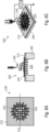
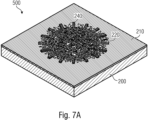
- Fig. 7A
- shows a perspective view of an environmental barrier chip with nanofibers applied thereon,
- Fig. 7B
- shows an exploded view of the environmental barrier chip of
Figure 7A , - Fig. 8A
- shows a top view onto the environmental barrier chip of
Figure 7A , - Fig. 8B
- shows a cross-sectional view along the cross-sectional line B-B in
Figure 8A , - Fig. 9A
- shows a top view onto the environmental barrier chip of
Figure 7A , - Fig. 9B
- shows a cross-sectional view along the cross-sectional line C-C in
Figure 9A , - Fig. 10
- shows a cross-sectional view of an environmental barrier chip according to a further embodiment,
- Fig. 11
- shows a sequence of method steps for creating the environmental barrier chip of
Figure 10 , - Figs. 12A-12D
- show top views of an environmental barrier chip with micro beams according to embodiments,
- Fig. 12E
- shows a cross-sectional view of the environmental barrier chip of
Figure 12A along the cross-sectional line F-F, - Fig. 12F
- shows a cross-sectional view of the environmental barrier chip of
Figure 12A along the cross-sectional line G-G, - Fig. 13
- shows a cross-sectional view and a top view of an environmental barrier chip according to an embodiment,
- Figs. 14A-14E
- show different packaging concepts,
- Fig. 15A
- shows a perspective view of an environmental barrier chip according to an embodiment,
- Fig. 15B
- shows a picture of the environmental barrier chip taken with a raster electron microscope,
- Fig. 15C
- shows a graphical illustration of a simulation for comparing square grid size against SNR loss, and
- Fig. 15D
- shows a further graphical illustration of a simulation for comparing square grid size against SNR loss.
- Equal or equivalent elements or elements with equal or equivalent functionality are denoted in the following description by equal or equivalent reference numerals.
- Method steps which are depicted by means of a block diagram and which are described with reference to said block diagram may also be executed in an order different from the depicted and/or described order. Furthermore, method steps concerning a particular feature of a device may be replaceable with said feature of said device, and the other way around.
-
Figure 1 shows a schematic block diagram of the herein described innovative method according to an embodiment. The single method steps may be executed in a different order than depicted and described in the following. - In
block 101, a substrate may be provided, said substrate having a first surface and an opposite second surface. - In block 102 a material layer may be deposited onto the first surface of the substrate, the material layer having a different etch characteristic than the substrate. An etch characteristic may include a certain selectivity. The selectivity describes an etch ratio between two different materials. For example, if the selectivity is 2:1, then a first material will be etched/removed two times faster than a second material, when applying the same etching process for the same time duration on both materials.
- In block 103 a microstructured micromechanical environmental barrier structure may be provided on top of the material layer by applying a microstructuring process.
- In
block 104 an anisotropic etching process may be performed comprising at least one etching step for anisotropically etching through the substrate (e.g. from the second surface towards the first surface of the substrate) until reaching the material layer so as to create at least a first cavity opposite (e.g. underneath) the micromechanical environmental barrier structure, the cavity extending between the second surface and the material layer. - In
block 105 any of the material layer that resides inside the cavity may be removed in order to expose the environmental barrier structure. -
Figures 2A to 5C show a structural description of the innovative method.Figures 2A ,3A ,4A and5A show a top view onto thesubstrate 200 to be processed.Figures 2B ,3B ,4B and5B show a cross-sectional view along the section line A-A.Figures 2C ,3C ,4C and5C show a perspective view of thesubstrate 200. - Starting with
Figures 2A to 2C , asubstrate 200 is depicted, thesubstrate 200 having afirst surface 201 and an oppositesecond surface 202. Thesubstrate 200 may consist of, or comprise, a semiconductor material, such as silicon, for example. Alternatively, thesubstrate 200 may consist of, or comprise, glass, (poly-)imide, plastics or the like. Thesubstrate 200 may be flexible or rigid. -
Figures 3A to 3C show a further method step. Amaterial layer 210 may be deposited onto thefirst surface 201 of thesubstrate 200. Thematerial layer 210 may be deposited completely over the entirefirst surface 201. Thematerial layer 210 may comprise a different etch characteristic than thesubstrate 200. For example, thematerial layer 210 and thesubstrate 200 may comprise a high selectivity for one and the same etchant. The selectivity describes the etch ratio between thematerial layer 210 and thesubstrate 200. For example, thesubstrate 200 may be etched/removed significantly faster than thematerial layer 210. In some embodiments, thesubstrate 210 may be completely removed while thematerial layer 210 is not noticeably etched/removed. - Accordingly, as will be explained in more detail below, the
material layer 210 may serve the purpose of an etch stop layer. For example, thematerial layer 210 may consist of or comprise tetraethyl orthosilicate, formally named tetraethoxysilane (TEOS), or other oxide (e.g., thermal silicon dioxides - SiO2 -, atomic layer deposited oxide) and nitride (e.g., silicon nitride) materials. These materials have an insulating characteristic. For example, the etch rate between TEOS (as the material layer 210) and silicon (substrate 200) is about 1:100, i.e., silicon is etched/removed a hundred times faster than TEOS. -
Figures 4A to 4C show a further method step. A microstructured micromechanicalenvironmental barrier structure 220 may be created on top of thematerial layer 210. The micromechanicalenvironmental barrier structure 220 may be formed by applying a microstructuring process, e.g., a surface MEMS micromachining process. The micromechanicalenvironmental barrier structure 220 may be provided as an air permeable mesh, as depicted, or as a perforated air permeable membrane. - The micromechanical
environmental barrier structure 220 may comprise a circular or rectangular shape, while other geometrical shapes are possible. The micromechanicalenvironmental barrier structure 220 may comprise vertically extendingrib structures 221 that may extend through thematerial layer 210 and penetrate into thesubstrate 200, as shown inFigure 4B . Therib structures 210 may be arranged in a cross-wise manner thereby creating a mesh structure. - The micromechanical
environmental barrier structure 220 may be fabricated using wafer-level front-end processing. A main layer of the micromechanicalenvironmental barrier structure 220 may comprise various materials used in front-end semiconductor processing, which include but are not limited to silicon, nitride, stacked silicon/nitride, and polymeric materials, e.g., polyimide, poly(methyl methacrylate) (PMMA), polydimethylsiloxane (PDMS), SU-8, and benzocyclobutene (BCB). The micromechanicalenvironmental barrier structure 220 may be rigid and may provide sufficient large hole openings (e.g., 10 µm to 40 µm) to avoid high loss of signal-to-noise ratio (SNR) and sensitivity. -
Figures 5A to 5C show a further method step. An anisotropic etching process, e.g. Reactive Ion Etching (RIE) using a Bosch etching process, may be applied comprising at least one etching step for anisotropically etching from thesecond surface 202 towards thefirst surface 201 of thesubstrate 200 so as to create at least afirst cavity 230 underneath (i.e. opposite to) the micromechanicalenvironmental barrier structure 220. Thecavity 230 may extend completely through thesubstrate 200. Therefore, thecavity 230 may also be referred to as an opening or a through hole. - As mentioned above, the
material layer 210 may serve as an etch stop layer. Accordingly, thesubstrate 200 may be etched until the etchant reaches thematerial layer 210. Even though not explicitly shown inFigures 5A to 5C , some of thematerial layer 210 may remain underneath the micromechanicalenvironmental barrier structure 220, i.e. it may remain between the micromechanicalenvironmental barrier structure 220 and thecavity 230. -
Figures 5A to 5C show a method step, in which thematerial layer 210 underneath the micromechanicalenvironmental barrier structure 220 was already removed such that the micromechanicalenvironmental barrier structure 220 is already exposed. However, in some embodiments only those portions of thematerial layer 210 being located underneath the micromechanicalenvironmental barrier structure 220 may be removed, as shown inFigures 5A to 5C , while the rest of the depositedmaterial layer 210 may remain on thefirst surface 201 of thesubstrate 200. - After removal of the
material layer 210 underneath the micromechanicalenvironmental barrier structure 220, as shown inFigure 5B , the micromechanicalenvironmental barrier structure 220 is exposed, i.e. it is in direct fluid contact with thecavity 230. Accordingly, fluids, and in particular gaseous fluids like ambient air, may flow through thecavity 230 and pass the micromechanicalenvironmental barrier structure 220. - The micromechanical
environmental barrier structure 220 may be configured to let a predetermined amount of air pass while preventing a predetermined amount of at least one of moisture, liquids, oil and solid environmental particles from passing. -
Figure 5C shows the resulting device, namely a micromechanicalenvironmental barrier chip 500 comprising a microstructured micromechanicalenvironmental barrier structure 220 suspended over a through hole orcavity 230 formed in asubstrate 200. As will be explained in more detail below, the herein described innovative method allows for a very thin micromechanicalenvironmental barrier chip 500. Details shall be described somewhat later with reference toFigures 10 to 13 . - Meanwhile, reference shall be made to
Figures 6A to 6C showing further optional method steps.Nanofibers 240 may be deposited on the fabricated micromechanicalenvironmental barrier chip 500, and in particular on theenvironmental barrier structure 220. Thenanofibers 240 may consist of, or may comprise, different polymers, e.g., polyvinylidene fluoride (PVDF), polyacrylonitrile (PAN), polyvinyl chloride (PVC), polytetrafluoroethylene (PTFE), polyethylene (PE), and polyaniline (PANI). - The
nanofibers 240 may be deposited by using electrospinning techniques. Various electrospinning methods can be opted, including needleless electrospinning, multi-jet electrospinning, cylindrical porous hollow tube electrospinning, bubble electrospinning, coaxial electrospinning, melt electrospinning, force-spinning, flash-spinning, self-bundling electrospinning, nanospider electrospinning, and charge injection electrospinning. - For example,
electrospun nanofibers 240 may possess superhydrophobic characteristics and may provide a self-cleaning effect (lotus effect). Surface chemistry modification by organic self-assembled monolayers (SAMs), stearic acid-based modifiers, and nanoparticles (e.g., Ag, SiO2, and TiO2) can be carried out to further lower the surface energy of the roughened nanofiber surfaces resulting in improved hydrophobicity. The SAMs may consist of or comprise fluoroalkylsilanes (FAS), perfluorodecyltrichlorosilane (FDTS), and methyltrimethoxysilane (MTMS). - Accordingly, embodiments of the herein described innovative method may comprise a step of applying a surface chemistry modification to the applied
nanofibers 240 by depositing at least one of - organic self-assembled monolayers,
- stearic acid-based modifiers, and
- nanoparticles
- Besides the above mentioned exemplary components, the organic self-assembled monolayers may comprise, or may consist of, at least one of:
- Perfluorodecyltrichlorosilane (FDTS),
- Heptadecafluoro-1,1,2,2-tetrahydrodecyltrichlorosilane (HDFS),
- Tridecafluoro-1,1,2,2-tetrahydrooctyltrichlorosilane (FOTS),
- Octadecyltrichlorsilane (ODTS),
- Methyltrimethoxysilane (MTMS),
- Bis(trimethylsilyl)amine or hexamethyldisilazane (HMDS),
- (3-Aminopropyl)triethoxysilane (APTES),
- Dichlorodimethylsilane (DDMS),
- Octadecyltrimethoxysilane (OTMS),
- Ethyltriethoxysilane (ETES), and
- 1H,1H,2H,2H-perfluorooctyltriethoxysilane (HFOTES).
- As mentioned above, the innovative micromechanical
environmental barrier chip 500 may be used with micromechanical MEMS-based acoustic components, like MEMS microphones, MEMS speaker or the like. To maintain a high SNR (Signal-to-Noise Ratio) of said MEMS-based acoustic components, and at the same time to provide a good environmental robustness towards particles and water, only a thin layer ofnanofibers 240 may be deposited allowing high airflow through the holes or pores of the micromechanicalenvironmental barrier structure 220. - To improve the adhesion between the applied
nanofibers 240 and the micromechanicalenvironmental barrier structure 220, several strategies can be applied, e.g. insertion of an adhesion promoter as a middle layer between the appliednanofibers 240 and the micromechanicalenvironmental barrier structure 220, increasing the surface roughness of the micromechanicalenvironmental barrier structure 220, or a three-dimensional (3D) modification of the micromechanicalenvironmental barrier structure 220. - As shown in
Figures 7A and7B , thenanofibers 240 may be applied onto the micromechanicalenvironmental barrier structure 220 such that thenanofibers 240 combine to form an air permeable nanofibrous membrane structure. Therefore, thenanofibers 240 can support theenvironmental barrier structure 220 in its functionality, i.e. to let a predetermined amount of air pass while preventing a predetermined amount of at least one of moisture, liquids, oil and solid environmental particles from passing. - The
nanofibers 240 may be applied on either one of a first side 251 (top) or a second side 252 (bottom) of the micromechanicalenvironmental barrier structure 220. Alternatively, thenanofibers 240 may be applied on both the first andsecond sides 251, 252 (top and bottom) of the micromechanicalenvironmental barrier structure 220. - Accordingly, the innovative method may allow to manufacture a MEMS-based
mesh chip 500 integrated with ananofiber membrane 240. As shown inFigure 7B , the micromechanicalenvironmental barrier chip 500 may comprise a substrate 200 (e.g. a silicon substrate), having a throughhole 230 formed therein. The throughhole 230 extending between thefirst substrate surface 201 and the oppositesecond substrate surface 202 completely through thesubstrate 200. An additional material layer 210 (e.g. an etch stop layer comprising TEOS) may be deposited at thefirst substrate surface 201. In thefinal device 500, the throughhole 230 may also extend through thismaterial layer 210. A micromechanical environmental barrier structure 220 (e.g. a MEMS-based mesh or membrane) may be arranged at thefirst substrate surface 201, in particular at theadditional material layer 210. The micromechanicalenvironmental barrier structure 220 may be suspended over the throughhole 230.Nanofibers 240 may be applied onto the micromechanicalenvironmental barrier structure 220, e.g. by means of electrospinning techniques. The appliednanofibers 240 may combine to form a nanofibrous mat or a nanofiber membrane. - Some materials used for the fabrication of nanofibers 240 (e.g. some polymers) may comprise less optimal adhesion characteristics for adhering the
nanofibers 240 to theenvironmental barrier structure 220 and/or to thesubstrate 200. This may be an issue if an air flow with high air pressure passes through the MEMS-basedmesh chip 500. If thenanofibers 240 are not properly fixed to theenvironmental barrier structure 220, then they may be swept away. To keep thenanofibers 240 stable on their position after deposition (i.e., to increase the stability of thenanofibers 240 at higher air pressure), one or more additional layers having a geometrical shape comprising, for instance, a frame or a ring structure, may optionally be applied on top of thenanofibers 240. Hence, this optional additional layer(s) (e.g., metal) can hold or fix thenanofibers 240. -
Figures 8A to 9B show some possible implementations and exemplary embodiments of anenvironmental barrier chip 500 with an integratedenvironmental barrier structure 220 and anadditional nanofiber membrane 240.Figure 8B shows a cross-sectional view across the sectional line B-B shown inFigure 8A .Figure 9B shows a cross-sectional view across the sectional line C-C shown inFigure 9A . As can be seen, thenanofibers 240 may be applied randomly crosswise over theenvironmental barrier structure 220. Thenanofibers 240 may be applied in multiple passes creating a nanofiber structure (e.g. membrane or mat) comprising multiple layers ofstacked nanofibers 240 being arranged one atop the other, as shown inFigures 8B and9B . Thenanofibers 240 may extend over the horizontal ribs 222 (Fig. 8B ) which form the mesh of theenvironmental barrier structure 220, and thenanofibers 240 may extend over the holes between the horizontal ribs 222 (Fig. 9B ). - The whole process as described herein may be performed at wafer-level, wherein the
substrate 200 may be a wafer from which a plurality of the above described micromechanicalenvironmental barrier chips 500 can be produced. In this regard, the innovative method may further comprise a step of singulating (e.g., by dicing) said plurality of micromechanicalenvironmental barrier chips 500 from the wafer. - For facilitating the singulation process and enabling a pick-and-place joining method of the innovative
environmental barrier chip 500 onto a printed circuit board (PCB) used in acoustic component packaging (e.g., for MEMS microphone packages), an innovative device separation concept will be described herein by introducing thin microplates or microbeams between the single environmental barrier chips 500. - A non-limiting embodiment is depicted in
Figure 10 . Even though not explicitly shown here, thematerial layer 210 underneath theenvironmental barrier structure 220 may be removed, as discussed above. The above describedcavity 230 is shown, which will be referred to as a first cavity in the following. Saidfirst cavity 230 may comprise alateral extension 301 that is equal to or smaller than the outer contour 302 (e.g. outer diameter) of the micromechanicalenvironmental barrier structure 220. As indicated byarrows chip 500, i.e. orthogonally to the substrate thickness between the first and second substrate surfaces 201, 202. - In this embodiment, the step of applying the anisotropic etching process may further comprise an anisotropic etching step for anisotropically etching from the
second substrate surface 202 towards thefirst substrate surface 201 so as to create asecond cavity 231 in thesubstrate 200. Thesecond cavity 231 may comprise a largerlateral extension 303 than thefirst cavity 230. - The step of applying the anisotropic etching process may comprise a further anisotropic etching step for anisotropically etching a plurality of
discontinuous trenches 260 into thesubstrate 200, and optionally also into thematerial layer 210. The plurality ofdiscontinuous trenches 260 may vertically extend between thefirst substrate surface 201 and thesecond cavity 231. Additionally or alternatively, the plurality ofdiscontinuous trenches 260 may laterally surround the micromechanicalenvironmental barrier structure 220. - The term 'discontinuous' here means that the
trenches 260 are not completely formed all around theenvironmental barrier structure 220, i.e., they are not fully surrounding theenvironmental barrier structure 220. Instead, some portions of substrate material may be left in between, such that thetrenches 260 are separated from each other. These remaining portions of substrate material will form microbeams that hold theenvironmental barrier chip 500 on thesubstrate 200 prior to singulating it (e.g., by dicing). This shall be further explained with reference toFigure 11 . -
Figure 11 shows, from top to bottom, method steps for creating the above mentioned micro beams. The left hand side shows top views of theenvironmental barrier chip 500, while cross sectional views are shown on the right. - Starting from the uppermost picture row, the
unprocessed substrate 200 is shown. The additional material layer 210 (e.g. TEOS) is deposited at thefirst substrate surface 201, and theenvironmental barrier structure 220 is arranged on top of thematerial layer 210. The uppermost picture row shows the fabrication of the micromechanicalenvironmental barrier structure 220 by processing a main layer using surface MEMS micromachining methods. Here, theenvironmental barrier structure 220 may be created as either a mesh or a membrane. In this figure, a mesh is shown as an example. Optionally, nanofibers may be applied onto theenvironmental barrier structure 220. In case of a membrane, there is no grid created. Instead, small ventholes may be provided to enable airflow coming from the package sound port. - The second picture row (from top) shows a method step of applying the anisotropic etching process which may comprise applying an anisotropic etching step, e.g. Reactive Ion Etching (RIE) using a Bosch etching process, for anisotropically etching a
cavity 231 into thesubstrate 200. Thiscavity 231 may correspond to the above describedsecond cavity 231. As indicated by means of cross-hatched lines, the lateral /circumferential remaining portions 203 of thesubstrate 200, where thesecond cavity 231 was not formed, may be thicker (thickness measured between first (top) surface and second (bottom) surface of theunprocessed substrate 200 in the uppermost picture row) than the rest of thesubstrate 200, where thesecond cavity 231 was formed. In other words, thesubstrate 200 is thinned in an area, where thecavity 231 is formed. Thesecond cavity 231 may comprise a largerlateral extension 303 than thefirst cavity 230, that may be formed in a next method step. - Therefore, it shall be referred to the third and fourth picture row (from top). The third picture row shows a top view of the
environmental barrier chip 500 on the left, and a cross-sectional view along the cross sectional line E-E on the right. The fourth picture row shows a cross-sectional view along the cross sectional line D-D. - As can be seen in the third picture row (from top), a
further cavity 230 is etched into thesubstrate 200 by applying an anisotropic etching step, e.g. Reactive Ion Etching (RIE) using a Bosch etching process. Thisfurther cavity 230 may correspond to the above describedfirst cavity 230 that is etched from thesecond substrate surface 202 up to thematerial layer 210, e.g. TEOS as an etch stop layer. Since thesubstrate 200 is thinned in this area, as mentioned above, thesecond substrate surface 202 may be the substrate surface of the thinnedsubstrate 200, as shown in the picture. That is, thefirst cavity 230 may be etched into the thinnedsubstrate 200, from thesecond surface 202 of the thinnedsubstrate 200 up to thematerial layer 210. Thefirst cavity 230 may comprise alateral extension 301 that is equal to or smaller than the outer contour 302 (e.g., outer diameter) of the micromechanicalenvironmental barrier structure 220. - As can further be seen in the third and fourth picture rows (from top), the anisotropic etching process may further comprise a step of anisotropically etching a plurality of
discontinuous trenches 260 into the thinnedsubstrate 200. This step may be performed at the same time as the above described step of creating thefirst cavity 230, i.e., thefirst cavity 230 and thediscontinuous trenches 260 may be created in one and the same step of the anisotropic etching process. As can best be seen in the fourth picture row, the plurality ofdiscontinuous trenches 260 may vertically extend between thefirst substrate surface 201 and thesecond cavity 231. That is, thediscontinuous trenches 260 may be etched into the thinned portions of thesubstrate 200. As can best be seen in the top view of the third picture row, the plurality ofdiscontinuous trenches 260 may laterally surround the micromechanicalenvironmental barrier structure 220. - As mentioned above, the term 'discontinuous' here means that the
trenches 260 are not completely formed all around theenvironmental barrier structure 220, i.e. they are not fully surrounding theenvironmental barrier structure 220. Instead, some portions ofsubstrate material 290 may be left in between, such that thetrenches 260 are separated from each other. These remainingportions 290 of substrate material will formmicro beams 290 that hold theenvironmental barrier chip 500 on thesubstrate 200 prior to singulating it, e.g. by dicing. - Accordingly, the step of etching the plurality of
discontinuous trenches 260 may comprise a step of leavingportions 290 of substrate material (optionally with thematerial layer 210 on top) inside the plurality ofdiscontinuous trenches 260, such that theseportions 290 formmicro beams 290 which structurally connect the micromechanicalenvironmental barrier chip 500 on one side of the plurality ofdiscontinuous trenches 260 with the substrate 200 (e.g., a wafer) on an opposite other side of the plurality ofdiscontinuous trenches 260. - Since the
micro beams 290 are formed in the thinnedsubstrate 200, themicro beams 290 may comprise the same thickness as the thinnedsubstrate 200. Accordingly, the remaining thicker lateral/circumferential portions 203 (cross-hatched lines) of thesubstrate 200 may provide a frame structure at which the thinnedsubstrate 200 may be suspended by means of themicro beams 290. Since themicro beams 290 may comprise the same thickness as the thinnedsubstrate 200, themicro beams 290 can easily be broken / ruptured in order to singulate a singleenvironmental barrier chip 500 from thesubstrate 200 during a pick-and-place process, in particular in case thesubstrate 200 is provided as a wafer. The last picture row (from top) shows a singulatedenvironmental barrier chip 500. - Accordingly, the plurality of
discontinuous trenches 260 may define the lateral size of the final singulated micromechanicalenvironmental barrier chip 500. In other words, the above described etching steps may deem to define the final chip size after singulating thechip 500, as well as to create the thinmicro beams 290 for separating theenvironmental barrier chip 500. The separation of theenvironmental barrier chip 500 from thewafer 200 may be done by using pick-and-place joining techniques. As a final device, a MEMSenvironmental barrier chip 500 on a thinnedsubstrate 200 can be realized. - To create the thinned mechanical supporting
substrate 200, a double Bosch etching process may be applied for creating the above described first andsecond cavities unprocessed substrate 200, that may be used to create anenvironmental barrier structure 220 as described herein, may be between 200 µm and 500 µm, and preferably between 300 µm and 400 µm. Using anisotropic etching, e.g. a double Bosch etching process, the finalenvironmental barrier chip 500 may comprise a thickness (i.e. height) between 20 µm and 150 µm, and preferably between 30 µm and 60 µm, depending on the used reactive ion etching (RIE) process parameters, especially the etching duration. - Accordingly, the unprocessed initial substrate 200 (prior to applying the anisotropic etching process) may comprise a thickness between 200 µm and 500 µm. By applying the anisotropic etching process, the
second cavity 231 may be formed such that a thinned remaining portion of thesubstrate 200 results that comprises a thickness between 20 µm to 150 µm and which defines the final thickness of theenvironmental barrier chip 500. - Even though not explicitly shown in
Figure 11 , any of thematerial layer 210 underneath theenvironmental barrier structure 220 may be removed, as discussed above. Furthermore, the etching steps for forming the first andsecond cavities first cavity 230 may be created first, before creating the largersecond cavity 231 afterwards. - As shown in
Figures 12A to 12F , various designs ofmicro beams 290 may be created resulting in optimized device breaking performance during the pick-and-place process. These may include but are not limited to rectangular micro beams 290 (Figure 12B ), trapezoidal beams (Figure 12A ), round-edged trapezoidal micro beams 290 (Figure 12D ), and perforation-integrated beams (Figure 12C ). In case of trapezoidal micro beams, the smaller region is located at the inner part close to the active area of the membrane. - In the non-limiting examples shown in
Figures 12A to 12F , themicro beams 290 are located approximately in the center of each of the four lateral sides of theenvironmental barrier chip 500. Additionally or alternatively, one or moremicro beams 290 may be located at different positions, e.g., at one or more corner regions of theenvironmental barrier chip 500. - Accordingly, the
micro beams 290 may comprise at least one of the following geometrical shapes: - a trapezoidal shape,
- a rectangular shape,
- a round-edged trapezoidal shape, and
- a geometrical shape comprising one or more perforations.
- Summarizing,
Figures 12A to 12D show different designs ofmicro beams 290 for breaking thedevice 500 from thewafer 200. Themicro beams 290 may be created in various shapes to optimize the separation process. -
Figure 12E shows a cross-sectional view along line F-F inFigure 12A .Figure 12F shows a cross-sectional view along line G-G inFigure 12A . Therectangle 400 drawn in dashed lines marks the micro beams 290 (Figure 12E ) and the trenches 260 (Figure 12F ), respectively, in the thinnedsubstrate 200. -
Figure 13 shows a further embodiment of anenvironmental barrier chip 500, wherein a top view of theenvironmental barrier chip 500 is shown on the left side, while a cross-sectional view of theenvironmental barrier chip 500 along the cross-section line H-H is depicted on the right. - Additional stopping structures 330 (e.g., microwalls or microtrenches) may be created on the edge of the mechanical supporting
substrate 200 to avoid adhesive (glue) to reach theenvironmental barrier structure 220, e.g., an active membrane area, during the joining process. Said additional stoppingstructures 330 may be provided as a continuous trench, as exemplarily depicted. - According to an embodiment, the innovative method may comprise a step of etching a
continuous trench 330 into the substrate 220 (and optionally into the material layer 210). As can best be seen in the top view, thecontinuous trench 330 may laterally surround the micromechanicalenvironmental barrier structure 220. Alternatively, thetrench 330 may be discontinuous. Thetrench 330 may preferably comprise a circular shape, while other geometrical shapes may be possible. - Even though the stopping
structure 330 is depicted in combination with the above discussedmicro beams 290, the stoppingstructure 330 for trapping the adhesive may also be provided in each of the other embodiments that may not necessarily comprise themicro beams 290 and/or thediscontinuous trenches 260. - However, in case the
micro beams 290 and/ordiscontinuous trenches 260 are available, then the stopping structure 330 (e.g. trench) may be located laterally between the micromechanicalenvironmental barrier structure 220 and themicro beams 290, as shown in the top view ofFigure 13 . The stoppingstructure 330 may comprise a circular shape. - Accordingly, the method may comprise creating a
circular trench 330 for stopping the bleeding of any applied adhesive (e.g., glue, solder paste, or the like) during a joining process between theenvironmental barrier chip 500 and a further acoustic component, such as a MEMS microphone chip. This protecting trench concept is an additional optional feature for the joining technique that involves theenvironmental barrier chip 500 placed inside a lid of a sound component package, such as a MEMS microphone package, in particular if theenvironmental barrier chip 500 may be placed underneath the MEMS microphone chip. - As mentioned above, the whole process as described herein may be performed at wafer-level, wherein the
substrate 200 may be a wafer from which a plurality of the above described micromechanicalenvironmental barrier chips 500 may be singulated. In this regard, the innovative method may further comprise a step of singulating (e.g. by dicing) said plurality of micromechanicalenvironmental barrier chips 500 from thewafer 200. For example, the micromechanicalenvironmental barrier chips 500 may be fabricated using wafer-level front-end processing. Accordingly, the innovative micromechanicalenvironmental barrier chip 500 may be integrated to the frontend chip, instead of manufacturing environmental barriers as individual devices. In result, it becomes possible to provide an acoustic component (e.g. a MEMS-microphone) with an integratedenvironmental barrier chip 500 directly in one and the same package. This may provide for a low-cost packaging solution for microphones with higher robustness against ingress of environmental solid, gaseous and/or moist particles. - Furthermore, the above described versatile device separation concept (by means of micro beams 290) may be applied not only for passive environmental barrier structures 220 (e.g. membrane, mesh, nanofiber membrane-integrated mesh chips), but also for active MEMS devices like microphones, pressure sensors, and others. The created
environmental barrier chip 500 based on this separation method can be mounted into a microphone package in different architectures, as will be explained in more detail with reference toFigures 14A to 14E . The createdenvironmental barrier chip 500 may comprise a single environmental barrier structure 220 (e.g., environmental barrier mesh only, environmental barrier membrane only, or environmental barrier nanofibers only) or joint environmental barrier elements (e.g. a nanofiber membrane-integrated mesh chip or environmental barrier membrane-stacked environmental barrier mesh chip). -
Figures 14A to 14E show some non-limiting examples of packaging concepts for the micromechanicalenvironmental barrier chip 500 according to the herein described innovative principle. Thepackage 600 may comprise acarrier substrate 601, e.g. a PCB, comprising asound port opening 602. Thepackage 600 may further comprise a cover orlid 603 being arranged on thesubstrate 601. Thelid 603 provides acavity 604 inside of which different electrical and/or electronic components may be arranged. - In this non-limiting example, a
MEMS microphone chip 605 may be arranged inside thecavity 604. Additionally, the herein described innovative micromechanicalenvironmental barrier chip 500 may be arranged inside thecavity 604. Furthermore, acircuitry 606 may be arranged inside thecavity 604. Thecircuitry 606 may be provided as an integrated circuit (IC), for instance as an ASIC (Application Specific Integrated Circuit). Thecircuitry 606 may be electrically connected to theMEMS microphone chip 605, for example by means ofbond wires 607. - As shown in
Figures 14A to 14E , theenvironmental barrier chip 500 may be arranged directly opposite thesound port 602 such that theenvironmental barrier chip 500 is in direct fluid communication with thesound port 602. By means of theenvironmental barrier chip 500, environmental solid, gaseous and/or moist particles may be prevented from entering thecavity 604 of thepackage 600. TheMEMS microphone chip 605 may be stacked directly atop theenvironmental barrier chip 500. Thus, theenvironmental barrier chip 500 prevents environmental solid, gaseous and/or moist particles from reaching (and possibly destroying) the sensitive membrane of theMEMS microphone 605. - The
environmental barrier chip 500 may be attached to thecarrier substrate 601 by means of adhesive, e.g. glue. Additionally or alternatively, theMEMS microphone chip 605 may be attached to theenvironmental barrier chip 500 by means of an adhesive, e.g. glue. -
Figure 14A shows an exemplary packaging concept in which theenvironmental barrier chip 500 comprises anenvironmental barrier structure 220 formed as a micro machined mesh, in combination withnanofibers 240, as described with reference toFigures 6A to 7A .Figure 14A shows a nanofiber-integrated environmentalbarrier mesh chip 500 arranged inside thepackage 600. -
Figure 14B shows a further exemplary packaging concept in which theenvironmental barrier chip 500 comprises anenvironmental barrier structure 220 formed as a micro machined mesh without nanofibers, as described with reference toFigures 2A to 5C .Figure 14B shows an environmentalbarrier mesh chip 500 without nanofibers arranged inside thepackage 600. -
Figure 14C shows a further exemplary packaging concept in which theenvironmental barrier chip 500 comprises anenvironmental barrier structure 220 formed as a nanofibrous membrane or nanofibrous mat only, which may be fabricated from depositednanofibers 240. It is to be mentioned that each and every embodiment of theenvironmental barrier structure 220 according to the herein described innovative principle may be formed as a nanofibrous membrane or nanofibrous mat only, which may be fabricated from depositednanofibers 240, i.e. without any micromachined mesh or membrane.Figure 14C shows an environmental barriernanofiber membrane chip 500 arranged inside thepackage 600. -
Figure 14D shows a further exemplary packaging concept in which theenvironmental barrier chip 500 comprises anenvironmental barrier structure 220 formed as a membrane. It is to be mentioned that each and every embodiment of theenvironmental barrier structure 220 according to the herein described innovative principle may be formed as a membrane instead of a micromachined mesh. Themembrane 220 may be plane or structured with high compliance. Nanofibers may optionally be deposited thereon.Figure 14D shows an environmentalbarrier membrane chip 500 with a membrane made from material other than nanofibers arranged inside thepackage 600. -
Figure 14E shows a further exemplary packaging concept in which twoenvironmental barrier chips environmental barrier chip 501 may comprise a microstructured mesh (with or without nanofibers deposited thereon). A secondenvironmental barrier chip 502 may comprise a membrane (with or without nanofibers deposited thereon). One of the first and secondenvironmental barrier chips carrier substrate 601 opposite thesound port 602. The other one of the first and secondenvironmental barrier chips MEMS microphone chip 605 may be stacked atop the first and secondenvironmental barrier chips Figure 14E shows a membrane-stackedmesh chip 500 arranged inside thepackage 600. - According to such an embodiment, the innovative method may further comprise a step of packaging the micromechanical
environmental barrier chip 500 by mounting the micromechanicalenvironmental barrier chip 500 together with aMEMS microphone chip 605 onto acarrier substrate 601, and arranging apackage lid 603 on thecarrier substrate 601, such that thepackage lid 603 covers and encloses the micromechanicalenvironmental barrier chip 500 and theMEMS microphone chip 605. - According to a further embodiment, the micromechanical
environmental barrier chip 500 may be directly attached to thecarrier substrate 601, wherein theMEMS microphone chip 605 is directly attached on top of the micromechanicalenvironmental barrier chip 500, thereby forming a chip stack in which the micromechanicalenvironmental barrier chip 500 is positioned between theMEMS microphone chip 605 and thecarrier substrate 601. - According to a further embodiment, the
carrier substrate 601 may comprise asound port opening 602, wherein the micromechanicalenvironmental barrier chip 500 faces thesound port opening 602, such that theenvironmental barrier chip 500 is in fluid communication with thesound port opening 602. - According to a further embodiment, the micromechanical
environmental barrier chip 500 and theMEMS microphone chip 605 may be provided as two separate discrete components. - Tests and simulations were performed in order to verify the effectiveness of the
environmental barrier chip 500.Figure 15A shows a schematic perspective view of anenvironmental barrier chip 500 with anenvironmental barrier structure 220 attached to thefirst substrate surface 201.Figure 15B shows a picture taken with a scanning electron microscope, said picture showing the upper surface (i.e. first substrate surface 201) of theenvironmental barrier chip 500, wherein theenvironmental barrier structure 220 is provided as a micromachined mesh withsquare grids 223. Each of thesquare grids 223 may comprise a square grid size of x µm (i.e. the length is x µm, and the width is also x µm). - The
environmental barrier structure 220 is arranged above thefirst cavity 230. Thecavity 230 may comprise a size of y µm. In case of acircular cavity 230, the size is defined as the diameter of thecavity 230. -
Figure 15C shows the correlation between the square grid size and the SNR loss in dB. The numbers are only for illustrating purposes and shall not be construed as being limiting in any way. As can be seen, the smaller the square grid size, the higher the SNR loss. In other words, a smaller grid size leads to a higher SNR loss. The grey shaded box shows an optimal range, indicating that a square grid size of 18 µm or more is desirable. -
Figure 15D shows the correlation between the square grid size and the cavity size. The grey-shaded rows and columns indicate combinations that worked well. In other words, different cavity sizes resulted in similar trends with varied SNR loss values, in which a grid size of 10 µm can be excluded from the design because of too high SNR loss. Also a grid size of 20 µm in combination with a cavity size of 800 µm may be excluded. - Depending on the size of the
cavity 230, the square grid size of anenvironmental barrier structure 220 shall be 20 µm or more in order to provide a good SNR while efficiently preventing environmental solid, gaseous and/or moist particles from passing theenvironmental barrier structure 220. - Summarizing, the herein described innovative concept provides for manufacturing and integration methods for MEMS-based
environmental barriers 220. It further provides for a device separation concept for packaging purposes. - Although some aspects have been described in the context of an apparatus, it is clear that these aspects also represent a description of the corresponding method, where a block or device corresponds to a method step or a feature of a method step. Analogously, aspects described in the context of a method step also represent a description of a corresponding block or item or feature of a corresponding apparatus.
- While this disclosure has been described with reference to illustrative embodiments, this description is not intended to be construed in a limiting sense. Various modifications and combinations of the illustrative embodiments, as well as other embodiments of this disclosure, will be apparent to persons skilled in the art upon reference to the description. It is therefore intended that the appended claims encompass any such modifications or embodiments.
Claims (15)
- A method for manufacturing a micromechanical environmental barrier chip (500), the method comprising:providing a substrate (200) having a first substrate surface (201) and an opposite second substrate surface (202),depositing a material layer (210) onto the first substrate surface (201), the material layer (210) having a different etch characteristic than the substrate (200),creating a microstructured micromechanical environmental barrier structure (220) on top of the material layer (210) by applying a microstructuring process,applying an anisotropic etching process comprising at least one etching step for anisotropically etching through the substrate (200) until reaching the material layer (210) so as to create at least a first cavity (230) opposite the micromechanical environmental barrier structure (220), andremoving the material layer (210) residing inside the cavity in order to expose the environmental barrier structure (220).
- The method according to claim 1,
further comprising a step of applying nanofibers (240) onto the micromechanical environmental barrier structure (220), such that the nanofibers (240) combine to form an air permeable nanofibrous membrane structure. - The method according to claim 2,wherein the nanofibers (240) are applied on either one of a first side (251) or a second side (252) of the micromechanical environmental barrier structure (220), orwherein the nanofibers (240) are applied on both the first and second sides (251, 252) of the micromechanical environmental barrier structure (220).
- The method according to claim 2 or 3,wherein the step of applying the nanofibers (240) comprises at least one of:• arranging an adhesion promotion layer between the nanofibers (240) and the micromechanical environmental barrier structure (220),• increasing a surface roughness of the micromechanical environmental barrier structure (220), and• applying a three-dimensional modification to the micromechanical environmental barrier structure (220),for improving an adhesion between the nanofibers (240) and the micromechanical environmental barrier structure (220).
- The method according to any one of claims 2 to 4,further comprising a step of applying a surface chemistry modification to the applied nanofibers (240) by depositing at least one of• organic self-assembled monolayers,• stearic acid-based modifiers, and• nanoparticlesonto the nanofibers (240) for lowering the surface energy of the nanofibers (240) resulting in an increased hydrophobicity.
- The method according to claim 5,
wherein the organic self-assembled monolayers comprise or consist of at least one of:• Perfluorodecyltrichlorosilane (FDTS),• Heptadecafluoro-1,1,2,2-tetrahydrodecyltrichlorosilane (HDFS),• Tridecafluoro-1,1,2,2-tetrahydrooctyltrichlorosilane (FOTS),• Octadecyltrichlorsilane (ODTS),• Methyltrimethoxysilane (MTMS),• Bis(trimethylsilyl)amine or hexamethyldisilazane (HMDS),• (3-Aminopropyl)triethoxysilane (APTES),• Dichlorodimethylsilane (DDMS),• Octadecyltrimethoxysilane (OTMS),• Ethyltriethoxysilane (ETES), and• 1H,1H,2H,2H-perfluorooctyltriethoxysilane (HFOTES). - The method according to any one of the preceding claims,wherein the micromechanical environmental barrier structure (220) is formed as a perforated air permeable membrane, orwherein the micromechanical environmental barrier structure (220) is formed as an air permeable mesh.
- The method according to any one of the preceding claims,
wherein the micromechanical environmental barrier structure (220) is configured to let a predetermined amount of air pass while preventing a predetermined amount of at least one of moisture, liquids, oil and solid environmental particles from passing. - The method according to any one of the preceding claims,wherein the method is performed at wafer-level, wherein the substrate (200) is a wafer from which a plurality of micromechanical environmental barrier chips (500) can be produced, andwherein the method further comprises a step of singulating said plurality of micromechanical environmental barrier chips (500) from said wafer (200).
- The method according to any one of the preceding claims,wherein the first cavity (230) comprises a lateral extension (301) that is equal to or smaller than the outer contour (302) of the micromechanical environmental barrier structure (220),wherein the step of applying the anisotropic etching process further comprisesapplying an anisotropic etching step for anisotropically etching a second cavity (231) into the substrate (200), the second cavity (231) comprising a larger lateral extension (303) than the first cavity (230), andapplying a further anisotropic etching step for anisotropically etching a plurality of discontinuous trenches (260) into the substrate (200), the plurality of discontinuous trenches (260) laterally surrounding the micromechanical environmental barrier structure (220) and vertically extending between the first surface (201) of the substrate (200) and the second cavity (231).
- The method according to claim 10,
wherein the plurality of discontinuous trenches (260) defines the lateral size of the micromechanical environmental barrier chip (500). - The method according to claim 10 or 11,
wherein the step of etching the plurality of discontinuous trenches (260) into the substrate (200) comprises a step of leaving portions (290) of substrate material between the plurality of discontinuous trenches (260), such that the left portions (290) form micro beams (290) which structurally connect the micromechanical environmental barrier chip (500) on one side of the plurality of discontinuous trenches (260) to the substrate (200) on an opposite other side of the plurality of discontinuous trenches (260). - The method according to claim 12,
further comprising a step of breaking the micro beams (290) for structurally disconnecting the micromechanical environmental barrier chip (500) from the substrate (200) thereby singulating the micromechanical environmental barrier chip (500). - The method according to claims 10 to 13,wherein, prior to applying the anisotropic etching process, the substrate (200) comprises a thickness to be measured between the first and second surfaces (201, 202) of the substrate (200), said thickness is between 200 µm and 500 µm, andwherein the second cavity (231) is formed, by applying the anisotropic etching process, such that a thinned portion of the substrate (200) remains that comprises a thickness between 20 µm to 150 µm and which defines the final thickness of the environmental barrier chip (500).
- A micromechanical environmental barrier chip (500) manufactured by a method according to any one of the preceding claims.
Priority Applications (8)
| Application Number | Priority Date | Filing Date | Title |
|---|---|---|---|
| EP22210912.6A EP4378882B1 (en) | 2022-12-01 | 2022-12-01 | Micromechanical environmental barrier chip and method for manufacturing same |
| EP23198792.6A EP4380183B1 (en) | 2022-12-01 | 2023-09-21 | Method for producing a mechanically compliant nanofibrous environmental barrier membrane |
| US18/520,028 US20240181401A1 (en) | 2022-12-01 | 2023-11-27 | Mechanically compliant nanofibrous barrier |
| US18/519,897 US20240182297A1 (en) | 2022-12-01 | 2023-11-27 | Micromechanical environmental barrier device |
| KR1020230168209A KR20240082226A (en) | 2022-12-01 | 2023-11-28 | Micromechanical environmental barrier chip and method for manufacturing same |
| KR1020230169169A KR20240083829A (en) | 2022-12-01 | 2023-11-29 | Method for producing a mechanically compliant nanofibrous environmental barrier membrane |
| CN202311630656.7A CN118138978A (en) | 2022-12-01 | 2023-11-30 | Micromechanical environmental barrier chip and manufacturing method thereof |
| CN202311622906.2A CN118125370A (en) | 2022-12-01 | 2023-11-30 | Method for producing mechanically compliant nanofibrous environmental barrier membranes |
Applications Claiming Priority (1)
| Application Number | Priority Date | Filing Date | Title |
|---|---|---|---|
| EP22210912.6A EP4378882B1 (en) | 2022-12-01 | 2022-12-01 | Micromechanical environmental barrier chip and method for manufacturing same |
Publications (2)
| Publication Number | Publication Date |
|---|---|
| EP4378882A1 true EP4378882A1 (en) | 2024-06-05 |
| EP4378882B1 EP4378882B1 (en) | 2026-04-01 |
Family
ID=84370558
Family Applications (1)
| Application Number | Title | Priority Date | Filing Date |
|---|---|---|---|
| EP22210912.6A Active EP4378882B1 (en) | 2022-12-01 | 2022-12-01 | Micromechanical environmental barrier chip and method for manufacturing same |
Country Status (4)
| Country | Link |
|---|---|
| US (1) | US20240182297A1 (en) |
| EP (1) | EP4378882B1 (en) |
| KR (1) | KR20240082226A (en) |
| CN (1) | CN118138978A (en) |
Cited By (1)
| Publication number | Priority date | Publication date | Assignee | Title |
|---|---|---|---|---|
| EP4737388A1 (en) | 2024-10-29 | 2026-05-06 | Infineon Technologies AG | Two-step laser processing for producing a mems chip comprising an environmental barrier structure made from polymer nanofibers |
Citations (5)
| Publication number | Priority date | Publication date | Assignee | Title |
|---|---|---|---|---|
| WO1999024141A1 (en) * | 1997-11-07 | 1999-05-20 | California Institute Of Technology | Micromachined membrane particle filter using parylene reinforcement |
| US20120040581A1 (en) * | 2009-04-01 | 2012-02-16 | Centro De Estudios Investigaciones Tecnicas De Gipuzkoa | Template-supported method of forming patterns of nanofibers in the electrospinning process and uses of said nanofibers |
| US20130264663A1 (en) * | 2012-04-04 | 2013-10-10 | Infineon Technologies Ag | MEMS Device and Method of Making a MEMS Device |
| WO2017114881A1 (en) * | 2015-12-30 | 2017-07-06 | Robert Bosch Gmbh | System and method for maintaining a smoothed surface on a mems device |
| EP3680212A1 (en) * | 2019-01-09 | 2020-07-15 | Infineon Technologies AG | Method for producing a plurality of filters and mems device having a filter |
-
2022
- 2022-12-01 EP EP22210912.6A patent/EP4378882B1/en active Active
-
2023
- 2023-11-27 US US18/519,897 patent/US20240182297A1/en active Pending
- 2023-11-28 KR KR1020230168209A patent/KR20240082226A/en active Pending
- 2023-11-30 CN CN202311630656.7A patent/CN118138978A/en active Pending
Patent Citations (5)
| Publication number | Priority date | Publication date | Assignee | Title |
|---|---|---|---|---|
| WO1999024141A1 (en) * | 1997-11-07 | 1999-05-20 | California Institute Of Technology | Micromachined membrane particle filter using parylene reinforcement |
| US20120040581A1 (en) * | 2009-04-01 | 2012-02-16 | Centro De Estudios Investigaciones Tecnicas De Gipuzkoa | Template-supported method of forming patterns of nanofibers in the electrospinning process and uses of said nanofibers |
| US20130264663A1 (en) * | 2012-04-04 | 2013-10-10 | Infineon Technologies Ag | MEMS Device and Method of Making a MEMS Device |
| WO2017114881A1 (en) * | 2015-12-30 | 2017-07-06 | Robert Bosch Gmbh | System and method for maintaining a smoothed surface on a mems device |
| EP3680212A1 (en) * | 2019-01-09 | 2020-07-15 | Infineon Technologies AG | Method for producing a plurality of filters and mems device having a filter |
Cited By (1)
| Publication number | Priority date | Publication date | Assignee | Title |
|---|---|---|---|---|
| EP4737388A1 (en) | 2024-10-29 | 2026-05-06 | Infineon Technologies AG | Two-step laser processing for producing a mems chip comprising an environmental barrier structure made from polymer nanofibers |
Also Published As
| Publication number | Publication date |
|---|---|
| EP4378882B1 (en) | 2026-04-01 |
| US20240182297A1 (en) | 2024-06-06 |
| KR20240082226A (en) | 2024-06-10 |
| CN118138978A (en) | 2024-06-04 |
Similar Documents
| Publication | Publication Date | Title |
|---|---|---|
| US20240187770A1 (en) | Monolithic sound transducer and environmental barrier | |
| US9565488B2 (en) | Micro-electro-mechanical system devices | |
| CN103420332B (en) | For the method for the component for manufacturing hybrid integrated | |
| CN103663346B (en) | Packaged device designed to be exposed to environmental air and liquids and manufacturing method thereof | |
| TWI589879B (en) | Micro mechanical inertia sensor and manufacturing method thereof | |
| CN110958513B (en) | Microphone and method for manufacturing the same | |
| CN103787260B (en) | Micro-mechanical component and its manufacture method and application | |
| CN104627948B (en) | Micro-machined sensor devices and corresponding manufacturing method | |
| US9006845B2 (en) | MEMS device with polymer layer, system of a MEMS device with a polymer layer, method of making a MEMS device with a polymer layer | |
| JPWO2009101757A1 (en) | Condenser microphone and MEMS device | |
| EP2871152B1 (en) | Sensor device | |
| US20240182297A1 (en) | Micromechanical environmental barrier device | |
| KR20160127212A (en) | MEMS microphone and manufacturing method thereof | |
| CN103771333A (en) | A method for manufacturing a cap for a MEMS component, and hybrid integrated component having such a cap | |
| WO2016040897A1 (en) | Internal barrier for enclosed mems devices | |
| US20160229692A1 (en) | Semiconductor structure and method for manufacturing the same | |
| CN104071743B (en) | Semiconductor devices and the method being used for producing the semiconductor devices | |
| CN106608614B (en) | Method for manufacturing MEMS structure | |
| CN106057777A (en) | Semiconductor device including a cavity lid | |
| US7237316B2 (en) | Method for fabricating a three-dimensional acceleration sensor | |
| US7479402B2 (en) | Comb structure fabrication methods and systems | |
| EP3397587B1 (en) | System and method for maintaining a smoothed surface on a mems device | |
| US20240182295A1 (en) | Pressure transducer device with hybrid barrier structure and method for manufacturing same | |
| US20240181401A1 (en) | Mechanically compliant nanofibrous barrier | |
| KR101698312B1 (en) | MEMS microphone and manufacturing method thereof |
Legal Events
| Date | Code | Title | Description |
|---|---|---|---|
| PUAI | Public reference made under article 153(3) epc to a published international application that has entered the european phase |
Free format text: ORIGINAL CODE: 0009012 |
|
| STAA | Information on the status of an ep patent application or granted ep patent |
Free format text: STATUS: THE APPLICATION HAS BEEN PUBLISHED |
|
| AK | Designated contracting states |
Kind code of ref document: A1 Designated state(s): AL AT BE BG CH CY CZ DE DK EE ES FI FR GB GR HR HU IE IS IT LI LT LU LV MC ME MK MT NL NO PL PT RO RS SE SI SK SM TR |
|
| STAA | Information on the status of an ep patent application or granted ep patent |
Free format text: STATUS: REQUEST FOR EXAMINATION WAS MADE |
|
| 17P | Request for examination filed |
Effective date: 20240617 |
|
| RBV | Designated contracting states (corrected) |
Designated state(s): AL AT BE BG CH CY CZ DE DK EE ES FI FR GB GR HR HU IE IS IT LI LT LU LV MC ME MK MT NL NO PL PT RO RS SE SI SK SM TR |
|
| GRAP | Despatch of communication of intention to grant a patent |
Free format text: ORIGINAL CODE: EPIDOSNIGR1 |
|
| STAA | Information on the status of an ep patent application or granted ep patent |
Free format text: STATUS: GRANT OF PATENT IS INTENDED |
|
| INTG | Intention to grant announced |
Effective date: 20251023 |
|
| GRAS | Grant fee paid |
Free format text: ORIGINAL CODE: EPIDOSNIGR3 |
|
| P01 | Opt-out of the competence of the unified patent court (upc) registered |
Free format text: CASE NUMBER: UPC_APP_0002120_4378882/2026 Effective date: 20260121 |
|
| GRAA | (expected) grant |
Free format text: ORIGINAL CODE: 0009210 |
|
| STAA | Information on the status of an ep patent application or granted ep patent |
Free format text: STATUS: THE PATENT HAS BEEN GRANTED |
|
| AK | Designated contracting states |
Kind code of ref document: B1 Designated state(s): AL AT BE BG CH CY CZ DE DK EE ES FI FR GB GR HR HU IE IS IT LI LT LU LV MC ME MK MT NL NO PL PT RO RS SE SI SK SM TR |
|
| REG | Reference to a national code |
Ref country code: CH Ref legal event code: F10 Free format text: ST27 STATUS EVENT CODE: U-0-0-F10-F00 (AS PROVIDED BY THE NATIONAL OFFICE) Effective date: 20260401 Ref country code: GB Ref legal event code: FG4D |
|
| REG | Reference to a national code |
Ref country code: IE Ref legal event code: FG4D |
|
| REG | Reference to a national code |
Ref country code: DE Ref legal event code: R096 Ref document number: 602022033394 Country of ref document: DE |