EP4376235A2 - Radio frequency slab laser - Google Patents
Radio frequency slab laser Download PDFInfo
- Publication number
- EP4376235A2 EP4376235A2 EP24170103.6A EP24170103A EP4376235A2 EP 4376235 A2 EP4376235 A2 EP 4376235A2 EP 24170103 A EP24170103 A EP 24170103A EP 4376235 A2 EP4376235 A2 EP 4376235A2
- Authority
- EP
- European Patent Office
- Prior art keywords
- electrode
- laser
- outwardly facing
- facing surface
- hollow conductors
- Prior art date
- Legal status (The legal status is an assumption and is not a legal conclusion. Google has not performed a legal analysis and makes no representation as to the accuracy of the status listed.)
- Pending
Links
Images





Classifications
-
- H—ELECTRICITY
- H01—ELECTRIC ELEMENTS
- H01S—DEVICES USING THE PROCESS OF LIGHT AMPLIFICATION BY STIMULATED EMISSION OF RADIATION [LASER] TO AMPLIFY OR GENERATE LIGHT; DEVICES USING STIMULATED EMISSION OF ELECTROMAGNETIC RADIATION IN WAVE RANGES OTHER THAN OPTICAL
- H01S3/00—Lasers, i.e. devices using stimulated emission of electromagnetic radiation in the infrared, visible or ultraviolet wave range
- H01S3/02—Constructional details
- H01S3/04—Arrangements for thermal management
- H01S3/041—Arrangements for thermal management for gas lasers
-
- H—ELECTRICITY
- H01—ELECTRIC ELEMENTS
- H01S—DEVICES USING THE PROCESS OF LIGHT AMPLIFICATION BY STIMULATED EMISSION OF RADIATION [LASER] TO AMPLIFY OR GENERATE LIGHT; DEVICES USING STIMULATED EMISSION OF ELECTROMAGNETIC RADIATION IN WAVE RANGES OTHER THAN OPTICAL
- H01S3/00—Lasers, i.e. devices using stimulated emission of electromagnetic radiation in the infrared, visible or ultraviolet wave range
- H01S3/02—Constructional details
- H01S3/03—Constructional details of gas laser discharge tubes
- H01S3/0315—Waveguide lasers
-
- H—ELECTRICITY
- H01—ELECTRIC ELEMENTS
- H01S—DEVICES USING THE PROCESS OF LIGHT AMPLIFICATION BY STIMULATED EMISSION OF RADIATION [LASER] TO AMPLIFY OR GENERATE LIGHT; DEVICES USING STIMULATED EMISSION OF ELECTROMAGNETIC RADIATION IN WAVE RANGES OTHER THAN OPTICAL
- H01S3/00—Lasers, i.e. devices using stimulated emission of electromagnetic radiation in the infrared, visible or ultraviolet wave range
- H01S3/02—Constructional details
- H01S3/03—Constructional details of gas laser discharge tubes
- H01S3/038—Electrodes, e.g. special shape, configuration or composition
-
- H—ELECTRICITY
- H01—ELECTRIC ELEMENTS
- H01S—DEVICES USING THE PROCESS OF LIGHT AMPLIFICATION BY STIMULATED EMISSION OF RADIATION [LASER] TO AMPLIFY OR GENERATE LIGHT; DEVICES USING STIMULATED EMISSION OF ELECTROMAGNETIC RADIATION IN WAVE RANGES OTHER THAN OPTICAL
- H01S3/00—Lasers, i.e. devices using stimulated emission of electromagnetic radiation in the infrared, visible or ultraviolet wave range
- H01S3/02—Constructional details
- H01S3/04—Arrangements for thermal management
- H01S3/0407—Liquid cooling, e.g. by water
-
- H—ELECTRICITY
- H01—ELECTRIC ELEMENTS
- H01S—DEVICES USING THE PROCESS OF LIGHT AMPLIFICATION BY STIMULATED EMISSION OF RADIATION [LASER] TO AMPLIFY OR GENERATE LIGHT; DEVICES USING STIMULATED EMISSION OF ELECTROMAGNETIC RADIATION IN WAVE RANGES OTHER THAN OPTICAL
- H01S3/00—Lasers, i.e. devices using stimulated emission of electromagnetic radiation in the infrared, visible or ultraviolet wave range
- H01S3/09—Processes or apparatus for excitation, e.g. pumping
- H01S3/097—Processes or apparatus for excitation, e.g. pumping by gas discharge of a gas laser
- H01S3/0971—Processes or apparatus for excitation, e.g. pumping by gas discharge of a gas laser transversely excited
-
- H—ELECTRICITY
- H01—ELECTRIC ELEMENTS
- H01S—DEVICES USING THE PROCESS OF LIGHT AMPLIFICATION BY STIMULATED EMISSION OF RADIATION [LASER] TO AMPLIFY OR GENERATE LIGHT; DEVICES USING STIMULATED EMISSION OF ELECTROMAGNETIC RADIATION IN WAVE RANGES OTHER THAN OPTICAL
- H01S3/00—Lasers, i.e. devices using stimulated emission of electromagnetic radiation in the infrared, visible or ultraviolet wave range
- H01S3/09—Processes or apparatus for excitation, e.g. pumping
- H01S3/097—Processes or apparatus for excitation, e.g. pumping by gas discharge of a gas laser
- H01S3/0975—Processes or apparatus for excitation, e.g. pumping by gas discharge of a gas laser using inductive or capacitive excitation
-
- H—ELECTRICITY
- H01—ELECTRIC ELEMENTS
- H01S—DEVICES USING THE PROCESS OF LIGHT AMPLIFICATION BY STIMULATED EMISSION OF RADIATION [LASER] TO AMPLIFY OR GENERATE LIGHT; DEVICES USING STIMULATED EMISSION OF ELECTROMAGNETIC RADIATION IN WAVE RANGES OTHER THAN OPTICAL
- H01S3/00—Lasers, i.e. devices using stimulated emission of electromagnetic radiation in the infrared, visible or ultraviolet wave range
- H01S3/09—Processes or apparatus for excitation, e.g. pumping
- H01S3/097—Processes or apparatus for excitation, e.g. pumping by gas discharge of a gas laser
- H01S3/09702—Details of the driver electronics and electric discharge circuits
-
- H—ELECTRICITY
- H01—ELECTRIC ELEMENTS
- H01S—DEVICES USING THE PROCESS OF LIGHT AMPLIFICATION BY STIMULATED EMISSION OF RADIATION [LASER] TO AMPLIFY OR GENERATE LIGHT; DEVICES USING STIMULATED EMISSION OF ELECTROMAGNETIC RADIATION IN WAVE RANGES OTHER THAN OPTICAL
- H01S3/00—Lasers, i.e. devices using stimulated emission of electromagnetic radiation in the infrared, visible or ultraviolet wave range
- H01S3/14—Lasers, i.e. devices using stimulated emission of electromagnetic radiation in the infrared, visible or ultraviolet wave range characterised by the material used as the active medium
- H01S3/22—Gases
- H01S3/223—Gases the active gas being polyatomic, i.e. containing two or more atoms
- H01S3/2232—Carbon dioxide (CO2) or monoxide [CO]
Definitions
- the present disclosure relates to a radio frequency (RF) slab laser.
- RF radio frequency
- US5123028 discloses a carbon dioxide slab laser with water cooling for the live electrode and the ground electrode.
- a coolant loop is provided by a copper pipe which is soldered into channels that have been machined out of the outwardly facing surfaces of the electrodes.
- the ends of the pipes pass through the end plate of the vacuum housing and are electrically grounded.
- the center segment of the coolant pipe that is in physical contact with the live electrode needs to be electrically isolated from the grounded part of the coolant pipe.
- This is done with a pair of in-line union connectors made of an electrically insulating material, so that the part of the pipe which is live is electrically isolated from the remainder of the pipe which is grounded.
- a drawback of the design of US5123028 is the need for the insulating union connectors. These add cost to the laser manufacture and are a potential water leak source as well as sometimes being an unwanted generator of RF discharge, since they form a junction between live and ground.
- US8731015B2 discloses a carbon dioxide slab laser which has a special design for cooling the live electrode involving a double-folded assembly of coolant tubes that are in thermal contact with the live electrode.
- the coolant tubes have a very high RF-impedance which avoids the need for them to be electrically insulated from the laser housing and so dispenses with the need for the insulating union connectors of US5123028 .
- the coolant tube is dimensioned to extend beyond the end of the electrode through which it passes by an amount that provides a sufficiently high inductance at the RF frequency (e.g. about 100 MHz) that it can contact the grounded vacuum housing without causing a short circuit.
- US2010189156A1 discloses a carbon dioxide slab laser in which both the live and ground electrodes have their outwardly facing surfaces outside the vacuum enclosure. Coolant channels are formed in each electrode by four lengthways grooves formed in the outwardly facing surface. On each electrode an insert piece is screwed onto the outwardly facing surface to close the grooves in a liquid-tight manner and thereby form the coolant channels. For each electrode, the coolant fluid is introduced into the ends of the groove channels by a pair of connector pipes. The coolant fluid then flows along the electrode from one end to the other through the groove channels. The coolant fluid is then extracted from the other end by another pair of connector pipes.
- an RF slab laser comprising:
- the outwardly facing surface of the first electrode is inside the vacuum space.
- the vacuum housing is then provided with an access aperture and a vacuum flange is arranged in the access aperture to form a vacuum-tight seal with the vacuum housing with the hollow conductors each having an intermediate length portion embedded in the vacuum flange.
- the vacuum flange thus serves as a feed-through for the hollow conductors to supply the RF drive signal and the coolant fluid to the first electrode
- the outwardly facing surface of the first electrode is outside the vacuum space and is used to connect the hollow conductors.
- the hollow conductors thus remain outside the vacuum space obviating the need for a vacuum feed-through.
- the vacuum housing being provided with an access aperture and by providing an electrically insulating connector that extends from the access aperture, where it forms a vacuum-tight seal, to the outwardly facing surface of the first electrode, where it forms a further vacuum-tight seal.
- Said portion of the outwardly facing surface of the first electrode that is outside the vacuum space is thus formed by the access aperture in combination with the electrically insulating connector which may be hollow, e.g. a cylindrical tube that is dimensioned to match a circular-shaped access aperture.
- each fluid circulation channel comprises at least one internal passage formed within the first electrode which terminates in apertures in a surface of the first electrode, for example the outwardly facing surface of the first electrode, for coolant fluid input and output, the fluid input and output apertures being arranged in fluid-flow connection with proximal ends of the hollow conductors.
- the fluid input and output apertures are arranged aligned with the proximal ends of the hollow conductors.
- the fluid circulation channel(s) comprise further hollow conductors arranged in thermal contact with the outwardly facing surface of the first electrode (e.g.
- the hollow conductors may be formed integrally with the further hollow conductors, i.e. as single hollow conductors, similar to what is shown for the live electrode in the above-referenced US5123028 .
- the coolant channels are thus formed by hollow conductors rather than internal coolant channels formed within the electrode(s).
- the first electrode has an elongate shape with a length several times times greater than its width (e.g. at least 5 or 10 times) and the hollow conductor connections are positioned at least approximately mid-way along the outwardly facing surface of the first electrode, thereby subdividing the first electrode into first and second arms.
- Each arm is preferably provided with at least one fluid circulation channel, namely a first fluid circulation channel extending around the first arm of the first electrode and a second fluid circulation channel extending around the second arm of the first electrode.
- the first fluid circulation channel is connected to be supplied with coolant fluid by first and second ones of the hollow conductors and the second fluid circulation channel may be connected to be supplied with coolant fluid by third and fourth ones of the hollow conductors.
- This is a 4-pin arrangement of hollow conductors which allows the first electrode to be supplied directly with four independent RF supplies, i.e. the RF drive signal has four independent components which are not combined but rather are connected independently to the first electrode by four of the hollow conductors.
- the first fluid circulation channel is connected to be supplied with coolant fluid by first and second ones of the hollow conductors and wherein the second fluid circulation channel is connected to be supplied with coolant fluid by third and fourth ones of the hollow conductors, wherein the third fluid circulation channel is connected to be supplied with coolant fluid by fifth and sixth ones of the hollow conductors and wherein the fourth fluid circulation channel is connected to be supplied with coolant fluid by seventh and eighth ones of the hollow conductors.
- This is an 8-pin arrangement of hollow conductors which allows the first electrode to be supplied directly with eight independent RF supplies, i.e. the RF drive signal has eight independent components which are not combined but rather are connected independently to the first electrode by eight of the hollow conductors.
- first and second fluid circulation channels may be jointly arranged to cool either side of the first arm, wherein the third and fourth fluid circulation channels may be jointly arranged to cool either side of the second arm, thereby to avoid a temperature gradient forming crossways between opposite sides of the first electrode.
- each hollow conductor to be provided with a tab located outside the vacuum housing via which it is supplied with the RF drive signal, e.g. by fixing one end of an inductive strap to the tab.
- the laser may further comprise a plurality of RF amplifiers and associated impedance matching circuits for generating a plurality of components of the RF drive signal, respective ones of the hollow conductors being connected to receive respective ones of the RF drive signal components output from respective ones of the impedance matching circuits.
- the RF amplifiers, impedance matching circuits, and hollow conductors may be connected to form one or more groups. Each group may consist of two RF amplifiers, two impedance matching circuits and two hollow conductors. Moreover, each said group can be associated with one circulation channel. Here one hollow conductor of a group supplies coolant fluid and the other extracts it.
- the laser may further comprise electrically insulating connector pieces connected to distal ends of the hollow conductors, the connector pieces being configured to connect with respective fluid supply lines.
- the above-mentioned design features of the first electrode may be replicated for the second electrode. This may be of interest in particular for designs in which both the first and second electrodes are driven with RF, e.g. when the first and second electrodes are driven with respective RF drive signals that are out of phase with each other.
- FIG. 1A is an exploded perspective view showing an RF slab laser 100 according to an embodiment of the invention.
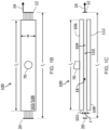
- FIGs. 1B and 1C are schematic plan and side views showing the principal optical components of the RF slab laser 100.
- the laser 100 includes a vacuum housing 114 (shown partially cut away in FIG. 1A ) that forms a vacuum enclosure to contain a gaseous lasing medium.
- the lasing medium of a slab laser is a plasma of a gas, most commonly carbon dioxide as the active molecule, although other gases such as carbon monoxide, helium and nitrogen as well as gas mixtures containing one or more of these gases are known.
- the laser 100 further comprises a top electrode 102 driven with RF power and a bottom electrode 108 which is grounded, the two electrodes having respective inwardly facing surfaces 104, 110 as well as outwardly facing surfaces 106, 108 that face outwards towards the walls of the vacuum housing 114.
- both electrodes 102, 108 are arranged inside the vacuum housing 114.
- the inwardly facing surfaces 104 and 110 of the top and bottom electrodes 102 and 108 are spaced apart by a gap of thickness 't', and each have a width 'w' and a length 'ls' to form a slab (see FIGs. 1B and 1C ).
- the gap is dimensioned to allow a plasma discharge 18, shown schematically with the stippling, to be formed by applying an RF electrical drive signal to the top electrode 102 while the bottom electrode is grounded.
- the top electrode 102 is therefore sometimes referred to as the live, hot or driven electrode and the bottom electrode 108 as the ground(ed) electrode.
- a resonator cavity for the laser is formed by a pair of mirrors 20, 22.
- Mirror 20 is an end reflector of ideally 100% reflectivity.
- Mirror 22 is an output coupler which may provide output coupling by being partially transmissive (as would be a usual choice for a stable resonator design), or, as schematically illustrated, with edge coupling by configuring the cavity such that a small portion of the beam path passes by the lateral edge of the output mirror (as would be a usual choice for an unstable confocal resonator design) so that the output beam, labelled 24, is emitted from the side of the output mirror 22.
- the cavity mirrors are placed outside the slab, so the cavity length is greater than the slab length. It will also be understood that the cavity mirrors may be planar or curved.
- a vacuum flange 70 for feed-through of the RF drive signal and the coolant fluid to the top electrode 102 extends into contact with the outwardly facing surface 106.
- the vacuum flange 70 is sealingly mounted in an access aperture 116 in the vacuum housing 114.
- the vacuum flange 70 has end portions of a plurality of hollow conductors 62 mounted therein.
- the top ends of the hollow conductors 62 are connected via electrically insulating pipe fitting connections 86, e.g. made of plastic, to respective coolant pipes 88 which serve to carry coolant fluid, e.g. water, into and out of the vacuum housing 114, where the water is circulated through or over the top electrode 102 via one or more fluid circulation channels 80. Coolant fluid is thereby passed through the vacuum flange 70 around the top electrode 102 and then back out of the vacuum flange 70.
- coolant fluid is thereby passed through the vacuum flange 70 around the top electrode 102 and then back out of the vacuum flange 70.
- two such fluid circulation channels 80a, 80b are schematically shown.
- Each fluid circulation channel 80 is formed by internal passages 82 within the top electrode 102.
- the internal passages 82 terminate in apertures 84 in the external (upper) surface 106 of the top electrode 102 and form fluid-flow connections with the proximal ends of the hollow conductors 62.
- the vacuum flange 70 is arranged with its underside or bottom surface abutting or affixed to the outwardly facing surface of the top electrode 102.
- the hollow conductors 62 that are fed through the vacuum flange 70 are arranged collectively so that they connect the top electrode 102 at or close to its geometric center (in plan view). This provides for symmetric dispersion of RF energy over the top electrode 102.
- the connections need not be positioned at the geometric center and could be anywhere along the outwardly facing surface of the top electrode 102.
- Variants for the ground electrode 108 would include having the ground electrode 108 formed integrally with the vacuum housing 114 or with its outwardly facing surface 112 outside the vacuum enclosure, i.e. on the air side, and its inwardly facing surface 110 inside the vacuum housing 114.
- Variants for the live electrode 102 would include having the its outwardly facing surface 106, or at least a portion thereof where the hollow conductors are connected, outside the vacuum enclosure and its inwardly facing surface 104 inside the vacuum housing 114.
- the hollow conductors 62 need not all be connected to the outwardly facing surface 106 of the live electrode 102 in a confined area as in the present embodiment.
- the hollow conductors 62 may have their connections to the live electrode distributed, e.g. evenly spaced apart, along the exposed, i.e. air side, part of the length of the outwardly facing surface 106 of the live electrode 102, e.g. singly or in pairs.
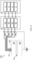
- FIG. 2 is a schematic block diagram showing the principal electrical components of the laser 100.
- An RF source 5 is provided which comprises a plurality of RF power amplifiers 6.
- the RF signals output from the RF power amplifiers 6 are supplied to associated impedance matching circuits 10 which together form an impedance matching network 8.
- the outputs of the impedance matching circuits 10 are fed into the vacuum enclosure through the vacuum flange 70.
- Each RF supply line is then connected separately and individually to the outwardly facing surface 106 of the top electrode 102.
- the impedance matching network 8 has its circuit elements distributed between the PCB module 25, the hollow conductors 62 and the vacuum flange 70.
- FIG. 3 shows the PCB module 25 in more detail.
- the PCB module 25 is built around a PCB 30.
- the PCB module 25 has RF power connectors 12 which are the inputs into the impedance matching circuits 10 via which the outputs from the RF power amplifiers 6 are received.
- the PCB 30 has an at least approximately centrally positioned aperture 34, i.e. a through-hole, which is dimensioned and positioned to allow the hollow conductors 62 to pass therethrough.
- the PCB module 25 accommodates components for four impedance matching circuits 10, these being arranged in four quadrants of the PCB 30 around the aperture 34.
- Each RF power connector 12 feeds the RF drive current received from its associated RF power amplifier 6 through an associated inductive strap (or ribbon or coil) 56 having a first end 52 and a second end 54, the inductive strap 56 forming a first inductor element.
- the first ends 52 are electrically connected to the upper surface of the PCB 30, for example on one of the conductive pads 32.
- the second ends 54 are located at or adjacent the PCB aperture 34 and are connected to respective ones of the hollow conductors 62 (not shown in FIG. 3 ).
- the PCB 30 is additionally used as a basis for forming one or more capacitors 45 for each of the impedance matching circuits 10.
- the PCB 30 forms a dielectric for the capacitors and the plates of each capacitor are formed respectively on the top and bottom sides of the PCB 30 by top conductive pads 32 and one or more bottom conductive pads 40.
- One of the conductive pads 32 of each impedance matching circuit 10 is connected to its RF power connector 12, thereby connecting each conductive pad 32 to its associated RF power amplifier 6.
- the bottom conductive pad 40 can be a single contiguous plate shared commonly by all the capacitors. Alternatively, a separate conductive pad 40 could be formed for each of the conductive pads 32 or for groups thereof.
- the inductive straps 56 are each configured to be easily removable so that different ones can be exchanged to trim the impedance matching when setting up the laser.
- the available inductive straps 56 may differ in shape, length and/or some other parameter which changes their inductance to allow an appropriate selection to be found.
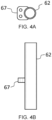
- FIGs. 4A and 4B are plan and side section views of a single one of the hollow conductors 62.
- the hollow conductor 62 may be conveniently formed by a section of copper pipe to which is soldered or otherwise affixed a connection tab 67, which allows a second end 54 of one of the inductive straps 56 to be fastened thereto.
- the fastening may be done with fastening bolts (not shown) which may be screwed into threaded holes in the lateral tabs 67.
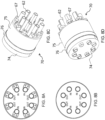
- FIGs. 5A-5D show a vacuum flange 70 in plan view from above and below as well as perspective view from above and below.
- the vacuum flange 70 comprises a base 74, which has the form of a circular disc and is a solid piece made of metal or a metallic material, a sleeve 75, which has the form of a hollow cylinder enclosing the hollow conductors 62, and an electrically insulating connector 76, which has the form of a band or ring and is made, for example, of a ceramic material.
- the vacuum flange 70 is four-way, i.e. has four hollow conductors 62 integrated into it.
- the vacuum flange sleeve 75 is made of metal in our examples manufactured to date, but could alternatively be made of a ceramic material or other electrically insulating material as well as a metallic material.
- the ring-shaped connector 76 forms a junction piece between the base 74 and sleeve 75, and is inserted in between them.
- the upper and lower end surfaces of the ring-shaped connector may be metallized to facilitate respective solder joints being formed with the base 74 and with the sleeve 75.
- the outer surface of the ring-shaped connector 76 forms a vacuum-tight connection with the access aperture 116 in the vacuum housing 114.
- the hollow conductors 62 which are arranged extending parallel to each other, extend out of the flange 70 and are located in a vacuum-tight manner within the flange base 74, i.e. a length portion of each hollow conductor 62 is embedded in the flange base 74, e.g. with a suitable solder connection.
- the bottom ends of the hollow conductors 62 i.e. the vacuum-side ends, may terminate flush with the the inside surface of the flange base 74, i.e. on its vacuum side, or extend out a certain distance from the inside surface of the flange base 74 (as shown in FIG. 5D ). It is noted that the lateral tabs 67 are located on the air-side of the vacuum flange 70.
- the hollow conductors 62 and the flange base 74 collectively provide a second inductor through their self-inductance.
- FIG. 6 shows a circuit diagram of a single one of the impedance matching circuits 10.
- a capacitor 45 of capacitance C1 is implemented by one or more conductive pads 32 and the common conductive pad 40 with the PCB 30 acting as the dielectric.
- a first inductor 50 of inductance Ll is provided by one of the inductive straps 56, the inductance of which is adjustable as necessary be swapping out different ones from the available set of inductive straps 56.
- a second inductor 60 of inductance L2 is provided by the hollow conductor 62 and its mounting in the vacuum flange 70. The second inductance L2 is fixed in the present design and depends on the outer diameter and the length of the hollow conductors 62.
- the impedance matching circuit 10 may additionally include one or more reactances or reactive impedance components (resistive, capacitive, inductive or a combination of these) (not shown), which may be arranged on the PCB 30.
- the reactances can be electrically connected to any of: the RF power connectors 12, the conductive pads 32, the inductive straps 56 and the hollow conductors 62 either in parallel or in series, as necessary for achieving desired impedance matching between the RF power amplifier 6 and the top electrode 102.
- FIG. 7 is a circuit diagram showing the impedance matching network 8 consisting of four of the impedance matching circuits 10 shown in FIG. 6 which deliver four RF supply lines through the vacuum flange 70 as described above.
- Capacitors C1a, C1b, C1c and C1d are the capacitors implemented by conductive pads 32 and 40.
- First inductors L1a, L1b, L1c and L1d are respective ones of the first inductors 50 formed by the inductive straps 56, whose inductance is changeable as needed.
- Second inductors L2a, L2b, L2c and L2d are respective ones of the second inductors 60 formed by respective ones of the hollow conductors 62.
- the capacitors C1a, C1b, C1c and C1d are electrically connected to four RF power amplifiers 6 in parallel.
- the first inductors L1a, L1b, L1c and L1d and the second inductors L2a, L2b, L2c and L2d are electrically connected to the four RF power amplifiers 6 in series.
- FIGs. 8A-8D correspond to FIGs. 5A-5D and show another example vacuum flange 70 which differs from that of FIGs. 5A-5D in that there are eight hollow conductors instead of four.
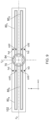
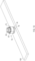
- FIGs. 9 and 10 show in plan and perspective view a top electrode 102 and vacuum flange 70, the vacuum feed-through being as shown in FIGs. 8A-8D .
- the top electrode 102 is provided with internal passages that form four fluid circulation channels 80a, 80b, 80c, 80d each with its own input and output apertures 84 on the external (top) surface of the electrode 102.
- a useful feature of this design with four fluid circulation channels is that the cooling is relatively even across the electrode both lengthways and crossways when viewed in plan view and also symmetric both lengthways (x-direction) and crossways (y-direction), i.e. symmetric about both a centrally positioned crossways plane Y0 and a centrally positioned lengthways plane X0 as illustrated.
- the flow paths can be arranged such that the outward flow paths are arranged laterally on the inside and the inward flow (return) paths are arranged laterally on the outside.
- the coolant fluid entering the electrode which is cold, is therefore piped through the more central part of the electrode 102 body (closer to the X0 plane), where the electrode would be the hottest absent any cooling, whereas the warmer coolant fluid returning from the electrode ends flows closer to the sides of the electrode (farther away from the X0 plane), thereby reducing the temperature gradient crossways across the electrode.
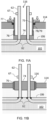
- FIGs. 11A, 11B and 11C are schematic section views showing three different implementation examples for arranging the hollow conductors to supply RF drive signal and coolant fluid to the top electrode.
- FIG. 11A shows an arrangement as described above and shown, for example in FIGs. 5A-5D .
- the vacuum housing 114 encloses a vacuum space which is indicated by stippling in the drawing.
- the top electrode 102 is arranged inside the vacuum space and by way of example two of the internal passages 82 are shown, these forming the channels for circulating coolant fluid around the top electrode 102.
- the passages 82 terminate in apertures in the outwardly facing surface of the top electrode.
- a ring-shaped connector 76 forms a butting, vacuum-tight connection with the vacuum flange base 74.
- a vacuum flange sleeve 75 is arranged in butting, vacuum-tight connection over the ring-shaped connector 76.
- An upper portion of the outer surface of the vacuum flange sleeve 75 forms a vacuum-tight connection with the inside rim surface of the vacuum housing aperture 116 via an O-ring 78 which sits in a annular groove 79 formed in the top surface of the vacuum housing 114 adjacent its aperture 116.
- the O-ring 78 is squashed down and laterally extended to form the vacuum-tight connection between vacuum housing 114 and sleeve 75 via a flange piece 77 that is screwed down on the top surface of the vacuum housing 114 as indicated schematically by the downward arrows.
- Length portions of the hollow conductors 62 are embedded in the vacuum flange base 74 in a vacuum-tight manner.
- the vacuum flange base 74 is made of electrically conducting material.
- the inwardly facing surface of vacuum flange base 74 is connected with the outwardly facing surface of the top electrode 102 in a fluid-tight and vacuum-tight manner.
- the proximal ends of the hollow conductors 62 align with the fluid input and output apertures of the passages 82 to provide a fluid-tight connection for the coolant fluid circulation paths.
- the bottom, inwardly facing surface of the vacuum flange base 74 abuts or is fixedly connected to the outwardly facing surface of the top electrode 102 in a fluid-tight and vacuum-tight manner, all that is needed for the coolant fluid circulation path to be formed is alignment of the passage apertures and the proximal ends of the hollow conductors and a fluid-tight connection where they meet.
- the proximal ends of the hollow conductors also need to be in good electrical contact with the top electrode in order for the RF drive signal to be transmitted.
- FIG. 11B shows an alternative implementation example which is described by comparison with the example of FIG. 11A .
- the vacuum flange base 74 does not extend to the top electrode 102. Rather, it is thinner and provides a vacuum seal through its radially outer face which is in vacuum-tight connection with the radially inner surface of the ring-shaped connector 76.
- the hollow conductors 62 have a length portion embedded in the base 74 in the same way as in the FIG. 11A design. Compared with the FIG. 11A design there is no counterpart of the sleeve part 75.
- the proximal ends of the hollow conductors 62 are connected to the passages' input and output apertures on the outwardly facing surface of the top electrode 102 in a fluid-tight and vacuum-tight manner. This may be effected with any suitable means; by way of example the drawing shows O-rings seated in counterbored recesses at the input and output apertures.
- FIG. 11C shows a further alternative implementation example which is described by comparison with the examples of FIGs. 11A and 11B .
- the electrically insulating connector 76 extends from the access aperture 116 of the vacuum housing 114 down into the vacuum space all the way to the outwardly facing surface of the top electrode 102 where it forms a vacuum-tight seal with the first electrode.
- the electrically insulating connector 76 is shaped and dimensioned in plan view to match the shape and dimensions of the access aperture 116, so in the illustrated example has the shape of a cylindrical tube to match the circular shape of the access aperture 116.
- a suitable ceramic material may be used for the connector 76.
- the vacuum-tight connection between the electrically insulating connector 76 and the top electrode 102 may be effected by any suitable means.
- the ceramic tube connector 76 could be vacuum-sealed to the top electrode by pushing it into an annular groove cut into the top of the electrode which accommodates a sealing O-ring (not shown).
- Another option would be to braze or otherwise affix an intermediate metal ring to the proximal end of the ceramic tube connector 76 to allow the intermediate metal ring to be brazed to the top electrode 102.
- An advantage of this implementation is that the hollow conductors do not enter the vacuum space, so their proximal end connections to the top electrode 102 are also outside the vacuum space, so only need to be fluid-tight, i.e. they do not need to be vacuum-tight.
- This may be effected with any suitable means; by way of example the drawing shows O-rings seated in counterbored recesses at the input and output apertures.
- a base 74 is included which has the hollow conductors embedded into it but which is not functionally part of the vacuum flange 70.
- the vacuum flange 70 in this embodiment consists solely of the electrically insulating connector 76.
- the base 74 in the illustrated example merely serves to mechanically and electrically connect the hollow conductors, which may be convenient but is not essential. In variants of this design, the illustrated base 74 may be omitted.
- the live electrode may be made according to the "inserts" and “expansions” design approach of the modified embodiment of the above-referenced US2010189156A1 , whereby the outwardly facing surface can be kept air side along substantially the entire length of the live electrode.
- the hollow conductors can then be connected distributed along substantially the entire length of the live electrode, e.g. singly or pairwise, as already mentioned further above.
- An embodiment can be envisaged with one fluid circulation channel supplied by two hollow conductors electrically connected to two impedance matching circuits supplied from two RF power amplifiers.
- a convenient arrangement is when one pair of hollow conductors is associated with one fluid circulation channel.
- the number of circulation channels that pass coolant around the top electrode can be freely chosen, i.e. is not restricted to 2 or 4 as in the illustrated examples, but may be any number from 1 to 5, 6, 7, 8 or more.
- alternative designs for the coolant passages in the top electrode may be envisaged in which a single hollow conductor has its fluid flow split into two (or more) as it enters the top electrode to supply two (or more) different coolant channels within the top electrode.
- the same arrangement as described in detail above for the top electrode may be replicated for the bottom electrode.
- This may be of interest in particular for designs in which both the top and bottom electrodes are driven with RF, i.e. when an RF source is connected to the outwardly facing surfaces of both the top and bottom electrodes, the bottom electrode thereby being supplied with an additional RF electrical drive signal that is out of phase with the RF electrical drive signal supplied to the top electrode.
Landscapes
- Physics & Mathematics (AREA)
- Electromagnetism (AREA)
- Engineering & Computer Science (AREA)
- Plasma & Fusion (AREA)
- Optics & Photonics (AREA)
- Lasers (AREA)
Abstract
Description
- The present disclosure relates to a radio frequency (RF) slab laser.
- An RF slab laser is a laser with a kind of flat planar construction, which in its simplest form has only two electrodes. The two electrodes are arranged on top of each other so that their inwardly facing surfaces form a gap of a certain thickness. When an RF drive signal is applied to the electrodes, a plasma discharge of a gas, such as carbon dioxide, is formed in the gap. The plasma provides a gain medium capable of supporting stimulated emission within a resonator cavity formed by end mirrors which are typically arranged just outside the gap. The electrodes, or at least the gap between them where the plasma is to be formed, needs to be in a vacuum. In most commercial designs, the plasma is induced between a "cold" ground electrode and an RF driven "live" or "hot" electrode. However, it is also possible to use two RF electrodes that are both "live" and driven with complementary phases.
- In RF slab lasers there is inevitably a heat management issue with the electrodes, in particular for the live electrode. For RF slab lasers with lower output powers, an internal conduction cooling path to an external air-cooled heat exchanger is generally adequate, whereas for higher laser output powers the electrodes typically need to be cooled by circulating a coolant fluid, typically water, around the electrode.
- Some known approaches for water cooling of high powered RF slab lasers are now summarized.
-
US5123028 discloses a carbon dioxide slab laser with water cooling for the live electrode and the ground electrode. For each electrode, a coolant loop is provided by a copper pipe which is soldered into channels that have been machined out of the outwardly facing surfaces of the electrodes. The ends of the pipes pass through the end plate of the vacuum housing and are electrically grounded. The center segment of the coolant pipe that is in physical contact with the live electrode needs to be electrically isolated from the grounded part of the coolant pipe. This is done with a pair of in-line union connectors made of an electrically insulating material, so that the part of the pipe which is live is electrically isolated from the remainder of the pipe which is grounded. A drawback of the design ofUS5123028 is the need for the insulating union connectors. These add cost to the laser manufacture and are a potential water leak source as well as sometimes being an unwanted generator of RF discharge, since they form a junction between live and ground. -
US8731015B2 discloses a carbon dioxide slab laser which has a special design for cooling the live electrode involving a double-folded assembly of coolant tubes that are in thermal contact with the live electrode. The coolant tubes have a very high RF-impedance which avoids the need for them to be electrically insulated from the laser housing and so dispenses with the need for the insulating union connectors ofUS5123028 . The coolant tube is dimensioned to extend beyond the end of the electrode through which it passes by an amount that provides a sufficiently high inductance at the RF frequency (e.g. about 100 MHz) that it can contact the grounded vacuum housing without causing a short circuit. -
US2010189156A1 discloses a carbon dioxide slab laser in which both the live and ground electrodes have their outwardly facing surfaces outside the vacuum enclosure. Coolant channels are formed in each electrode by four lengthways grooves formed in the outwardly facing surface. On each electrode an insert piece is screwed onto the outwardly facing surface to close the grooves in a liquid-tight manner and thereby form the coolant channels. For each electrode, the coolant fluid is introduced into the ends of the groove channels by a pair of connector pipes. The coolant fluid then flows along the electrode from one end to the other through the groove channels. The coolant fluid is then extracted from the other end by another pair of connector pipes. -
US9263849B2 - According to one aspect of the disclosure, there is provided an RF slab laser comprising:
- a first electrode and a second electrode having respective inwardly and outwardly facing surfaces, wherein their respective inwardly facing surfaces face each other and are spaced apart by a gap forming a slab waveguide of a thickness dimensioned to allow a plasma discharge to be formed by driving at least the first electrode with an RF drive signal, the first electrode being provided with at least one fluid circulation channel for distributing coolant fluid around the first electrode;
- a vacuum housing enclosing at least the inwardly facing surfaces of the first and second electrodes inside a vacuum space; and
- a plurality of hollow conductors connected to the outwardly facing surface of the first electrode to supply the RF drive signal to the first electrode and the coolant fluid to the at least one fluid circulation channel of the first electrode.
- In some embodiments, the outwardly facing surface of the first electrode is inside the vacuum space. The vacuum housing is then provided with an access aperture and a vacuum flange is arranged in the access aperture to form a vacuum-tight seal with the vacuum housing with the hollow conductors each having an intermediate length portion embedded in the vacuum flange. The vacuum flange thus serves as a feed-through for the hollow conductors to supply the RF drive signal and the coolant fluid to the first electrode
- In other embodiments, at least a portion of the outwardly facing surface of the first electrode is outside the vacuum space and is used to connect the hollow conductors. The hollow conductors thus remain outside the vacuum space obviating the need for a vacuum feed-through. This may be implemented by the vacuum housing being provided with an access aperture and by providing an electrically insulating connector that extends from the access aperture, where it forms a vacuum-tight seal, to the outwardly facing surface of the first electrode, where it forms a further vacuum-tight seal. Said portion of the outwardly facing surface of the first electrode that is outside the vacuum space is thus formed by the access aperture in combination with the electrically insulating connector which may be hollow, e.g. a cylindrical tube that is dimensioned to match a circular-shaped access aperture.
- There are different alternatives for forming the fluid circulation channels. In some embodiments, each fluid circulation channel comprises at least one internal passage formed within the first electrode which terminates in apertures in a surface of the first electrode, for example the outwardly facing surface of the first electrode, for coolant fluid input and output, the fluid input and output apertures being arranged in fluid-flow connection with proximal ends of the hollow conductors. One implementation of such embodiments is for the fluid input and output apertures to be arranged aligned with the proximal ends of the hollow conductors. In other embodiments, the fluid circulation channel(s) comprise further hollow conductors arranged in thermal contact with the outwardly facing surface of the first electrode (e.g. by soldering as described for the live electrode in the above-referenced
US5123028 ) and in fluid-flow connection with the hollow conductors of the vacuum feed-through. The hollow conductors may be formed integrally with the further hollow conductors, i.e. as single hollow conductors, similar to what is shown for the live electrode in the above-referencedUS5123028 . In such embodiments, the coolant channels are thus formed by hollow conductors rather than internal coolant channels formed within the electrode(s). - In some embodiments, the first electrode has an elongate shape with a length several times times greater than its width (e.g. at least 5 or 10 times) and the hollow conductor connections are positioned at least approximately mid-way along the outwardly facing surface of the first electrode, thereby subdividing the first electrode into first and second arms. Each arm is preferably provided with at least one fluid circulation channel, namely a first fluid circulation channel extending around the first arm of the first electrode and a second fluid circulation channel extending around the second arm of the first electrode.
- In one particular implementation, the first fluid circulation channel is connected to be supplied with coolant fluid by first and second ones of the hollow conductors and the second fluid circulation channel may be connected to be supplied with coolant fluid by third and fourth ones of the hollow conductors. This is a 4-pin arrangement of hollow conductors which allows the first electrode to be supplied directly with four independent RF supplies, i.e. the RF drive signal has four independent components which are not combined but rather are connected independently to the first electrode by four of the hollow conductors. Here there may be first and second fluid circulation channels extending around the first arm of the first electrode and third and fourth fluid circulation channels extending around the second arm of the first electrode.
- In another particular implementation, the first fluid circulation channel is connected to be supplied with coolant fluid by first and second ones of the hollow conductors and wherein the second fluid circulation channel is connected to be supplied with coolant fluid by third and fourth ones of the hollow conductors, wherein the third fluid circulation channel is connected to be supplied with coolant fluid by fifth and sixth ones of the hollow conductors and wherein the fourth fluid circulation channel is connected to be supplied with coolant fluid by seventh and eighth ones of the hollow conductors. This is an 8-pin arrangement of hollow conductors which allows the first electrode to be supplied directly with eight independent RF supplies, i.e. the RF drive signal has eight independent components which are not combined but rather are connected independently to the first electrode by eight of the hollow conductors. Here the first and second fluid circulation channels may be jointly arranged to cool either side of the first arm, wherein the third and fourth fluid circulation channels may be jointly arranged to cool either side of the second arm, thereby to avoid a temperature gradient forming crossways between opposite sides of the first electrode.
- A convenient construction feature is for each hollow conductor to be provided with a tab located outside the vacuum housing via which it is supplied with the RF drive signal, e.g. by fixing one end of an inductive strap to the tab.
- The laser may further comprise a plurality of RF amplifiers and associated impedance matching circuits for generating a plurality of components of the RF drive signal, respective ones of the hollow conductors being connected to receive respective ones of the RF drive signal components output from respective ones of the impedance matching circuits. The RF amplifiers, impedance matching circuits, and hollow conductors may be connected to form one or more groups. Each group may consist of two RF amplifiers, two impedance matching circuits and two hollow conductors. Moreover, each said group can be associated with one circulation channel. Here one hollow conductor of a group supplies coolant fluid and the other extracts it. The laser may further comprise electrically insulating connector pieces connected to distal ends of the hollow conductors, the connector pieces being configured to connect with respective fluid supply lines.
- In further embodiments, the above-mentioned design features of the first electrode may be replicated for the second electrode. This may be of interest in particular for designs in which both the first and second electrodes are driven with RF, e.g. when the first and second electrodes are driven with respective RF drive signals that are out of phase with each other.
- In the following, the present invention will further be described by way of example only with reference to exemplary embodiments illustrated in the figures.
-
FIG. 1A is an exploded perspective view showing an RF slab laser according to an embodiment of the invention with an RF supply consisting of four RF amplifiers, an impedance matching network consisting of four impedance matching circuits, a four-way vacuum feed-through and a top electrode with two fluid circulation channels for cooling. -
FIGs. 1B and 1C are schematic plan and side views showing principal optical components of the RF slab laser ofFIG. 1A . -
FIG. 2 is a block diagram showing principal electrical components of the laser. -
FIG. 3 is a perspective view showing further details of the construction ofFIG. 1A . -
FIGs. 4A and 4B are plan and side section views of a hollow conductor. -
FIGs. 5A to 5D show a 4-way vacuum feed-through in plan view from above and below as well as perspective view from above and below. -
FIG. 6 is a circuit diagram of an impedance matching circuit. -
FIG. 7 is a circuit diagram of an impedance matching network consisting of four impedance matching circuits as shown inFIG. 6 . -
FIGs. 8A to 8D show an 8-way vacuum feed-through in plan view from above and below as well as perspective view from above and below. -
FIGs. 9 and10 are schematic plan and perspective views of a top electrode and vacuum feed-through for a further embodiment in which the top electrode has four fluid circulation channels and is connected to an 8-way vacuum feed-through. -
FIGs. 11A, 11B and11C show three different implementation examples for arranging the hollow conductors to supply RF drive signal and coolant fluid to the top electrode. - In the following detailed description, for purposes of explanation and not limitation, specific details are set forth in order to provide a better understanding of the present disclosure. It will be apparent to one skilled in the art that the present disclosure may be practiced in other embodiments that depart from these specific details.
-
FIG. 1A is an exploded perspective view showing anRF slab laser 100 according to an embodiment of the invention.FIGs. 1B and 1C are schematic plan and side views showing the principal optical components of theRF slab laser 100. Thelaser 100 includes a vacuum housing 114 (shown partially cut away inFIG. 1A ) that forms a vacuum enclosure to contain a gaseous lasing medium. The lasing medium of a slab laser is a plasma of a gas, most commonly carbon dioxide as the active molecule, although other gases such as carbon monoxide, helium and nitrogen as well as gas mixtures containing one or more of these gases are known. Thelaser 100 further comprises atop electrode 102 driven with RF power and abottom electrode 108 which is grounded, the two electrodes having respective inwardly facingsurfaces surfaces vacuum housing 114. In the illustrated design, bothelectrodes vacuum housing 114. - The inwardly facing
surfaces bottom electrodes FIGs. 1B and 1C ). The gap is dimensioned to allow aplasma discharge 18, shown schematically with the stippling, to be formed by applying an RF electrical drive signal to thetop electrode 102 while the bottom electrode is grounded. In the following, thetop electrode 102 is therefore sometimes referred to as the live, hot or driven electrode and thebottom electrode 108 as the ground(ed) electrode. A resonator cavity for the laser is formed by a pair ofmirrors Mirror 20 is an end reflector of ideally 100% reflectivity.Mirror 22 is an output coupler which may provide output coupling by being partially transmissive (as would be a usual choice for a stable resonator design), or, as schematically illustrated, with edge coupling by configuring the cavity such that a small portion of the beam path passes by the lateral edge of the output mirror (as would be a usual choice for an unstable confocal resonator design) so that the output beam, labelled 24, is emitted from the side of theoutput mirror 22. Because of construction considerations, the cavity mirrors are placed outside the slab, so the cavity length is greater than the slab length. It will also be understood that the cavity mirrors may be planar or curved. Avacuum flange 70 for feed-through of the RF drive signal and the coolant fluid to thetop electrode 102 extends into contact with the outwardly facingsurface 106. - The
vacuum flange 70 is sealingly mounted in anaccess aperture 116 in thevacuum housing 114. Thevacuum flange 70 has end portions of a plurality ofhollow conductors 62 mounted therein. The top ends of thehollow conductors 62 are connected via electrically insulating pipe fitting connections 86, e.g. made of plastic, torespective coolant pipes 88 which serve to carry coolant fluid, e.g. water, into and out of thevacuum housing 114, where the water is circulated through or over thetop electrode 102 via one or morefluid circulation channels 80. Coolant fluid is thereby passed through thevacuum flange 70 around thetop electrode 102 and then back out of thevacuum flange 70. InFIG. 1A , two such fluid circulation channels 80a, 80b are schematically shown. Eachfluid circulation channel 80 is formed byinternal passages 82 within thetop electrode 102. In the illustrated embodiment, there is one hollow conductor for input and one for output for each fluid circulation channel 80a, 80b. Theinternal passages 82 terminate inapertures 84 in the external (upper)surface 106 of thetop electrode 102 and form fluid-flow connections with the proximal ends of thehollow conductors 62. Thevacuum flange 70 is arranged with its underside or bottom surface abutting or affixed to the outwardly facing surface of thetop electrode 102. Thehollow conductors 62 that are fed through thevacuum flange 70 are arranged collectively so that they connect thetop electrode 102 at or close to its geometric center (in plan view). This provides for symmetric dispersion of RF energy over thetop electrode 102. Alternatively, in other designs, the connections need not be positioned at the geometric center and could be anywhere along the outwardly facing surface of thetop electrode 102. - Variants for the
ground electrode 108 would include having theground electrode 108 formed integrally with thevacuum housing 114 or with its outwardly facingsurface 112 outside the vacuum enclosure, i.e. on the air side, and its inwardly facingsurface 110 inside thevacuum housing 114. Variants for thelive electrode 102 would include having the its outwardly facingsurface 106, or at least a portion thereof where the hollow conductors are connected, outside the vacuum enclosure and its inwardly facingsurface 104 inside thevacuum housing 114. Thehollow conductors 62 need not all be connected to the outwardly facingsurface 106 of thelive electrode 102 in a confined area as in the present embodiment. Rather, in a variant in which at least a substantial proportion of the length of the outwardly facingsurface 106 of thelive electrode 102 is outside the vacuum, e.g. more than half or at least three quarters, thehollow conductors 62 may have their connections to the live electrode distributed, e.g. evenly spaced apart, along the exposed, i.e. air side, part of the length of the outwardly facingsurface 106 of thelive electrode 102, e.g. singly or in pairs. -
FIG. 2 is a schematic block diagram showing the principal electrical components of thelaser 100. An RF source 5 is provided which comprises a plurality ofRF power amplifiers 6. The RF signals output from theRF power amplifiers 6 are supplied to associatedimpedance matching circuits 10 which together form animpedance matching network 8. The outputs of theimpedance matching circuits 10 are fed into the vacuum enclosure through thevacuum flange 70. Each RF supply line is then connected separately and individually to the outwardly facingsurface 106 of thetop electrode 102. Theimpedance matching network 8 has its circuit elements distributed between thePCB module 25, thehollow conductors 62 and thevacuum flange 70. -
FIG. 3 shows thePCB module 25 in more detail. Structurally, thePCB module 25 is built around aPCB 30. ThePCB module 25 hasRF power connectors 12 which are the inputs into theimpedance matching circuits 10 via which the outputs from theRF power amplifiers 6 are received. ThePCB 30 has an at least approximately centrally positioned aperture 34, i.e. a through-hole, which is dimensioned and positioned to allow thehollow conductors 62 to pass therethrough. ThePCB module 25 accommodates components for fourimpedance matching circuits 10, these being arranged in four quadrants of thePCB 30 around the aperture 34. EachRF power connector 12 feeds the RF drive current received from its associatedRF power amplifier 6 through an associated inductive strap (or ribbon or coil) 56 having afirst end 52 and asecond end 54, theinductive strap 56 forming a first inductor element. The first ends 52 are electrically connected to the upper surface of thePCB 30, for example on one of theconductive pads 32. The second ends 54 are located at or adjacent the PCB aperture 34 and are connected to respective ones of the hollow conductors 62 (not shown inFIG. 3 ). ThePCB 30 is additionally used as a basis for forming one ormore capacitors 45 for each of theimpedance matching circuits 10. Namely, thePCB 30 forms a dielectric for the capacitors and the plates of each capacitor are formed respectively on the top and bottom sides of thePCB 30 by topconductive pads 32 and one or more bottomconductive pads 40. One of theconductive pads 32 of eachimpedance matching circuit 10 is connected to itsRF power connector 12, thereby connecting eachconductive pad 32 to its associatedRF power amplifier 6. The bottomconductive pad 40 can be a single contiguous plate shared commonly by all the capacitors. Alternatively, a separateconductive pad 40 could be formed for each of theconductive pads 32 or for groups thereof. Theinductive straps 56 are each configured to be easily removable so that different ones can be exchanged to trim the impedance matching when setting up the laser. The availableinductive straps 56 may differ in shape, length and/or some other parameter which changes their inductance to allow an appropriate selection to be found. -
FIGs. 4A and 4B are plan and side section views of a single one of thehollow conductors 62. Thehollow conductor 62 may be conveniently formed by a section of copper pipe to which is soldered or otherwise affixed aconnection tab 67, which allows asecond end 54 of one of theinductive straps 56 to be fastened thereto. The fastening may be done with fastening bolts (not shown) which may be screwed into threaded holes in thelateral tabs 67. -
FIGs. 5A-5D show avacuum flange 70 in plan view from above and below as well as perspective view from above and below. Thevacuum flange 70 comprises abase 74, which has the form of a circular disc and is a solid piece made of metal or a metallic material, asleeve 75, which has the form of a hollow cylinder enclosing thehollow conductors 62, and an electrically insulatingconnector 76, which has the form of a band or ring and is made, for example, of a ceramic material. Thevacuum flange 70 is four-way, i.e. has fourhollow conductors 62 integrated into it. Thevacuum flange sleeve 75 is made of metal in our examples manufactured to date, but could alternatively be made of a ceramic material or other electrically insulating material as well as a metallic material. The ring-shapedconnector 76 forms a junction piece between the base 74 andsleeve 75, and is inserted in between them. The upper and lower end surfaces of the ring-shaped connector may be metallized to facilitate respective solder joints being formed with thebase 74 and with thesleeve 75. The outer surface of the ring-shapedconnector 76 forms a vacuum-tight connection with theaccess aperture 116 in thevacuum housing 114. Thehollow conductors 62, which are arranged extending parallel to each other, extend out of theflange 70 and are located in a vacuum-tight manner within theflange base 74, i.e. a length portion of eachhollow conductor 62 is embedded in theflange base 74, e.g. with a suitable solder connection. The bottom ends of thehollow conductors 62, i.e. the vacuum-side ends, may terminate flush with the the inside surface of theflange base 74, i.e. on its vacuum side, or extend out a certain distance from the inside surface of the flange base 74 (as shown inFIG. 5D ). It is noted that thelateral tabs 67 are located on the air-side of thevacuum flange 70. Thehollow conductors 62 and theflange base 74 collectively provide a second inductor through their self-inductance. -
FIG. 6 shows a circuit diagram of a single one of theimpedance matching circuits 10. Acapacitor 45 of capacitance C1 is implemented by one or moreconductive pads 32 and the commonconductive pad 40 with thePCB 30 acting as the dielectric. Afirst inductor 50 of inductance Ll is provided by one of theinductive straps 56, the inductance of which is adjustable as necessary be swapping out different ones from the available set ofinductive straps 56. Asecond inductor 60 of inductance L2 is provided by thehollow conductor 62 and its mounting in thevacuum flange 70. The second inductance L2 is fixed in the present design and depends on the outer diameter and the length of thehollow conductors 62. It is therefore possible to design in a desired fixed value for L2 by adjusting these dimensions. Increasing the outer diameter of thehollow conductors 62 reduces the inductance L2 and increasing the length of thehollow conductors 62 increases the inductance L2. The first andsecond inductors RF power amplifier 6 in series and thecapacitor 45 is electrically connected to theRF power amplifier 6 in parallel with theinductors impedance matching circuit 10 may additionally include one or more reactances or reactive impedance components (resistive, capacitive, inductive or a combination of these) (not shown), which may be arranged on thePCB 30. The reactances can be electrically connected to any of: theRF power connectors 12, theconductive pads 32, theinductive straps 56 and thehollow conductors 62 either in parallel or in series, as necessary for achieving desired impedance matching between theRF power amplifier 6 and thetop electrode 102. -
FIG. 7 is a circuit diagram showing theimpedance matching network 8 consisting of four of theimpedance matching circuits 10 shown inFIG. 6 which deliver four RF supply lines through thevacuum flange 70 as described above. Capacitors C1a, C1b, C1c and C1d are the capacitors implemented byconductive pads first inductors 50 formed by theinductive straps 56, whose inductance is changeable as needed. Second inductors L2a, L2b, L2c and L2d are respective ones of thesecond inductors 60 formed by respective ones of thehollow conductors 62. The capacitors C1a, C1b, C1c and C1d are electrically connected to fourRF power amplifiers 6 in parallel. The first inductors L1a, L1b, L1c and L1d and the second inductors L2a, L2b, L2c and L2d are electrically connected to the fourRF power amplifiers 6 in series. As described inUS9263849B2 RF power amplifiers 6 and associatedimpedance matching circuits 10, which are each connected individually and separately to adjacent locations on thetop electrode 102, serves to deliver multiple RF power supply lines at multiple locations on thetop electrode 102. This can significantly reduce RF power loss compared with a standard design where multiple RF power supplies have their outputs combined outside the vacuum enclosure and fed through a single impedance matching circuit before being delivered to the top electrode through a single supply line. The heat generated by the impedance matching circuit is proportional to the square of the current. As a consequence a design having 'n' independent RF supply lines with associated impedance matching circuits that supply to 'n' locations on the top electrode means that each supply line carries one n-th of the total current injected into the live electrode, instead of a single RF supply line output from a single impedance matching circuit. This reduces the amount of heat generated by a factor 'n', e.g. a factor of four in the example of having four pairs of RF power amplifier and impedance matching circuit. -
FIGs. 8A-8D correspond toFIGs. 5A-5D and show anotherexample vacuum flange 70 which differs from that ofFIGs. 5A-5D in that there are eight hollow conductors instead of four. -
FIGs. 9 and10 show in plan and perspective view atop electrode 102 andvacuum flange 70, the vacuum feed-through being as shown inFIGs. 8A-8D . Thetop electrode 102 is provided with internal passages that form fourfluid circulation channels 80a, 80b, 80c, 80d each with its own input andoutput apertures 84 on the external (top) surface of theelectrode 102. A useful feature of this design with four fluid circulation channels is that the cooling is relatively even across the electrode both lengthways and crossways when viewed in plan view and also symmetric both lengthways (x-direction) and crossways (y-direction), i.e. symmetric about both a centrally positioned crossways plane Y0 and a centrally positioned lengthways plane X0 as illustrated. For example, to provide a more uniform temperature difference between the fluid circulation channels, the flow paths can be arranged such that the outward flow paths are arranged laterally on the inside and the inward flow (return) paths are arranged laterally on the outside. The coolant fluid entering the electrode, which is cold, is therefore piped through the more central part of theelectrode 102 body (closer to the X0 plane), where the electrode would be the hottest absent any cooling, whereas the warmer coolant fluid returning from the electrode ends flows closer to the sides of the electrode (farther away from the X0 plane), thereby reducing the temperature gradient crossways across the electrode. Although there may be some temperature gradient lengthways along the electrode as the distance increases from the central location of the vacuum flange 70 (i.e. distance from Y0 plane) as a consequence of the coolant fluid warming up, any such lengthwise temperature gradient will be gradual. -
FIGs. 11A, 11B and11C are schematic section views showing three different implementation examples for arranging the hollow conductors to supply RF drive signal and coolant fluid to the top electrode. -
FIG. 11A shows an arrangement as described above and shown, for example inFIGs. 5A-5D . Thevacuum housing 114 encloses a vacuum space which is indicated by stippling in the drawing. Thetop electrode 102 is arranged inside the vacuum space and by way of example two of theinternal passages 82 are shown, these forming the channels for circulating coolant fluid around thetop electrode 102. Thepassages 82 terminate in apertures in the outwardly facing surface of the top electrode. A ring-shapedconnector 76 forms a butting, vacuum-tight connection with thevacuum flange base 74. Avacuum flange sleeve 75 is arranged in butting, vacuum-tight connection over the ring-shapedconnector 76. An upper portion of the outer surface of thevacuum flange sleeve 75 forms a vacuum-tight connection with the inside rim surface of thevacuum housing aperture 116 via an O-ring 78 which sits in aannular groove 79 formed in the top surface of thevacuum housing 114 adjacent itsaperture 116. The O-ring 78 is squashed down and laterally extended to form the vacuum-tight connection betweenvacuum housing 114 andsleeve 75 via aflange piece 77 that is screwed down on the top surface of thevacuum housing 114 as indicated schematically by the downward arrows. Length portions of thehollow conductors 62 are embedded in thevacuum flange base 74 in a vacuum-tight manner. Thevacuum flange base 74 is made of electrically conducting material. The inwardly facing surface ofvacuum flange base 74 is connected with the outwardly facing surface of thetop electrode 102 in a fluid-tight and vacuum-tight manner. The proximal ends of thehollow conductors 62 align with the fluid input and output apertures of thepassages 82 to provide a fluid-tight connection for the coolant fluid circulation paths. With this implementation, since the bottom, inwardly facing surface of thevacuum flange base 74 abuts or is fixedly connected to the outwardly facing surface of thetop electrode 102 in a fluid-tight and vacuum-tight manner, all that is needed for the coolant fluid circulation path to be formed is alignment of the passage apertures and the proximal ends of the hollow conductors and a fluid-tight connection where they meet. The proximal ends of the hollow conductors also need to be in good electrical contact with the top electrode in order for the RF drive signal to be transmitted. -
FIG. 11B shows an alternative implementation example which is described by comparison with the example ofFIG. 11A . Unlike in the example ofFIG. 11A , in the example ofFIG. 11B , thevacuum flange base 74 does not extend to thetop electrode 102. Rather, it is thinner and provides a vacuum seal through its radially outer face which is in vacuum-tight connection with the radially inner surface of the ring-shapedconnector 76. Thehollow conductors 62 have a length portion embedded in the base 74 in the same way as in theFIG. 11A design. Compared with theFIG. 11A design there is no counterpart of thesleeve part 75. The proximal ends of thehollow conductors 62 are connected to the passages' input and output apertures on the outwardly facing surface of thetop electrode 102 in a fluid-tight and vacuum-tight manner. This may be effected with any suitable means; by way of example the drawing shows O-rings seated in counterbored recesses at the input and output apertures. -
FIG. 11C shows a further alternative implementation example which is described by comparison with the examples ofFIGs. 11A and 11B . In this example, the electrically insulatingconnector 76 extends from theaccess aperture 116 of thevacuum housing 114 down into the vacuum space all the way to the outwardly facing surface of thetop electrode 102 where it forms a vacuum-tight seal with the first electrode. The electrically insulatingconnector 76 is shaped and dimensioned in plan view to match the shape and dimensions of theaccess aperture 116, so in the illustrated example has the shape of a cylindrical tube to match the circular shape of theaccess aperture 116. A suitable ceramic material may be used for theconnector 76. The vacuum-tight connection between the electrically insulatingconnector 76 and thetop electrode 102 may be effected by any suitable means. For example, at its proximal end theceramic tube connector 76 could be vacuum-sealed to the top electrode by pushing it into an annular groove cut into the top of the electrode which accommodates a sealing O-ring (not shown). Another option would be to braze or otherwise affix an intermediate metal ring to the proximal end of theceramic tube connector 76 to allow the intermediate metal ring to be brazed to thetop electrode 102. An advantage of this implementation is that the hollow conductors do not enter the vacuum space, so their proximal end connections to thetop electrode 102 are also outside the vacuum space, so only need to be fluid-tight, i.e. they do not need to be vacuum-tight. This may be effected with any suitable means; by way of example the drawing shows O-rings seated in counterbored recesses at the input and output apertures. It is further noted that in the illustration abase 74 is included which has the hollow conductors embedded into it but which is not functionally part of thevacuum flange 70. Thevacuum flange 70 in this embodiment consists solely of the electrically insulatingconnector 76. The base 74 in the illustrated example merely serves to mechanically and electrically connect the hollow conductors, which may be convenient but is not essential. In variants of this design, the illustratedbase 74 may be omitted. - In addition to the implementation of
FIG. 11C , there are also other ways to construct the laser so that the outwardly facing surface of the first electrode is in part or indeed entirely or substantially entirely outside the vacuum space. For example the live electrode may be made according to the "inserts" and "expansions" design approach of the modified embodiment of the above-referencedUS2010189156A1 , whereby the outwardly facing surface can be kept air side along substantially the entire length of the live electrode. The hollow conductors can then be connected distributed along substantially the entire length of the live electrode, e.g. singly or pairwise, as already mentioned further above. - Various modifications from the specific embodiments described above may be envisaged.
- An embodiment can be envisaged with one fluid circulation channel supplied by two hollow conductors electrically connected to two impedance matching circuits supplied from two RF power amplifiers. Generally a convenient arrangement is when one pair of hollow conductors is associated with one fluid circulation channel. Moreover, the number of circulation channels that pass coolant around the top electrode can be freely chosen, i.e. is not restricted to 2 or 4 as in the illustrated examples, but may be any number from 1 to 5, 6, 7, 8 or more. Furthermore, alternative designs for the coolant passages in the top electrode may be envisaged in which a single hollow conductor has its fluid flow split into two (or more) as it enters the top electrode to supply two (or more) different coolant channels within the top electrode. These two (or more) coolant channels could remain separate downstream and have their fluid extracted by two (or more) hollow conductors. Alternatively, these two (or more) coolant channels could come back together downstream where they terminate at an aperture in the outwardly facing surface of the top electrode and have their coolant fluid extracted by a single hollow conductor. In other words, designs can be envisaged which do not have a two-to-one ratio of the number of hollow conductors to fluid circulation channel(s).
- Moreover, it will be understood that the same arrangement as described in detail above for the top electrode may be replicated for the bottom electrode. This may be of interest in particular for designs in which both the top and bottom electrodes are driven with RF, i.e. when an RF source is connected to the outwardly facing surfaces of both the top and bottom electrodes, the bottom electrode thereby being supplied with an additional RF electrical drive signal that is out of phase with the RF electrical drive signal supplied to the top electrode.
- It will be clear to one skilled in the art that many improvements and modifications can be made to the foregoing exemplary embodiments without departing from the scope of the present disclosure.
-
- 5
- RF supply
- 6
- RF power amplifier
- 8
- impedance matching network
- 10
- impedance matching circuit
- 12
- RF power connector
- 18
- plasma discharge
- 20
- rear mirror
- 22
- front mirror (output coupler)
- 24
- output beam
- 25
- PCB module
- 30
- printed circuit board (PCB)
- 32
- top conductive pads
- 34
- aperture
- 40
- bottom conductive pad(s)
- 45
- capacitor
- 50
- first inductor
- 52
- first end of 56
- 54
- second end of 56
- 56
- inductive strap (or ribbon or coil)
- 60
- second inductor
- 62
- hollow conductor
- 67
- connection tab of hollow conductor 66
- 70
- vacuum flange
- 74
- vacuum flange base (e.g. circular disc)
- 75
- vacuum flange sleeve (e.g. hollow cylinder)
- 76
- electrically insulating connector (e.g. ceramic ring)
- 77
- clamping flange
- 78
- O-ring
- 79
- groove in outer surface of vacuum housing
- 80
- fluid circulation channel (80a, 80b; 80a, 80b, 80c, 80d)
- 82
- internal passages in cooled electrode
- 84
- apertures in outwardly facing surface of cooled electrode
- 86
- pipe fitting union connections (plastic)
- 88
- coolant pipes
- C1
- capacitor
- L1
- first inductor
- L2
- second inductor
- 100
- RF slab laser
- 102
- top electrode
- 104
- top electrode inwardly facing surface
- 106
- top electrode outwardly facing surface
- 108
- bottom electrode
- 110
- bottom electrode inwardly facing surface
- 112
- bottom electrode outwardly facing surface
- 114
- vacuum housing
- 116
- access aperture
- Further aspects of the invention are defined in the following numbered clauses:
- 1. A radio frequency, RF, slab laser comprising:
- a first electrode and a second electrode having respective inwardly and outwardly facing surfaces, wherein their respective inwardly facing surfaces face each other and are spaced apart by a gap forming a slab waveguide of a thickness dimensioned to allow a plasma discharge to be formed by driving at least the first electrode with an RF drive signal, the first electrode being provided with at least one fluid circulation channel for distributing coolant fluid around the first electrode;
- a vacuum housing enclosing at least the inwardly facing surfaces of the first and second electrodes inside a vacuum space; and
- a plurality of hollow conductors connected to the outwardly facing surface of the first electrode to supply the RF drive signal to the first electrode and the coolant fluid to the at least one fluid circulation channel of the first electrode.
- 2. The laser of
clause 1, wherein the outwardly facing surface of the first electrode is inside the vacuum space, wherein the vacuum housing is provided with an access aperture, and wherein a vacuum flange is arranged in the access aperture to form a vacuum-tight seal with the vacuum housing, the vacuum flange having an intermediate length portion of each hollow conductor embedded therein. - 3. The laser of
clause 1, wherein at least a portion of the outwardly facing surface of the first electrode is outside the vacuum space, and wherein the hollow conductors connect to said portion. - 4a. The laser of clause 3, wherein the vacuum housing is provided with an access aperture, and wherein an electrically insulating connector extends from the access aperture, where it forms a vacuum-tight seal, to the outwardly facing surface of the first electrode, where it forms a further vacuum-tight seal, and defines said portion of the outwardly facing surface of the first electrode that is outside the vacuum space.
4b. The laser of any ofclauses 1 to 3, wherein each fluid circulation channel comprises at least one internal passage formed within the first electrode having ends that terminate in fluid input and output apertures in a surface of the first electrode, the fluid input and output apertures being arranged in fluid-flow connection with proximal ends of the hollow conductors. - 5. The laser of clause 4b, wherein the fluid input and output apertures are arranged aligned with the proximal ends of the hollow conductors.
- 6. The laser of any of
clauses 1 to 3, wherein the at least one fluid circulation channel comprises further hollow conductors arranged in thermal contact with the outwardly facing surface of the first electrode and in fluid-flow connection with the hollow conductors. - 7. The laser of any preceding clause, wherein the first electrode has an elongate shape with a length at least ten times greater than its width and the hollow conductors connect to the first electrode at least approximately mid-way along the outwardly facing surface of the first electrode, thereby subdividing the first electrode into first and second arms.
- 8. The laser of clause 7, wherein the at least one fluid circulation channel comprises a first fluid circulation channel extending around the first arm of the first electrode and a second fluid circulation channel extending around the second arm of the first electrode.
- 9. The laser of
clause 8, wherein the first fluid circulation channel is connected to be supplied with coolant fluid by first and second ones of the hollow conductors and wherein the second fluid circulation channel is connected to be supplied with coolant fluid by third and fourth ones of the hollow conductors. - 10. The laser of clause 7, wherein the at least one fluid circulation channel comprises first and second fluid circulation channels extending around the first arm of the first electrode and third and fourth fluid circulation channels extending around the second arm of the first electrode.
- 11. The laser of
clause 10, wherein the first fluid circulation channel is connected to be supplied with coolant fluid by first and second ones of the hollow conductors and wherein the second fluid circulation channel is connected to be supplied with coolant fluid by third and fourth ones of the hollow conductors, wherein the third fluid circulation channel is connected to be supplied with coolant fluid by fifth and sixth ones of the hollow conductors and wherein the fourth fluid circulation channel is connected to be supplied with coolant fluid by seventh and eighth ones of the hollow conductors. - 12. The laser of
clause 10 or 11, wherein the first and second fluid circulation channels are jointly arranged to cool either side of the first arm, wherein the third and fourth fluid circulation channels are jointly arranged to cool either side of the second arm, thereby to avoid a temperature gradient forming crossways between opposite sides of the first electrode. - 13. The laser of any preceding clause, further comprising a plurality of RF amplifiers and associated impedance matching circuits for generating a plurality of components of the RF drive signal, respective ones of the hollow conductors being connected to receive respective ones of the RF drive signal components output from respective ones of the impedance matching circuits.
- 14. The laser of clause 13, wherein the RF amplifiers, impedance matching circuits, and hollow conductors are connected to form one or more groups, each group consisting of two RF amplifiers, two impedance matching circuits and two hollow conductors.
- 15. The laser of clause 14, wherein each said group is associated with one circulation channel.
Claims (15)
- A radio frequency, RF, slab laser (100) comprising:a first electrode (102) and a second electrode (108) having respective inwardly and outwardly facing surfaces (104, 110/ 106, 112), wherein their respective inwardly facing surfaces (104, 110) face each other and are spaced apart by a gap forming a slab waveguide of a thickness dimensioned to allow a plasma discharge to be formed by driving at least the first electrode (102) with an RF drive signal, the first electrode (102) being provided with at least one fluid circulation channel (80) for distributing coolant fluid around the first electrode;a vacuum housing (114) enclosing at least the inwardly facing surfaces of the first and second electrodes inside a vacuum space; anda plurality of hollow conductors (62) connected to the outwardly facing surface of the first electrode to supply the RF drive signal to the first electrode and the coolant fluid to the at least one fluid circulation channel (80) of the first electrode,wherein the outwardly facing surface (106) of the first electrode (102) has a length portion that is in part or entirely outside the vacuum space to form an exposed part of the outwardly facing surface, and wherein the hollow conductors (80) are connected to the exposed part of the outwardly facing surface.
- The laser of claim 1, wherein the exposed part of the outwardly facing surface extends over more than half of the length of the outwardly facing surface (106) of the first electrode (102).
- The laser of claim 1, wherein the exposed part of the outwardly facing surface extends over at least three quarters of the length of the outwardly facing surface (106) of the first electrode (102).
- The laser of claim 1, 2 or 3, wherein the hollow conductors connect to the exposed part of the outwardly facing surface with respective connections that are distributed along the exposed part of the outwardly facing surface (106).
- The laser of claim 4, wherein the connections are distributed evenly spaced apart along the exposed part of the outwardly facing surface (106)
- The laser of claim 5, wherein the connections are spaced apart singly.
- The laser of claim 5, wherein the connections are spaced apart in pairs.
- The laser of any of claims 1 to 7, wherein each fluid circulation channel (80) comprises at least one internal passage (82) formed within the first electrode having ends that terminate in fluid input and output apertures (84) in a surface of the first electrode, the fluid input and output apertures (84) being arranged in fluid-flow connection with proximal ends of the hollow conductors (62).
- The laser of any of claims 1 to 7, wherein the at least one fluid circulation channel (80) comprises further hollow conductors arranged in thermal contact with the outwardly facing surface of the first electrode and in fluid-flow connection with the hollow conductors (62).
- The laser of any preceding claim, wherein the first electrode has an elongate shape with a length at least ten times greater than its width and the hollow conductors connect to the first electrode at least approximately mid-way along the outwardly facing surface of the first electrode, thereby subdividing the first electrode into first and second arms.
- The laser of claim 10, wherein the at least one fluid circulation channel comprises a first fluid circulation channel (80a) extending around the first arm of the first electrode and a second fluid circulation channel (80b) extending around the second arm of the first electrode.
- The laser of claim 10, wherein the at least one fluid circulation channel comprises first and second fluid circulation channels (80a, 80b) extending around the first arm of the first electrode and third and fourth fluid circulation channels (80c, 80d) extending around the second arm of the first electrode.
- The laser of any preceding claim, further comprising a plurality of RF amplifiers (6) and associated impedance matching circuits (10) for generating a plurality of components of the RF drive signal, respective ones of the hollow conductors (62) being connected to receive respective ones of the RF drive signal components output from respective ones of the impedance matching circuits (10).
- The laser of claim 13, wherein the RF amplifiers (6), impedance matching circuits (10), and hollow conductors (62) are connected to form one or more groups, each group consisting of two RF amplifiers, two impedance matching circuits and two hollow conductors.
- The laser of claim 14, wherein each said group is associated with one circulation channel.
Priority Applications (1)
| Application Number | Priority Date | Filing Date | Title |
|---|---|---|---|
| EP24170103.6A EP4376235A3 (en) | 2021-11-30 | 2021-11-30 | Radio frequency slab laser |
Applications Claiming Priority (2)
| Application Number | Priority Date | Filing Date | Title |
|---|---|---|---|
| EP24170103.6A EP4376235A3 (en) | 2021-11-30 | 2021-11-30 | Radio frequency slab laser |
| EP21211527.3A EP4187724B1 (en) | 2021-11-30 | 2021-11-30 | Radio frequency slab laser |
Related Parent Applications (2)
| Application Number | Title | Priority Date | Filing Date |
|---|---|---|---|
| EP21211527.3A Division EP4187724B1 (en) | 2021-11-30 | 2021-11-30 | Radio frequency slab laser |
| EP21211527.3A Division-Into EP4187724B1 (en) | 2021-11-30 | 2021-11-30 | Radio frequency slab laser |
Publications (2)
| Publication Number | Publication Date |
|---|---|
| EP4376235A2 true EP4376235A2 (en) | 2024-05-29 |
| EP4376235A3 EP4376235A3 (en) | 2024-09-04 |
Family
ID=78820523
Family Applications (2)
| Application Number | Title | Priority Date | Filing Date |
|---|---|---|---|
| EP21211527.3A Active EP4187724B1 (en) | 2021-11-30 | 2021-11-30 | Radio frequency slab laser |
| EP24170103.6A Pending EP4376235A3 (en) | 2021-11-30 | 2021-11-30 | Radio frequency slab laser |
Family Applications Before (1)
| Application Number | Title | Priority Date | Filing Date |
|---|---|---|---|
| EP21211527.3A Active EP4187724B1 (en) | 2021-11-30 | 2021-11-30 | Radio frequency slab laser |
Country Status (3)
| Country | Link |
|---|---|
| US (1) | US12401168B2 (en) |
| EP (2) | EP4187724B1 (en) |
| CA (1) | CA3173744C (en) |
Citations (4)
| Publication number | Priority date | Publication date | Assignee | Title |
|---|---|---|---|---|
| US5123028A (en) | 1990-10-12 | 1992-06-16 | Coherent, Inc. | RF Excited CO2 slab waveguide laser |
| US20100189156A1 (en) | 2007-06-26 | 2010-07-29 | Gabriele Clementi | Radio frequency excited gas laser source |
| US8731015B2 (en) | 2012-03-30 | 2014-05-20 | Coherent, Inc. | Compact CO2 slab-laser |
| US9263849B2 (en) | 2013-12-27 | 2016-02-16 | Gerald L Kern | Impedance matching system for slab type lasers |
Family Cites Families (11)
| Publication number | Priority date | Publication date | Assignee | Title |
|---|---|---|---|---|
| US5164952A (en) * | 1990-09-26 | 1992-11-17 | Siemens Aktiengesellschaft | Electrically pumped gas laser suitable for high input power |
| JPH07307506A (en) * | 1994-05-16 | 1995-11-21 | Mitsubishi Electric Corp | Laser oscillator |
| DE19852284C2 (en) * | 1998-11-13 | 2000-11-30 | Norbert Taufenbach | Small CO¶2¶ slab laser |
| US7260134B2 (en) * | 2004-02-06 | 2007-08-21 | Coherent, Inc. | Dielectric coupled CO2 slab laser |
| US7263116B2 (en) * | 2004-08-05 | 2007-08-28 | Coherent, Inc. | Dielectric coupled CO2 slab laser |
| US7558308B2 (en) | 2007-02-23 | 2009-07-07 | Coherent, Inc. | High power low inductance RF hermetic sealed feed-through for slab CO2 lasers |
| US8265116B2 (en) | 2008-11-13 | 2012-09-11 | Coherent, Inc. | Hermetically-sealed RF feed-through with integrated capacitor |
| US8116346B2 (en) * | 2010-01-22 | 2012-02-14 | Coherent, Inc. | CO2 laser output power control during warm-up |
| WO2012058685A2 (en) | 2010-10-29 | 2012-05-03 | Trumpf, Inc. | Rf-excited laser assembly |
| US11149345B2 (en) | 2017-12-11 | 2021-10-19 | Applied Materials, Inc. | Cryogenically cooled rotatable electrostatic chuck |
| EP3700028B1 (en) * | 2019-02-22 | 2021-01-13 | Kern Technologies, LLC | Radio frequency slab laser |
-
2021
- 2021-11-30 EP EP21211527.3A patent/EP4187724B1/en active Active
- 2021-11-30 EP EP24170103.6A patent/EP4376235A3/en active Pending
-
2022
- 2022-09-12 CA CA3173744A patent/CA3173744C/en active Active
- 2022-09-26 US US17/935,351 patent/US12401168B2/en active Active
Patent Citations (4)
| Publication number | Priority date | Publication date | Assignee | Title |
|---|---|---|---|---|
| US5123028A (en) | 1990-10-12 | 1992-06-16 | Coherent, Inc. | RF Excited CO2 slab waveguide laser |
| US20100189156A1 (en) | 2007-06-26 | 2010-07-29 | Gabriele Clementi | Radio frequency excited gas laser source |
| US8731015B2 (en) | 2012-03-30 | 2014-05-20 | Coherent, Inc. | Compact CO2 slab-laser |
| US9263849B2 (en) | 2013-12-27 | 2016-02-16 | Gerald L Kern | Impedance matching system for slab type lasers |
Also Published As
| Publication number | Publication date |
|---|---|
| US20230170663A1 (en) | 2023-06-01 |
| EP4376235A3 (en) | 2024-09-04 |
| US12401168B2 (en) | 2025-08-26 |
| CA3173744C (en) | 2025-10-14 |
| EP4187724A1 (en) | 2023-05-31 |
| CA3173744A1 (en) | 2023-05-30 |
| EP4187724B1 (en) | 2024-06-05 |
| EP4187724C0 (en) | 2024-06-05 |
Similar Documents
| Publication | Publication Date | Title |
|---|---|---|
| JP5654894B2 (en) | Radio frequency matching device | |
| JP2918352B2 (en) | Spatial electric field power combiner | |
| US7755452B2 (en) | Power combiner | |
| US6101208A (en) | Nd:YAG laser pump head | |
| US5256988A (en) | Conical transverse electromagnetic divider/combiner | |
| JP2001053360A (en) | Glass slab laser | |
| JP2011530958A (en) | Modular solid state millimeter wave (MMW) RF power source | |
| US4847852A (en) | Ultra compact, RF excited gaseous lasers | |
| EP4187724B1 (en) | Radio frequency slab laser | |
| JPH0832155A (en) | Multi-channel laser pump | |
| US20120033703A1 (en) | Hermetically-sealed rf feed-through with integrated capacitor | |
| US5648980A (en) | Excitation system for multi-channel lasers | |
| US11956882B2 (en) | High-power plasma torch with dielectric resonator | |
| US5430753A (en) | Stripline laser having composite electrodes | |
| KR101473647B1 (en) | Coaxial Waveguide for Spatial Combiner | |
| JP2002094147A (en) | Pulse wave CO2 laser | |
| EP0486152A2 (en) | Gas slab laser | |
| JP2026503495A (en) | Power division device, waveguide antenna, and method for manufacturing power division device | |
| EP2208264B1 (en) | Laser having distributed inductances | |
| US7885310B2 (en) | Gas slab laser | |
| JP2683413B2 (en) | Antenna device | |
| GB2335306A (en) | Slab geometry laser with combined electrode and cooling system mounting device | |
| US5426660A (en) | Stripline laser having HF voltage distribution optimized by grounding springs | |
| CN120810361A (en) | Hexagonal asymmetric pumping conduction cooling double-crystal laser module and packaging method | |
| KR20060124898A (en) | Polygonal 3D RF Amplifier Module |
Legal Events
| Date | Code | Title | Description |
|---|---|---|---|
| PUAI | Public reference made under article 153(3) epc to a published international application that has entered the european phase |
Free format text: ORIGINAL CODE: 0009012 |
|
| STAA | Information on the status of an ep patent application or granted ep patent |
Free format text: STATUS: THE APPLICATION HAS BEEN PUBLISHED |
|
| AC | Divisional application: reference to earlier application |
Ref document number: 4187724 Country of ref document: EP Kind code of ref document: P |
|
| AK | Designated contracting states |
Kind code of ref document: A2 Designated state(s): AL AT BE BG CH CY CZ DE DK EE ES FI FR GB GR HR HU IE IS IT LI LT LU LV MC MK MT NL NO PL PT RO RS SE SI SK SM TR |
|
| REG | Reference to a national code |
Ref country code: DE Ref legal event code: R079 Free format text: PREVIOUS MAIN CLASS: H01S0003097100 Ipc: H01S0003030000 |
|
| PUAL | Search report despatched |
Free format text: ORIGINAL CODE: 0009013 |
|
| AK | Designated contracting states |
Kind code of ref document: A3 Designated state(s): AL AT BE BG CH CY CZ DE DK EE ES FI FR GB GR HR HU IE IS IT LI LT LU LV MC MK MT NL NO PL PT RO RS SE SI SK SM TR |
|
| RIC1 | Information provided on ipc code assigned before grant |
Ipc: H01S 3/097 20060101ALN20240729BHEP Ipc: H01S 3/223 20060101ALN20240729BHEP Ipc: H01S 3/0971 20060101ALI20240729BHEP Ipc: H01S 3/04 20060101ALI20240729BHEP Ipc: H01S 3/0975 20060101ALI20240729BHEP Ipc: H01S 3/041 20060101ALI20240729BHEP Ipc: H01S 3/038 20060101ALI20240729BHEP Ipc: H01S 3/03 20060101AFI20240729BHEP |
|
| STAA | Information on the status of an ep patent application or granted ep patent |
Free format text: STATUS: REQUEST FOR EXAMINATION WAS MADE |
|
| 17P | Request for examination filed |
Effective date: 20240927 |
|
| RBV | Designated contracting states (corrected) |
Designated state(s): AL AT BE BG CH CY CZ DE DK EE ES FI FR GB GR HR HU IE IS IT LI LT LU LV MC MK MT NL NO PL PT RO RS SE SI SK SM TR |