EP4376217A1 - Devices and methods controlling a radio frequency path - Google Patents
Devices and methods controlling a radio frequency path Download PDFInfo
- Publication number
- EP4376217A1 EP4376217A1 EP22208809.8A EP22208809A EP4376217A1 EP 4376217 A1 EP4376217 A1 EP 4376217A1 EP 22208809 A EP22208809 A EP 22208809A EP 4376217 A1 EP4376217 A1 EP 4376217A1
- Authority
- EP
- European Patent Office
- Prior art keywords
- clock signal
- signal
- delay
- radio frequency
- dctrl
- Prior art date
- Legal status (The legal status is an assumption and is not a legal conclusion. Google has not performed a legal analysis and makes no representation as to the accuracy of the status listed.)
- Pending
Links
- 238000000034 method Methods 0.000 title claims description 19
- 230000001934 delay Effects 0.000 claims abstract description 61
- 230000001360 synchronised effect Effects 0.000 claims description 4
- 238000010586 diagram Methods 0.000 description 14
- 239000003990 capacitor Substances 0.000 description 13
- 238000004891 communication Methods 0.000 description 6
- 238000006243 chemical reaction Methods 0.000 description 4
- 230000008878 coupling Effects 0.000 description 4
- 238000010168 coupling process Methods 0.000 description 4
- 238000005859 coupling reaction Methods 0.000 description 4
- 238000005259 measurement Methods 0.000 description 4
- 238000001228 spectrum Methods 0.000 description 3
- 230000007704 transition Effects 0.000 description 3
- 230000003111 delayed effect Effects 0.000 description 2
- 230000000694 effects Effects 0.000 description 2
- 238000012545 processing Methods 0.000 description 2
- 230000000630 rising effect Effects 0.000 description 2
- 241001269238 Data Species 0.000 description 1
- 230000006978 adaptation Effects 0.000 description 1
- 230000001808 coupling effect Effects 0.000 description 1
- 230000001419 dependent effect Effects 0.000 description 1
- 238000007599 discharging Methods 0.000 description 1
- 230000001976 improved effect Effects 0.000 description 1
- 230000010354 integration Effects 0.000 description 1
- 230000000116 mitigating effect Effects 0.000 description 1
- 238000010295 mobile communication Methods 0.000 description 1
- 238000012986 modification Methods 0.000 description 1
- 230000004048 modification Effects 0.000 description 1
- 230000008569 process Effects 0.000 description 1
- 230000000644 propagated effect Effects 0.000 description 1
- 230000004044 response Effects 0.000 description 1
- 238000000926 separation method Methods 0.000 description 1
- 230000001629 suppression Effects 0.000 description 1
- 230000001052 transient effect Effects 0.000 description 1
- 238000013519 translation Methods 0.000 description 1
Images



Classifications
-
- H—ELECTRICITY
- H03—ELECTRONIC CIRCUITRY
- H03K—PULSE TECHNIQUE
- H03K5/00—Manipulating of pulses not covered by one of the other main groups of this subclass
- H03K5/13—Arrangements having a single output and transforming input signals into pulses delivered at desired time intervals
-
- H—ELECTRICITY
- H04—ELECTRIC COMMUNICATION TECHNIQUE
- H04B—TRANSMISSION
- H04B1/00—Details of transmission systems, not covered by a single one of groups H04B3/00 - H04B13/00; Details of transmission systems not characterised by the medium used for transmission
- H04B1/38—Transceivers, i.e. devices in which transmitter and receiver form a structural unit and in which at least one part is used for functions of transmitting and receiving
- H04B1/40—Circuits
- H04B1/401—Circuits for selecting or indicating operating mode
-
- H—ELECTRICITY
- H03—ELECTRONIC CIRCUITRY
- H03K—PULSE TECHNIQUE
- H03K5/00—Manipulating of pulses not covered by one of the other main groups of this subclass
- H03K5/13—Arrangements having a single output and transforming input signals into pulses delivered at desired time intervals
- H03K5/135—Arrangements having a single output and transforming input signals into pulses delivered at desired time intervals by the use of time reference signals, e.g. clock signals
-
- H—ELECTRICITY
- H04—ELECTRIC COMMUNICATION TECHNIQUE
- H04B—TRANSMISSION
- H04B1/00—Details of transmission systems, not covered by a single one of groups H04B3/00 - H04B13/00; Details of transmission systems not characterised by the medium used for transmission
- H04B1/02—Transmitters
- H04B1/04—Circuits
- H04B1/0475—Circuits with means for limiting noise, interference or distortion
-
- H—ELECTRICITY
- H04—ELECTRIC COMMUNICATION TECHNIQUE
- H04B—TRANSMISSION
- H04B1/00—Details of transmission systems, not covered by a single one of groups H04B3/00 - H04B13/00; Details of transmission systems not characterised by the medium used for transmission
- H04B1/06—Receivers
- H04B1/10—Means associated with receiver for limiting or suppressing noise or interference
- H04B1/12—Neutralising, balancing, or compensation arrangements
-
- H—ELECTRICITY
- H04—ELECTRIC COMMUNICATION TECHNIQUE
- H04B—TRANSMISSION
- H04B17/00—Monitoring; Testing
- H04B17/30—Monitoring; Testing of propagation channels
- H04B17/309—Measuring or estimating channel quality parameters
- H04B17/364—Delay profiles
-
- H—ELECTRICITY
- H04—ELECTRIC COMMUNICATION TECHNIQUE
- H04B—TRANSMISSION
- H04B7/00—Radio transmission systems, i.e. using radiation field
- H04B7/005—Control of transmission; Equalising
-
- H—ELECTRICITY
- H04—ELECTRIC COMMUNICATION TECHNIQUE
- H04J—MULTIPLEX COMMUNICATION
- H04J3/00—Time-division multiplex systems
- H04J3/02—Details
- H04J3/06—Synchronising arrangements
- H04J3/0635—Clock or time synchronisation in a network
-
- H—ELECTRICITY
- H03—ELECTRONIC CIRCUITRY
- H03K—PULSE TECHNIQUE
- H03K5/00—Manipulating of pulses not covered by one of the other main groups of this subclass
- H03K2005/00013—Delay, i.e. output pulse is delayed after input pulse and pulse length of output pulse is dependent on pulse length of input pulse
- H03K2005/00019—Variable delay
Definitions
- the present application relates to devices and methods involving a control of a radio frequency (RF) path based on a clock signal.
- RF radio frequency
- radio frequency signals are propagated through radio frequency paths.
- Such communication devices also include digital blocks which are clocked by a clock signal.
- digital clocks may be used as controller to control elements of the radio frequency path like switches.
- the operation of the digital block based on the clock signal acts as an interference aggressor on the radio frequency spectrum, i.e. the spectrum in the radio frequency path shows components at frequency of the clock signals and harmonics thereof.
- harmonics of the clock signal may be within a bandwidth used for radio frequency communication, thus reducing the quality of the actual radio frequency signal.
- a device as claimed in claim 1 and a method as claimed in claim 13 are provided.
- the dependent claims define further embodiments and an apparatus including the device.
- a device comprising: an interface configured to receive a first clock signal,
- an apparatus comprising: an antenna,
- a method comprising: receiving, at an interface, a first clock signal,
- connections or couplings between elements shown in the drawings or described herein are electrical connections or couplings unless noted otherwise. Such connections or couplings may be modified, for example by adding or removing elements, as long as the general purpose of the connection or coupling, for example to transmit a certain signal, to provide a current and/or voltage, to provide a control etc. is essentially maintained.
- FIG. 1 is a block diagram of a device 10 according to an embodiment.
- Device 10 of Fig. 1 includes an interface 11, which is configured to receive a clock signal ck1 from an external entity.
- clock signal ck1 may be a clock signal used in an apparatus in which device 10 is provided.
- Interface 11, in addition to receiving clock interface ck1, may also be used to receive and/or send a data signal clocked by clock signal ck1, as will be explained further below with reference to Fig. 10 .
- interface 11 may be a synchronous clocked digital serial interface like a MIPI RFFE interface, but is not limited thereto.
- Clock signal ck1 is provided to a controller 13, which may include digital circuitry, analog circuitry or both.
- clock signal ck1 is provided to a delay circuit 15 of controller 13.
- Delay circuit 15 is configured to add variable delays to clock signal ck1, in particular variable random delays, to generate a clock signal ck2 with variable delays.
- Delay circuit 15 is controlled by controller 13.
- controller 13 may provide a delay control signal based on a random sequence to delay circuit 15.
- controller 13, for example to generate the delay control signal is clocked by second clock signal ck2.
- the term "random sequence" as used herein also includes pseudorandom sequences, i.e.
- sequences that appear random, but are generated for example by a circuit which operates in a deterministic manner.
- random also here "pseudorandom” is intended to be included, e.g. in random delays.
- a predefined sequence not generated by a pseudorandom sequences generator or the like may be used.
- variable, in particular random, delays will be described in further detail further below with reference to Figures 5A to 5C and 6 .
- each rising edge, each falling edge or both rising and falling edge may be delayed by a random delay.
- second clock signals ck2 is used internally within device 10, whereas for external communication, for example via interface 11, first clock signals ck1 is used. Therefore, second clock signal ck2 in some embodiments is "hidden" to the world outside device 10, such that other devices may communicate and treat device 10 as a device operating on a normal clock signal, i.e. first clock signal ck1, without such variable delays.
- controller 13 may operate based on second clock signal ck2, and device 10 may in particular control a radio frequency path (RF path) between a first node 14A and a second node 14B based on second clock signal ck2.
- RF path radio frequency path
- Controlling RF path 14 may for example include controlling switches of RF path 14, for example for tuning purposes, or controlling other elements in RF path 14 like adjustable, e.g. tuneable or switchable amplifiers, capacitors and inductors, oscillators, mixers, phase locked loops (PLLs), resonators, filters or other elements that have settings, as will be explained below using examples.
- adjustable e.g. tuneable or switchable amplifiers, capacitors and inductors, oscillators, mixers, phase locked loops (PLLs), resonators, filters or other elements that have settings, as will be explained below using examples.
- PLLs phase locked loops
- second clock signal ck2 by using second clock signal ck2 with variable delays, an impact of interference from controller 13 to radio frequency parts of an apparatus or system, including radio frequency path 14 and signals transmitted therein, may be reduced.
- contributions of harmonics of second clock signal ck2 in radio frequency path 14 or other radio frequency circuits outside device 10 may be "smeared out", i.e. distributed with a lesser amplitude over a wider frequency range, such that for individual frequencies device 10 has less impact on radio frequency signals. This also will be explained further below in more detail.
- Fig. 2 is a diagram including an apparatus according to an embodiment, that comprises a device 27 according to an embodiment.
- the apparatus of Fig. 2 may for example be part of a mobile communication device and includes an antenna 20 to which for example signals to be transmitted may be provided via a line 21, and/or received signals may be tapped via line 21, as in conventional communication devices.
- a node of antenna 20 is coupled to an inductor 22 and a capacitor 23 as shown. Via a switch 24 of device 27, capacitor 23 may selectively be coupled to ground, and via a switch 25 of device 27, inductor 22 may be selectively coupled to ground. Switches 24, 25 are an example for RF path 14 of Fig. 1 , included in device 27.
- device 27 includes a building block 26 which may include analog and digital circuitry and which receives at least a clock signal and a data signal via an interface 28.
- the data signal is clocked by the clock signal and for example indicates which of switches 24, 25 is to be closed and opened.
- Building block 26 includes a variable delay circuit and a controller as discussed with reference to Fig. 1 for delay circuit 13, to provide the clock signal received at interface 28 with variable delays. Internally, building block 26 then operates on the clock signal with variable delays, corresponding to second clock signal ck2 of Fig. 1 , and e.g. operates switches 24, 25 based on this clock signal with variable delays. This mitigates radio interference as indicated by an arrow 28 in Fig. 2 as frequency contributions for example of harmonics of the clock signal may be spread out over a wider frequency range with lower intensity.
- Building block 26 may also transmit signals via interface 28, based on the clock signal received, and not based on the clock signal with variable delays, such that in communications via interface 28 the clock signal with variable delays is not used.
- Fig. 2 The configuration with two single pole single throw switches in Fig. 2 (switches 24, 25) is merely an example for an RF path, and other elements then switches or other switch configurations, for example configurations conventionally used in antenna or RF tuning applications, may also be used.
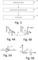
- Fig. 3 is a flow chart illustrating a method according to an embodiment.
- Fig. 3 may be implemented in the devices discussed above or below, but is not limited thereto.
- the method includes receiving a first clock signal at an interface of a device, for example together with a data signal, as explained below.
- the method comprises generating a second clock signal with variable, in particular random, delays, based on the first clock signal, as also explained above.
- the control of the variable delays for example generation of a random sequence, is performed by a controller clocked by the second clock signal (immediately at start-up, before the first variable delay is added, the second clock signal may correspond to the first clock signal)
- This second clock signal may then be used internally in the device, for example at 32 to control an RF path based on the second clock signal.
- Fig. 4A schematically shows a frequency of a digital signal like a clock signal at a frequency f 0 and its harmonics, where the logarithmic magnitude of the signal is plotted over frequency.
- BW in Fig. 4A and 4B indicates a bandwidth of an RF path like RF path 14 of Fig. 1 or a bandwidth in which antenna 20 of Fig. 2 receives and/or transmits signals.
- Fig. 4B shows the RF signal in the bandwidth BW together interference from the digital signal. As can be seen, some of the harmonics are within the bandwidth of the RF signal, thus constituting an interference, which may degrade the signal quality.
- This interference may to some extent be minimized through circuit and layout techniques that minimize the coupling effects to radio frequency path. This may include electrical and spatial separation of circuit blocks with digital signal paths from radio frequency ports on a chip level, package level or printed circuit board level.
- circuit and layout techniques that minimize the coupling effects to radio frequency path.
- This may include electrical and spatial separation of circuit blocks with digital signal paths from radio frequency ports on a chip level, package level or printed circuit board level.
- switches of Fig. 2 or any other RF path on a same chip and therefore in close proximity to a control block like building block 26, thus limiting the applicability of such techniques.
- the amplitude of the distortion at a given frequency may be reduced.
- Figures 5A to 5C illustrate the generation of second clock signal.
- first clock signal ck1 is provided to a programmable delay 50.
- Programmable delay 50 is controlled by digital control signal dctrl.
- control signal dctrl may be at least a 2-bit signal (corresponding to four possible different delays), for example a control signal with a bitwidth between 3 and 7, for example a bitwidth of 5.
- a higher bitwidth corresponding to more possible delays may lead to an improved effect regarding the distribution of interference over a broader frequency range, but on the other hand may increase an area needed for implementation.
- a bitwidth around 5 in some applications may be a good compromise between the effect achieved and the area required for implementation.
- even a 1-bit signal dctrl corresponding to two possible delays already reduces the distortion at frequencies of harmonics of the clock signal and may offer a simple implementation.
- Control signal dctrl may be changed from clock cycle to clock cycle, for example clocked by ck2.
- the delay may depend linearly on the control signal dctrl, as shown in Fig. 5C , where the delay ⁇ is plotted over the control signal value for an N-bit signal control signal dctrl, i.e. values from 0 to 2 N-1 of dctrl.
- the applied value may be generated randomly as disclosed further below, by applying a pseudo random sequence of values of length L, which may be repeated periodically.
- the linear profile of Fig. 5C is only an example, and other profile forms may also be used, for example an exponential or half-sine form. In some embodiments, such non-linear form may reduce complexity of the programmable delay circuit, may reduce power consumption or may reduce harmonic distortion caused by the programmable delay itself.
- programmable delay 50 includes a delay resistor-capacitor (RC) series circuit that is driven through an inverter.
- the inverter charges and discharges the capacitor via the series resistor during each transition on the digital signal (e.g. first clock signal ck1) applied to its input.
- the time durations needed for charging and discharging the capacitor from low-to-high and high-to-low voltage level have ideally linear dependency on the product of values of R and C, and provide the intended delay.
- the transient voltage level across the capacitor triggers the output inverter that provides the delayed clock edge of the input inverter's input signal.
- the capacitor in the RC circuit consists of capacitor banks in parallel configuration, that can be connected or disconnected from the delay RC circuit.
- each of these connections can be controlled independently through one control input bit of delay control signal dctrl, respectively. Therefore, the total capacitance in the RC circuit depends on the delay bit setting, hence the delay of the RC circuit depends on these bits as well.
- the size of the capacitor banks is increasing to the power of two: the least significant bit of dctrl switches the smallest capacitor bank with capacitance Cmin, the second bit the capacitor bank with twice Cmin, the third bit the capacitor bank with quadruple Cmin, the fourth bit 8 Cmin and so on.
- Fig. 5B shows an example behaviour of the delay ⁇ over the number of cycle i, but this sequence is only and example, and other values may be used as well.
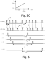
- Fig. 6 is an example showing signals provided with such a pseudo random sequence causing delays ⁇ 0 to ⁇ N-1 , and then again ⁇ 0 , i.e. according to a pseudorandom sequence having a length N-1 which is then repeated.
- a curve 60 illustrates an example clock signal without delays, with a fixed period T 0 .
- a curve 61 shows the clock signal with the delays according to the pseudo random sequence applied.
- the period length between two clock pulses varies in this case.
- the parameter c v is the attenuation of the harmonic without delay modulation
- the parameters a 0 , a v and b v are the Fourier coefficients of the square-wave first clock signal (see curve 60 of Fig. 6 ) without the variable delays, for example signal ck1.
- the harmonics Nv correspond to the harmonic distortion of the unmodulated signal.
- Fig. 11 shows results for an example implementation, where circles show values of
- in dBm without applying delays, whereas triangles show values with an applied delay signal, for a delay sequence length N 31,a duty cycle of the clock signal of 0.5, a frequency of 50MHz and a signal swing V 0 of 0.1 mV with 50 Ohm termination.
- the variable delays the peak values of
- Fig. 7 is a circuit diagram showing an example for a pseudo random bit sequence generator circuit 70 which generates pseudo random sequences of 5-bit values reg ⁇ 4:0>, which sequences are then repeated, which is usable to generate the control signal for a delay element, for example signal dctrl of Fig. 5A .
- Circuit 70 may be integrated in building block 26 of Fig. 2 or controller 13 of Fig. 1 , in particular a digital part thereof.
- Circuit 70 comprises a shift register structure including five registers 72A to 72E which are arranged in a chain, where an inverted output Q of register 72A is provided to a data input D of second register 72B, and respective non-inverted outputs Q of register 72B, 72C and 72D are provided to a respective data input D of a respective following register 72C, 72D, 72E, respectively. Furthermore, the noninverting outputs Q of registers 72B, 72E are provided to inputs of an exclusive or gate 71, and the output of exclusive or gate 71 is provided to a data input D of register 72A.
- register 72A and then non-inverted outputs Q of registers 72B to 72E form the 5 bits reg ⁇ 0> to reg ⁇ 4> of a 5-bit value reg ⁇ 4:0>, which may for example be used as signal dctrl.
- Registers 72A to 72E are clocked by a clock signal ck2, i.e. the clock signal with variable delays. In this way, in some embodiments, the operation of circuit 70 itself causes only a reduced peak interference to the RF path compared to a clocking with ck1.
- Fig. 8 shows an example sequence for control signal dctrl resulting from circuit 70 of Fig. 7 over 30 iterations, i.e. 30 clock signal cycles of signal ck2 in Fig. 7 .
- this sequence is then fed to a programmable delay like programmable delay 50 of Fig. 5A , a corresponding sequence of delays results.
- Circuit 70 is merely an example for a pseudo random sequence generator circuit, and variations or pseudo random sequence generator circuits known to the skilled person may also be used.
- an additional logic may be provided whioch detects when circuit 70 is in a state of zero (e.g. dctrl has only bits 0) and in response thereto feeds a logic 1 to the data input of first register 72A.
- Fig. 9 illustrates a device according to a further embodiment, which was used for some measurements.
- Device 90 of Fig. 9 includes eight switches 94A to 941 coupled in a single pole 4-throw (SP4T) configuration with resonance stopper as shown in Fig. 9 .
- the switches are controlled by a building block 91 receiving a first clock signal ck1 and a data signal DATA via an interface 92.
- building block 91 internally provides the first clock signal ck1 with variable delays to generate a second clock signal, which is then used internally in building block 91 and ultimately therefore to generate the signal RF control to control switches 94A to 941, which are an example for an RF path.
- a resistor 93 was added as a measurement resistor for a spectrum analyzer.
- Fig. 10 is a more detailed block diagram of a device 1000 according to an embodiment.
- Device 1000 includes a clock pad 1002 configured to receive a first clock signal ck1 and a pad 1003 configured for sending and receiving data.
- Received data dr is provided to a digital controller 1007 via a receive buffer 1005 as a buffered receive data signal datar, and data to be send datas is provided to pad 1003 as transmit data ds via a transmit buffer 1006, which is controlled by an enable signal sen.
- the interface provided at pads 1002, 1003 may be a synchronous clocked serial digital interface like a MIPI RFFE interface.
- First clock signal ck1 is provided to a programmable delay 1004, the function of which corresponds to programmable delay 50 of Fig. 5A .
- Programmable delay 1004 is controlled by digital controller 1007 via a digital control signal dctrl, which may be generated by digital controller 1007 as explained above, for example based on circuit 70 shown in Fig. 7 .
- receive buffer 1005 may also include a programmable delay, which is configured to apply the same delay to received data dr as programmable delay 1004 applies to first clock signal ck1.
- buffered receive data signal datar includes the same variable delays as second clock signal ck1. This may facilitate processing of buffered receive data signal datar by digital controller 1007, as the timing of the two signals is the same. In other embodiments, no such delays may be applied to received data signal dr. In this case, for example the delays applied to ck1 may be small enough to still allow processing of datar based on ck2 by digital controller 1007, in particular smaller than a period of clock signal ck1.
- Receive data datar may for example give instructions to device 1000 which switches in an RF block 1008 are to be opened and closed. Furthermore, digital controller 1007 may also control an analog circuit block 1009.
- An analog circuit block 1009 can include a circuit that provides process/supply voltages/temperature independent voltage/current references and DC-to-DC-conversion circuits. Examples of such circuits include bandgap reference circuits and charge pumps, but are not limited thereto.
- the voltage/current references provide stable references for the DC-to-DC-conversion circuits that generate stable biasing voltage levels for e.g. RF switching devices in RF block 1008.
- the output voltage levels of the DC-to-DC-conversion circuits could be trimmed through the digital controller signals.
- the outputs of the DC-to-DC conversion circuits could provide the opening (ON) and/or closing (OFF) voltage levels on RFcontrol signal in Fig. 9 .
- the high and/or low signal levels of RF_control signals are different from the external voltages that supply the chip.
- the translation between the digital controller signal that could be in another voltage domain as the switching devices in RF block but controls the switching devices, and the actual in analog block generated biasing voltages for proper biasing of these switching devices can be implemented through voltage level shifters, which would then be part of RF block 1008 in the example in Fig. 10 .
- transmit signal ds may be clocked by first clock signal ck1 (for example by clocking transmit buffer 1006 based on ck1), such that to the outside the interface appears to be clocked by ck1, without the second clock signal ck2 being visible to a further device communicating with device 1000.
- transmit signal ds may be clocked by second clock signal ck2, which in some implementations may reduce RF disturbance from transmit signal ds to RF circuits, as discussed above.
- it may be user configurable whether transmit signal ds is based on ck1 or ck2.
Landscapes
- Engineering & Computer Science (AREA)
- Computer Networks & Wireless Communication (AREA)
- Signal Processing (AREA)
- Physics & Mathematics (AREA)
- Nonlinear Science (AREA)
- Quality & Reliability (AREA)
- Electromagnetism (AREA)
- Pulse Circuits (AREA)
- Noise Elimination (AREA)
Abstract
Description
- The present application relates to devices and methods involving a control of a radio frequency (RF) path based on a clock signal.
- In communication systems, radio frequency signals are propagated through radio frequency paths. Such communication devices also include digital blocks which are clocked by a clock signal. For example, such digital clocks may be used as controller to control elements of the radio frequency path like switches.
- The operation of the digital block based on the clock signal acts as an interference aggressor on the radio frequency spectrum, i.e. the spectrum in the radio frequency path shows components at frequency of the clock signals and harmonics thereof. In particular, harmonics of the clock signal may be within a bandwidth used for radio frequency communication, thus reducing the quality of the actual radio frequency signal.
- A device as claimed in
claim 1 and a method as claimed inclaim 13 are provided. The dependent claims define further embodiments and an apparatus including the device. - According to an embodiment, a device is provided, comprising: an interface configured to receive a first clock signal,
- a delay circuit configured to add variable delays to the first clock signal based on a delay control signal to generate a second clock signal with variable delays,
- a controller clocked by the second clock signal and configured to generate the delay control signal; and a radio frequency path, wherein the device is configured to control the radio frequency path based on the second clock signal.
- In another embodiment, an apparatus is provided, comprising: an antenna,
- one or more tuning impedances, and
- the device as mentioned above, wherein the radio frequency path of the device is coupled to the one or more tuning impedances such that controlling the radio impedances such that controlling the radio frequency path controls tuning of the antenna by the one or more tuning impedances.
- In another embodiment, a method is provided, comprising: receiving, at an interface, a first clock signal,
- adding variable delays to the first clock signal based on a delay control signal to generate a second clock signal with variable delays,
- generating the delay control signal with a controller clocked by the second clock signal; and
- controlling a radio frequency path based on the second clock signal.
- The above gives merely a brief overview and is not to be construed as limiting, as other embodiments may include different features than the ones given above.
-
-
Fig. 1 is a block diagram of a device according to an embodiment. -
Fig. 2 is a diagram illustrating an apparatus according to an embodiment. -
Fig. 3 is a flowchart illustrating a method according to an embodiment. -
Figures 4A and 4B are explanatory diagrams for explaining interference from a digital block to a radio frequency path. -
Fig. 5A is a diagram illustrating introduction of variable delays to a clock circuit, andFigures 5B and5C are diagrams illustrating the operation ofFig. 5A . -
Fig. 6 is a signal diagram for explaining various embodiments. -
Fig. 7 is a circuit diagram of a circuit generating random numbers usable as delay control signal in some embodiments. -
Fig. 8 is a diagram illustrating operation of the circuit ofFig. 7 . -
Fig. 9 is a circuit diagram of a device according to some embodiments. -
Fig. 10 is a block diagram of a device according to an embodiment. -
Fig. 11 is an example graph illustrating the effects of some embodiments. - In the following, various embodiments will be described in detail referring to the attached drawings. These embodiments are given as examples only and are not to be construed as limiting. For example, while embodiments may be described as comprising a plurality of features (for example components, elements, acts, events, steps etc.), in other embodiments some of these features may be omitted or replaced by alternative features. In addition to the features explicitly shown and described, additional features may be provided, for example features used in conventional radio frequency devices. Such conventional features will not be described in detail.
- Variations, modifications and details described with respect to one of the embodiments may also be applied to other embodiments and therefore will not be described repeatedly. Features from different embodiments may be combined to form further embodiments.
- Any connections or couplings between elements shown in the drawings or described herein are electrical connections or couplings unless noted otherwise. Such connections or couplings may be modified, for example by adding or removing elements, as long as the general purpose of the connection or coupling, for example to transmit a certain signal, to provide a current and/or voltage, to provide a control etc. is essentially maintained.
- Turning now to the drawings,
Fig. 1 is a block diagram of adevice 10 according to an embodiment. -
Device 10 ofFig. 1 includes aninterface 11, which is configured to receive a clock signal ck1 from an external entity. For example, clock signal ck1 may be a clock signal used in an apparatus in whichdevice 10 is provided.Interface 11, in addition to receiving clock interface ck1, may also be used to receive and/or send a data signal clocked by clock signal ck1, as will be explained further below with reference toFig. 10 . In some embodiments,interface 11 may be a synchronous clocked digital serial interface like a MIPI RFFE interface, but is not limited thereto. - Clock signal ck1 is provided to a
controller 13, which may include digital circuitry, analog circuitry or both. In particular, clock signal ck1 is provided to adelay circuit 15 ofcontroller 13.Delay circuit 15 is configured to add variable delays to clock signal ck1, in particular variable random delays, to generate a clock signal ck2 with variable delays.Delay circuit 15 is controlled bycontroller 13. For example,controller 13 may provide a delay control signal based on a random sequence to delaycircuit 15. In turn, in embodiments discussed herein,controller 13, for example to generate the delay control signal, is clocked by second clock signal ck2. The term "random sequence" as used herein also includes pseudorandom sequences, i.e. sequences that appear random, but are generated for example by a circuit which operates in a deterministic manner. The same applies to other uses of the term "random"; also here "pseudorandom" is intended to be included, e.g. in random delays. In other embodiments, a predefined sequence not generated by a pseudorandom sequences generator or the like may be used. - The concept of variable, in particular random, delays will be described in further detail further below with reference to
Figures 5A to 5C and6 . In such a clock signal with variable delays, for example each clock pulse, each rising edge, each falling edge or both rising and falling edge may be delayed by a random delay. - In some embodiments, second clock signals ck2 is used internally within
device 10, whereas for external communication, for example viainterface 11, first clock signals ck1 is used. Therefore, second clock signal ck2 in some embodiments is "hidden" to the world outsidedevice 10, such that other devices may communicate and treatdevice 10 as a device operating on a normal clock signal, i.e. first clock signal ck1, without such variable delays. However, forexample controller 13 may operate based on second clock signal ck2, anddevice 10 may in particular control a radio frequency path (RF path) between afirst node 14A and asecond node 14B based on second clock signal ck2. ControllingRF path 14 may for example include controlling switches ofRF path 14, for example for tuning purposes, or controlling other elements inRF path 14 like adjustable, e.g. tuneable or switchable amplifiers, capacitors and inductors, oscillators, mixers, phase locked loops (PLLs), resonators, filters or other elements that have settings, as will be explained below using examples. - In some embodiments, by using second clock signal ck2 with variable delays, an impact of interference from
controller 13 to radio frequency parts of an apparatus or system, includingradio frequency path 14 and signals transmitted therein, may be reduced. For example, contributions of harmonics of second clock signal ck2 inradio frequency path 14 or other radio frequency circuits outsidedevice 10 may be "smeared out", i.e. distributed with a lesser amplitude over a wider frequency range, such that forindividual frequencies device 10 has less impact on radio frequency signals. This also will be explained further below in more detail. -
Fig. 2 is a diagram including an apparatus according to an embodiment, that comprises adevice 27 according to an embodiment. The apparatus ofFig. 2 may for example be part of a mobile communication device and includes anantenna 20 to which for example signals to be transmitted may be provided via aline 21, and/or received signals may be tapped vialine 21, as in conventional communication devices. - For tuning purposes, a node of
antenna 20 is coupled to aninductor 22 and acapacitor 23 as shown. Via aswitch 24 ofdevice 27,capacitor 23 may selectively be coupled to ground, and via aswitch 25 ofdevice 27,inductor 22 may be selectively coupled to ground.Switches RF path 14 ofFig. 1 , included indevice 27. - Furthermore,
device 27 includes abuilding block 26 which may include analog and digital circuitry and which receives at least a clock signal and a data signal via aninterface 28. The data signal is clocked by the clock signal and for example indicates which ofswitches block 26 includes a variable delay circuit and a controller as discussed with reference toFig. 1 fordelay circuit 13, to provide the clock signal received atinterface 28 with variable delays. Internally,building block 26 then operates on the clock signal with variable delays, corresponding to second clock signal ck2 ofFig. 1 , and e.g. operatesswitches arrow 28 inFig. 2 as frequency contributions for example of harmonics of the clock signal may be spread out over a wider frequency range with lower intensity. - Building
block 26 may also transmit signals viainterface 28, based on the clock signal received, and not based on the clock signal with variable delays, such that in communications viainterface 28 the clock signal with variable delays is not used. - The configuration with two single pole single throw switches in
Fig. 2 (switches 24, 25)is merely an example for an RF path, and other elements then switches or other switch configurations, for example configurations conventionally used in antenna or RF tuning applications, may also be used. -
Fig. 3 is a flow chart illustrating a method according to an embodiment. - The method of
Fig. 3 may be implemented in the devices discussed above or below, but is not limited thereto. - At 30, the method includes receiving a first clock signal at an interface of a device, for example together with a data signal, as explained below.
- At 31, the method comprises generating a second clock signal with variable, in particular random, delays, based on the first clock signal, as also explained above. The control of the variable delays, for example generation of a random sequence, is performed by a controller clocked by the second clock signal (immediately at start-up, before the first variable delay is added, the second clock signal may correspond to the first clock signal) This second clock signal may then be used internally in the device, for example at 32 to control an RF path based on the second clock signal.
- Next, the concept of mitigating radio frequency disturbances using variable delays will be explained in some more detail.
-
Fig. 4A schematically shows a frequency of a digital signal like a clock signal at a frequency f0 and its harmonics, where the logarithmic magnitude of the signal is plotted over frequency. Generally, the magnitude |U(v)| of harmonic v for an ideal square-wave clock signal waveform having instantaneous edges (no transition time between high and low signal levels) may be calculated for a square-wave signal with instantaneous transitions (edges) through a Fourier series as
Fig. 4A and 4B indicates a bandwidth of an RF path likeRF path 14 ofFig. 1 or a bandwidth in whichantenna 20 ofFig. 2 receives and/or transmits signals. -
Fig. 4B shows the RF signal in the bandwidth BW together interference from the digital signal. As can be seen, some of the harmonics are within the bandwidth of the RF signal, thus constituting an interference, which may degrade the signal quality. - This interference may to some extent be minimized through circuit and layout techniques that minimize the coupling effects to radio frequency path. This may include electrical and spatial separation of circuit blocks with digital signal paths from radio frequency ports on a chip level, package level or printed circuit board level. However, with increasing integration, it is for example desirable to have the switches of
Fig. 2 or any other RF path on a same chip and therefore in close proximity to a control block like buildingblock 26, thus limiting the applicability of such techniques. By introducing variable delays, the amplitude of the distortion at a given frequency may be reduced. -
Figures 5A to 5C illustrate the generation of second clock signal. InFig. 5A , first clock signal ck1 is provided to aprogrammable delay 50.Programmable delay 50 is controlled by digital control signal dctrl. In some embodiments, control signal dctrl may be at least a 2-bit signal (corresponding to four possible different delays), for example a control signal with a bitwidth between 3 and 7, for example a bitwidth of 5. Generally, a higher bitwidth corresponding to more possible delays may lead to an improved effect regarding the distribution of interference over a broader frequency range, but on the other hand may increase an area needed for implementation. A bitwidth around 5 in some applications may be a good compromise between the effect achieved and the area required for implementation. However, even a 1-bit signal dctrl corresponding to two possible delays (including the possibility of either a predefined delay or no delay) in some embodiments already reduces the distortion at frequencies of harmonics of the clock signal and may offer a simple implementation. -
Programmable delay 50 then outputs second clock signal ck2. Control signal dctrl may be changed from clock cycle to clock cycle, for example clocked by ck2. In some embodiments, the delay may depend linearly on the control signal dctrl, as shown inFig. 5C , where the delay τ is plotted over the control signal value for an N-bit signal control signal dctrl, i.e. values from 0 to 2N-1 of dctrl. The applied value may be generated randomly as disclosed further below, by applying a pseudo random sequence of values of length L, which may be repeated periodically. It should be noted that the linear profile ofFig. 5C is only an example, and other profile forms may also be used, for example an exponential or half-sine form. In some embodiments, such non-linear form may reduce complexity of the programmable delay circuit, may reduce power consumption or may reduce harmonic distortion caused by the programmable delay itself. - One implementation example of
programmable delay 50 includes a delay resistor-capacitor (RC) series circuit that is driven through an inverter. The inverter charges and discharges the capacitor via the series resistor during each transition on the digital signal (e.g. first clock signal ck1) applied to its input. The time durations needed for charging and discharging the capacitor from low-to-high and high-to-low voltage level have ideally linear dependency on the product of values of R and C, and provide the intended delay. The transient voltage level across the capacitor triggers the output inverter that provides the delayed clock edge of the input inverter's input signal. The capacitor in the RC circuit consists of capacitor banks in parallel configuration, that can be connected or disconnected from the delay RC circuit. Each of these connections can be controlled independently through one control input bit of delay control signal dctrl, respectively. Therefore, the total capacitance in the RC circuit depends on the delay bit setting, hence the delay of the RC circuit depends on these bits as well. In case of the linear delay profile discussed with respect toFig. 5C above, the size of the capacitor banks is increasing to the power of two: the least significant bit of dctrl switches the smallest capacitor bank with capacitance Cmin, the second bit the capacitor bank with twice Cmin, the third bit the capacitor bank with quadruple Cmin, the fourth bit 8 Cmin and so on. -
Fig. 5B shows an example behaviour of the delay τ over the number of cycle i, but this sequence is only and example, and other values may be used as well. -
Fig. 6 is an example showing signals provided with such a pseudo random sequence causing delays τ0 to τN-1, and then again τ0, i.e. according to a pseudorandom sequence having a length N-1 which is then repeated. Acurve 60 illustrates an example clock signal without delays, with a fixed period T0. A curve 61 shows the clock signal with the delays according to the pseudo random sequence applied. As can be seen, the period length between two clock pulses varies in this case. However, as shown in the curves labelled i=0 to i=N-1, the period length between two pulses modulated with the same delay (τ0 for i=0, τ1 for i=1... τN-1 for i=N-1) still is N × T0. - In contrast to the magnitude according to equation (1) above for a signal without the delays applied, the magnitude |U(v)| of harmonic v after the application of the delay is calculated according to:


modulation 
- The parameters a0, av and bv are the Fourier coefficients of the square-wave first clock signal (see
curve 60 ofFig. 6 ) without the variable delays, for example signal ck1. The harmonics Nv correspond to the harmonic distortion of the unmodulated signal.Fig. 11 shows results for an example implementation, where circles show values of |U(v)| in dBm without applying delays, whereas triangles show values with an applied delay signal, for a delay sequence length N=31,a duty cycle of the clock signal of 0.5, a frequency of 50MHz and a signal swing V0 of 0.1 mV with 50 Ohm termination. As can be seen, by applying the variable delays, the peak values of |U(v)| are reduced significantly, for example in the order of 10 dB, even if additional contributions occur in sidebands due to the "smearing out" of the disturbance. -
Fig. 7 is a circuit diagram showing an example for a pseudo random bitsequence generator circuit 70 which generates pseudo random sequences of 5-bit values reg <4:0>, which sequences are then repeated, which is usable to generate the control signal for a delay element, for example signal dctrl ofFig. 5A .Circuit 70 may be integrated inbuilding block 26 ofFig. 2 orcontroller 13 ofFig. 1 , in particular a digital part thereof. -
Circuit 70 comprises a shift register structure including fiveregisters 72A to 72E which are arranged in a chain, where an inverted outputQ ofregister 72A is provided to a data input D ofsecond register 72B, and respective non-inverted outputs Q ofregister 72B, 72C and 72D are provided to a respective data input D of a respective followingregister 72C, 72D, 72E, respectively. Furthermore, the noninverting outputs Q ofregisters gate 71, and the output of exclusive orgate 71 is provided to a data input D ofregister 72A. - The inverted output
Q ofregister 72A and then non-inverted outputs Q ofregisters 72B to 72E form the 5 bits reg<0> to reg<4> of a 5-bit value reg<4:0>, which may for example be used as signal dctrl.Registers 72A to 72E are clocked by a clock signal ck2, i.e. the clock signal with variable delays. In this way, in some embodiments, the operation ofcircuit 70 itself causes only a reduced peak interference to the RF path compared to a clocking with ck1. -
Fig. 8 shows an example sequence for control signal dctrl resulting fromcircuit 70 ofFig. 7 over 30 iterations, i.e. 30 clock signal cycles of signal ck2 inFig. 7 . When this sequence is then fed to a programmable delay likeprogrammable delay 50 ofFig. 5A , a corresponding sequence of delays results. -
Circuit 70 is merely an example for a pseudo random sequence generator circuit, and variations or pseudo random sequence generator circuits known to the skilled person may also be used. For instance, incircuit 70, an additional logic may be provided whioch detects whencircuit 70 is in a state of zero (e.g. dctrl has only bits 0) and in response thereto feeds alogic 1 to the data input offirst register 72A. -
Fig. 9 illustrates a device according to a further embodiment, which was used for some measurements. -
Device 90 ofFig. 9 includes eightswitches 94A to 941 coupled in a single pole 4-throw (SP4T) configuration with resonance stopper as shown inFig. 9 . The switches are controlled by abuilding block 91 receiving a first clock signal ck1 and a data signal DATA via aninterface 92. As explained previously,building block 91 internally provides the first clock signal ck1 with variable delays to generate a second clock signal, which is then used internally inbuilding block 91 and ultimately therefore to generate the signal RFcontrol to controlswitches 94A to 941, which are an example for an RF path. For measurement purposes, instead for example of an antenna for tuning purposes aresistor 93 was added as a measurement resistor for a spectrum analyzer. - Also in this arrangement, measurements have shown a suppression of spurious tones having high magnitude, for example by 10 dBm, while sidebands occur due to the "smearing out".
-
Fig. 10 is a more detailed block diagram of adevice 1000 according to an embodiment.Device 1000 includes aclock pad 1002 configured to receive a first clock signal ck1 and apad 1003 configured for sending and receiving data. Received data dr is provided to adigital controller 1007 via a receivebuffer 1005 as a buffered receive data signal datar, and data to be send datas is provided to pad 1003 as transmit data ds via a transmitbuffer 1006, which is controlled by an enable signal sen. In some embodiments, the interface provided atpads - First clock signal ck1 is provided to a
programmable delay 1004, the function of which corresponds toprogrammable delay 50 ofFig. 5A .Programmable delay 1004 is controlled bydigital controller 1007 via a digital control signal dctrl, which may be generated bydigital controller 1007 as explained above, for example based oncircuit 70 shown inFig. 7 . - In some embodiments, receive
buffer 1005 may also include a programmable delay, which is configured to apply the same delay to received data dr asprogrammable delay 1004 applies to first clock signal ck1. In this case, buffered receive data signal datar includes the same variable delays as second clock signal ck1. This may facilitate processing of buffered receive data signal datar bydigital controller 1007, as the timing of the two signals is the same. In other embodiments, no such delays may be applied to received data signal dr. In this case, for example the delays applied to ck1 may be small enough to still allow processing of datar based on ck2 bydigital controller 1007, in particular smaller than a period of clock signal ck1. - Receive data datar may for example give instructions to
device 1000 which switches in anRF block 1008 are to be opened and closed. Furthermore,digital controller 1007 may also control ananalog circuit block 1009. - An
analog circuit block 1009 can include a circuit that provides process/supply voltages/temperature independent voltage/current references and DC-to-DC-conversion circuits. Examples of such circuits include bandgap reference circuits and charge pumps, but are not limited thereto. The voltage/current references provide stable references for the DC-to-DC-conversion circuits that generate stable biasing voltage levels for e.g. RF switching devices inRF block 1008. The output voltage levels of the DC-to-DC-conversion circuits could be trimmed through the digital controller signals. The outputs of the DC-to-DC conversion circuits could provide the opening (ON) and/or closing (OFF) voltage levels on RFcontrol signal inFig. 9 . In this case, the high and/or low signal levels of RF_control signals are different from the external voltages that supply the chip. The translation between the digital controller signal that could be in another voltage domain as the switching devices in RF block but controls the switching devices, and the actual in analog block generated biasing voltages for proper biasing of these switching devices can be implemented through voltage level shifters, which would then be part ofRF block 1008 in the example inFig. 10 . - In some embodiments, transmit signal ds may be clocked by first clock signal ck1 (for example by clocking transmit
buffer 1006 based on ck1), such that to the outside the interface appears to be clocked by ck1, without the second clock signal ck2 being visible to a further device communicating withdevice 1000. In other embodiments, transmit signal ds may be clocked by second clock signal ck2, which in some implementations may reduce RF disturbance from transmit signal ds to RF circuits, as discussed above. In still other embodiments, it may be user configurable whether transmit signal ds is based on ck1 or ck2. - Some embodiments are defined by the following examples:
- Example 1. A device, comprising:
- an interface configured to receive a first clock signal,
- a delay circuit configured to add variable delays to the first clock signal based on a delay control signal to generate a second clock signal with variable delays,
- a controller clocked by the second clock signal and configured to generate the delay control signal, and
- a radio frequency path, wherein the device is configured to control the radio frequency path based on the second clock signal.
- Example 2. The device of example 1, wherein the delay circuit is configured to delay at least one edge of each of a plurality of clock pulses of the first clock signal according to the delay control signal, wherein the delay control signal indicates a random delay sequence.
- Example 3. The device of example 2, wherein the random delay sequence has a length L and is repeated periodically.
- Example 4. The device of example 2 or 3, wherein the delay circuit comprises a programmable delay element, and wherein the controller comprises a random sequence generator circuit configured to generate the delay control signal clocked by the second clock signal.
- Example 5. The device of example 4, wherein the random sequence generator circuit is configured to generate digital random values with a bitwidth equal to or greater than 2.
- Example 6. The device of example 5, wherein the bitwidth is between 3 and 7.
- Example 7. The device of any one of examples 1 to 6, wherein each of the variable delays is smaller than a period length of the first clock signal.
- Example 8. The device of any one of examples 1 to 7, wherein the radio frequency path includes one or more radio frequency switches, and wherein, to control the radio frequency path, the device is configured to control the one or more radio frequency switches.
- Example 9. The device of any one of examples 1 to 8, wherein the interface is further configure to receive a data signal, wherein the device is configured to control the radio frequency path further based on the received data signal.
- Example 10. The device of example 9, further comprising a further delay circuit configured to add variable delays to the received data signal corresponding to the variable delays added to the first clock signal, to generate a further received data signal with variable delays.
- Example 11. The device of example 9 or 10, wherein the interface comprises a synchronous clocked serial digital interface.
- Example 12. The device of example 11, wherein the interface is a MIPI RFFE interface.
- Example 13. The device of any one of examples 1 to 12, wherein the device is further configured to send transmit data over the interface based on the first clock signal.
- Example 14. The device of example 13, wherein the device is configured to configurably send the transmit data either based on the first clock signal or based on the second clock signal.
- Example 15. An apparatus, comprising:
- an antenna,
- one or more tuning impedances, and
- the device of any one of examples 1 to 14, wherein the radio frequency path of the device is coupled to the one or more tuning impedances such that controlling the radio frequency path controls tuning of the antenna by the one or more tuning impedances.
- Example 16. A method, comprising:
- receiving, at an interface, a first clock signal,
- adding variable delays to the first clock signal based on a delay control signal to generate a second clock signal with variable delays,
- generating the delay control signal with a controller clocked by the second clock signal ; and
- controlling a radio frequency path based on the second clock signal.
- Example 17. The method of example 16, wherein adding variable delays comprises delaying at least one edge of each of a plurality of clock pulses of the first clock signal according to the delay control signal, wherein the delay control signal indicates a random delay sequence.
- Example 18. The method of example 17, further comprising generating the delay control signal using a random sequence generator circuit clocked by the second clock signal.
- Example 19. The method of any one of examples 16 to 18, further comprising receiving a data signal,
- adding variable delays to the received data signal corresponding to the variable delays added to the first clock signal, to generate a further received data signal with variable delays, and
- controlling the radio frequency path based on the further received data signal.
- Although specific embodiments have been illustrated and described herein, it will be appreciated by those of ordinary skill in the art that a variety of alternate and/or equivalent implementations may be substituted for the specific embodiments shown and described without departing from the scope of the present invention. This application is intended to cover any adaptations or variations of the specific embodiments discussed herein. Therefore, it is intended that this invention be limited only by the claims and the equivalents thereof.
Claims (15)
- A device (10; 27; 90; 1000), comprising:an interface (11; 28; 92) configured to receive a first clock signal (ck1),a delay circuit (13; 50; 1004) configured to add variable delays to the first clock signal (ck1) based on a delay control signal (dctrl) to generate a second clock signal (ck2) with variable delays,a controller (12; 1007) clocked by the second clock signal (ck2) and configured to generate the delay control signal (dctrl), anda radio frequency path (14), wherein the device (10; 27; 90; 100) is configured to control the radio frequency path (14) based on the second clock signal (ck2).
- The device (10; 27; 90; 100) of claim 1, wherein the delay circuit (13; 50; 1004) is configured to delay at least one edge of each of a plurality of clock pulses of the first clock signal (ck1) according to the delay control signal (dctrl), wherein the delay control signal (dctrl) indicates a random delay sequence.
- The device (10; 27; 90; 100) of claim 2, wherein the random delay sequence has a length L and is repeated periodically.
- The device (10; 27; 90; 100) of claim 2 or 3, wherein the delay circuit (13; 50; 1004) comprises a programmable delay element, and wherein the controller (12; 1007) comprises a random sequence generator circuit (70) configured to generate the delay control signal (dctrl) clocked by the second clock signal (ck2).
- The device (10; 27; 90; 100) of any one of claims 1 to 4, wherein each of the variable delays is smaller than a period length of the first clock signal (ck1).
- The device (10; 27; 90; 100) of any one of claims 1 to 5, wherein the radio frequency path (14) includes one or more radio frequency switches (24, 25; 94A-94I), and wherein, to control the radio frequency path (14), the device (10; 27; 90; 100) is configured to control the one or more radio frequency switches (24, 25; 94A-94I).
- The device (10; 27; 90; 100) of any one of claims 1 to 6, wherein the interface (11; 28; 92) is further configure to receive a data signal (dr), wherein the device (10; 27; 90; 100) is configured to control the radio frequency path (14) further based on the received data signal (dr).
- The device of claim 7, further comprising a further delay circuit (1005) configured to add variable delays to the received data signal (dr) corresponding to the variable delays added to the first clock signal, to generate a further received data signal (datar) with variable delays.
- The device (10; 27; 90; 100) of claim 7 or 8, wherein the interface (11; 28; 92) comprises a synchronous clocked serial digital interface.
- The device (10; 27; 90; 100) of any one of claims 1 to 9, wherein the device (10; 27; 90; 100) is further configured to send transmit data (ds) over the interface (11; 28; 92) based on the first clock signal (ck1).
- The device of claim 10, wherein the device is configured to configurably send the transmit data either based on the first clock signal (ck1) or based on the second clock signal (ck2) .
- An apparatus, comprising:an antenna,one or more tuning impedances, andthe device (10; 27; 90; 100) of any one of claims 1 to 11,wherein the radio frequency path (14) of the device (10; 27; 90; 100) is coupled to the one or more tuning impedances such that controlling the radio frequency path (14) controls tuning of the antenna by the one or more tuning impedances.
- A method, comprising:receiving, at an interface (11; 28; 92), a first clock signal (ck1),adding variable delays to the first clock signal (ck1) based on a delay control signal (dctrl) to generate a second clock signal (ck2) with variable delays,generating the delay control signal (dctrl) with a controller (12; 1007) clocked by the second clock signal (ck2); and controlling a radio frequency path (14) based on the second clock signal (ck2).
- The method of claim 13, wherein adding variable delays comprises delaying at least one edge of each of a plurality of clock pulses of the first clock signal (ck1) according to the delay control signal (dctrl), wherein the delay control signal (dctrl) indicates a random delay sequence.
- The method of claim 14, further comprising generating the delay control signal (dctrl) using a random sequence generator circuit (70) clocked by the second clock signal (ck2).
Priority Applications (3)
| Application Number | Priority Date | Filing Date | Title |
|---|---|---|---|
| EP22208809.8A EP4376217A1 (en) | 2022-11-22 | 2022-11-22 | Devices and methods controlling a radio frequency path |
| US18/503,765 US20240171210A1 (en) | 2022-11-22 | 2023-11-07 | Devices and methods controlling a radio frequency path |
| CN202311562467.0A CN118074744A (en) | 2022-11-22 | 2023-11-22 | Device and method for controlling radio frequency path |
Applications Claiming Priority (1)
| Application Number | Priority Date | Filing Date | Title |
|---|---|---|---|
| EP22208809.8A EP4376217A1 (en) | 2022-11-22 | 2022-11-22 | Devices and methods controlling a radio frequency path |
Publications (1)
| Publication Number | Publication Date |
|---|---|
| EP4376217A1 true EP4376217A1 (en) | 2024-05-29 |
Family
ID=84361427
Family Applications (1)
| Application Number | Title | Priority Date | Filing Date |
|---|---|---|---|
| EP22208809.8A Pending EP4376217A1 (en) | 2022-11-22 | 2022-11-22 | Devices and methods controlling a radio frequency path |
Country Status (3)
| Country | Link |
|---|---|
| US (1) | US20240171210A1 (en) |
| EP (1) | EP4376217A1 (en) |
| CN (1) | CN118074744A (en) |
Citations (3)
| Publication number | Priority date | Publication date | Assignee | Title |
|---|---|---|---|---|
| GB2493026A (en) * | 2011-07-22 | 2013-01-23 | Nvidia Corp | Method of spreading a clock signal using a variable delay |
| EP3016200A1 (en) * | 2014-10-29 | 2016-05-04 | MediaTek Singapore Pte Ltd. | Integrated circuit, wireless communication unit, and method for antenna matching |
| WO2018132216A1 (en) * | 2017-01-13 | 2018-07-19 | Qualcomm Incorporated | Protection system for radio frequency switches |
Family Cites Families (1)
| Publication number | Priority date | Publication date | Assignee | Title |
|---|---|---|---|---|
| US7706759B2 (en) * | 2007-01-30 | 2010-04-27 | Broadcom Corporation | RF reception system with programmable impedance matching networks and methods for use therewith |
-
2022
- 2022-11-22 EP EP22208809.8A patent/EP4376217A1/en active Pending
-
2023
- 2023-11-07 US US18/503,765 patent/US20240171210A1/en active Pending
- 2023-11-22 CN CN202311562467.0A patent/CN118074744A/en active Pending
Patent Citations (3)
| Publication number | Priority date | Publication date | Assignee | Title |
|---|---|---|---|---|
| GB2493026A (en) * | 2011-07-22 | 2013-01-23 | Nvidia Corp | Method of spreading a clock signal using a variable delay |
| EP3016200A1 (en) * | 2014-10-29 | 2016-05-04 | MediaTek Singapore Pte Ltd. | Integrated circuit, wireless communication unit, and method for antenna matching |
| WO2018132216A1 (en) * | 2017-01-13 | 2018-07-19 | Qualcomm Incorporated | Protection system for radio frequency switches |
Also Published As
| Publication number | Publication date |
|---|---|
| CN118074744A (en) | 2024-05-24 |
| US20240171210A1 (en) | 2024-05-23 |
Similar Documents
| Publication | Publication Date | Title |
|---|---|---|
| Roza | Analog-to-digital conversion via duty-cycle modulation | |
| US8004330B1 (en) | Reduction of electromagnetic interference for differential signals | |
| US4816830A (en) | Waveform shaping apparatus and method | |
| US9397647B2 (en) | Clock spurs reduction technique | |
| Zhu et al. | Distributed waveform generator: A new circuit technique for ultra-wideband pulse generation, shaping and modulation | |
| KR100925364B1 (en) | Clock modulation circuit for correcting the duty ratio, and spread spectrum clock generator comprising the same | |
| EP4142157A1 (en) | A low intermediate frequency transmitter | |
| JP4179568B2 (en) | Spread spectrum phase modulation for electromagnetic interference suppression in parallel data channels | |
| Demirkan et al. | A pulse-based ultra-wideband transmitter in 90-nm CMOS for WPANs | |
| TW201841469A (en) | Pulse Generator | |
| US10637483B2 (en) | Neutralization of phase perturbations from deterministic electromagnetic interference | |
| US20040096020A1 (en) | EMI cancellation method and system | |
| JP2510413B2 (en) | Transversal filter | |
| US4603301A (en) | Amplitude insensitive delay lines in a frequency modulated signal detector | |
| US20240171210A1 (en) | Devices and methods controlling a radio frequency path | |
| EP1330658B1 (en) | Bist method for testing cut-off frequency of low-pass filters | |
| US20110241747A1 (en) | Apparatus and method for reducing interference signals in an integrated circuit using multiphase clocks | |
| US20090219064A1 (en) | Pulse generator circuit and communication apparatus | |
| US7855589B2 (en) | Pulse generator circuit and communication apparatus | |
| EP1505732B1 (en) | Digital clock modulator | |
| US5200648A (en) | Emulator circuit and method for generating CMOS level clock input | |
| KR20170139491A (en) | Circuits and methods for transceiver self-interference cancellers | |
| JP2005535991A (en) | Shift register circuit arrangement with improved compatibility and method of operation thereof | |
| Kord | Magnetless circulators based on linear time-varying circuits | |
| Tsymbal et al. | SPREAD SPECTRUM MODULATION TECHNIQUE INVESTIGATION FOR PLL LESS CLOCK GENERATOR USING MATLAB/SIMULINK ENVIRONMENT |
Legal Events
| Date | Code | Title | Description |
|---|---|---|---|
| PUAI | Public reference made under article 153(3) epc to a published international application that has entered the european phase |
Free format text: ORIGINAL CODE: 0009012 |
|
| STAA | Information on the status of an ep patent application or granted ep patent |
Free format text: STATUS: THE APPLICATION HAS BEEN PUBLISHED |
|
| AK | Designated contracting states |
Kind code of ref document: A1 Designated state(s): AL AT BE BG CH CY CZ DE DK EE ES FI FR GB GR HR HU IE IS IT LI LT LU LV MC ME MK MT NL NO PL PT RO RS SE SI SK SM TR |
|
| STAA | Information on the status of an ep patent application or granted ep patent |
Free format text: STATUS: REQUEST FOR EXAMINATION WAS MADE |
|
| 17P | Request for examination filed |
Effective date: 20241127 |
|
| RBV | Designated contracting states (corrected) |
Designated state(s): AL AT BE BG CH CY CZ DE DK EE ES FI FR GB GR HR HU IE IS IT LI LT LU LV MC ME MK MT NL NO PL PT RO RS SE SI SK SM TR |