EP4376092A1 - Ic structure with gate electrode fully within v-shaped cavity - Google Patents
Ic structure with gate electrode fully within v-shaped cavity Download PDFInfo
- Publication number
- EP4376092A1 EP4376092A1 EP23201745.9A EP23201745A EP4376092A1 EP 4376092 A1 EP4376092 A1 EP 4376092A1 EP 23201745 A EP23201745 A EP 23201745A EP 4376092 A1 EP4376092 A1 EP 4376092A1
- Authority
- EP
- European Patent Office
- Prior art keywords
- shaped cavity
- spacers
- gate electrode
- gate
- dielectric layer
- Prior art date
- Legal status (The legal status is an assumption and is not a legal conclusion. Google has not performed a legal analysis and makes no representation as to the accuracy of the status listed.)
- Pending
Links
Images

Classifications
-
- H—ELECTRICITY
- H10—SEMICONDUCTOR DEVICES; ELECTRIC SOLID-STATE DEVICES NOT OTHERWISE PROVIDED FOR
- H10D—INORGANIC ELECTRIC SEMICONDUCTOR DEVICES
- H10D64/00—Electrodes of devices having potential barriers
- H10D64/20—Electrodes characterised by their shapes, relative sizes or dispositions
- H10D64/27—Electrodes not carrying the current to be rectified, amplified, oscillated or switched, e.g. gates
- H10D64/311—Gate electrodes for field-effect devices
- H10D64/411—Gate electrodes for field-effect devices for FETs
- H10D64/511—Gate electrodes for field-effect devices for FETs for IGFETs
- H10D64/512—Disposition of the gate electrodes, e.g. buried gates
- H10D64/513—Disposition of the gate electrodes, e.g. buried gates within recesses in the substrate, e.g. trench gates, groove gates or buried gates
-
- H—ELECTRICITY
- H10—SEMICONDUCTOR DEVICES; ELECTRIC SOLID-STATE DEVICES NOT OTHERWISE PROVIDED FOR
- H10D—INORGANIC ELECTRIC SEMICONDUCTOR DEVICES
- H10D30/00—Field-effect transistors [FET]
- H10D30/01—Manufacture or treatment
- H10D30/021—Manufacture or treatment of FETs having insulated gates [IGFET]
-
- H—ELECTRICITY
- H10—SEMICONDUCTOR DEVICES; ELECTRIC SOLID-STATE DEVICES NOT OTHERWISE PROVIDED FOR
- H10D—INORGANIC ELECTRIC SEMICONDUCTOR DEVICES
- H10D30/00—Field-effect transistors [FET]
- H10D30/60—Insulated-gate field-effect transistors [IGFET]
-
- H—ELECTRICITY
- H10—SEMICONDUCTOR DEVICES; ELECTRIC SOLID-STATE DEVICES NOT OTHERWISE PROVIDED FOR
- H10D—INORGANIC ELECTRIC SEMICONDUCTOR DEVICES
- H10D62/00—Semiconductor bodies, or regions thereof, of devices having potential barriers
- H10D62/10—Shapes, relative sizes or dispositions of the regions of the semiconductor bodies; Shapes of the semiconductor bodies
- H10D62/117—Shapes of semiconductor bodies
-
- H—ELECTRICITY
- H10—SEMICONDUCTOR DEVICES; ELECTRIC SOLID-STATE DEVICES NOT OTHERWISE PROVIDED FOR
- H10D—INORGANIC ELECTRIC SEMICONDUCTOR DEVICES
- H10D62/00—Semiconductor bodies, or regions thereof, of devices having potential barriers
- H10D62/10—Shapes, relative sizes or dispositions of the regions of the semiconductor bodies; Shapes of the semiconductor bodies
- H10D62/13—Semiconductor regions connected to electrodes carrying current to be rectified, amplified or switched, e.g. source or drain regions
- H10D62/149—Source or drain regions of field-effect devices
- H10D62/151—Source or drain regions of field-effect devices of IGFETs
-
- H—ELECTRICITY
- H10—SEMICONDUCTOR DEVICES; ELECTRIC SOLID-STATE DEVICES NOT OTHERWISE PROVIDED FOR
- H10D—INORGANIC ELECTRIC SEMICONDUCTOR DEVICES
- H10D64/00—Electrodes of devices having potential barriers
- H10D64/01—Manufacture or treatment
-
- H—ELECTRICITY
- H10—SEMICONDUCTOR DEVICES; ELECTRIC SOLID-STATE DEVICES NOT OTHERWISE PROVIDED FOR
- H10D—INORGANIC ELECTRIC SEMICONDUCTOR DEVICES
- H10D64/00—Electrodes of devices having potential barriers
- H10D64/01—Manufacture or treatment
- H10D64/013—Manufacture or treatment of electrodes having a conductor capacitively coupled to a semiconductor by an insulator
- H10D64/01302—Manufacture or treatment of electrodes having a conductor capacitively coupled to a semiconductor by an insulator the insulator being formed after the semiconductor body, the semiconductor being silicon
- H10D64/01304—Manufacture or treatment of electrodes having a conductor capacitively coupled to a semiconductor by an insulator the insulator being formed after the semiconductor body, the semiconductor being silicon characterised by the conductor
- H10D64/01324—Manufacture or treatment of electrodes having a conductor capacitively coupled to a semiconductor by an insulator the insulator being formed after the semiconductor body, the semiconductor being silicon characterised by the conductor characterised by the sectional shape, e.g. T or inverted-T
-
- H—ELECTRICITY
- H10—SEMICONDUCTOR DEVICES; ELECTRIC SOLID-STATE DEVICES NOT OTHERWISE PROVIDED FOR
- H10D—INORGANIC ELECTRIC SEMICONDUCTOR DEVICES
- H10D64/00—Electrodes of devices having potential barriers
- H10D64/01—Manufacture or treatment
- H10D64/015—Manufacture or treatment removing at least parts of gate spacers, e.g. disposable spacers
-
- H—ELECTRICITY
- H10—SEMICONDUCTOR DEVICES; ELECTRIC SOLID-STATE DEVICES NOT OTHERWISE PROVIDED FOR
- H10D—INORGANIC ELECTRIC SEMICONDUCTOR DEVICES
- H10D64/00—Electrodes of devices having potential barriers
- H10D64/01—Manufacture or treatment
- H10D64/025—Manufacture or treatment forming recessed gates, e.g. by using local oxidation
- H10D64/027—Manufacture or treatment forming recessed gates, e.g. by using local oxidation by etching at gate locations
-
- H—ELECTRICITY
- H10—SEMICONDUCTOR DEVICES; ELECTRIC SOLID-STATE DEVICES NOT OTHERWISE PROVIDED FOR
- H10D—INORGANIC ELECTRIC SEMICONDUCTOR DEVICES
- H10D64/00—Electrodes of devices having potential barriers
- H10D64/20—Electrodes characterised by their shapes, relative sizes or dispositions
- H10D64/27—Electrodes not carrying the current to be rectified, amplified, oscillated or switched, e.g. gates
- H10D64/311—Gate electrodes for field-effect devices
- H10D64/411—Gate electrodes for field-effect devices for FETs
- H10D64/511—Gate electrodes for field-effect devices for FETs for IGFETs
- H10D64/512—Disposition of the gate electrodes, e.g. buried gates
-
- H—ELECTRICITY
- H10—SEMICONDUCTOR DEVICES; ELECTRIC SOLID-STATE DEVICES NOT OTHERWISE PROVIDED FOR
- H10D—INORGANIC ELECTRIC SEMICONDUCTOR DEVICES
- H10D64/00—Electrodes of devices having potential barriers
- H10D64/20—Electrodes characterised by their shapes, relative sizes or dispositions
- H10D64/27—Electrodes not carrying the current to be rectified, amplified, oscillated or switched, e.g. gates
- H10D64/311—Gate electrodes for field-effect devices
- H10D64/411—Gate electrodes for field-effect devices for FETs
- H10D64/511—Gate electrodes for field-effect devices for FETs for IGFETs
- H10D64/514—Gate electrodes for field-effect devices for FETs for IGFETs characterised by the insulating layers
-
- H—ELECTRICITY
- H10—SEMICONDUCTOR DEVICES; ELECTRIC SOLID-STATE DEVICES NOT OTHERWISE PROVIDED FOR
- H10D—INORGANIC ELECTRIC SEMICONDUCTOR DEVICES
- H10D64/00—Electrodes of devices having potential barriers
- H10D64/20—Electrodes characterised by their shapes, relative sizes or dispositions
- H10D64/27—Electrodes not carrying the current to be rectified, amplified, oscillated or switched, e.g. gates
- H10D64/311—Gate electrodes for field-effect devices
- H10D64/411—Gate electrodes for field-effect devices for FETs
- H10D64/511—Gate electrodes for field-effect devices for FETs for IGFETs
- H10D64/517—Gate electrodes for field-effect devices for FETs for IGFETs characterised by the conducting layers
- H10D64/518—Gate electrodes for field-effect devices for FETs for IGFETs characterised by the conducting layers characterised by their lengths or sectional shapes
-
- H—ELECTRICITY
- H10—SEMICONDUCTOR DEVICES; ELECTRIC SOLID-STATE DEVICES NOT OTHERWISE PROVIDED FOR
- H10D—INORGANIC ELECTRIC SEMICONDUCTOR DEVICES
- H10D64/00—Electrodes of devices having potential barriers
- H10D64/60—Electrodes characterised by their materials
- H10D64/66—Electrodes having a conductor capacitively coupled to a semiconductor by an insulator, e.g. MIS electrodes
- H10D64/661—Electrodes having a conductor capacitively coupled to a semiconductor by an insulator, e.g. MIS electrodes the conductor comprising a layer of silicon contacting the insulator, e.g. polysilicon having vertical doping variation
-
- H—ELECTRICITY
- H10—SEMICONDUCTOR DEVICES; ELECTRIC SOLID-STATE DEVICES NOT OTHERWISE PROVIDED FOR
- H10D—INORGANIC ELECTRIC SEMICONDUCTOR DEVICES
- H10D62/00—Semiconductor bodies, or regions thereof, of devices having potential barriers
- H10D62/40—Crystalline structures
- H10D62/405—Orientations of crystalline planes
-
- H—ELECTRICITY
- H10—SEMICONDUCTOR DEVICES; ELECTRIC SOLID-STATE DEVICES NOT OTHERWISE PROVIDED FOR
- H10P—GENERIC PROCESSES OR APPARATUS FOR THE MANUFACTURE OR TREATMENT OF DEVICES COVERED BY CLASS H10
- H10P50/00—Etching of wafers, substrates or parts of devices
- H10P50/60—Wet etching
- H10P50/64—Wet etching of semiconductor materials
- H10P50/642—Chemical etching
- H10P50/644—Anisotropic liquid etching
Definitions
- the present disclosure relates to integrated circuit (IC) structures and, more particularly, to an IC structure including a switch with a gate electrode fully within a V-shaped cavity.
- IC integrated circuit
- IC structures such as low noise amplifiers, include switches having V-shaped gates that allow for smaller gate width.
- An aspect of the disclosure provides an integrated circuit (IC) structure, comprising: a V-shaped cavity in a semiconductor substrate; a source region and a drain region on opposing sides of the V-shaped cavity; and a gate structure fully within the V-shaped cavity, the gate structure including a gate dielectric layer, spacers, and a gate electrode on the gate dielectric layer between the spacers.
- IC integrated circuit
- An aspect of the disclosure provides an integrated circuit (IC) structure, comprising: a V-shaped cavity in a semiconductor substrate; a source region and a drain region on opposing sides of the V-shaped cavity; and a gate structure including a gate dielectric layer, spacers, and a gate electrode on the gate dielectric layer between the spacers, wherein the gate electrode has substantially vertical sides and a V-shaped bottom surface corresponding to a surface of the gate dielectric layer on a lower portion of the V-shaped cavity, and an upper surface of the gate electrode and an upper surface of the spacers are coplanar with an upper surface of the semiconductor substrate.
- IC integrated circuit
- An aspect of the disclosure provides a method comprising: forming a V-shaped cavity in a semiconductor substrate; filling the V-shaped cavity with a spacer material; forming an opening in the spacer material, creating two spacers and exposing a surface of a lower portion of the V-shaped cavity; forming a gate dielectric layer on the surface of the lower portion of the V-shaped cavity; forming a gate electrode over the gate dielectric layer and between the spacers, wherein the gate electrode between the spacers, the spacers and the gate dielectric layer are fully within the V-shaped cavity; and forming a source region and a drain region on opposing sides of the V-shaped cavity.
- such phrasing is intended to encompass the first listed option (A) only, or the selection of the second listed option (B) only, or the selection of the third listed option (C) only, or the selection of the first and the second listed options (A and B), or the selection of the first and third listed options (A and C) only, or the selection of the second and third listed options (B and C) only, or the selection of all three options (A and B and C).
- This may be extended, as readily apparent by one of ordinary skill in the art, for as many items listed.
- Embodiments of the disclosure provide an integrated circuit (IC) structure including a V-shaped cavity in a semiconductor substrate.
- a source region and a drain region are on opposing sides of the V-shaped cavity.
- a gate structure includes a gate dielectric layer, spacers, and a gate electrode on the gate dielectric layer between the spacers. The gate structure is fully within the V-shaped cavity.
- the IC structure provides a switch that finds advantageous application as part of a low noise amplifier.
- the IC structure provides a smaller gate width, decreased capacitance, increased gain and increased radio frequency (RF) performance compared to planar devices or devices without the gate structure fully within V-shaped cavity.
- RF radio frequency
- FIG. 1 shows a cross-sectional view of an IC structure 100 according to embodiments of the disclosure.
- IC structure 100 includes a switch 102 that, as will be described, may be configured as a low noise amplifier (LNA), e.g., as part of an LNA application.
- LNA low noise amplifier
- IC structure includes a V-shaped cavity 110 in a semiconductor substrate 112.
- Semiconductor substrate 112 typically includes a wafer of semiconductor material such as silicon, germanium, silicon germanium, or silicon carbide.
- a substrate 112 may also comprise an organic semiconductor or a layered semiconductor such as, for example, Si/SiGe, a silicon-on-insulator or a SiGe-on-insulator.
- a portion or entire semiconductor substrate 112 may be amorphous, polycrystalline, or monocrystalline.
- semiconductor substrate 112 may include bulk semiconductor, but other forms of substrate may also be possible.
- Semiconductor substrate 112 may optionally include any desired dopant to customize the electrical properties thereof for the type of switch 102, e.g., PFET or NFET, to be provided by IC structure 100.
- V-shaped cavity 110 may include facets along (111) crystallographic planes of semiconductor substrate 112.
- IC structure 100 also includes a source region 120 and a drain region 122 on opposing sides of V-shaped cavity 110.
- Source and drain regions 120, 122 may include any appropriate dopants for the type of switch 102 to be formed, e.g., n-type or p-type dopants.
- a silicon-based semiconductor material e.g., silicon, silicon germanium, etc.
- a Group III dopant such as boron (B) or indium (In)
- a silicon-based semiconductor material is typically doped with a Group V dopant, such as arsenic (As), phosphorous (P) or antimony (Sb), to achieve N-type conductivity.
- As arsenic
- P phosphorous
- Sb antimony
- IC structure 100 may also include any variety of additional doping regions 124 in semiconductor substrate 112 underneath spacers 134A-B (described herein) and source region 120 and drain region 122.
- Doped regions 124 may include any now known or later developed regions of additional dopant(s) to provide desired electrical properties for IC structure 100 such as but not limited to doped wells (example shown by dashed lines), halos, or extensions.
- IC structure 100 also includes a gate structure 130 fully within V-shaped cavity 110.
- Gate structure 130 includes a gate dielectric layer 132, spacers 134A, 134B, and a gate electrode 136 on gate dielectric layer 132 between spacers 134A, 134B.
- Gate electrode 136 may include any now known or later developed polyconductor, e.g., polysilicon or metal gate material.
- Gate dielectric layer 132 has a different material composition than spacers 134A-B, e.g., with different dielectric constants.
- spacers 134A-B include at least one nitride such as silicon nitride and/or other nitrides, and gate dielectric layer 132 includes an oxide such as silicon oxide.
- Gate dielectric layer 132 contacts a surface of a lower portion 138 of V-shaped cavity 110 and is between spacers 134A-B. Spacers 134A-B contact a surface of an upper portion 139 of V-shaped cavity 110
- IC structure 100 may also include any variety of metallic interconnect 140 on gate electrode 136, source region 120 and/or drain region 122.
- Metallic interconnects 140 may include any now known or later developed metal wire or contact formed in an inter-layer dielectric (ILD) layer (not shown) over substrate 112.
- ILD inter-layer dielectric
- gate structure 130 is fully within V-shaped cavity 110, i.e., none of gate structure 130 extends beyond an upper surface 150 of semiconductor substrate 112. More particularly, an upper surface 152 of gate electrode 136 and an upper surface 154 of spacers 134A-B are coplanar with upper surface 150 of semiconductor substrate 112. However, gate electrode 136 does not fully fill V-shape cavity 110. Rather, gate electrode 136 has a shape of an irregular pentagon with two parallel sides 160, each side 160 perpendicular to a base 162, i.e., same side as upper surface 152. Spacers 134A-B contact the two parallel sides 160 of gate electrode 136 and a surface of upper portion 139 of V-shaped cavity 110.
- Gate electrode 136 may also be stated to have a shape of a rectangle with a coincident isosceles triangle placed on one side, or an isosceles right pentagon.
- gate electrode 136 has substantially vertical sides 160 and a V-shaped bottom surface 164 corresponding to an upper surface of gate dielectric layer 132 on lower portion 138 of V-shaped cavity 110.
- substantially vertical indicates with approximately +/- 10° of vertical.
- Spacers 134A-B contact the substantially vertical sides 160 of gate electrode 136 and a surface of upper portion 139 of V-shaped cavity 110.
- gate dielectric layer 132, gate electrode 136 and spacers 134A-B fully fill V-shaped cavity 110.
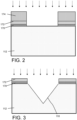
- FIGS. 2-6 show cross-sectional views of a method according to embodiments of the disclosure.
- the method may form IC structure 100 ( FIG. 1 ).
- FIGS. 2 and 3 show forming V-shaped cavity 110 in semiconductor substrate 112.
- any trench isolations (not shown) may be formed to electrically isolate different regions within substrate in a known fashion.
- the forming of V-shaped cavity 110 may include, as shown in FIG. 2 , patterning a nitride layer 170 and a pad oxide layer 172 thereunder using a patterned mask 174 and an etching to remove the layers 170, 172 over substrate 112, e.g., using a reactive ion etch (RIE).
- RIE reactive ion etch
- Mask 174 may include any now known or later developed masking material appropriate for the etching chemistry used. Common masking materials are photoresist (resist) and nitride. Nitride is usually considered to be a "hard mask.” Mask 174 may include a developable organic planarization layer (OPL) on the layer to be etched, a developable anti-reflective coating (ARC) layer on the developable OPL, and a photoresist mask layer on the developable ARC layer. After the etching shown in FIG.
- OPL developable organic planarization layer
- ARC developable anti-reflective coating
- mask 174 may be removed using any known removal process appropriate for the mask material, e.g., a wet etch for hard nitride mask or an ashing process (oxygen dry strip process) for a soft resist-based mask.
- patterned nitride layer 172 may then be used (as a mask) to form V-shaped cavity 110.
- V-shaped cavity 110 may be formed by performing any now known or later developed wet etching process appropriate for semiconductor substrate 112.
- V-shaped cavity 110 may include facets along (111) crystallographic planes of semiconductor substrate 112.
- nitride layer 172 may be removed using any known removal process appropriate for the mask material, e.g., a wet etch for hard nitride mask.
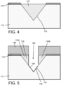
- FIG. 4 shows filling V-shaped cavity 110 with a spacer material 178.
- Spacer material 178 may be deposited using any appropriate deposition technique for the material, such as but not limited to chemical vapor deposition of a nitride.
- Spacer material 178 may include any spacer material such as but not limited to at least one nitride such as silicon nitride and/or other nitride.
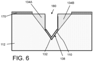
- FIG. 5 shows forming an opening 180 in spacer material 178. Opening 180 creates two spacers 134A-B and exposes a surface 184 of lower portion 138 of V-shaped cavity 110.
- This process may include depositing and patterning a mask 186 and performing an etching such as a reactive ion etch (RIE) to create opening 180.
- RIE reactive ion etch
- Mask 186 may include any now known or later developed masking material appropriate for the etching chemistry used, and as previously described herein. After the etching, mask 186 may be removed using any known removal process appropriate for the mask material, as previously described.
- FIG. 6 shows forming gate dielectric layer 132 on surface 184 ( FIG. 5 ) of lower portion 138 of V-shaped cavity 110.
- Gate dielectric layer 132 may be formed, for example, by thermally growing an oxide on surface 184 of lower portion 138 of V-shaped cavity 110.
- Gate dielectric layer 132 takes the shape of surface 184 of lower portion 138 of V-shaped cavity 110, and has a cross-sectional V-shape between spacers 134A-B.
- FIG. 1 shows forming gate electrode 136 over gate dielectric layer 132 and between spacers 134A-B.
- the process may include depositing gate electrode 136 material, such as polysilicon using any appropriate deposition technique (e.g., CVD), and planarizing.
- the planarizing can include any appropriate planarization technique such as but not limited to chemical mechanical polishing.
- forming gate electrode 136 may include depositing a polysilicon, and planarizing to make upper surface 152 of gate electrode 136 and upper surface 154 of spacers 134A-B coplanar with upper surface 150 of semiconductor substrate 112 (removing pad oxide layer 170 ( FIG. 6 )).
- gate electrode 136 is between spacers 134A-B.
- gate electrode 136, spacers 134A-B and gate dielectric layer 132 are fully within V-shaped cavity 110, as previously described. Again, none of gate structure 130 extends beyond an upper surface 150 of semiconductor substrate 112. As noted, gate electrode 136 has a shape of an irregular pentagon with two parallel sides 160, each side 160 being perpendicular to base 162 (upper surface 152). Spacers 134A-B contact the two parallel sides 160 of gate electrode 136 and a surface of upper portion 139 of V-shaped cavity 110.
- FIG. 1 also shows forming source region 120 and drain region 122 on opposing sides of V-shaped cavity 110.
- Source region 120 and drain region 122 may be formed using any now known or later developed doping process, such as but not limited to ion implantation.
- Metallic interconnects 140 can be formed using any now known or later developed middle-of-line or back-end-of-line processing.
- IC structure 100 provides a smaller gate width, decreased capacitance, increased gain and increased radio frequency (RF) performance compared to planar devices or devices without the gate structure fully within V-shaped cavity.
- RF radio frequency
- the structure and method as described above are used in the fabrication of integrated circuit chips.
- the resulting integrated circuit chips can be distributed by the fabricator in raw wafer form (that is, as a single wafer that has multiple unpackaged chips), as a bare die, or in a packaged form.
- the chip is mounted in a single chip package (such as a plastic carrier, with leads that are affixed to a motherboard or other higher-level carrier) or in a multichip package (such as a ceramic carrier that has either or both surface interconnections or buried interconnections).
- the chip is then integrated with other chips, discrete circuit elements, and/or other signal processing devices as part of either (a) an intermediate product, such as a motherboard, or (b) an end product.
- the end product can be any product that includes integrated circuit chips, ranging from toys and other low-end applications to advanced computer products having a display, a keyboard or other input device, and a central processor.
- Approximating language may be applied to modify any quantitative representation that could permissibly vary without resulting in a change in the basic function to which it is related. Accordingly, a value modified by a term or terms, such as “about”, “approximately” and “substantially”, are not to be limited to the precise value specified. In at least some instances, the approximating language may correspond to the precision of an instrument for measuring the value.
- range limitations may be combined and/or interchanged, such ranges are identified and include all the sub-ranges contained therein unless context or language indicates otherwise. "Approximately” as applied to a particular value of a range applies to both values, and unless otherwise dependent on the precision of the instrument measuring the value, may indicate +/- 5% of the stated value(s).
- An integrated circuit (IC) structure comprising:
- the spacers include at least one nitride and the gate dielectric layer includes an oxide.
- An integrated circuit (IC) structure comprising:
- a method comprising:
- forming the gate electrode includes depositing a polysilicon, and planarizing to make an upper surface of the gate electrode and an upper surface of the spacers coplanar with an upper surface of the semiconductor substrate.
- the gate electrode has substantially vertical sides and a V-shaped bottom surface corresponding to a surface of the gate dielectric layer on a lower portion of the V-shaped cavity, and wherein the spacers contact the substantially vertical sides of the gate electrode and a surface of an upper portion of the V-shaped cavity.
- the gate electrode has a shape of an irregular pentagon with two parallel sides, each side perpendicular to a base, and the spacers contact the two parallel sides of the gate electrode and a surface of an upper portion of the V-shaped cavity.
- the term "width" may be understood as representing a dimension, e.g., a diameter, in a specific direction, e.g., a horizontal direction.
- the gate structure may have a width in a specific direction (e.g., the horizontal direction in FIG. 1 ) such as a dimension measured parallel to an upper surface of the semiconductor substrate 112.
- the direction may be parallel to a direction along which source and drain regions (e.g. source and drain regions 120 and 122 in Fig. 1 ) are separated in the semiconductor substrate.
- horizontal may be understood as representing a direction perpendicular to a normal of a main surface of the semiconductor substrate, where a main surface of the semiconductor substrate may be a surface on or over which a contact such as contact 140 may be disposed.
- substantially may indicate a deviation.
- substantially vertical sides may be understood as reading “vertical sides” in the sense of purely perpendicular to a horizontal direction or deviating from a vertical direction by a tolerable deviation.
- the term "include” and its variants may be interpreted as meaning that an embodiment includes stated features, while not necessarily excluding the presence of other features that are not explicitly stated.
- an integrated circuit (IC) structure comprising:
Landscapes
- Insulated Gate Type Field-Effect Transistor (AREA)
- Engineering & Computer Science (AREA)
- Manufacturing & Machinery (AREA)
- Thin Film Transistor (AREA)
Abstract
An integrated circuit (IC) structure includes a V-shaped cavity in a semiconductor substrate. A source region and a drain region are on opposing sides of the V-shaped cavity. A gate structure includes a gate dielectric layer, spacers, and a gate electrode on the gate dielectric layer between the spacers. The gate structure is fully within the V-shaped cavity. The IC structure provides a switch that finds advantageous application as part of a low noise amplifier. The IC structure provides a smaller gate width, decreased capacitance, increased gain and increased radio frequency (RF) performance compared to planar devices or devices without the gate structure fully within V-shaped cavity.
Description
- The present disclosure relates to integrated circuit (IC) structures and, more particularly, to an IC structure including a switch with a gate electrode fully within a V-shaped cavity.
- IC structures, such as low noise amplifiers, include switches having V-shaped gates that allow for smaller gate width.
- An aspect of the disclosure provides an integrated circuit (IC) structure, comprising: a V-shaped cavity in a semiconductor substrate; a source region and a drain region on opposing sides of the V-shaped cavity; and a gate structure fully within the V-shaped cavity, the gate structure including a gate dielectric layer, spacers, and a gate electrode on the gate dielectric layer between the spacers.
- An aspect of the disclosure provides an integrated circuit (IC) structure, comprising: a V-shaped cavity in a semiconductor substrate; a source region and a drain region on opposing sides of the V-shaped cavity; and a gate structure including a gate dielectric layer, spacers, and a gate electrode on the gate dielectric layer between the spacers, wherein the gate electrode has substantially vertical sides and a V-shaped bottom surface corresponding to a surface of the gate dielectric layer on a lower portion of the V-shaped cavity, and an upper surface of the gate electrode and an upper surface of the spacers are coplanar with an upper surface of the semiconductor substrate.
- An aspect of the disclosure provides a method comprising: forming a V-shaped cavity in a semiconductor substrate; filling the V-shaped cavity with a spacer material; forming an opening in the spacer material, creating two spacers and exposing a surface of a lower portion of the V-shaped cavity; forming a gate dielectric layer on the surface of the lower portion of the V-shaped cavity; forming a gate electrode over the gate dielectric layer and between the spacers, wherein the gate electrode between the spacers, the spacers and the gate dielectric layer are fully within the V-shaped cavity; and forming a source region and a drain region on opposing sides of the V-shaped cavity.
- The embodiments of this disclosure will be described in detail, with reference to the following figures, wherein like designations denote like elements, and wherein:
-
FIG. 1 shows a cross-sectional view of an IC structure, according to embodiments of the disclosure; and -
FIGS. 2-6 show cross-sectional views of a method of forming the IC structure, according to embodiments of the disclosure. - It is noted that the drawings of the disclosure are not necessarily to scale. The drawings are intended to depict only typical aspects of the disclosure, and therefore should not be considered as limiting the scope of the disclosure. In the drawings, like numbering represents like elements between the drawings.
- In the following description, reference is made to the accompanying drawings that form a part thereof, and in which is shown by way of illustration specific illustrative embodiments in which the present teachings may be practiced. These embodiments are described in sufficient detail to enable those skilled in the art to practice the present teachings, and it is to be understood that other embodiments may be used and that changes may be made without departing from the scope of the present teachings. The following description is, therefore, merely illustrative.
- It will be understood that when an element such as a layer, region, or substrate is referred to as being "on" or "over" another element, it may be directly on the other element or intervening elements may also be present. In contrast, when an element is referred to as being "directly on" or "directly over" another element, there may be no intervening elements present. It will also be understood that when an element is referred to as being "connected" or "coupled" to another element, it may be directly connected or coupled to the other element or intervening elements may be present. In contrast, when an element is referred to as being "directly connected" or "directly coupled" to another element, there are no intervening elements present.
- Reference in the specification to "one embodiment" or "an embodiment" of the present disclosure, as well as other variations thereof, means that a particular feature, structure, characteristic, and so forth described in connection with the embodiment is included in at least one embodiment of the present disclosure. Thus, the phrases "in one embodiment" or "in an embodiment," as well as any other variations appearing in various places throughout the specification are not necessarily all referring to the same embodiment. It is to be appreciated that the use of any of the following "/," "and/or," and "at least one of," for example, in the cases of "A/B," "A and/or B" and "at least one of A and B," is intended to encompass the selection of the first listed option (A) only, or the selection of the second listed option (B) only, or the selection of both options (A and B). As a further example, in the cases of "A, B, and/or C" and "at least one of A, B, and C," such phrasing is intended to encompass the first listed option (A) only, or the selection of the second listed option (B) only, or the selection of the third listed option (C) only, or the selection of the first and the second listed options (A and B), or the selection of the first and third listed options (A and C) only, or the selection of the second and third listed options (B and C) only, or the selection of all three options (A and B and C). This may be extended, as readily apparent by one of ordinary skill in the art, for as many items listed.
- Embodiments of the disclosure provide an integrated circuit (IC) structure including a V-shaped cavity in a semiconductor substrate. A source region and a drain region are on opposing sides of the V-shaped cavity. A gate structure includes a gate dielectric layer, spacers, and a gate electrode on the gate dielectric layer between the spacers. The gate structure is fully within the V-shaped cavity. The IC structure provides a switch that finds advantageous application as part of a low noise amplifier. The IC structure provides a smaller gate width, decreased capacitance, increased gain and increased radio frequency (RF) performance compared to planar devices or devices without the gate structure fully within V-shaped cavity.
-
FIG. 1 shows a cross-sectional view of an IC structure 100 according to embodiments of the disclosure. IC structure 100 includes a switch 102 that, as will be described, may be configured as a low noise amplifier (LNA), e.g., as part of an LNA application. IC structure includes a V-shaped cavity 110 in asemiconductor substrate 112.Semiconductor substrate 112 typically includes a wafer of semiconductor material such as silicon, germanium, silicon germanium, or silicon carbide. Asubstrate 112 may also comprise an organic semiconductor or a layered semiconductor such as, for example, Si/SiGe, a silicon-on-insulator or a SiGe-on-insulator. A portion orentire semiconductor substrate 112 may be amorphous, polycrystalline, or monocrystalline. In this example,semiconductor substrate 112 may include bulk semiconductor, but other forms of substrate may also be possible.Semiconductor substrate 112 may optionally include any desired dopant to customize the electrical properties thereof for the type of switch 102, e.g., PFET or NFET, to be provided by IC structure 100. V-shaped cavity 110 may include facets along (111) crystallographic planes ofsemiconductor substrate 112. - IC structure 100 also includes a
source region 120 and adrain region 122 on opposing sides of V-shaped cavity 110. Source anddrain regions additional doping regions 124 insemiconductor substrate 112 underneathspacers 134A-B (described herein) andsource region 120 anddrain region 122.Doped regions 124 may include any now known or later developed regions of additional dopant(s) to provide desired electrical properties for IC structure 100 such as but not limited to doped wells (example shown by dashed lines), halos, or extensions. - IC structure 100 also includes a
gate structure 130 fully within V-shaped cavity 110.Gate structure 130 includes a gatedielectric layer 132,spacers gate electrode 136 on gatedielectric layer 132 betweenspacers Gate electrode 136 may include any now known or later developed polyconductor, e.g., polysilicon or metal gate material. Gatedielectric layer 132 has a different material composition thanspacers 134A-B, e.g., with different dielectric constants. In one example,spacers 134A-B include at least one nitride such as silicon nitride and/or other nitrides, and gatedielectric layer 132 includes an oxide such as silicon oxide. Gatedielectric layer 132 contacts a surface of alower portion 138 of V-shaped cavity 110 and is betweenspacers 134A-B. Spacers 134A-B contact a surface of anupper portion 139 of V-shaped cavity 110. - IC structure 100 may also include any variety of
metallic interconnect 140 ongate electrode 136,source region 120 and/ordrain region 122.Metallic interconnects 140 may include any now known or later developed metal wire or contact formed in an inter-layer dielectric (ILD) layer (not shown) oversubstrate 112. - In contrast to conventional recessed gate devices,
gate structure 130 is fully within V-shaped cavity 110, i.e., none ofgate structure 130 extends beyond anupper surface 150 ofsemiconductor substrate 112. More particularly, an upper surface 152 ofgate electrode 136 and anupper surface 154 ofspacers 134A-B are coplanar withupper surface 150 ofsemiconductor substrate 112. However,gate electrode 136 does not fully fill V-shape cavity 110. Rather,gate electrode 136 has a shape of an irregular pentagon with twoparallel sides 160, eachside 160 perpendicular to a base 162, i.e., same side as upper surface 152.Spacers 134A-B contact the twoparallel sides 160 ofgate electrode 136 and a surface ofupper portion 139 of V-shaped cavity 110.Gate electrode 136 may also be stated to have a shape of a rectangle with a coincident isosceles triangle placed on one side, or an isosceles right pentagon. In this regard,gate electrode 136 has substantiallyvertical sides 160 and a V-shaped bottom surface 164 corresponding to an upper surface of gatedielectric layer 132 onlower portion 138 of V-shaped cavity 110. As used herein, "substantially vertical" indicates with approximately +/- 10° of vertical.Spacers 134A-B contact the substantiallyvertical sides 160 ofgate electrode 136 and a surface ofupper portion 139 of V-shaped cavity 110. As observed inFIG. 1 , gatedielectric layer 132,gate electrode 136 andspacers 134A-B fully fill V-shaped cavity 110. -
FIGS. 2-6 show cross-sectional views of a method according to embodiments of the disclosure. The method may form IC structure 100 (FIG. 1 ).FIGS. 2 and 3 show forming V-shapedcavity 110 insemiconductor substrate 112. At this stage, any trench isolations (not shown) may be formed to electrically isolate different regions within substrate in a known fashion. The forming of V-shapedcavity 110 may include, as shown inFIG. 2 , patterning anitride layer 170 and apad oxide layer 172 thereunder using a patternedmask 174 and an etching to remove thelayers substrate 112, e.g., using a reactive ion etch (RIE).Mask 174 may include any now known or later developed masking material appropriate for the etching chemistry used. Common masking materials are photoresist (resist) and nitride. Nitride is usually considered to be a "hard mask."Mask 174 may include a developable organic planarization layer (OPL) on the layer to be etched, a developable anti-reflective coating (ARC) layer on the developable OPL, and a photoresist mask layer on the developable ARC layer. After the etching shown inFIG. 2 ,mask 174 may be removed using any known removal process appropriate for the mask material, e.g., a wet etch for hard nitride mask or an ashing process (oxygen dry strip process) for a soft resist-based mask. As shown inFIG. 3 , patternednitride layer 172 may then be used (as a mask) to form V-shapedcavity 110. V-shapedcavity 110 may be formed by performing any now known or later developed wet etching process appropriate forsemiconductor substrate 112. As noted, V-shapedcavity 110 may include facets along (111) crystallographic planes ofsemiconductor substrate 112. After the etching shown inFIG. 3 ,nitride layer 172 may be removed using any known removal process appropriate for the mask material, e.g., a wet etch for hard nitride mask. -
FIG. 4 shows filling V-shapedcavity 110 with aspacer material 178.Spacer material 178 may be deposited using any appropriate deposition technique for the material, such as but not limited to chemical vapor deposition of a nitride.Spacer material 178 may include any spacer material such as but not limited to at least one nitride such as silicon nitride and/or other nitride. -
FIG. 5 shows forming anopening 180 inspacer material 178.Opening 180 creates twospacers 134A-B and exposes asurface 184 oflower portion 138 of V-shapedcavity 110. This process may include depositing and patterning amask 186 and performing an etching such as a reactive ion etch (RIE) to createopening 180.Mask 186 may include any now known or later developed masking material appropriate for the etching chemistry used, and as previously described herein. After the etching,mask 186 may be removed using any known removal process appropriate for the mask material, as previously described. -
FIG. 6 shows forminggate dielectric layer 132 on surface 184 (FIG. 5 ) oflower portion 138 of V-shapedcavity 110.Gate dielectric layer 132 may be formed, for example, by thermally growing an oxide onsurface 184 oflower portion 138 of V-shapedcavity 110.Gate dielectric layer 132 takes the shape ofsurface 184 oflower portion 138 of V-shapedcavity 110, and has a cross-sectional V-shape betweenspacers 134A-B. -
FIG. 1 shows forminggate electrode 136 overgate dielectric layer 132 and betweenspacers 134A-B. The process may include depositinggate electrode 136 material, such as polysilicon using any appropriate deposition technique (e.g., CVD), and planarizing. The planarizing can include any appropriate planarization technique such as but not limited to chemical mechanical polishing. More particularly, forminggate electrode 136 may include depositing a polysilicon, and planarizing to make upper surface 152 ofgate electrode 136 andupper surface 154 ofspacers 134A-B coplanar withupper surface 150 of semiconductor substrate 112 (removing pad oxide layer 170 (FIG. 6 )). As noted,gate electrode 136 is betweenspacers 134A-B. Further,gate electrode 136,spacers 134A-B andgate dielectric layer 132 are fully within V-shapedcavity 110, as previously described. Again, none ofgate structure 130 extends beyond anupper surface 150 ofsemiconductor substrate 112. As noted,gate electrode 136 has a shape of an irregular pentagon with twoparallel sides 160, eachside 160 being perpendicular to base 162 (upper surface 152).Spacers 134A-B contact the twoparallel sides 160 ofgate electrode 136 and a surface ofupper portion 139 of V-shapedcavity 110. -
FIG. 1 also shows formingsource region 120 and drainregion 122 on opposing sides of V-shapedcavity 110.Source region 120 and drainregion 122 may be formed using any now known or later developed doping process, such as but not limited to ion implantation.Metallic interconnects 140 can be formed using any now known or later developed middle-of-line or back-end-of-line processing. - Embodiments of the disclosure provide various technical and commercial advantages, examples of which are discussed herein. IC structure 100 provides a smaller gate width, decreased capacitance, increased gain and increased radio frequency (RF) performance compared to planar devices or devices without the gate structure fully within V-shaped cavity.
- The structure and method as described above are used in the fabrication of integrated circuit chips. The resulting integrated circuit chips can be distributed by the fabricator in raw wafer form (that is, as a single wafer that has multiple unpackaged chips), as a bare die, or in a packaged form. In the latter case the chip is mounted in a single chip package (such as a plastic carrier, with leads that are affixed to a motherboard or other higher-level carrier) or in a multichip package (such as a ceramic carrier that has either or both surface interconnections or buried interconnections). In any case the chip is then integrated with other chips, discrete circuit elements, and/or other signal processing devices as part of either (a) an intermediate product, such as a motherboard, or (b) an end product. The end product can be any product that includes integrated circuit chips, ranging from toys and other low-end applications to advanced computer products having a display, a keyboard or other input device, and a central processor.
- The terminology used herein is for the purpose of describing particular embodiments only and is not intended to be limiting of the disclosure. As used herein, the singular forms "a", "an" and "the" are intended to include the plural forms as well, unless the context clearly indicates otherwise. It will be further understood that the terms "comprises" and/or "comprising," when used in this specification, specify the presence of stated features, integers, steps, operations, elements, and/or components, but do not preclude the presence or addition of one or more other features, integers, steps, operations, elements, components, and/or groups thereof. "Optional" or "optionally" means that the subsequently described event or circumstance may or may not occur, and that the description includes instances where the event occurs and instances where it does not.
- Approximating language, as used herein throughout the specification and claims, may be applied to modify any quantitative representation that could permissibly vary without resulting in a change in the basic function to which it is related. Accordingly, a value modified by a term or terms, such as "about", "approximately" and "substantially", are not to be limited to the precise value specified. In at least some instances, the approximating language may correspond to the precision of an instrument for measuring the value. Here and throughout the specification and claims, range limitations may be combined and/or interchanged, such ranges are identified and include all the sub-ranges contained therein unless context or language indicates otherwise. "Approximately" as applied to a particular value of a range applies to both values, and unless otherwise dependent on the precision of the instrument measuring the value, may indicate +/- 5% of the stated value(s).
- The corresponding structures, materials, acts, and equivalents of all means or step plus function elements in the claims below are intended to include any structure, material, or act for performing the function in combination with other claimed elements as specifically claimed. The description of the present disclosure has been presented for purposes of illustration and description, but is not intended to be exhaustive or limited to the disclosure in the form disclosed. Many modifications and variations will be apparent to those of ordinary skill in the art without departing from the scope and spirit of the disclosure. The embodiment was chosen and described in order to best explain the principles of the disclosure and the practical application, and to enable others of ordinary skill in the art to understand the disclosure for various embodiments with various modifications as are suited to the particular use contemplated.
- In summary, the following embodiments are explicitly disclosed.
- An integrated circuit (IC) structure, comprising:
- a V-shaped cavity in a semiconductor substrate;
- a source region and a drain region on opposing sides of the V-shaped cavity; and
- a gate structure, the gate structure including a gate dielectric layer, spacers, and a gate electrode on the gate dielectric layer between the spacers. In examples herein, the gate structure may be fully within the V-shaped cavity.
- The IC structure of embodiment 1, wherein an upper surface of the gate structure and an upper surface of the spacers are coplanar with an upper surface of the semiconductor substrate.
- The IC structure of
embodiment 1 or 2, wherein the gate electrode has substantially vertical sides and a V-shaped bottom surface corresponding to a surface of the gate dielectric layer on a lower portion of the V-shaped cavity. - The IC structure of
embodiment 3, wherein the spacers contact the substantially vertical sides of the gate electrode and a surface of an upper portion of the V-shaped cavity. - The IC structure of one of embodiments 1 to 4, wherein the gate electrode has a shape of an irregular pentagon with two parallel sides, each side perpendicular to a base.
- The IC structure of embodiment 5, wherein the spacers contact the two parallel sides of the gate electrode and a surface of an upper portion of the V-shaped cavity.
- The IC structure of one of embodiments 1 to 6, wherein the gate dielectric layer has a different material composition than the spacers.
- The IC structure of
embodiment 7, wherein the spacers include at least one nitride and the gate dielectric layer includes an oxide. - The IC structure of one of embodiments 1 to 8, wherein the V-shaped cavity includes facets along (111) crystallographic planes of the semiconductor substrate.
- The IC structure of one of embodiments 1 to 9, further comprising doping regions in the semiconductor substrate underneath the spacers and the source region and the drain region.
- The IC structure of one of embodiments 1 to 10, further comprising a metallic interconnect on the gate electrode.
- The IC structure of one of embodiments 1 to 11, wherein the IC structure is configured as a low noise amplifier.
- The IC structure of one of embodiments 1 to 12, wherein the gate electrode has substantially vertical sides and a V-shaped bottom surface corresponding to a surface of the gate dielectric layer on a lower portion of the V-shaped cavity, and an upper surface of the gate electrode and an upper surface of the spacers are coplanar with an upper surface of the semiconductor substrate.
- An integrated circuit (IC) structure, comprising:
- a V-shaped cavity in a semiconductor substrate;
- a source region and a drain region on opposing sides of the V-shaped cavity; and
- a gate structure including a gate dielectric layer, spacers, and a gate electrode on the gate dielectric layer between the spacers,
- wherein the gate electrode has substantially vertical sides and a V-shaped bottom surface corresponding to a surface of the gate dielectric layer on a lower portion of the V-shaped cavity, and an upper surface of the gate electrode and an upper surface of the spacers are coplanar with an upper surface of the semiconductor substrate.
- The IC structure of
embodiment 13 or 14, wherein the spacers contact the substantially vertical sides of the gate electrode and a surface of an upper portion of the V-shaped cavity. - The IC structure of one of
embodiments 13 to 15, wherein the gate electrode has a shape of an irregular pentagon with two parallel sides, each side perpendicular to a base, and wherein the spacers contact the two parallel sides of the gate electrode and a surface of an upper portion of the V-shaped cavity. - A method comprising:
- forming a V-shaped cavity in a semiconductor substrate;
- filling the V-shaped cavity with a spacer material;
- forming an opening in the spacer material, creating two spacers and exposing a surface of a lower portion of the V-shaped cavity;
- forming a gate dielectric layer on the surface of the lower portion of the V-shaped cavity;
- forming a gate electrode over the gate dielectric layer and between the spacers, wherein the gate electrode between the spacers, the spacers and the gate dielectric layer are fully within the V-shaped cavity; and
- forming a source region and a drain region on opposing sides of the V-shaped cavity.
- The method of embodiment 17, wherein the gate electrode, the spacers and the gate dielectric layer are fully within the V-shaped cavity.
- The method of embodiment 17 or 18, wherein forming the gate electrode includes depositing a polysilicon, and planarizing to make an upper surface of the gate electrode and an upper surface of the spacers coplanar with an upper surface of the semiconductor substrate.
- The method of one of embodiments 17 to 19, wherein the gate electrode has substantially vertical sides and a V-shaped bottom surface corresponding to a surface of the gate dielectric layer on a lower portion of the V-shaped cavity, and wherein the spacers contact the substantially vertical sides of the gate electrode and a surface of an upper portion of the V-shaped cavity.
- The method of one of embodiments 17 to 20, wherein the gate electrode has a shape of an irregular pentagon with two parallel sides, each side perpendicular to a base, and the spacers contact the two parallel sides of the gate electrode and a surface of an upper portion of the V-shaped cavity.
- The method of one of embodiments 17 to 21, wherein the IC structure of one of embodiments 1 to 16 is formed.
- At least in the embodiments above, the term "width" may be understood as representing a dimension, e.g., a diameter, in a specific direction, e.g., a horizontal direction. For example, the gate structure may have a width in a specific direction (e.g., the horizontal direction in
FIG. 1 ) such as a dimension measured parallel to an upper surface of thesemiconductor substrate 112. For example, the direction may be parallel to a direction along which source and drain regions (e.g. source and drainregions Fig. 1 ) are separated in the semiconductor substrate. Herein, horizontal may be understood as representing a direction perpendicular to a normal of a main surface of the semiconductor substrate, where a main surface of the semiconductor substrate may be a surface on or over which a contact such ascontact 140 may be disposed. - The term "substantially" may indicate a deviation. For example, "substantially vertical sides" may be understood as reading "vertical sides" in the sense of purely perpendicular to a horizontal direction or deviating from a vertical direction by a tolerable deviation.
- At least in the embodiments above, the term "include" and its variants may be interpreted as meaning that an embodiment includes stated features, while not necessarily excluding the presence of other features that are not explicitly stated.
- In explicit examples of the embodiments above, embodiment 1 above may be read as follows: An integrated circuit (IC) structure, comprising:
- a V-shaped cavity in a semiconductor substrate;
- a source region and a drain region on opposing sides of the V-shaped cavity; and
- a gate structure fully within the V-shaped cavity, the gate structure including a gate dielectric layer, spacers, and a gate electrode on the gate dielectric layer between the spacers.
Claims (15)
- An integrated circuit (IC) structure, comprising:a V-shaped cavity in a semiconductor substrate;a source region and a drain region on opposing sides of the V-shaped cavity; anda gate structure, preferably fully within the V-shaped cavity, the gate structure including a gate dielectric layer, spacers, and a gate electrode on the gate dielectric layer between the spacers.
- The IC structure of claim 1, wherein an upper surface of the gate structure and an upper surface of the spacers are coplanar with an upper surface of the semiconductor substrate.
- The IC structure of claim 1 or 2, wherein the gate electrode has substantially vertical sides and a V-shaped bottom surface corresponding to a surface of the gate dielectric layer on a lower portion of the V-shaped cavity, the spacers preferably contacting the substantially vertical sides of the gate electrode and a surface of an upper portion of the V-shaped cavity.
- The IC structure of one of claims 1 to 3, wherein the gate electrode has a shape of an irregular pentagon with two parallel sides, each side perpendicular to a base, the spacers preferably contacting the two parallel sides of the gate electrode and a surface of an upper portion of the V-shaped cavity.
- The IC structure of one of claims 1 to 4, wherein the gate dielectric layer has a different material composition than the spacers, the spacers preferably including at least one nitride and the gate dielectric layer includes an oxide.
- The IC structure of one of claims 1 to 5, wherein the V-shaped cavity includes facets along (111) crystallographic planes of the semiconductor substrate.
- The IC structure of one of claims 1 to 6, further comprising doping regions in the semiconductor substrate underneath the spacers and the source region and the drain region.
- The IC structure of one of claims 1 to 7, further comprising a metallic interconnect on the gate electrode.
- The IC structure of one of claims 1 to 8, wherein the IC structure is configured as a low noise amplifier.
- A method comprising:forming a V-shaped cavity in a semiconductor substrate;filling the V-shaped cavity with a spacer material;forming an opening in the spacer material, creating two spacers and exposing a surface of a lower portion of the V-shaped cavity;forming a gate dielectric layer on the surface of the lower portion of the V-shaped cavity;forming a gate electrode over the gate dielectric layer and between the spacers, wherein the gate electrode between the spacers, the spacers and the gate dielectric layer are fully within the V-shaped cavity; andforming a source region and a drain region on opposing sides of the V-shaped cavity.
- The method of claim 10, wherein the gate electrode, the spacers and the gate dielectric layer are fully within the V-shaped cavity.
- The method of claim 10 or 11, wherein forming the gate electrode includes depositing a polysilicon, and planarizing to make an upper surface of the gate electrode and an upper surface of the spacers coplanar with an upper surface of the semiconductor substrate.
- The method of one of claims 10 to 12, wherein the gate electrode has substantially vertical sides and a V-shaped bottom surface corresponding to a surface of the gate dielectric layer on a lower portion of the V-shaped cavity, and wherein the spacers contact the substantially vertical sides of the gate electrode and a surface of an upper portion of the V-shaped cavity.
- The method of one of claims 10 to 13, wherein the gate electrode has a shape of an irregular pentagon with two parallel sides, each side perpendicular to a base, and the spacers contact the two parallel sides of the gate electrode and a surface of an upper portion of the V-shaped cavity.
- The method of one of claims 10 to 14, wherein the IC structure of one of claims 1 to 9 is formed.
Applications Claiming Priority (1)
| Application Number | Priority Date | Filing Date | Title |
|---|---|---|---|
| US18/059,186 US12610605B2 (en) | 2022-11-28 | 2022-11-28 | IC structure with gate electrode fully within V-shaped cavity |
Publications (1)
| Publication Number | Publication Date |
|---|---|
| EP4376092A1 true EP4376092A1 (en) | 2024-05-29 |
Family
ID=88291069
Family Applications (1)
| Application Number | Title | Priority Date | Filing Date |
|---|---|---|---|
| EP23201745.9A Pending EP4376092A1 (en) | 2022-11-28 | 2023-10-05 | Ic structure with gate electrode fully within v-shaped cavity |
Country Status (3)
| Country | Link |
|---|---|
| US (1) | US12610605B2 (en) |
| EP (1) | EP4376092A1 (en) |
| CN (1) | CN118099195A (en) |
Citations (3)
| Publication number | Priority date | Publication date | Assignee | Title |
|---|---|---|---|---|
| US20010045597A1 (en) * | 1998-06-25 | 2001-11-29 | Kazumi Nishinohara | Mis semiconductor device and method of fabricating the same |
| US20110008940A1 (en) * | 2008-08-26 | 2011-01-13 | Taiwan Semiconductor Manufacturing Co., Ltd. | Self-aligned v-channel mosfet |
| US20150295066A1 (en) * | 2012-09-05 | 2015-10-15 | Commissariat A L'energie Atomique Et Aux Ene Alt | Process for producing fet transistors |
Family Cites Families (82)
| Publication number | Priority date | Publication date | Assignee | Title |
|---|---|---|---|---|
| US3975752A (en) * | 1973-04-04 | 1976-08-17 | Harris Corporation | Junction field effect transistor |
| US3892608A (en) * | 1974-02-28 | 1975-07-01 | Motorola Inc | Method for filling grooves and moats used on semiconductor devices |
| JPS5928992B2 (en) * | 1975-02-14 | 1984-07-17 | 日本電信電話株式会社 | MOS transistor and its manufacturing method |
| US4037306A (en) * | 1975-10-02 | 1977-07-26 | Motorola, Inc. | Integrated circuit and method |
| US4003036A (en) * | 1975-10-23 | 1977-01-11 | American Micro-Systems, Inc. | Single IGFET memory cell with buried storage element |
| US4048649A (en) * | 1976-02-06 | 1977-09-13 | Transitron Electronic Corporation | Superintegrated v-groove isolated bipolar and vmos transistors |
| DE2619713C2 (en) * | 1976-05-04 | 1984-12-20 | Siemens AG, 1000 Berlin und 8000 München | Semiconductor memory |
| US4084175A (en) | 1976-09-30 | 1978-04-11 | Research Corporation | Double implanted planar mos device with v-groove and process of manufacture thereof |
| US4119996A (en) * | 1977-07-20 | 1978-10-10 | The United States Of America As Represented By The Administrator Of The National Aeronautics And Space Administration | Complementary DMOS-VMOS integrated circuit structure |
| DE2737073C3 (en) * | 1977-08-17 | 1981-09-17 | Siemens AG, 1000 Berlin und 8000 München | Method for producing an insulated gate field effect transistor for a single transistor memory cell |
| US4116720A (en) * | 1977-12-27 | 1978-09-26 | Burroughs Corporation | Method of making a V-MOS field effect transistor for a dynamic memory cell having improved capacitance |
| JPS54154977A (en) * | 1978-05-29 | 1979-12-06 | Fujitsu Ltd | Semiconductor device and its manufacture |
| US4338620A (en) * | 1978-08-31 | 1982-07-06 | Fujitsu Limited | Semiconductor devices having improved alignment marks |
| JPS5537250U (en) * | 1978-08-31 | 1980-03-10 | ||
| US4231056A (en) * | 1978-10-20 | 1980-10-28 | Harris Corporation | Moat resistor ram cell |
| US4269636A (en) * | 1978-12-29 | 1981-05-26 | Harris Corporation | Method of fabricating self-aligned bipolar transistor process and device utilizing etching and self-aligned masking |
| US4225879A (en) * | 1979-01-26 | 1980-09-30 | Burroughs Corporation | V-MOS Field effect transistor for a dynamic memory cell having improved capacitance |
| US4272302A (en) * | 1979-09-05 | 1981-06-09 | The United States Of America As Represented By The Administrator Of The National Aeronautics And Space Administration | Method of making V-MOS field effect transistors utilizing a two-step anisotropic etching and ion implantation |
| US4268537A (en) * | 1979-12-03 | 1981-05-19 | Rca Corporation | Method for manufacturing a self-aligned contact in a grooved semiconductor surface |
| US4295924A (en) * | 1979-12-17 | 1981-10-20 | International Business Machines Corporation | Method for providing self-aligned conductor in a V-groove device |
| US4364074A (en) * | 1980-06-12 | 1982-12-14 | International Business Machines Corporation | V-MOS Device with self-aligned multiple electrodes |
| DE3129558A1 (en) * | 1980-07-28 | 1982-03-18 | Tokyo Shibaura Denki K.K., Kawasaki, Kanagawa | METHOD FOR PRODUCING AN INTEGRATED SEMICONDUCTOR CIRCUIT |
| US4326332A (en) * | 1980-07-28 | 1982-04-27 | International Business Machines Corp. | Method of making a high density V-MOS memory array |
| US4409609A (en) * | 1981-03-18 | 1983-10-11 | Fujitsu Limited | Semiconductor device and method of manufacturing the same |
| FR2513016A1 (en) * | 1981-09-14 | 1983-03-18 | Radiotechnique Compelec | HIGH VOLTAGE TRANSFORMER V MOS AND METHOD FOR MANUFACTURING THE SAME |
| JPS58106870A (en) * | 1981-12-18 | 1983-06-25 | Nissan Motor Co Ltd | Power metal oxide semiconductor field-effect transistor |
| US4468414A (en) * | 1983-07-29 | 1984-08-28 | Harris Corporation | Dielectric isolation fabrication for laser trimming |
| JPS6161441A (en) * | 1984-09-03 | 1986-03-29 | Toshiba Corp | Manufacture of semiconductor device |
| US4859621A (en) * | 1988-02-01 | 1989-08-22 | General Instrument Corp. | Method for setting the threshold voltage of a vertical power MOSFET |
| US5362973A (en) * | 1990-06-25 | 1994-11-08 | Xerox Corporation | Quantum fabricated via photo induced evaporation enhancement during in situ epitaxial growth |
| KR940010564B1 (en) * | 1991-10-10 | 1994-10-24 | 금성일렉트론 주식회사 | Field effect transistor and its manufacturing method |
| US5395777A (en) * | 1994-04-06 | 1995-03-07 | United Microelectronics Corp. | Method of producing VDMOS transistors |
| US5466616A (en) * | 1994-04-06 | 1995-11-14 | United Microelectronics Corp. | Method of producing an LDMOS transistor having reduced dimensions, reduced leakage, and a reduced propensity to latch-up |
| US5600168A (en) * | 1994-04-20 | 1997-02-04 | Lg Semicon Co., Ltd. | Semiconductor element and method for fabricating the same |
| JPH0822998A (en) * | 1994-07-06 | 1996-01-23 | Mitsubishi Electric Corp | Semiconductor device and manufacturing method thereof |
| JPH0878533A (en) * | 1994-08-31 | 1996-03-22 | Nec Corp | Semiconductor device and manufacturing method thereof |
| JP3239202B2 (en) * | 1995-12-01 | 2001-12-17 | シャープ株式会社 | MOS transistor and method of manufacturing the same |
| JP3320641B2 (en) * | 1996-09-13 | 2002-09-03 | 株式会社東芝 | Memory cell |
| US5808340A (en) | 1996-09-18 | 1998-09-15 | Advanced Micro Devices, Inc. | Short channel self aligned VMOS field effect transistor |
| WO1998012741A1 (en) * | 1996-09-18 | 1998-03-26 | Advanced Micro Devices, Inc. | Short channel non-self aligned vmos field effect transistor |
| TW327241B (en) * | 1997-07-24 | 1998-02-21 | United Semiconductor Corp | The method for lowing down gate boundary capacitor |
| TW392357B (en) * | 1998-02-10 | 2000-06-01 | United Microelectronics Corp | Manufacturing method for semiconductor device and structure manufactured by the same |
| US6078078A (en) * | 1998-10-01 | 2000-06-20 | Advanced Micro Devices, Inc. | V-gate transistor |
| US6018179A (en) * | 1998-11-05 | 2000-01-25 | Advanced Micro Devices | Transistors having a scaled channel length and integrated spacers with enhanced silicidation properties |
| US6380027B2 (en) * | 1999-01-04 | 2002-04-30 | International Business Machines Corporation | Dual tox trench dram structures and process using V-groove |
| JP2000332242A (en) * | 1999-05-21 | 2000-11-30 | Mitsubishi Electric Corp | Semiconductor device and manufacturing method thereof |
| US6433371B1 (en) * | 2000-01-29 | 2002-08-13 | Advanced Micro Devices, Inc. | Controlled gate length and gate profile semiconductor device |
| GB2362755A (en) * | 2000-05-25 | 2001-11-28 | Nanogate Ltd | Thin film field effect transistor with a conical structure |
| US6445035B1 (en) * | 2000-07-24 | 2002-09-03 | Fairchild Semiconductor Corporation | Power MOS device with buried gate and groove |
| JP2004111611A (en) * | 2002-09-18 | 2004-04-08 | Renesas Technology Corp | Semiconductor device and method of manufacturing the same |
| JP4320167B2 (en) * | 2002-12-12 | 2009-08-26 | 忠弘 大見 | Semiconductor device and method for manufacturing silicon oxynitride film |
| US7795094B2 (en) * | 2004-09-02 | 2010-09-14 | Micron Technology, Inc. | Recessed gate dielectric antifuse |
| US7217968B2 (en) * | 2004-12-15 | 2007-05-15 | International Business Machines Corporation | Recessed gate for an image sensor |
| KR100771539B1 (en) | 2005-12-29 | 2007-10-31 | 주식회사 하이닉스반도체 | Semiconductor device having recess gate and manufacturing method thereof |
| US7456450B2 (en) * | 2006-02-09 | 2008-11-25 | International Business Machines Corporation | CMOS devices with hybrid channel orientations and method for fabricating the same |
| JP5034278B2 (en) * | 2006-03-10 | 2012-09-26 | 日産自動車株式会社 | Manufacturing method of semiconductor device |
| US7557002B2 (en) * | 2006-08-18 | 2009-07-07 | Micron Technology, Inc. | Methods of forming transistor devices |
| US7528027B1 (en) * | 2008-03-25 | 2009-05-05 | International Business Machines Corporation | Structure and method for manufacturing device with ultra thin SOI at the tip of a V-shape channel |
| US20090242941A1 (en) * | 2008-03-25 | 2009-10-01 | International Business Machines Corporation | Structure and method for manufacturing device with a v-shape channel nmosfet |
| TWI509774B (en) * | 2009-05-19 | 2015-11-21 | 村田製作所股份有限公司 | A semiconductor switching device, and a method of manufacturing a semiconductor switching device |
| US8076735B2 (en) * | 2009-10-02 | 2011-12-13 | United Microelectronics Corp. | Semiconductor device with trench of various widths |
| US9048254B2 (en) * | 2009-12-02 | 2015-06-02 | United Microelectronics Corp. | Semiconductor structure having a metal gate with side wall spacers |
| JP5510309B2 (en) * | 2010-12-22 | 2014-06-04 | 株式会社デンソー | Silicon carbide semiconductor device and manufacturing method thereof |
| US8603868B2 (en) * | 2011-12-19 | 2013-12-10 | International Business Machines Corporation | V-groove source/drain MOSFET and process for fabricating same |
| US10164082B2 (en) * | 2012-05-04 | 2018-12-25 | Stc.Unm | Growth of cubic crystalline phase structure on silicon substrates and devices comprising the cubic crystalline phase structure |
| US8896032B2 (en) * | 2013-01-23 | 2014-11-25 | International Business Machines Corporation | Self-aligned biosensors with enhanced sensitivity |
| US9893183B2 (en) | 2014-07-10 | 2018-02-13 | Taiwan Semiconductor Manufacturing Company Ltd. | Semiconductor structure and manufacturing method thereof |
| KR102192571B1 (en) * | 2014-12-04 | 2020-12-17 | 삼성전자주식회사 | Semiconductor device having buffer layer and method of forming the same |
| CN107275210B (en) * | 2016-04-06 | 2023-05-02 | 联华电子股份有限公司 | Semiconductor element and manufacturing method thereof |
| EP3474316B1 (en) * | 2016-07-25 | 2021-03-03 | Mitsubishi Electric Corporation | Semiconductor device |
| US11189693B2 (en) * | 2019-05-02 | 2021-11-30 | International Business Machines Corporation | Transistor having reduced contact resistance |
| US11348957B2 (en) * | 2019-12-27 | 2022-05-31 | Omnivision Technologies, Inc. | Transistor having increased effective channel width |
| DE112021002411T5 (en) * | 2020-04-17 | 2023-02-16 | Mitsubishi Electric Corporation | Power semiconductor device, method of manufacturing a power semiconductor device, and power conversion device |
| US12125891B2 (en) * | 2020-07-22 | 2024-10-22 | Taiwan Semiconductor Manufacturing Co., Ltd. | Semiconductor device having gate spacers extending below a fin top surface |
| US11810940B2 (en) * | 2020-10-26 | 2023-11-07 | Omnivision Technologies, Inc. | Pointed-trench pixel-array substrate and associated fabrication method |
| US11621336B2 (en) * | 2021-05-20 | 2023-04-04 | Omnivision Technologies, Inc. | Pyramid-shaped transistors |
| TWI907478B (en) * | 2021-08-09 | 2025-12-11 | 聯華電子股份有限公司 | Semiconductor memory device and fabrication method thereof |
| CN116314324B (en) * | 2021-12-20 | 2026-05-01 | 联华电子股份有限公司 | Semiconductor device and method for manufacturing the same |
| US11650381B1 (en) * | 2022-02-12 | 2023-05-16 | Globalfoundries U.S. Inc. | PIC die and package with cover for multiple level and multiple depth connections of fibers to on-chip optical components |
| US12557364B2 (en) * | 2022-10-28 | 2026-02-17 | Taiwan Semiconductor Manufacturing Company, Ltd. | Semiconductor device with gate isolation structure |
| US20250056866A1 (en) * | 2023-08-10 | 2025-02-13 | Taiwan Semiconductor Manufacturing Co., Ltd. | Semiconductor device |
| KR20250073948A (en) * | 2023-11-20 | 2025-05-27 | 삼성전자주식회사 | Semiconductor device |
-
2022
- 2022-11-28 US US18/059,186 patent/US12610605B2/en active Active
-
2023
- 2023-10-05 EP EP23201745.9A patent/EP4376092A1/en active Pending
- 2023-10-25 CN CN202311390839.6A patent/CN118099195A/en active Pending
Patent Citations (3)
| Publication number | Priority date | Publication date | Assignee | Title |
|---|---|---|---|---|
| US20010045597A1 (en) * | 1998-06-25 | 2001-11-29 | Kazumi Nishinohara | Mis semiconductor device and method of fabricating the same |
| US20110008940A1 (en) * | 2008-08-26 | 2011-01-13 | Taiwan Semiconductor Manufacturing Co., Ltd. | Self-aligned v-channel mosfet |
| US20150295066A1 (en) * | 2012-09-05 | 2015-10-15 | Commissariat A L'energie Atomique Et Aux Ene Alt | Process for producing fet transistors |
Also Published As
| Publication number | Publication date |
|---|---|
| US20240178290A1 (en) | 2024-05-30 |
| US12610605B2 (en) | 2026-04-21 |
| CN118099195A (en) | 2024-05-28 |
Similar Documents
| Publication | Publication Date | Title |
|---|---|---|
| CN109244033B (en) | RF switch with air gap structure | |
| US10916468B2 (en) | Semiconductor device with buried local interconnects | |
| US10411107B2 (en) | Semiconductor device with airgap spacer for transistor and related method | |
| US20190081138A1 (en) | Switch with local silicon on insulator (soi) and deep trench isolation | |
| US11728348B2 (en) | Vertically stacked field effect transistors | |
| US10756184B2 (en) | Faceted epitaxial source/drain regions | |
| US8030202B1 (en) | Temporary etchable liner for forming air gap | |
| EP4401123A1 (en) | Device with isolation structures in active regions | |
| US8084829B2 (en) | Semiconductors device and method of manufacturing such a device | |
| US12336243B2 (en) | Lateral bipolar transistor with gated collector | |
| US12610605B2 (en) | IC structure with gate electrode fully within V-shaped cavity | |
| US11217584B2 (en) | Limiting lateral epitaxy growth at N-P boundary using inner spacer, and related structure | |
| TW202541606A (en) | Electrostatic device | |
| US11239315B2 (en) | Dual trench isolation structures | |
| US12009412B2 (en) | Bipolar transistors | |
| US8563398B2 (en) | Electrically conductive path forming below barrier oxide layer and integrated circuit | |
| US12295161B2 (en) | Trench isolation having three portions with different materials, and LDMOS FET including same | |
| US20180233580A1 (en) | Semiconductor structure with gate height scaling | |
| US10985244B2 (en) | N-well resistor | |
| US12349374B2 (en) | Lateral bipolar transistors | |
| US11837460B2 (en) | Lateral bipolar transistor | |
| US20250029869A1 (en) | Isolation structure having different liners on upper and lower portions | |
| US20240405019A1 (en) | Polysilicon resistor aligned between gate structures | |
| US11637181B2 (en) | Lateral bipolar transistors with polysilicon terminals | |
| EP4358124A1 (en) | Device with laterally graded channel region |
Legal Events
| Date | Code | Title | Description |
|---|---|---|---|
| PUAI | Public reference made under article 153(3) epc to a published international application that has entered the european phase |
Free format text: ORIGINAL CODE: 0009012 |
|
| STAA | Information on the status of an ep patent application or granted ep patent |
Free format text: STATUS: REQUEST FOR EXAMINATION WAS MADE |
|
| 17P | Request for examination filed |
Effective date: 20231005 |
|
| AK | Designated contracting states |
Kind code of ref document: A1 Designated state(s): AL AT BE BG CH CY CZ DE DK EE ES FI FR GB GR HR HU IE IS IT LI LT LU LV MC ME MK MT NL NO PL PT RO RS SE SI SK SM TR |