EP4376072A1 - Method of manufacturing semiconductor devices, corresponding semiconductor device, assembly and support substrate - Google Patents
Method of manufacturing semiconductor devices, corresponding semiconductor device, assembly and support substrate Download PDFInfo
- Publication number
- EP4376072A1 EP4376072A1 EP23203555.0A EP23203555A EP4376072A1 EP 4376072 A1 EP4376072 A1 EP 4376072A1 EP 23203555 A EP23203555 A EP 23203555A EP 4376072 A1 EP4376072 A1 EP 4376072A1
- Authority
- EP
- European Patent Office
- Prior art keywords
- electrically conductive
- conductive leads
- support substrate
- array
- thickness
- Prior art date
- Legal status (The legal status is an assumption and is not a legal conclusion. Google has not performed a legal analysis and makes no representation as to the accuracy of the status listed.)
- Granted
Links
Images



Classifications
-
- H—ELECTRICITY
- H10—SEMICONDUCTOR DEVICES; ELECTRIC SOLID-STATE DEVICES NOT OTHERWISE PROVIDED FOR
- H10W—GENERIC PACKAGES, INTERCONNECTIONS, CONNECTORS OR OTHER CONSTRUCTIONAL DETAILS OF DEVICES COVERED BY CLASS H10
- H10W70/00—Package substrates; Interposers; Redistribution layers [RDL]
- H10W70/40—Leadframes
- H10W70/421—Shapes or dispositions
- H10W70/424—Cross-sectional shapes
-
- H—ELECTRICITY
- H10—SEMICONDUCTOR DEVICES; ELECTRIC SOLID-STATE DEVICES NOT OTHERWISE PROVIDED FOR
- H10W—GENERIC PACKAGES, INTERCONNECTIONS, CONNECTORS OR OTHER CONSTRUCTIONAL DETAILS OF DEVICES COVERED BY CLASS H10
- H10W72/00—Interconnections or connectors in packages
- H10W72/071—Connecting or disconnecting
- H10W72/072—Connecting or disconnecting of bump connectors
-
- H—ELECTRICITY
- H05—ELECTRIC TECHNIQUES NOT OTHERWISE PROVIDED FOR
- H05K—PRINTED CIRCUITS; CASINGS OR CONSTRUCTIONAL DETAILS OF ELECTRIC APPARATUS; MANUFACTURE OF ASSEMBLAGES OF ELECTRICAL COMPONENTS
- H05K1/00—Printed circuits
- H05K1/18—Printed circuits structurally associated with non-printed electric components
- H05K1/181—Printed circuits structurally associated with non-printed electric components associated with surface mounted components
-
- H—ELECTRICITY
- H05—ELECTRIC TECHNIQUES NOT OTHERWISE PROVIDED FOR
- H05K—PRINTED CIRCUITS; CASINGS OR CONSTRUCTIONAL DETAILS OF ELECTRIC APPARATUS; MANUFACTURE OF ASSEMBLAGES OF ELECTRICAL COMPONENTS
- H05K3/00—Apparatus or processes for manufacturing printed circuits
- H05K3/30—Assembling printed circuits with electric components, e.g. with resistors
- H05K3/32—Assembling printed circuits with electric components, e.g. with resistors electrically connecting electric components or wires to printed circuits
- H05K3/34—Assembling printed circuits with electric components, e.g. with resistors electrically connecting electric components or wires to printed circuits by soldering
- H05K3/341—Surface mounted components
- H05K3/3421—Leaded components
- H05K3/3426—Leaded components characterised by the leads
-
- H—ELECTRICITY
- H10—SEMICONDUCTOR DEVICES; ELECTRIC SOLID-STATE DEVICES NOT OTHERWISE PROVIDED FOR
- H10W—GENERIC PACKAGES, INTERCONNECTIONS, CONNECTORS OR OTHER CONSTRUCTIONAL DETAILS OF DEVICES COVERED BY CLASS H10
- H10W70/00—Package substrates; Interposers; Redistribution layers [RDL]
- H10W70/01—Manufacture or treatment
- H10W70/04—Manufacture or treatment of leadframes
- H10W70/048—Mechanical treatments, e.g. punching, cutting, deforming or cold welding
-
- H—ELECTRICITY
- H10—SEMICONDUCTOR DEVICES; ELECTRIC SOLID-STATE DEVICES NOT OTHERWISE PROVIDED FOR
- H10W—GENERIC PACKAGES, INTERCONNECTIONS, CONNECTORS OR OTHER CONSTRUCTIONAL DETAILS OF DEVICES COVERED BY CLASS H10
- H10W70/00—Package substrates; Interposers; Redistribution layers [RDL]
- H10W70/40—Leadframes
- H10W70/421—Shapes or dispositions
-
- H—ELECTRICITY
- H10—SEMICONDUCTOR DEVICES; ELECTRIC SOLID-STATE DEVICES NOT OTHERWISE PROVIDED FOR
- H10W—GENERIC PACKAGES, INTERCONNECTIONS, CONNECTORS OR OTHER CONSTRUCTIONAL DETAILS OF DEVICES COVERED BY CLASS H10
- H10W70/00—Package substrates; Interposers; Redistribution layers [RDL]
- H10W70/40—Leadframes
- H10W70/464—Additional interconnections in combination with leadframes
- H10W70/465—Bumps or wires
-
- H—ELECTRICITY
- H10—SEMICONDUCTOR DEVICES; ELECTRIC SOLID-STATE DEVICES NOT OTHERWISE PROVIDED FOR
- H10W—GENERIC PACKAGES, INTERCONNECTIONS, CONNECTORS OR OTHER CONSTRUCTIONAL DETAILS OF DEVICES COVERED BY CLASS H10
- H10W72/00—Interconnections or connectors in packages
- H10W72/071—Connecting or disconnecting
- H10W72/076—Connecting or disconnecting of strap connectors
-
- H—ELECTRICITY
- H10—SEMICONDUCTOR DEVICES; ELECTRIC SOLID-STATE DEVICES NOT OTHERWISE PROVIDED FOR
- H10W—GENERIC PACKAGES, INTERCONNECTIONS, CONNECTORS OR OTHER CONSTRUCTIONAL DETAILS OF DEVICES COVERED BY CLASS H10
- H10W72/00—Interconnections or connectors in packages
- H10W72/50—Bond wires
-
- H—ELECTRICITY
- H10—SEMICONDUCTOR DEVICES; ELECTRIC SOLID-STATE DEVICES NOT OTHERWISE PROVIDED FOR
- H10W—GENERIC PACKAGES, INTERCONNECTIONS, CONNECTORS OR OTHER CONSTRUCTIONAL DETAILS OF DEVICES COVERED BY CLASS H10
- H10W74/00—Encapsulations, e.g. protective coatings
- H10W74/10—Encapsulations, e.g. protective coatings characterised by their shape or disposition
- H10W74/111—Encapsulations, e.g. protective coatings characterised by their shape or disposition the semiconductor body being completely enclosed
-
- H—ELECTRICITY
- H05—ELECTRIC TECHNIQUES NOT OTHERWISE PROVIDED FOR
- H05K—PRINTED CIRCUITS; CASINGS OR CONSTRUCTIONAL DETAILS OF ELECTRIC APPARATUS; MANUFACTURE OF ASSEMBLAGES OF ELECTRICAL COMPONENTS
- H05K2201/00—Indexing scheme relating to printed circuits covered by H05K1/00
- H05K2201/10—Details of components or other objects attached to or integrated in a printed circuit board
- H05K2201/10613—Details of electrical connections of non-printed components, e.g. special leads
- H05K2201/10621—Components characterised by their electrical contacts
- H05K2201/10628—Leaded surface mounted device
-
- H—ELECTRICITY
- H05—ELECTRIC TECHNIQUES NOT OTHERWISE PROVIDED FOR
- H05K—PRINTED CIRCUITS; CASINGS OR CONSTRUCTIONAL DETAILS OF ELECTRIC APPARATUS; MANUFACTURE OF ASSEMBLAGES OF ELECTRICAL COMPONENTS
- H05K2201/00—Indexing scheme relating to printed circuits covered by H05K1/00
- H05K2201/10—Details of components or other objects attached to or integrated in a printed circuit board
- H05K2201/10613—Details of electrical connections of non-printed components, e.g. special leads
- H05K2201/10742—Details of leads
- H05K2201/1075—Shape details
- H05K2201/10818—Flat leads
- H05K2201/10833—Flat leads having a curved or folded cross-section
-
- H—ELECTRICITY
- H10—SEMICONDUCTOR DEVICES; ELECTRIC SOLID-STATE DEVICES NOT OTHERWISE PROVIDED FOR
- H10W—GENERIC PACKAGES, INTERCONNECTIONS, CONNECTORS OR OTHER CONSTRUCTIONAL DETAILS OF DEVICES COVERED BY CLASS H10
- H10W72/00—Interconnections or connectors in packages
- H10W72/01—Manufacture or treatment
- H10W72/015—Manufacture or treatment of bond wires
- H10W72/01551—Changing the shapes of bond wires
-
- H—ELECTRICITY
- H10—SEMICONDUCTOR DEVICES; ELECTRIC SOLID-STATE DEVICES NOT OTHERWISE PROVIDED FOR
- H10W—GENERIC PACKAGES, INTERCONNECTIONS, CONNECTORS OR OTHER CONSTRUCTIONAL DETAILS OF DEVICES COVERED BY CLASS H10
- H10W72/00—Interconnections or connectors in packages
- H10W72/01—Manufacture or treatment
- H10W72/016—Manufacture or treatment of strap connectors
-
- H—ELECTRICITY
- H10—SEMICONDUCTOR DEVICES; ELECTRIC SOLID-STATE DEVICES NOT OTHERWISE PROVIDED FOR
- H10W—GENERIC PACKAGES, INTERCONNECTIONS, CONNECTORS OR OTHER CONSTRUCTIONAL DETAILS OF DEVICES COVERED BY CLASS H10
- H10W72/00—Interconnections or connectors in packages
- H10W72/071—Connecting or disconnecting
- H10W72/075—Connecting or disconnecting of bond wires
-
- H—ELECTRICITY
- H10—SEMICONDUCTOR DEVICES; ELECTRIC SOLID-STATE DEVICES NOT OTHERWISE PROVIDED FOR
- H10W—GENERIC PACKAGES, INTERCONNECTIONS, CONNECTORS OR OTHER CONSTRUCTIONAL DETAILS OF DEVICES COVERED BY CLASS H10
- H10W72/00—Interconnections or connectors in packages
- H10W72/071—Connecting or disconnecting
- H10W72/075—Connecting or disconnecting of bond wires
- H10W72/07531—Techniques
- H10W72/07532—Compression bonding, e.g. thermocompression bonding
- H10W72/07533—Ultrasonic bonding, e.g. thermosonic bonding
-
- H—ELECTRICITY
- H10—SEMICONDUCTOR DEVICES; ELECTRIC SOLID-STATE DEVICES NOT OTHERWISE PROVIDED FOR
- H10W—GENERIC PACKAGES, INTERCONNECTIONS, CONNECTORS OR OTHER CONSTRUCTIONAL DETAILS OF DEVICES COVERED BY CLASS H10
- H10W72/00—Interconnections or connectors in packages
- H10W72/071—Connecting or disconnecting
- H10W72/075—Connecting or disconnecting of bond wires
- H10W72/07551—Connecting or disconnecting of bond wires characterised by changes in properties of the bond wires during the connecting
- H10W72/07552—Connecting or disconnecting of bond wires characterised by changes in properties of the bond wires during the connecting changes in structures or sizes
-
- H—ELECTRICITY
- H10—SEMICONDUCTOR DEVICES; ELECTRIC SOLID-STATE DEVICES NOT OTHERWISE PROVIDED FOR
- H10W—GENERIC PACKAGES, INTERCONNECTIONS, CONNECTORS OR OTHER CONSTRUCTIONAL DETAILS OF DEVICES COVERED BY CLASS H10
- H10W72/00—Interconnections or connectors in packages
- H10W72/50—Bond wires
- H10W72/521—Structures or relative sizes of bond wires
- H10W72/527—Multiple bond wires having different sizes
-
- H—ELECTRICITY
- H10—SEMICONDUCTOR DEVICES; ELECTRIC SOLID-STATE DEVICES NOT OTHERWISE PROVIDED FOR
- H10W—GENERIC PACKAGES, INTERCONNECTIONS, CONNECTORS OR OTHER CONSTRUCTIONAL DETAILS OF DEVICES COVERED BY CLASS H10
- H10W72/00—Interconnections or connectors in packages
- H10W72/50—Bond wires
- H10W72/531—Shapes of wire connectors
- H10W72/5363—Shapes of wire connectors the connected ends being wedge-shaped
-
- H—ELECTRICITY
- H10—SEMICONDUCTOR DEVICES; ELECTRIC SOLID-STATE DEVICES NOT OTHERWISE PROVIDED FOR
- H10W—GENERIC PACKAGES, INTERCONNECTIONS, CONNECTORS OR OTHER CONSTRUCTIONAL DETAILS OF DEVICES COVERED BY CLASS H10
- H10W72/00—Interconnections or connectors in packages
- H10W72/50—Bond wires
- H10W72/541—Dispositions of bond wires
- H10W72/5445—Dispositions of bond wires being orthogonal to a side surface of the chip, e.g. parallel arrangements
-
- H—ELECTRICITY
- H10—SEMICONDUCTOR DEVICES; ELECTRIC SOLID-STATE DEVICES NOT OTHERWISE PROVIDED FOR
- H10W—GENERIC PACKAGES, INTERCONNECTIONS, CONNECTORS OR OTHER CONSTRUCTIONAL DETAILS OF DEVICES COVERED BY CLASS H10
- H10W72/00—Interconnections or connectors in packages
- H10W72/50—Bond wires
- H10W72/541—Dispositions of bond wires
- H10W72/5449—Dispositions of bond wires not being orthogonal to a side surface of the chip, e.g. fan-out arrangements
-
- H—ELECTRICITY
- H10—SEMICONDUCTOR DEVICES; ELECTRIC SOLID-STATE DEVICES NOT OTHERWISE PROVIDED FOR
- H10W—GENERIC PACKAGES, INTERCONNECTIONS, CONNECTORS OR OTHER CONSTRUCTIONAL DETAILS OF DEVICES COVERED BY CLASS H10
- H10W72/00—Interconnections or connectors in packages
- H10W72/50—Bond wires
- H10W72/541—Dispositions of bond wires
- H10W72/547—Dispositions of multiple bond wires
- H10W72/5473—Dispositions of multiple bond wires multiple bond wires connected to a common bond pad
-
- H—ELECTRICITY
- H10—SEMICONDUCTOR DEVICES; ELECTRIC SOLID-STATE DEVICES NOT OTHERWISE PROVIDED FOR
- H10W—GENERIC PACKAGES, INTERCONNECTIONS, CONNECTORS OR OTHER CONSTRUCTIONAL DETAILS OF DEVICES COVERED BY CLASS H10
- H10W72/00—Interconnections or connectors in packages
- H10W72/50—Bond wires
- H10W72/551—Materials of bond wires
- H10W72/552—Materials of bond wires comprising metals or metalloids, e.g. silver
- H10W72/5522—Materials of bond wires comprising metals or metalloids, e.g. silver comprising gold [Au]
-
- H—ELECTRICITY
- H10—SEMICONDUCTOR DEVICES; ELECTRIC SOLID-STATE DEVICES NOT OTHERWISE PROVIDED FOR
- H10W—GENERIC PACKAGES, INTERCONNECTIONS, CONNECTORS OR OTHER CONSTRUCTIONAL DETAILS OF DEVICES COVERED BY CLASS H10
- H10W72/00—Interconnections or connectors in packages
- H10W72/50—Bond wires
- H10W72/551—Materials of bond wires
- H10W72/552—Materials of bond wires comprising metals or metalloids, e.g. silver
- H10W72/5524—Materials of bond wires comprising metals or metalloids, e.g. silver comprising aluminium [Al]
-
- H—ELECTRICITY
- H10—SEMICONDUCTOR DEVICES; ELECTRIC SOLID-STATE DEVICES NOT OTHERWISE PROVIDED FOR
- H10W—GENERIC PACKAGES, INTERCONNECTIONS, CONNECTORS OR OTHER CONSTRUCTIONAL DETAILS OF DEVICES COVERED BY CLASS H10
- H10W72/00—Interconnections or connectors in packages
- H10W72/50—Bond wires
- H10W72/551—Materials of bond wires
- H10W72/552—Materials of bond wires comprising metals or metalloids, e.g. silver
- H10W72/5525—Materials of bond wires comprising metals or metalloids, e.g. silver comprising copper [Cu]
-
- H—ELECTRICITY
- H10—SEMICONDUCTOR DEVICES; ELECTRIC SOLID-STATE DEVICES NOT OTHERWISE PROVIDED FOR
- H10W—GENERIC PACKAGES, INTERCONNECTIONS, CONNECTORS OR OTHER CONSTRUCTIONAL DETAILS OF DEVICES COVERED BY CLASS H10
- H10W72/00—Interconnections or connectors in packages
- H10W72/60—Strap connectors, e.g. thick copper clips for grounding of power devices
-
- H—ELECTRICITY
- H10—SEMICONDUCTOR DEVICES; ELECTRIC SOLID-STATE DEVICES NOT OTHERWISE PROVIDED FOR
- H10W—GENERIC PACKAGES, INTERCONNECTIONS, CONNECTORS OR OTHER CONSTRUCTIONAL DETAILS OF DEVICES COVERED BY CLASS H10
- H10W72/00—Interconnections or connectors in packages
- H10W72/60—Strap connectors, e.g. thick copper clips for grounding of power devices
- H10W72/641—Dispositions of strap connectors
- H10W72/642—Dispositions of strap connectors being orthogonal to a side surface of the chip, e.g. in parallel arrangements
-
- H—ELECTRICITY
- H10—SEMICONDUCTOR DEVICES; ELECTRIC SOLID-STATE DEVICES NOT OTHERWISE PROVIDED FOR
- H10W—GENERIC PACKAGES, INTERCONNECTIONS, CONNECTORS OR OTHER CONSTRUCTIONAL DETAILS OF DEVICES COVERED BY CLASS H10
- H10W72/00—Interconnections or connectors in packages
- H10W72/60—Strap connectors, e.g. thick copper clips for grounding of power devices
- H10W72/641—Dispositions of strap connectors
- H10W72/647—Dispositions of multiple strap connectors
-
- H—ELECTRICITY
- H10—SEMICONDUCTOR DEVICES; ELECTRIC SOLID-STATE DEVICES NOT OTHERWISE PROVIDED FOR
- H10W—GENERIC PACKAGES, INTERCONNECTIONS, CONNECTORS OR OTHER CONSTRUCTIONAL DETAILS OF DEVICES COVERED BY CLASS H10
- H10W72/00—Interconnections or connectors in packages
- H10W72/851—Dispositions of multiple connectors or interconnections
- H10W72/853—On the same surface
- H10W72/871—Bond wires and strap connectors
-
- H—ELECTRICITY
- H10—SEMICONDUCTOR DEVICES; ELECTRIC SOLID-STATE DEVICES NOT OTHERWISE PROVIDED FOR
- H10W—GENERIC PACKAGES, INTERCONNECTIONS, CONNECTORS OR OTHER CONSTRUCTIONAL DETAILS OF DEVICES COVERED BY CLASS H10
- H10W74/00—Encapsulations, e.g. protective coatings
- H10W74/01—Manufacture or treatment
- H10W74/014—Manufacture or treatment using batch processing
-
- H—ELECTRICITY
- H10—SEMICONDUCTOR DEVICES; ELECTRIC SOLID-STATE DEVICES NOT OTHERWISE PROVIDED FOR
- H10W—GENERIC PACKAGES, INTERCONNECTIONS, CONNECTORS OR OTHER CONSTRUCTIONAL DETAILS OF DEVICES COVERED BY CLASS H10
- H10W90/00—Package configurations
- H10W90/701—Package configurations characterised by the relative positions of pads or connectors relative to package parts
- H10W90/751—Package configurations characterised by the relative positions of pads or connectors relative to package parts of bond wires
- H10W90/753—Package configurations characterised by the relative positions of pads or connectors relative to package parts of bond wires between laterally-adjacent chips
-
- H—ELECTRICITY
- H10—SEMICONDUCTOR DEVICES; ELECTRIC SOLID-STATE DEVICES NOT OTHERWISE PROVIDED FOR
- H10W—GENERIC PACKAGES, INTERCONNECTIONS, CONNECTORS OR OTHER CONSTRUCTIONAL DETAILS OF DEVICES COVERED BY CLASS H10
- H10W90/00—Package configurations
- H10W90/701—Package configurations characterised by the relative positions of pads or connectors relative to package parts
- H10W90/751—Package configurations characterised by the relative positions of pads or connectors relative to package parts of bond wires
- H10W90/755—Package configurations characterised by the relative positions of pads or connectors relative to package parts of bond wires between a chip and a laterally-adjacent insulating package substrate, interpose or RDL
-
- H—ELECTRICITY
- H10—SEMICONDUCTOR DEVICES; ELECTRIC SOLID-STATE DEVICES NOT OTHERWISE PROVIDED FOR
- H10W—GENERIC PACKAGES, INTERCONNECTIONS, CONNECTORS OR OTHER CONSTRUCTIONAL DETAILS OF DEVICES COVERED BY CLASS H10
- H10W90/00—Package configurations
- H10W90/701—Package configurations characterised by the relative positions of pads or connectors relative to package parts
- H10W90/751—Package configurations characterised by the relative positions of pads or connectors relative to package parts of bond wires
- H10W90/756—Package configurations characterised by the relative positions of pads or connectors relative to package parts of bond wires between a chip and a stacked lead frame, conducting package substrate or heat sink
-
- H—ELECTRICITY
- H10—SEMICONDUCTOR DEVICES; ELECTRIC SOLID-STATE DEVICES NOT OTHERWISE PROVIDED FOR
- H10W—GENERIC PACKAGES, INTERCONNECTIONS, CONNECTORS OR OTHER CONSTRUCTIONAL DETAILS OF DEVICES COVERED BY CLASS H10
- H10W90/00—Package configurations
- H10W90/701—Package configurations characterised by the relative positions of pads or connectors relative to package parts
- H10W90/761—Package configurations characterised by the relative positions of pads or connectors relative to package parts of strap connectors
- H10W90/764—Package configurations characterised by the relative positions of pads or connectors relative to package parts of strap connectors between a chip and a stacked insulating package substrate, interposer or RDL
-
- H—ELECTRICITY
- H10—SEMICONDUCTOR DEVICES; ELECTRIC SOLID-STATE DEVICES NOT OTHERWISE PROVIDED FOR
- H10W—GENERIC PACKAGES, INTERCONNECTIONS, CONNECTORS OR OTHER CONSTRUCTIONAL DETAILS OF DEVICES COVERED BY CLASS H10
- H10W90/00—Package configurations
- H10W90/701—Package configurations characterised by the relative positions of pads or connectors relative to package parts
- H10W90/761—Package configurations characterised by the relative positions of pads or connectors relative to package parts of strap connectors
- H10W90/766—Package configurations characterised by the relative positions of pads or connectors relative to package parts of strap connectors between a chip and a stacked lead frame, conducting package substrate or heat sink
-
- H—ELECTRICITY
- H10—SEMICONDUCTOR DEVICES; ELECTRIC SOLID-STATE DEVICES NOT OTHERWISE PROVIDED FOR
- H10W—GENERIC PACKAGES, INTERCONNECTIONS, CONNECTORS OR OTHER CONSTRUCTIONAL DETAILS OF DEVICES COVERED BY CLASS H10
- H10W90/00—Package configurations
- H10W90/811—Multiple chips on leadframes
Definitions
- the description relates to manufacturing semiconductor devices.
- Quad-Flat No-Leads QFN packages, such as, for instance power QFN packages, for automotive products.
- So-called wettable flanks in semiconductor device packages are desirable for facilitating automatic optical inspection of solder joints after assembly on a mounting surface (a printed circuit board, PCB, for instance).
- Wettable flanks of increased height are particularly desirable; however, wettable flank height may be limited to half the leadframe thickness if half-etched tie bars are provided during packaging to keep leads in place.
- defects in wedge contact between wire/ribbon and a corresponding lead may result in a failure of the whole unit, e.g., due to issues related to wire bonding, notably weld off/weld lift.
- Document JP H11 145 369 A discloses a lead frame comprising a tab whereon a semiconductor chip is mounted, an inner lead which is provided with a wire connection made lower than the tip and is electrically connected with the pad of the above semiconductor chip, at the wire connection through a bonding wire, a sealing body which is made by sealing the above semiconductor chip and the bonding wire with resin, and an outer lead which is projected outward from this sealing body.
- a wire connection which is a circular recess formed lower than the tip is made in the vicinity of the tip of the inner lead.
- Document JP 2010 050491 A discloses a semiconductor device including: a semiconductor chip having a plurality of pads; a plurality of leads each having a mounting surface and a wire connection surface, each including a thick part and a thin part having a thickness smaller than that of the thick part, and each formed so that the length of the wire connection surface is smaller than that of the mounting surface; a plurality of wires for connecting the semiconductor chip to the leads; and a sealing body formed of a resin.
- each lead is arranged by crawling into the lower part of the semiconductor chip and the leads 1a and the semiconductor chip are connected to each other through the wires by reverse bonding, whereby the package size is brought close to the chip size by reducing the distance from a side face of the semiconductor chip to a side face of the sealing body as much as possible while securing the length of the mounting surface of each lead and a QFN is downsized.
- Document US 2016/254214 A1 discloses a method of manufacturing a semiconductor device wherein a lead frame is provided having a trench part formed thereon so as to communicate bottom surfaces of a first lead and a second lead, which are coupled to each other between device regions adjacent to each other. After a part of a coupling part between the first and second leads is cut by using a first blade, metal wastes formed inside the trench part are removed. After the metal wastes are removed, a metal film is formed on exposed surfaces of the first and second leads by a plating method, and then, a remaining part of the coupling part between the first and second leads is cut by using a second blade. At this time, the cutting is performed so that the second blade does not contact the trench part.
- One or more embodiments relate to a corresponding semiconductor device.
- One or more embodiments relate to a corresponding assembly (a semiconductor device plus a mounting member therefor, e.g., a printed circuit board, PCB).
- a corresponding assembly a semiconductor device plus a mounting member therefor, e.g., a printed circuit board, PCB.
- One or more embodiments relate to a support substrate (e.g., a leadframe for use in manufacturing semiconductor devices).
- a support substrate e.g., a leadframe for use in manufacturing semiconductor devices.
- Solutions as described herein provide a leadframe design and wire bonding scheme for wettable flanks (e.g. for QFN packages) that increases the total height of the wettable flanks while also providing an additional and direct electrical path between wire/ribbon and solder joint in case of weld failure.
- Solutions as described herein may include leads comprising half-etched, outwards extending recessed portion.
- a second bond is formed in the recessed portion of the lead and a wire/ribbon tail extends outwardly of the recessed portion.
- partial sawing extends into the wire/ribbon tail and exposes a flank portion thereof.
- Solutions as described herein facilitate wettable flanks/solder join inspection, e.g., package flank optical inspection (a wire/ribbon section is visible on package sides) and/or package X-ray inspection (where recessed lead portions are visible).
- Figure 1 is a partial cross-sectional view through a semiconductor device 10 mounted (attached) on a support member S such as a printed circuit broad, PCB.
- attachment is via solder material SM and various device packages (e.g., for the automotive market) have a geometry feature 100 on the lead sides, called wettable flanks.
- This feature facilitates formation of a meniscus in the solder material SM when soldering the device 10 on a support member, e.g., PCB.
- Wettable flanks facilitate automatic optical inspection insofar as the solder meniscus is visible.
- a semiconductor device such as the device 10 comprises:
- FIGS 3 to 5 illustrate a power semiconductor device 10 comprising a low-power section (e.g., a controller die, illustrated on the right-hand side of Figure 3 ) attached on a first die pad in the leadframe 12 and a high-power section (e.g., one or more power dice illustrated on the left-hand side Figure 3 ) attached on one or more die pads in the lead frame 12, with an array of leads around the die pads having the low-power and the high-power dice mounted thereon.
- a low-power section e.g., a controller die, illustrated on the right-hand side of Figure 3
- a high-power section e.g., one or more power dice illustrated on the left-hand side Figure 3
- the current transferred from the high-power section to the output pads of the device can be significant.
- ribbons or clips 16 are thus used for that purpose in the place of wires.
- Wires, likewise indicated as 16 can still be used as shown on the right-hand side of Figure 3 to provide electrical coupling to a low-power section (e.g., a controller) in the device.
- leadframe (or “lead frame”) is currently used (see, for instance the USPC Consolidated Glossary of the United States Patent and Trademark Office) to indicate a metal frame that provides support for an integrated circuit chip or die as well as electrical leads to interconnect the integrated circuit in the die or chip to other electrical components or contacts.
- a leadframe comprises an array of electrically-conductive formations (or leads, e.g., 12B) that from an outline location extend inwardly in the direction of a semiconductor chip or die (e.g., 14) thus forming an array of electrically-conductive formations from a die pad (e.g., 12A) configured to have at least one semiconductor chip or die attached thereon.
- a die attach adhesive a die attach film or DAF, for instance
- electrically conductive formations comprising wire bonding patterns 16 coupling the low-power section (right-hand side of Figure 3 ) to selected ones of the leads 12B and to the high-power section (left-hand side of Figure 3 ) .
- wire bonding patterns are coupled to die pads provided at the front or top surfaces of the chips.
- ribbons are used to couple the high-power section (left-hand side of Figure 3 ) to selected ones of the leads 12B acting as (power) output pads of the device 10.
- Using ribbons in the place of wires accounts for the fact that the current transferred from the high-power section to the output pads in a power semiconductor device may be significant.
- a single (integrated circuit) chip or die 14 mounted on a single die pad 12A will be considered throughout the rest of this description for simplicity.
- the leadframe 12 is the base material support for the device 10. It is made of, e.g., copper, and shaped to accommodate semiconductor dice and generate pad connections.
- Photo-etching can be advantageously used for leadframe manufacturing: a sheet or strip of copper material is etched on top and bottom side to create die pads and leads.
- Pads/leads are connected together by sacrificial connecting bars. Wedge-wedge bonding could be used to bond wires. Plating treatments are also applied as desired.
- Wedge(-wedge) bonding is a current designation for wire/ribbon bonding technology that use force and ultrasonic power in order to create an interconnection between a surface (e.g., a leadframe 12/a die 14) and a wire/ribbon as designated by 16 in figures: in fact, Wedge bonding technology can be applied to both wires and ribbons.
- the (welded) connection of a wire and/or ribbon 16 to a die/leadframe surface includes two sections:
- proximal wedge section 161 carries the current/signal, while distal tail 162 does not contribute appreciably to signal transport, because that section is not welded to the die/leadframe surface.
- the device package After molding of the encapsulation 18, the device package is sealed. Dice 14 and wires/ribbons 16 are no longer accessible from the outside.
- Wire bonding related issues may represent a major source of device failure.
- a method to provide wettable flanks on a device package is by sawing.
- the leadframe 12 is partially sawn (engraved) using a circular saw SB' (this may be the same singulation blade SB or a different blade) that partially cuts the common leadframe strip material at pad (lead) level between adjacent devices, that is, at the device flanks. Pads (leads) remain connected together via connecting bars provide to facilitate electrical connection for plating.
- Plating as indicated by 1200 is applied to the whole leadframe 12 so that all exposed pad areas (die pads 12A and leads 12B) will be plated.
- a device 10 thus produced will have an external flank surface plated area extending only on that part of the lead shape that does not derive from cutting during singulation: that portion of the wettable flanks produced from cutting (that is, that portion exposed as result of cutting during singulation, as indicated by 1000 in Figures 11 and 12 ) will have exposed - and unplated - leadframe material (copper) on the external package side.
- solder SM is applied in order to connect the device package to a board S. Meniscus will appear after soldering.
- solder SM the board S
- wire/ribbon 16 takes place primarily through the metal (copper) lead 12B. In case of detachment between wire 16 and lead 12B, the device will likely fail with no possibility of recovery.
- the risk of weld off/lift can be reduced keeping the assembly process as stable as possible, e.g., performing "in process control”: input and output key parameters are checked according to a process control plan, and output parameters are monitored and checked (e.g., wire/ribbon pull and shear test). Electrical testing can also be envisaged.
- Such a recessed area 200 can be provided, e.g., by chemical etching, coining, laser machining, or other conventional technologies known to those of skill in the art. For instance, such recessed areas or regions 200 can be formed at the leads 12B during leadframe manufacturing.
- Such recessed areas or regions 200 can have different shapes.
- the recessed portions 200 can be provided in individual leads 12B as a (e.g., rectangular) recess etched (in a manner known per se) in the metal (e.g., copper) of the sculptured structure of the leadframe 12.
- leads 12B visible in the schematic representations of Figures 16A and 16B (and Figures 21A and 21B ) have shapes that are different from the leads 12B of Figures 3 to 5 or Figures 6 and 13 . This is intended to highlight the possibility for solutions as discussed herein to be applied to leads 12B having a wide variety of shapes.
- the bond of the wire/ribbon 16 to the recessed portion 200 at the proximal section 161 (this may be formed, e.g., as a "second bond” in a wire bonding process where a "first bond” is formed at the chip or die 14: see, e.g., Figure 14 ) extends into a "long" distal, tail formation 162 long enough to cause the tail 162 to lie at (above) the wettable flank sawing area (see, e.g., Figures 15 , 16A and 16B ).
- the first sawing step (see SB' in dashed lines in Figure 17 ) will cut through the (copper) lead 12B plus a portion of wire/ribbon thickness only, which is facilitated by a well-controlled sawing cut and relative wear of the blade SB').
- Plating 1200 is again applied over the whole (back or bottom surface) of leadframe, with exposed pad/lead areas plated.
- a device 10 thus produced will again have an external flank surface plated area extending on that part of the lead shape that does not derive from cutting during singulation.
- That external flank surface will comprise:
- the recessed portions 200 can be provided in individual leads 12B as a (e.g., rectangular) recess etched (in a manner known per se) in the metal (e.g., copper) of the sculptured structure of the leadframe 12.
- Figures 21A and 21B refer, for clarity of representation, to individual leads 12B illustrated in isolation from any other neighboring part (e.g., the encapsulation 18).
- leads 12B are shown after a final singulation step (see Figure 18 ) that results in these etched recessed being cut about their half length, thus giving rise (in mutually facing leads 12B of adjacent devices 10 manufactured simultaneously and then singulated) to half-recesses in the form of notches cut in the flanks of these devices.
- the final device 10 will thus have a plated area shape for wettable flanks (except for a small portion of wire/ribbon) on the external package side.
- Solder can thus be applied to connect the device 10 to the board S. Meniscus will be produced in the solder SM as a result of soldering.
- connection EC1 In case of detachment between the wire/ribbon 16 and the lead 12B (connection EC1 fail), the device 10 can remain operable through the solder to wire/ribbon 16 connection (connection EC2).
- solutions as presented herein involve arranging at least one semiconductor die 14 on a die pad 12A at a first surface of a support substrate (leadframe) 12.
- the support substrate 12 has a first thickness (indicated as T1 in the figures) between the first surface and a second surface opposite the first surface.
- the support substrate (leadframe) 12 comprises an array of electrically conductive leads 12B around the die pad 12A.
- Terminal recesses 200 are formed in (at least some of) the electrically conductive leads 12B in the array at the first surface of the leadframe 12 (that is, the surface onto which the die 14 is mounted).
- the leads 12B have a second thickness (indicated as T2 in the figures) that is less than the first thickness T1.
- the electrically conductive, elongated formations such as the wires or ribbons 16 have coupling ends 161, 162 to the electrically conductive leads 12B arranged at the recesses 200.
- Partially cutting (engraving) the leadframe 12 starting from the second surface as presented by reference SB' is carried out at the terminal recesses 200 with a cutting thickness Tx (depth) that lies between the first thickness T1 and the second thickness T2 (T1 > Tx > T2) .
- Partial cutting SB' thus produces exposed surfaces of the support substrate (see reference 1200A) and the coupling ends (see reference 1200B) of the wires or ribbons 16.
- the insulating encapsulation 18 molded onto the semiconductor die 14 arranged on the die pad 12A at the first surface of the support substrate 12 leaves uncovered (as solder wettable flanks) the exposed surfaces of the support substrate 1200A and the coupling ends 1200B of the electrically conductive elongated formations 16 produced by partial cutting.
- the coupling ends 161, 162 of the wires or ribbons 16 to respective leads 12B comprise, arranged in the terminal recesses 200:
- the distal portions 162 are exempt from bonding to the leads 12B.
- partial cutting SB' at the terminal recesses 200 with a cutting thickness between the first thickness (T1) and the second thickness (T2) takes place at the distal portions 162, thus producing exposed surfaces of the support substrate (leadframe, see reference 1200A) and of the distal portions 162 the coupling ends of the wires or ribbons 16.
- the device 10 with the support substrate 12 having the semiconductor die or dice 14 arranged on the die pad 12A can be mounted onto a mounting member (such as a printed circuit board S) via solder material SM that wets and forms a solder meniscus at both exposed surfaces of the leadframe 12 (see reference 1200A) and of the coupling ends (see reference 1200B) of the wires or ribbons 16.
- a mounting member such as a printed circuit board S
- solder material SM that wets and forms a solder meniscus at both exposed surfaces of the leadframe 12 (see reference 1200A) and of the coupling ends (see reference 1200B) of the wires or ribbons 16.
- Embodiments as presented herein can be applied to any package that use a wire or ribbon welded through wedge-wedge bonding technology and take advantage from having a wettable flank.
- Figure 22 is illustrative of a possible variant of embodiments of the present description where double or plural bonding is applied, e.g., to a wire 16.
- Wedge(-wedge) bonding as discussed herein can be performed using wires or ribbons made of aluminum, copper, gold or other materials suited to be bonded, e.g., with an ultrasonic process.
- Wire/ribbon tails can be made accessible from the outside of the device package. Wettable flanks may have a direct connection between wire and solder, when mounted on board.
- Wettable flanks are a desirable specification of certain automotive products.
- Wettable flanks facilitate automatic inspection in order to check the correct welding of the package to the board.
- a wire or ribbon portion e.g., a "tail" outside the package sides.
- Those portions can be incorporated together with the leads by the solder, when a device is assembled on a board. In that way, the wires/ribbons are connected with respective leads and with the solder as well.
- a first connection e.g., EC1
- a second connection e.g., EC2
- Visual inspection on the package side (and/or 3D x-ray analysis), possibly facilitated by cross-section and/or decapsulation can reveal the lead recessed areas 200.
Landscapes
- Engineering & Computer Science (AREA)
- Microelectronics & Electronic Packaging (AREA)
- Manufacturing & Machinery (AREA)
- Lead Frames For Integrated Circuits (AREA)
- Physics & Mathematics (AREA)
- Geometry (AREA)
Abstract
Description
- The description relates to manufacturing semiconductor devices.
- Solutions as described herein can increase the reliability of Quad-Flat No-Leads, QFN packages, such as, for instance power QFN packages, for automotive products.
- So-called wettable flanks in semiconductor device packages are desirable for facilitating automatic optical inspection of solder joints after assembly on a mounting surface (a printed circuit board, PCB, for instance).
- Wettable flanks of increased height are particularly desirable; however, wettable flank height may be limited to half the leadframe thickness if half-etched tie bars are provided during packaging to keep leads in place.
- Also, defects in wedge contact between wire/ribbon and a corresponding lead may result in a failure of the whole unit, e.g., due to issues related to wire bonding, notably weld off/weld lift.
- Document
JP H11 145 369 A - Document
JP 2010 050491 A - Document
US 2016/254214 A1 discloses a method of manufacturing a semiconductor device wherein a lead frame is provided having a trench part formed thereon so as to communicate bottom surfaces of a first lead and a second lead, which are coupled to each other between device regions adjacent to each other. After a part of a coupling part between the first and second leads is cut by using a first blade, metal wastes formed inside the trench part are removed. After the metal wastes are removed, a metal film is formed on exposed surfaces of the first and second leads by a plating method, and then, a remaining part of the coupling part between the first and second leads is cut by using a second blade. At this time, the cutting is performed so that the second blade does not contact the trench part. - Solutions as described herein aim at addressing the issues discussed in the foregoing.
- Such an object can be achieved via a method having the features set forth in the claims that follow.
- One or more embodiments relate to a corresponding semiconductor device.
- One or more embodiments relate to a corresponding assembly (a semiconductor device plus a mounting member therefor, e.g., a printed circuit board, PCB).
- One or more embodiments relate to a support substrate (e.g., a leadframe for use in manufacturing semiconductor devices).
- The claims are an integral part of the technical teaching provided in respect of the embodiments.
- Solutions as described herein provide a leadframe design and wire bonding scheme for wettable flanks (e.g. for QFN packages) that increases the total height of the wettable flanks while also providing an additional and direct electrical path between wire/ribbon and solder joint in case of weld failure.
- Solutions as described herein may include leads comprising half-etched, outwards extending recessed portion.
- Solutions as described herein contemplate providing a leadframe, mounting a die thereon, forming electrical connections between the die and leads in the leadframe through wire/ribbon bonding.
- In solutions as described herein a second bond is formed in the recessed portion of the lead and a wire/ribbon tail extends outwardly of the recessed portion.
- In solutions as described herein an encapsulation is molded and partial sawing of leads facilitates forming wettable flanks.
- In solutions as described herein, partial sawing extends into the wire/ribbon tail and exposes a flank portion thereof.
- In solutions as described herein tin plating of the partially cut leads and exposed portion of wire/ribbon follows.
- Solutions as described herein facilitate wettable flanks/solder join inspection, e.g., package flank optical inspection (a wire/ribbon section is visible on package sides) and/or package X-ray inspection (where recessed lead portions are visible).
- One or more embodiments will now be described, by way of example only, with reference to the annexed figures, wherein:
-
Figure 1 is a partial cross-sectional view through a semiconductor device, -
Figure 2 is a partial perspective view showing certain possible details of the semiconductor device ofFigure 1 , -
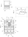
Figure 3 is a plan view of a power semiconductor device to which embodiments of the present description may apply, -
Figure 4 is a view of the portion ofFigure 3 indicated by the arrow IV, reproduced on an enlarged scale, -
Figure 5 is a view of the portion ofFigure 3 indicated by the arrow V, reproduced on an enlarged scale, -
Figures 6 to 12 (whereinFigure 7 is a cross-sectional view along line VII-VII ofFigure 6 ) are illustrative of a possible sequence of steps in manufacturing a semiconductor device, -
Figures 13 to 19 (whereinFigure 14 is a cross-sectional view along line XIV-XIV ofFigure 13 ) are illustrative of a possible sequence of steps in manufacturing a semiconductor device according to embodiments of the present description, -
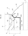
Figure 20 is a view of the portion ofFigure 19 indicated by the arrow XX, reproduced on an enlarged scale, -
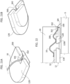
Figures 21A and 21B are perspective views illustrative of the possible result of the sequence of steps ofFigures 13 a 19, and -
Figure 22 is illustrative of a possible variant of embodiments of the present description. - Corresponding numerals and symbols in the different figures generally refer to corresponding parts unless otherwise indicated.
- The figures are drawn to clearly illustrate the relevant aspects of the embodiments and are not necessarily drawn to scale.
- The edges of features drawn in the figures do not necessarily indicate the termination of the extent of the feature.
- In the ensuing description one or more specific details are illustrated, aimed at providing an in-depth understanding of examples of embodiments of this description. The embodiments may be obtained without one or more of the specific details, or with other methods, components, materials, etc. In other cases, known structures, materials, or operations are not illustrated or described in detail so that certain aspects of embodiments will not be obscured.
- Reference to "an embodiment" or "one embodiment" in the framework of the present description is intended to indicate that a particular configuration, structure, or characteristic described in relation to the embodiment is comprised in at least one embodiment. Hence, phrases such as "in an embodiment" or "in one embodiment" that may be present in one or more points of the present description do not necessarily refer to one and the same embodiment.
- Moreover, particular conformations, structures, or characteristics may be combined in any adequate way in one or more embodiments.
- The headings/references used herein are provided merely for convenience and hence do not define the extent of protection or the scope of the embodiments.
- For simplicity and ease of explanation, throughout this description, and unless the context indicates otherwise, like parts or elements are indicated in the various figures with like reference signs, and a corresponding description will not be repeated for each and every figure.
-
Figure 1 is a partial cross-sectional view through asemiconductor device 10 mounted (attached) on a support member S such as a printed circuit broad, PCB. - As illustrated in
Figure 1 , attachment is via solder material SM and various device packages (e.g., for the automotive market) have ageometry feature 100 on the lead sides, called wettable flanks. - This feature facilitates formation of a meniscus in the solder material SM when soldering the
device 10 on a support member, e.g., PCB. - Wettable flanks facilitate automatic optical inspection insofar as the solder meniscus is visible.
- As illustrated herein by way of example, a semiconductor device such as the
device 10 comprises: - a substrate (leadframe) 12 having one or more (integrated circuit) semiconductor chips or
dice 14 arranged thereon, - electrically conductive formations (wires, ribbons, clips) 16 coupling the semiconductor chip(s) 14 to leads (outer pads) in the substrate, and
- an insulating encapsulation (e.g., a resin) 18 molded on the assembly thus formed to complete the plastic body of the
device 10. - As used herein, the terms chip/s and die/dice are regarded as synonymous
Figures 3 to 5 illustrate apower semiconductor device 10 comprising a low-power section (e.g., a controller die, illustrated on the right-hand side ofFigure 3 ) attached on a first die pad in theleadframe 12 and a high-power section (e.g., one or more power dice illustrated on the left-hand sideFigure 3 ) attached on one or more die pads in thelead frame 12, with an array of leads around the die pads having the low-power and the high-power dice mounted thereon. - The current transferred from the high-power section to the output pads of the device can be significant. As shown on the left-hand side of
Figure 3 , ribbons or clips 16 are thus used for that purpose in the place of wires. Wires, likewise indicated as 16 can still be used as shown on the right-hand side ofFigure 3 to provide electrical coupling to a low-power section (e.g., a controller) in the device. - The designation "leadframe" (or "lead frame") is currently used (see, for instance the USPC Consolidated Glossary of the United States Patent and Trademark Office) to indicate a metal frame that provides support for an integrated circuit chip or die as well as electrical leads to interconnect the integrated circuit in the die or chip to other electrical components or contacts.
- Essentially, a leadframe comprises an array of electrically-conductive formations (or leads, e.g., 12B) that from an outline location extend inwardly in the direction of a semiconductor chip or die (e.g., 14) thus forming an array of electrically-conductive formations from a die pad (e.g., 12A) configured to have at least one semiconductor chip or die attached thereon. This may be via conventional means such as a die attach adhesive (a die attach film or DAF, for instance).
- Again, as illustrated in
Figures 3 to 5 , electrically conductive formations are provided comprisingwire bonding patterns 16 coupling the low-power section (right-hand side ofFigure 3 ) to selected ones of theleads 12B and to the high-power section (left-hand side ofFigure 3 ) . These wire bonding patterns are coupled to die pads provided at the front or top surfaces of the chips. - Conversely, so-called ribbons are used to couple the high-power section (left-hand side of
Figure 3 ) to selected ones of theleads 12B acting as (power) output pads of thedevice 10. Using ribbons in the place of wires accounts for the fact that the current transferred from the high-power section to the output pads in a power semiconductor device may be significant. - A device structure as discussed so far is conventional in the art, which makes it unnecessary to provide a more detailed description herein.
- A single (integrated circuit) chip or die 14 mounted on a
single die pad 12A will be considered throughout the rest of this description for simplicity. - The
leadframe 12 is the base material support for thedevice 10. It is made of, e.g., copper, and shaped to accommodate semiconductor dice and generate pad connections. - Photo-etching can be advantageously used for leadframe manufacturing: a sheet or strip of copper material is etched on top and bottom side to create die pads and leads.
- Pads/leads are connected together by sacrificial connecting bars. Wedge-wedge bonding could be used to bond wires. Plating treatments are also applied as desired.
- Wedge(-wedge) bonding is a current designation for wire/ribbon bonding technology that use force and ultrasonic power in order to create an interconnection between a surface (e.g., a
leadframe 12/a die 14) and a wire/ribbon as designated by 16 in figures: in fact, Wedge bonding technology can be applied to both wires and ribbons. - As illustrated, e.g., in
Figures 4 and 5 , the (welded) connection of a wire and/orribbon 16 to a die/leadframe surface includes two sections: - a proximal section (wedge section proper) 161, and
- a distal section (tail formation) 162.
- The
proximal wedge section 161 carries the current/signal, whiledistal tail 162 does not contribute appreciably to signal transport, because that section is not welded to the die/leadframe surface. - After molding of the
encapsulation 18, the device package is sealed.Dice 14 and wires/ribbons 16 are no longer accessible from the outside. - Any detachment between a wire/
ribbon 16 and acorresponding lead 12B, for instance, will result in a failure of thewhole device 10. Wire bonding related issues may represent a major source of device failure. - A method to provide wettable flanks on a device package is by sawing.
- This approach relies on the fact that, in current manufacturing processes of semiconductor devices, plural devices are manufactured together and separated into single individual device in a final singulation (sawing) step.
- That is, after a chain of
devices 10 formed on a common leadframe strip is assembled (dice, wires and molding: seeFigures 6 and 7 ),individual devices 10 are separated via singulation as represented inFigure 10 using a sawing blade SB. - As illustrated in
Figures 8 and9 , prior to the final singulation, theleadframe 12 is partially sawn (engraved) using a circular saw SB' (this may be the same singulation blade SB or a different blade) that partially cuts the common leadframe strip material at pad (lead) level between adjacent devices, that is, at the device flanks. Pads (leads) remain connected together via connecting bars provide to facilitate electrical connection for plating. - Plating as indicated by 1200 is applied to the
whole leadframe 12 so that all exposed pad areas (diepads 12A and leads 12B) will be plated. - Final singulation as illustrated in
Figure 10 is then applied, cutting (e.g., via a saw SB) all the materials starting from the bottom or back surface of theleadframe 12 till the top of the package. As a result, each packageddevice 10 is separated from manufacturing chain. - As illustrated in
Figures 11 and 12 , adevice 10 thus produced will have an external flank surface plated area extending only on that part of the lead shape that does not derive from cutting during singulation: that portion of the wettable flanks produced from cutting (that is, that portion exposed as result of cutting during singulation, as indicated by 1000 inFigures 11 and 12 ) will have exposed - and unplated - leadframe material (copper) on the external package side. - As noted, solder SM is applied in order to connect the device package to a board S. Meniscus will appear after soldering.
- Electrical connection between the solder SM (the board S) and wire/
ribbon 16 takes place primarily through the metal (copper)lead 12B. In case of detachment betweenwire 16 and lead 12B, the device will likely fail with no possibility of recovery. - For simplicity a wire/lead is illustrated throughout
Figures 6 to 22 , but the same discussion also applies to a ribbon. - At least in principle, the risk of weld off/lift can be reduced keeping the assembly process as stable as possible, e.g., performing "in process control": input and output key parameters are checked according to a process control plan, and output parameters are monitored and checked (e.g., wire/ribbon pull and shear test). Electrical testing can also be envisaged.
- In process control is performed with a specific sample size and frequency: 100% checks are hardly feasible. Visual inspection of the connection between a wire and a lead can be performed before molding step only. Electrical testing can evaluate the interconnection during the test phase only: possible evolution and consequent failure of the interconnection cannot be predicted.
- Solutions as exemplified herein contemplate providing a recessed
region 200 in the front or top surface of theleads 12B and forming the wedge bond to the wire/ribbon 16 in such dedicated recessed region of the lead. - Such a recessed
area 200 can be provided, e.g., by chemical etching, coining, laser machining, or other conventional technologies known to those of skill in the art. For instance, such recessed areas orregions 200 can be formed at theleads 12B during leadframe manufacturing. - Such recessed areas or
regions 200 can have different shapes. - As visible in
Figures 16A and 16B (andFigures 21A and 21B - that refer to a condition after removal of the sacrificial tie bars 120B) the recessedportions 200 can be provided in individual leads 12B as a (e.g., rectangular) recess etched (in a manner known per se) in the metal (e.g., copper) of the sculptured structure of theleadframe 12. - It is noted that
Figures 16A and 16B (andFigures 21A and 21B as well) refer for clarity of representation: - to
individual leads 12B illustrated in isolation from any other neighboring part (e.g., the encapsulation 18) ; - to leads 12B shown after a final singulation step (see
Figure 18 ) that results in these etched recessed being cut about their half length, thus giving rise (in mutually facing leads 12B ofadjacent devices 10 manufactured simultaneously and then singulated) to half-recesses in the form of notches cut in the flanks of these devices. - It is further noted that the
leads 12B visible in the schematic representations ofFigures 16A and 16B (andFigures 21A and 21B ) have shapes that are different from theleads 12B ofFigures 3 to 5 orFigures 6 and13 . This is intended to highlight the possibility for solutions as discussed herein to be applied toleads 12B having a wide variety of shapes. - As noted, solutions as presented herein rely on the fact that in current manufacturing processes of semiconductor devices,
plural devices 10 are manufactured concurrently to be separated into single individual device in a final singulation (sawing) step. That is, after a chain ofdevices 10 formed on a common leadframe strip is assembled (dice, wires and molding: seeFigures 13 onwards),individual devices 10 are separated via singulation as represented inFigure 18 using a sawing blade SB. - Advantageously, the bond of the wire/
ribbon 16 to the recessedportion 200 at the proximal section 161 (this may be formed, e.g., as a "second bond" in a wire bonding process where a "first bond" is formed at the chip or die 14: see, e.g.,Figure 14 ) extends into a "long" distal,tail formation 162 long enough to cause thetail 162 to lie at (above) the wettable flank sawing area (see, e.g.,Figures 15 ,16A and 16B ). - The first sawing step (see SB' in dashed lines in
Figure 17 ) will cut through the (copper)lead 12B plus a portion of wire/ribbon thickness only, which is facilitated by a well-controlled sawing cut and relative wear of the blade SB'). - Electrical connection between pads (leads) can still be maintained via a sacrificial connecting
bar 120B that is still present. -
Plating 1200 is again applied over the whole (back or bottom surface) of leadframe, with exposed pad/lead areas plated. - Final singulation (see the blade SB in
Figure 19 ) will cut through the material thickness separating theindividual devices 10, removing the connectingbars 120B as well. - As visible in
Figure 20 , adevice 10 thus produced will again have an external flank surface plated area extending on that part of the lead shape that does not derive from cutting during singulation. - That external flank surface will comprise:
- a first (plated)
portion 1200A resulting from the first (partial) cutting through the lead 12B; - a second (plated)
portion 1200B resulting from the first (partial) cutting through (e.g., thetail 162 of) the wire/ribbon 16. - Only the end portion (e.g., the tail portion 162) of the wire/
ribbon 16 exposed as result of cutting during singulation will have exposed - and unplated - leadframe material (copper) on the external package side. - As visible in
Figures 21A and 21B (which represent the situation after removal of the sacrificial tie bars 120B) the recessedportions 200 can be provided in individual leads 12B as a (e.g., rectangular) recess etched (in a manner known per se) in the metal (e.g., copper) of the sculptured structure of theleadframe 12. - It is again noted that
Figures 21A and 21B refer, for clarity of representation, toindividual leads 12B illustrated in isolation from any other neighboring part (e.g., the encapsulation 18). - These leads 12B are shown after a final singulation step (see
Figure 18 ) that results in these etched recessed being cut about their half length, thus giving rise (in mutually facing leads 12B ofadjacent devices 10 manufactured simultaneously and then singulated) to half-recesses in the form of notches cut in the flanks of these devices. - The
final device 10 will thus have a plated area shape for wettable flanks (except for a small portion of wire/ribbon) on the external package side. - Solder can thus be applied to connect the
device 10 to the board S. Meniscus will be produced in the solder SM as a result of soldering. - As exemplified in
Figure 20 , electrical connection between the solder SM (the board S) and the wire/ribbon 16 will occur: - via the (copper)
lead 12B as exemplified by EC1, and - via an additional connection path between the wire/
ribbon 16 and the solder SM as exemplified by EC2. - In case of detachment between the wire/
ribbon 16 and the lead 12B (connection EC1 fail), thedevice 10 can remain operable through the solder to wire/ribbon 16 connection (connection EC2). - To summarize, solutions as presented herein involve arranging at least one semiconductor die 14 on a
die pad 12A at a first surface of a support substrate (leadframe) 12. - The
support substrate 12 has a first thickness (indicated as T1 in the figures) between the first surface and a second surface opposite the first surface. - The support substrate (leadframe) 12 comprises an array of electrically conductive leads 12B around the
die pad 12A. - Terminal recesses 200 (that is, recesses located at or in proximity of the distal end of the lead 12B concerned) are formed in (at least some of) the electrically conductive leads 12B in the array at the first surface of the leadframe 12 (that is, the surface onto which the
die 14 is mounted). - At the terminal recesses 200, the
leads 12B have a second thickness (indicated as T2 in the figures) that is less than the first thickness T1. - The electrically conductive, elongated formations such as the wires or
ribbons 16 have coupling ends 161, 162 to the electrically conductive leads 12B arranged at therecesses 200. - Partially cutting (engraving) the
leadframe 12 starting from the second surface as presented by reference SB' is carried out at theterminal recesses 200 with a cutting thickness Tx (depth) that lies between the first thickness T1 and the second thickness T2 (T1 > Tx > T2) . - Partial cutting SB' thus produces exposed surfaces of the support substrate (see
reference 1200A) and the coupling ends (seereference 1200B) of the wires orribbons 16. - The insulating
encapsulation 18 molded onto the semiconductor die 14 arranged on thedie pad 12A at the first surface of thesupport substrate 12 leaves uncovered (as solder wettable flanks) the exposed surfaces of thesupport substrate 1200A and the coupling ends 1200B of the electrically conductiveelongated formations 16 produced by partial cutting. - As illustrated, the coupling ends 161, 162 of the wires or
ribbons 16 torespective leads 12B, comprise, arranged in the terminal recesses 200: - proximal portions 161 (e.g., wedge) bonded to selected ones of the electrically conductive leads 12B at the
recesses 200, and -
distal portions 162 projecting from theproximal portions 161 at therecesses 200. - As illustrated, the
distal portions 162 are exempt from bonding to theleads 12B. - Advantageously, partial cutting SB' at the
terminal recesses 200 with a cutting thickness between the first thickness (T1) and the second thickness (T2) takes place at thedistal portions 162, thus producing exposed surfaces of the support substrate (leadframe, seereference 1200A) and of thedistal portions 162 the coupling ends of the wires orribbons 16. - As exemplified in
Figures 19 and20 , thedevice 10 with thesupport substrate 12 having the semiconductor die ordice 14 arranged on thedie pad 12A can be mounted onto a mounting member (such as a printed circuit board S) via solder material SM that wets and forms a solder meniscus at both exposed surfaces of the leadframe 12 (seereference 1200A) and of the coupling ends (seereference 1200B) of the wires orribbons 16. - Embodiments as presented herein can be applied to any package that use a wire or ribbon welded through wedge-wedge bonding technology and take advantage from having a wettable flank.
-
Figure 22 is illustrative of a possible variant of embodiments of the present description where double or plural bonding is applied, e.g., to awire 16. - It will be appreciated that the (first, partial) sawing line SB' can pass through
proximal section 161 of the bond, thus also in the absence of a "long" distal,tail formation 162. - Wedge(-wedge) bonding as discussed herein can be performed using wires or ribbons made of aluminum, copper, gold or other materials suited to be bonded, e.g., with an ultrasonic process.
- Solutions as discussed herein provide improved package reliability, e.g., as a result of solder meniscus SM directly connected to the wire/
ribbon 16. - No additional process steps or costs are involved: solutions as discussed herein can be implemented using existing wire bonding machines.
- Wire/ribbon tails can be made accessible from the outside of the device package. Wettable flanks may have a direct connection between wire and solder, when mounted on board.
- Wettable flanks are a desirable specification of certain automotive products.
- Wettable flanks facilitate automatic inspection in order to check the correct welding of the package to the board.
- Using wedge bonding technology together with a special lead design (recessed area), facilitates exposing a wire or ribbon portion (e.g., a "tail") outside the package sides. Those portions can be incorporated together with the leads by the solder, when a device is assembled on a board. In that way, the wires/ribbons are connected with respective leads and with the solder as well. In case a first connection (e.g., EC1) fails for any reason (wedge lift), a second connection (e.g., EC2) can compensate the first, thus maintaining device operation. Device reliability is improved.
- Visual inspection on the package side (and/or 3D x-ray analysis), possibly facilitated by cross-section and/or decapsulation can reveal the lead recessed
areas 200. - Without prejudice to the underlying principles, the details and embodiments may vary, even significantly, with respect to what has been described by way of example only without departing from the extent of protection.
- The extent of protection is determined by the annexed claims.
Claims (13)
- A method, comprising:arranging at least one semiconductor die (14) on a die pad (12A) at a first surface of a support substrate (12), the support substrate (12) having a first thickness (T1) between the first surface and a second surface opposite the first surface and comprising an array of electrically conductive leads (12B) around the die pad (12A), wherein electrically conductive leads (12B) in the array of electrically conductive leads (12B) have terminal recesses (200) at the first surface of the support substrate (12), wherein at said terminal recesses (200) said electrically conductive leads (12B) in the array of electrically conductive leads (12B) have a second thickness (T2) less than said first thickness (T1),electrically coupling (16) the at least one semiconductor die (14) with said electrically conductive leads (12B) in the array of electrically conductive leads (12B) via electrically conductive elongated formations (16) having coupling ends (161, 162) to the electrically conductive leads (12B) in the array of electrically conductive leads (12B) arranged in said terminal recesses (200), andpartially cutting (SB') the support substrate (12) starting from the second surface, partially cutting (SB') being at said terminal recesses (200) and with a cutting thickness between the first thickness (T1) and the second thickness (T2), wherein the partial cutting (SB') produces exposed surfaces of the support substrate (1200A) and the coupling ends (1200B) of the electrically conductive elongated formations (16).
- The method of claim 1, comprising molding an insulating encapsulation (18) onto the at least one semiconductor die (14) arranged on the die pad (12A) at the first surface of the support substrate (12), wherein the insulating encapsulation (18) leaves uncovered the exposed surfaces of the support substrate (1200A) and the coupling ends (1200B) of the electrically conductive elongated formations (16) produced by said partially cutting (SB').
- The method of claim 1, wherein the electrically conductive elongated formations (16) having coupling ends (161, 162) arranged in said terminal recesses (200) comprise wires or ribbons.
- The method of any of the previous claims, wherein said coupling ends (161, 162) of the electrically conductive elongated formations (16) to the electrically conductive leads (12B) in the array of electrically conductive leads (12B) arranged in said terminal recesses (200) comprise:proximal portions (161) bonded to electrically conductive leads (12B) in the array of electrically conductive leads (12B) at said recesses (200), anddistal portions (162) projecting distally of the proximal portions (161) at said recesses (200) in the absence of bonding of the distal portion (162) to electrically conductive leads (12B) in the array of electrically conductive leads (12B).
- The method of claim 4, comprising wedge bonding said proximal portions (161) to electrically conductive leads (12B) in the array of electrically conductive leads (12B) at said recesses (200).
- The method of claim 4 or claim 5, wherein partially cutting (SB') at said terminal recesses (200) with a cutting thickness between the first thickness (T1) and the second thickness (T2) is at said distal portions (162) wherein the partial cutting (SB') produces exposed surfaces of the support substrate (1200A) and of the distal portions (162) of the coupling ends of the electrically conductive elongated formations (16) .
- The method of any of the previous claims, comprising mounting the support substrate (12) having the at least one semiconductor die (14) arranged on the die pad (12A) onto a mounting member (S) via solder material (SM) that wets and forms a solder meniscus at both exposed surfaces of the support substrate (1200A) and of the coupling ends (1200B) of the electrically conductive elongated formations (16).
- A device (10), comprising:at least one semiconductor die (14) arranged on a die pad (12A) at a first surface of a support substrate (12), the support substrate (12) having a first thickness (T1) between the first surface and a second surface opposite the first surface and comprising an array of electrically conductive leads (12B) around the die pad (12A),terminal recesses (200) in electrically conductive leads (12B) in the array of electrically conductive leads (12B) at the first surface of the support substrate (12), wherein at said terminal recesses (200) said electrically conductive leads (12B) in the array of electrically conductive leads (12B) have a second thickness (T2) less than said first thickness (T1),electrically conductive elongated formations (16) electrically coupling (16) the at least one semiconductor die (14) with said electrically conductive leads (12B) in the array of electrically conductive leads (12B), the electrically conductive elongated formations (16) having coupling ends (161, 162) to the electrically conductive leads (12B) in the array of electrically conductive leads (12B) arranged in said terminal recesses (200), anda partial cut (SB') in the support substrate (12) starting from the second surface, the partial cut (SB') being at said terminal recesses (200) and with a cutting depth between the first thickness (T1) and the second thickness (T2), wherein the partial cut (SB') leaves exposed surfaces of the support substrate (1200A) and the coupling ends (1200B) of the electrically conductive elongated formations (16).
- The device (10) of claim 8, comprising an insulating encapsulation (18) molded onto the at least one semiconductor die (14) arranged on the die pad (12A) at the first surface of the support substrate (12), wherein the insulating encapsulation (18) leaves uncovered the exposed surfaces of the support substrate (1200A) and the coupling ends (1200B) of the electrically conductive elongated formations (16).
- The device (10) of claim 8 or claim 9, wherein the electrically conductive elongated formations (16) having coupling ends (161, 162) arranged in said terminal recesses (200) comprise wires or ribbons.
- The device (10) of any of claims 8 to 10, wherein said coupling ends (161, 162) to the electrically conductive leads (12B) in the array of electrically conductive leads (12B) arranged in said terminal recesses (200) comprise:proximal portions (161) bonded, preferably wedgebonded, to electrically conductive leads (12B) in the array of electrically conductive leads (12B) at said recesses (200), anddistal portions (162) projecting distally of the proximal portions (161) at said recesses (200) in the absence of bonding of the distal portion (162) to electrically conductive leads (12B) in the array of electrically conductive leads (12B).
- An assembly comprising,a semiconductor device mounting member (S), anda device (10) according to any of claims 8 to 11 mounted onto said mounting member (S) via solder material (SM) exhibiting a solder meniscus at both exposed surfaces of the support substrate (1200A) and of the coupling ends (1200B) of the electrically conductive elongated formations (16).
- A support substrate (12) for use in the method of any of claims 1 to 7, the support substrate (12) having said first thickness (T1) between the first surface and the second surface opposite the first surface and comprising said array of electrically conductive leads (12B) around the die pad (12A), the support substrate (12) having terminal recesses (200) in electrically conductive leads (12B) in the array of electrically conductive leads (12B) at the first surface of the support substrate (12), wherein at said terminal recesses (200) said electrically conductive leads (12B) in the array of electrically conductive leads (12B) have a second thickness (T2) less than said first thickness (T1), said terminal recesses (200) configured to have arranged therein the coupling ends (161, 162) of the electrically conductive elongated formations (16) that electrically couple (16) the at least one semiconductor die (14) with said electrically conductive leads (12B) in the array of electrically conductive leads (12B).
Applications Claiming Priority (1)
| Application Number | Priority Date | Filing Date | Title |
|---|---|---|---|
| IT202200022422 | 2022-11-02 |
Publications (2)
| Publication Number | Publication Date |
|---|---|
| EP4376072A1 true EP4376072A1 (en) | 2024-05-29 |
| EP4376072B1 EP4376072B1 (en) | 2025-07-30 |
Family
ID=84785022
Family Applications (1)
| Application Number | Title | Priority Date | Filing Date |
|---|---|---|---|
| EP23203555.0A Active EP4376072B1 (en) | 2022-11-02 | 2023-10-13 | Method of manufacturing semiconductor devices, corresponding semiconductor device, assembly and support substrate |
Country Status (3)
| Country | Link |
|---|---|
| US (1) | US20240145351A1 (en) |
| EP (1) | EP4376072B1 (en) |
| CN (2) | CN117995694A (en) |
Citations (3)
| Publication number | Priority date | Publication date | Assignee | Title |
|---|---|---|---|---|
| JPH11145369A (en) | 1997-11-07 | 1999-05-28 | Hitachi Ltd | Lead frame, semiconductor device using the same, and method of manufacturing the same |
| JP2010050491A (en) | 2009-12-02 | 2010-03-04 | Renesas Technology Corp | Method of manufacturing semiconductor device |
| US20160254214A1 (en) | 2014-03-27 | 2016-09-01 | Renesas Electronics Corporaton | Method of manufacturing semiconductor device and semiconductor device |
-
2023
- 2023-10-13 EP EP23203555.0A patent/EP4376072B1/en active Active
- 2023-10-27 US US18/384,524 patent/US20240145351A1/en active Pending
- 2023-11-02 CN CN202311448791.XA patent/CN117995694A/en active Pending
- 2023-11-02 CN CN202322972240.5U patent/CN221727104U/en active Active
Patent Citations (3)
| Publication number | Priority date | Publication date | Assignee | Title |
|---|---|---|---|---|
| JPH11145369A (en) | 1997-11-07 | 1999-05-28 | Hitachi Ltd | Lead frame, semiconductor device using the same, and method of manufacturing the same |
| JP2010050491A (en) | 2009-12-02 | 2010-03-04 | Renesas Technology Corp | Method of manufacturing semiconductor device |
| US20160254214A1 (en) | 2014-03-27 | 2016-09-01 | Renesas Electronics Corporaton | Method of manufacturing semiconductor device and semiconductor device |
Also Published As
| Publication number | Publication date |
|---|---|
| CN221727104U (en) | 2024-09-17 |
| EP4376072B1 (en) | 2025-07-30 |
| CN117995694A (en) | 2024-05-07 |
| US20240145351A1 (en) | 2024-05-02 |
Similar Documents
| Publication | Publication Date | Title |
|---|---|---|
| JP5634033B2 (en) | Resin-sealed semiconductor device and manufacturing method thereof | |
| KR102178587B1 (en) | Method for manufacturing semiconductor device and semiconductor device | |
| JP5959386B2 (en) | Resin-sealed semiconductor device and manufacturing method thereof | |
| JP3862410B2 (en) | Semiconductor device manufacturing method and structure thereof | |
| US8076181B1 (en) | Lead plating technique for singulated IC packages | |
| JP3547704B2 (en) | Lead frame and semiconductor device | |
| KR0179920B1 (en) | Method of manufacturing chip-size package | |
| CN113614879B (en) | Semiconductor package with sidewall plating | |
| KR20050065340A (en) | A method of manufacturing a semiconductor device | |
| KR20160075316A (en) | Lead frame and semi-conductor device | |
| JP7144157B2 (en) | Semiconductor device and its manufacturing method | |
| CN113035722A (en) | Packaging process for plating with selective molding | |
| EP4376072B1 (en) | Method of manufacturing semiconductor devices, corresponding semiconductor device, assembly and support substrate | |
| KR0175417B1 (en) | Semiconductor device and manufacture thereof | |
| JP2004228166A (en) | Semiconductor device and manufacturing method thereof | |
| JP7674930B2 (en) | Lead frame, semiconductor device, and method of manufacturing lead frame | |
| JP6143726B2 (en) | Resin-encapsulated semiconductor device, manufacturing method thereof, lead frame | |
| KR20020093250A (en) | ELP type leadframe and ELP using the same | |
| TWI900363B (en) | Method for forming non-leaded semiconductor package device | |
| US20250149410A1 (en) | Semiconductor device and method of manufacturing the same | |
| US20250014982A1 (en) | Method of manufacturing semiconductor devices, corresponding pre-molded leadframe and semiconductor device | |
| JP2002164496A (en) | Semiconductor device and manufacturing method thereof | |
| JP3482900B2 (en) | Manufacturing method of BGA type semiconductor device | |
| JP2025174697A (en) | Semiconductor device and manufacturing method thereof | |
| HK40055221A (en) | Packaging process for plating with selective molding |
Legal Events
| Date | Code | Title | Description |
|---|---|---|---|
| PUAI | Public reference made under article 153(3) epc to a published international application that has entered the european phase |
Free format text: ORIGINAL CODE: 0009012 |
|
| STAA | Information on the status of an ep patent application or granted ep patent |
Free format text: STATUS: THE APPLICATION HAS BEEN PUBLISHED |
|
| AK | Designated contracting states |
Kind code of ref document: A1 Designated state(s): AL AT BE BG CH CY CZ DE DK EE ES FI FR GB GR HR HU IE IS IT LI LT LU LV MC ME MK MT NL NO PL PT RO RS SE SI SK SM TR |
|
| STAA | Information on the status of an ep patent application or granted ep patent |
Free format text: STATUS: REQUEST FOR EXAMINATION WAS MADE |
|
| 17P | Request for examination filed |
Effective date: 20240902 |
|
| RBV | Designated contracting states (corrected) |
Designated state(s): AL AT BE BG CH CY CZ DE DK EE ES FI FR GB GR HR HU IE IS IT LI LT LU LV MC ME MK MT NL NO PL PT RO RS SE SI SK SM TR |
|
| GRAP | Despatch of communication of intention to grant a patent |
Free format text: ORIGINAL CODE: EPIDOSNIGR1 |
|
| STAA | Information on the status of an ep patent application or granted ep patent |
Free format text: STATUS: GRANT OF PATENT IS INTENDED |
|
| INTG | Intention to grant announced |
Effective date: 20250303 |
|
| RIN1 | Information on inventor provided before grant (corrected) |
Inventor name: MAZZOLA, MAURO Inventor name: DE SANTA, MATTEO |
|
| GRAS | Grant fee paid |
Free format text: ORIGINAL CODE: EPIDOSNIGR3 |
|
| GRAA | (expected) grant |
Free format text: ORIGINAL CODE: 0009210 |
|
| STAA | Information on the status of an ep patent application or granted ep patent |
Free format text: STATUS: THE PATENT HAS BEEN GRANTED |
|
| AK | Designated contracting states |
Kind code of ref document: B1 Designated state(s): AL AT BE BG CH CY CZ DE DK EE ES FI FR GB GR HR HU IE IS IT LI LT LU LV MC ME MK MT NL NO PL PT RO RS SE SI SK SM TR |
|
| REG | Reference to a national code |
Ref country code: GB Ref legal event code: FG4D |
|
| REG | Reference to a national code |
Ref country code: CH Ref legal event code: EP |
|
| REG | Reference to a national code |
Ref country code: DE Ref legal event code: R096 Ref document number: 602023005221 Country of ref document: DE |
|
| REG | Reference to a national code |
Ref country code: IE Ref legal event code: FG4D |
|
| REG | Reference to a national code |
Ref country code: DE Ref legal event code: R079 Ref document number: 602023005221 Country of ref document: DE Free format text: PREVIOUS MAIN CLASS: H01L0023495000 Ipc: H10W0070400000 |
|
| REG | Reference to a national code |
Ref country code: NL Ref legal event code: MP Effective date: 20250730 |
|
| REG | Reference to a national code |
Ref country code: AT Ref legal event code: MK05 Ref document number: 1820011 Country of ref document: AT Kind code of ref document: T Effective date: 20250730 |
|
| PG25 | Lapsed in a contracting state [announced via postgrant information from national office to epo] |
Ref country code: PT Free format text: LAPSE BECAUSE OF FAILURE TO SUBMIT A TRANSLATION OF THE DESCRIPTION OR TO PAY THE FEE WITHIN THE PRESCRIBED TIME-LIMIT Effective date: 20251202 |
|
| PG25 | Lapsed in a contracting state [announced via postgrant information from national office to epo] |
Ref country code: IS Free format text: LAPSE BECAUSE OF FAILURE TO SUBMIT A TRANSLATION OF THE DESCRIPTION OR TO PAY THE FEE WITHIN THE PRESCRIBED TIME-LIMIT Effective date: 20251130 |
|
| PGFP | Annual fee paid to national office [announced via postgrant information from national office to epo] |
Ref country code: DE Payment date: 20250923 Year of fee payment: 3 |
|
| PG25 | Lapsed in a contracting state [announced via postgrant information from national office to epo] |
Ref country code: NO Free format text: LAPSE BECAUSE OF FAILURE TO SUBMIT A TRANSLATION OF THE DESCRIPTION OR TO PAY THE FEE WITHIN THE PRESCRIBED TIME-LIMIT Effective date: 20251030 |
|
| REG | Reference to a national code |
Ref country code: LT Ref legal event code: MG9D |
|
| PG25 | Lapsed in a contracting state [announced via postgrant information from national office to epo] |
Ref country code: AT Free format text: LAPSE BECAUSE OF FAILURE TO SUBMIT A TRANSLATION OF THE DESCRIPTION OR TO PAY THE FEE WITHIN THE PRESCRIBED TIME-LIMIT Effective date: 20250730 |
|
| PG25 | Lapsed in a contracting state [announced via postgrant information from national office to epo] |
Ref country code: FI Free format text: LAPSE BECAUSE OF FAILURE TO SUBMIT A TRANSLATION OF THE DESCRIPTION OR TO PAY THE FEE WITHIN THE PRESCRIBED TIME-LIMIT Effective date: 20250730 |
|
| PG25 | Lapsed in a contracting state [announced via postgrant information from national office to epo] |
Ref country code: NL Free format text: LAPSE BECAUSE OF FAILURE TO SUBMIT A TRANSLATION OF THE DESCRIPTION OR TO PAY THE FEE WITHIN THE PRESCRIBED TIME-LIMIT Effective date: 20250730 Ref country code: HR Free format text: LAPSE BECAUSE OF FAILURE TO SUBMIT A TRANSLATION OF THE DESCRIPTION OR TO PAY THE FEE WITHIN THE PRESCRIBED TIME-LIMIT Effective date: 20250730 |
|
| PG25 | Lapsed in a contracting state [announced via postgrant information from national office to epo] |
Ref country code: GR Free format text: LAPSE BECAUSE OF FAILURE TO SUBMIT A TRANSLATION OF THE DESCRIPTION OR TO PAY THE FEE WITHIN THE PRESCRIBED TIME-LIMIT Effective date: 20251031 |
|
| PG25 | Lapsed in a contracting state [announced via postgrant information from national office to epo] |
Ref country code: SE Free format text: LAPSE BECAUSE OF FAILURE TO SUBMIT A TRANSLATION OF THE DESCRIPTION OR TO PAY THE FEE WITHIN THE PRESCRIBED TIME-LIMIT Effective date: 20250730 |
|
| PG25 | Lapsed in a contracting state [announced via postgrant information from national office to epo] |
Ref country code: LV Free format text: LAPSE BECAUSE OF FAILURE TO SUBMIT A TRANSLATION OF THE DESCRIPTION OR TO PAY THE FEE WITHIN THE PRESCRIBED TIME-LIMIT Effective date: 20250730 |
|
| PG25 | Lapsed in a contracting state [announced via postgrant information from national office to epo] |
Ref country code: PL Free format text: LAPSE BECAUSE OF FAILURE TO SUBMIT A TRANSLATION OF THE DESCRIPTION OR TO PAY THE FEE WITHIN THE PRESCRIBED TIME-LIMIT Effective date: 20250730 Ref country code: BG Free format text: LAPSE BECAUSE OF FAILURE TO SUBMIT A TRANSLATION OF THE DESCRIPTION OR TO PAY THE FEE WITHIN THE PRESCRIBED TIME-LIMIT Effective date: 20250730 |
|
| PG25 | Lapsed in a contracting state [announced via postgrant information from national office to epo] |
Ref country code: RS Free format text: LAPSE BECAUSE OF FAILURE TO SUBMIT A TRANSLATION OF THE DESCRIPTION OR TO PAY THE FEE WITHIN THE PRESCRIBED TIME-LIMIT Effective date: 20251030 |
|
| PG25 | Lapsed in a contracting state [announced via postgrant information from national office to epo] |
Ref country code: ES Free format text: LAPSE BECAUSE OF FAILURE TO SUBMIT A TRANSLATION OF THE DESCRIPTION OR TO PAY THE FEE WITHIN THE PRESCRIBED TIME-LIMIT Effective date: 20250730 |
|
| PG25 | Lapsed in a contracting state [announced via postgrant information from national office to epo] |
Ref country code: RO Free format text: LAPSE BECAUSE OF FAILURE TO SUBMIT A TRANSLATION OF THE DESCRIPTION OR TO PAY THE FEE WITHIN THE PRESCRIBED TIME-LIMIT Effective date: 20250730 |
|
| PG25 | Lapsed in a contracting state [announced via postgrant information from national office to epo] |
Ref country code: SM Free format text: LAPSE BECAUSE OF FAILURE TO SUBMIT A TRANSLATION OF THE DESCRIPTION OR TO PAY THE FEE WITHIN THE PRESCRIBED TIME-LIMIT Effective date: 20250730 |
|
| PG25 | Lapsed in a contracting state [announced via postgrant information from national office to epo] |
Ref country code: DK Free format text: LAPSE BECAUSE OF FAILURE TO SUBMIT A TRANSLATION OF THE DESCRIPTION OR TO PAY THE FEE WITHIN THE PRESCRIBED TIME-LIMIT Effective date: 20250730 |
|
| PG25 | Lapsed in a contracting state [announced via postgrant information from national office to epo] |
Ref country code: IT Free format text: LAPSE BECAUSE OF FAILURE TO SUBMIT A TRANSLATION OF THE DESCRIPTION OR TO PAY THE FEE WITHIN THE PRESCRIBED TIME-LIMIT Effective date: 20250730 |
|
| PG25 | Lapsed in a contracting state [announced via postgrant information from national office to epo] |
Ref country code: CZ Free format text: LAPSE BECAUSE OF FAILURE TO SUBMIT A TRANSLATION OF THE DESCRIPTION OR TO PAY THE FEE WITHIN THE PRESCRIBED TIME-LIMIT Effective date: 20250730 |
|
| PG25 | Lapsed in a contracting state [announced via postgrant information from national office to epo] |
Ref country code: EE Free format text: LAPSE BECAUSE OF FAILURE TO SUBMIT A TRANSLATION OF THE DESCRIPTION OR TO PAY THE FEE WITHIN THE PRESCRIBED TIME-LIMIT Effective date: 20250730 Ref country code: SK Free format text: LAPSE BECAUSE OF FAILURE TO SUBMIT A TRANSLATION OF THE DESCRIPTION OR TO PAY THE FEE WITHIN THE PRESCRIBED TIME-LIMIT Effective date: 20250730 |