EP4375740A1 - Backlight unit and liquid crystal display device - Google Patents
Backlight unit and liquid crystal display device Download PDFInfo
- Publication number
- EP4375740A1 EP4375740A1 EP23208136.4A EP23208136A EP4375740A1 EP 4375740 A1 EP4375740 A1 EP 4375740A1 EP 23208136 A EP23208136 A EP 23208136A EP 4375740 A1 EP4375740 A1 EP 4375740A1
- Authority
- EP
- European Patent Office
- Prior art keywords
- sheet
- backlight unit
- liquid crystal
- cutouts
- reflector
- Prior art date
- Legal status (The legal status is an assumption and is not a legal conclusion. Google has not performed a legal analysis and makes no representation as to the accuracy of the status listed.)
- Granted
Links
Images





Classifications
-
- G—PHYSICS
- G02—OPTICS
- G02F—OPTICAL DEVICES OR ARRANGEMENTS FOR THE CONTROL OF LIGHT BY MODIFICATION OF THE OPTICAL PROPERTIES OF THE MEDIA OF THE ELEMENTS INVOLVED THEREIN; NON-LINEAR OPTICS; FREQUENCY-CHANGING OF LIGHT; OPTICAL LOGIC ELEMENTS; OPTICAL ANALOGUE/DIGITAL CONVERTERS
- G02F1/00—Devices or arrangements for the control of the intensity, colour, phase, polarisation or direction of light arriving from an independent light source, e.g. switching, gating or modulating; Non-linear optics
- G02F1/01—Devices or arrangements for the control of the intensity, colour, phase, polarisation or direction of light arriving from an independent light source, e.g. switching, gating or modulating; Non-linear optics for the control of the intensity, phase, polarisation or colour
- G02F1/13—Devices or arrangements for the control of the intensity, colour, phase, polarisation or direction of light arriving from an independent light source, e.g. switching, gating or modulating; Non-linear optics for the control of the intensity, phase, polarisation or colour based on liquid crystals, e.g. single liquid crystal display cells
- G02F1/133—Constructional arrangements; Operation of liquid crystal cells; Circuit arrangements
- G02F1/1333—Constructional arrangements; Manufacturing methods
- G02F1/1335—Structural association of cells with optical devices, e.g. polarisers or reflectors
- G02F1/1336—Illuminating devices
- G02F1/133602—Direct backlight
- G02F1/133605—Direct backlight including specially adapted reflectors
-
- G—PHYSICS
- G02—OPTICS
- G02F—OPTICAL DEVICES OR ARRANGEMENTS FOR THE CONTROL OF LIGHT BY MODIFICATION OF THE OPTICAL PROPERTIES OF THE MEDIA OF THE ELEMENTS INVOLVED THEREIN; NON-LINEAR OPTICS; FREQUENCY-CHANGING OF LIGHT; OPTICAL LOGIC ELEMENTS; OPTICAL ANALOGUE/DIGITAL CONVERTERS
- G02F1/00—Devices or arrangements for the control of the intensity, colour, phase, polarisation or direction of light arriving from an independent light source, e.g. switching, gating or modulating; Non-linear optics
- G02F1/01—Devices or arrangements for the control of the intensity, colour, phase, polarisation or direction of light arriving from an independent light source, e.g. switching, gating or modulating; Non-linear optics for the control of the intensity, phase, polarisation or colour
- G02F1/13—Devices or arrangements for the control of the intensity, colour, phase, polarisation or direction of light arriving from an independent light source, e.g. switching, gating or modulating; Non-linear optics for the control of the intensity, phase, polarisation or colour based on liquid crystals, e.g. single liquid crystal display cells
- G02F1/133—Constructional arrangements; Operation of liquid crystal cells; Circuit arrangements
- G02F1/1333—Constructional arrangements; Manufacturing methods
- G02F1/133308—Support structures for LCD panels, e.g. frames or bezels
- G02F1/133314—Back frames
-
- G—PHYSICS
- G02—OPTICS
- G02F—OPTICAL DEVICES OR ARRANGEMENTS FOR THE CONTROL OF LIGHT BY MODIFICATION OF THE OPTICAL PROPERTIES OF THE MEDIA OF THE ELEMENTS INVOLVED THEREIN; NON-LINEAR OPTICS; FREQUENCY-CHANGING OF LIGHT; OPTICAL LOGIC ELEMENTS; OPTICAL ANALOGUE/DIGITAL CONVERTERS
- G02F1/00—Devices or arrangements for the control of the intensity, colour, phase, polarisation or direction of light arriving from an independent light source, e.g. switching, gating or modulating; Non-linear optics
- G02F1/01—Devices or arrangements for the control of the intensity, colour, phase, polarisation or direction of light arriving from an independent light source, e.g. switching, gating or modulating; Non-linear optics for the control of the intensity, phase, polarisation or colour
- G02F1/13—Devices or arrangements for the control of the intensity, colour, phase, polarisation or direction of light arriving from an independent light source, e.g. switching, gating or modulating; Non-linear optics for the control of the intensity, phase, polarisation or colour based on liquid crystals, e.g. single liquid crystal display cells
- G02F1/133—Constructional arrangements; Operation of liquid crystal cells; Circuit arrangements
- G02F1/1333—Constructional arrangements; Manufacturing methods
- G02F1/133308—Support structures for LCD panels, e.g. frames or bezels
- G02F1/133322—Mechanical guidance or alignment of LCD panel support components
-
- G—PHYSICS
- G02—OPTICS
- G02F—OPTICAL DEVICES OR ARRANGEMENTS FOR THE CONTROL OF LIGHT BY MODIFICATION OF THE OPTICAL PROPERTIES OF THE MEDIA OF THE ELEMENTS INVOLVED THEREIN; NON-LINEAR OPTICS; FREQUENCY-CHANGING OF LIGHT; OPTICAL LOGIC ELEMENTS; OPTICAL ANALOGUE/DIGITAL CONVERTERS
- G02F1/00—Devices or arrangements for the control of the intensity, colour, phase, polarisation or direction of light arriving from an independent light source, e.g. switching, gating or modulating; Non-linear optics
- G02F1/01—Devices or arrangements for the control of the intensity, colour, phase, polarisation or direction of light arriving from an independent light source, e.g. switching, gating or modulating; Non-linear optics for the control of the intensity, phase, polarisation or colour
- G02F1/13—Devices or arrangements for the control of the intensity, colour, phase, polarisation or direction of light arriving from an independent light source, e.g. switching, gating or modulating; Non-linear optics for the control of the intensity, phase, polarisation or colour based on liquid crystals, e.g. single liquid crystal display cells
- G02F1/133—Constructional arrangements; Operation of liquid crystal cells; Circuit arrangements
- G02F1/1333—Constructional arrangements; Manufacturing methods
- G02F1/1335—Structural association of cells with optical devices, e.g. polarisers or reflectors
- G02F1/1336—Illuminating devices
- G02F1/133602—Direct backlight
- G02F1/133603—Direct backlight with LEDs
-
- G—PHYSICS
- G02—OPTICS
- G02F—OPTICAL DEVICES OR ARRANGEMENTS FOR THE CONTROL OF LIGHT BY MODIFICATION OF THE OPTICAL PROPERTIES OF THE MEDIA OF THE ELEMENTS INVOLVED THEREIN; NON-LINEAR OPTICS; FREQUENCY-CHANGING OF LIGHT; OPTICAL LOGIC ELEMENTS; OPTICAL ANALOGUE/DIGITAL CONVERTERS
- G02F1/00—Devices or arrangements for the control of the intensity, colour, phase, polarisation or direction of light arriving from an independent light source, e.g. switching, gating or modulating; Non-linear optics
- G02F1/01—Devices or arrangements for the control of the intensity, colour, phase, polarisation or direction of light arriving from an independent light source, e.g. switching, gating or modulating; Non-linear optics for the control of the intensity, phase, polarisation or colour
- G02F1/13—Devices or arrangements for the control of the intensity, colour, phase, polarisation or direction of light arriving from an independent light source, e.g. switching, gating or modulating; Non-linear optics for the control of the intensity, phase, polarisation or colour based on liquid crystals, e.g. single liquid crystal display cells
- G02F1/133—Constructional arrangements; Operation of liquid crystal cells; Circuit arrangements
- G02F1/1333—Constructional arrangements; Manufacturing methods
- G02F1/1335—Structural association of cells with optical devices, e.g. polarisers or reflectors
- G02F1/1336—Illuminating devices
- G02F1/133602—Direct backlight
- G02F1/133606—Direct backlight including a specially adapted diffusing, scattering or light controlling members
-
- G—PHYSICS
- G02—OPTICS
- G02F—OPTICAL DEVICES OR ARRANGEMENTS FOR THE CONTROL OF LIGHT BY MODIFICATION OF THE OPTICAL PROPERTIES OF THE MEDIA OF THE ELEMENTS INVOLVED THEREIN; NON-LINEAR OPTICS; FREQUENCY-CHANGING OF LIGHT; OPTICAL LOGIC ELEMENTS; OPTICAL ANALOGUE/DIGITAL CONVERTERS
- G02F1/00—Devices or arrangements for the control of the intensity, colour, phase, polarisation or direction of light arriving from an independent light source, e.g. switching, gating or modulating; Non-linear optics
- G02F1/01—Devices or arrangements for the control of the intensity, colour, phase, polarisation or direction of light arriving from an independent light source, e.g. switching, gating or modulating; Non-linear optics for the control of the intensity, phase, polarisation or colour
- G02F1/13—Devices or arrangements for the control of the intensity, colour, phase, polarisation or direction of light arriving from an independent light source, e.g. switching, gating or modulating; Non-linear optics for the control of the intensity, phase, polarisation or colour based on liquid crystals, e.g. single liquid crystal display cells
- G02F1/133—Constructional arrangements; Operation of liquid crystal cells; Circuit arrangements
- G02F1/1333—Constructional arrangements; Manufacturing methods
- G02F1/1335—Structural association of cells with optical devices, e.g. polarisers or reflectors
- G02F1/1336—Illuminating devices
- G02F1/133602—Direct backlight
- G02F1/133606—Direct backlight including a specially adapted diffusing, scattering or light controlling members
- G02F1/133607—Direct backlight including a specially adapted diffusing, scattering or light controlling members the light controlling member including light directing or refracting elements, e.g. prisms or lenses
-
- G—PHYSICS
- G02—OPTICS
- G02F—OPTICAL DEVICES OR ARRANGEMENTS FOR THE CONTROL OF LIGHT BY MODIFICATION OF THE OPTICAL PROPERTIES OF THE MEDIA OF THE ELEMENTS INVOLVED THEREIN; NON-LINEAR OPTICS; FREQUENCY-CHANGING OF LIGHT; OPTICAL LOGIC ELEMENTS; OPTICAL ANALOGUE/DIGITAL CONVERTERS
- G02F1/00—Devices or arrangements for the control of the intensity, colour, phase, polarisation or direction of light arriving from an independent light source, e.g. switching, gating or modulating; Non-linear optics
- G02F1/01—Devices or arrangements for the control of the intensity, colour, phase, polarisation or direction of light arriving from an independent light source, e.g. switching, gating or modulating; Non-linear optics for the control of the intensity, phase, polarisation or colour
- G02F1/13—Devices or arrangements for the control of the intensity, colour, phase, polarisation or direction of light arriving from an independent light source, e.g. switching, gating or modulating; Non-linear optics for the control of the intensity, phase, polarisation or colour based on liquid crystals, e.g. single liquid crystal display cells
- G02F1/133—Constructional arrangements; Operation of liquid crystal cells; Circuit arrangements
- G02F1/1333—Constructional arrangements; Manufacturing methods
- G02F1/1335—Structural association of cells with optical devices, e.g. polarisers or reflectors
- G02F1/1336—Illuminating devices
- G02F1/13362—Illuminating devices providing polarized light, e.g. by converting a polarisation component into another one
-
- G—PHYSICS
- G02—OPTICS
- G02F—OPTICAL DEVICES OR ARRANGEMENTS FOR THE CONTROL OF LIGHT BY MODIFICATION OF THE OPTICAL PROPERTIES OF THE MEDIA OF THE ELEMENTS INVOLVED THEREIN; NON-LINEAR OPTICS; FREQUENCY-CHANGING OF LIGHT; OPTICAL LOGIC ELEMENTS; OPTICAL ANALOGUE/DIGITAL CONVERTERS
- G02F2202/00—Materials and properties
- G02F2202/28—Adhesive materials or arrangements
Definitions
- the present disclosure relates to a backlight unit and a display device having the same, and more particularly, to a backlight unit for a liquid crystal display device having a relatively large size and to a liquid crystal display device having the same.
- FPD flat panel display devices
- LCD liquid crystal display
- OLED organic light emitting diode
- liquid crystal display devices have been widely used because of their compact size, light weight, thin thickness, low power driving, and the like.
- the liquid crystal display devices use optical anisotropy and dielectric anisotropy of liquid crystal and include two substrates, a liquid crystal layer between the two substrates, and a pixel electrode and a common electrode for driving liquid crystal molecules of the liquid crystal layer.
- the liquid crystal display devices control the arrangement of the liquid crystal molecules by an electric field generated by applying a voltage to the pixel electrode and the common electrode and display images by the light transmittance changed accordingly.
- the liquid crystal display devices have been widely applied to portable devices such as cellphones or multimedia devices, monitors for notebooks or computers, and large televisions.
- the size of the components should increase, and the equipment for manufacturing each component should also increase.
- the equipment for manufacturing each component should also increase.
- the components of the backlight unit for supplying light are divided and manufactured, it affects the luminance of the liquid crystal display device, and mura occurs at the joined part of the divided portions, resulting in uneven luminance.
- an object of the present disclosure is directed to a backlight unit and a liquid crystal display device having the same that substantially obviate one or more of the problems due to the limitations and disadvantages of the related art.
- an object of the present disclosure is to provide a backlight unit for a liquid crystal display device having a relatively large size, and a liquid crystal display device having the same.
- Another object of the present disclosure is directed to a backlight unit and a liquid crystal display device having the same to prevent mura of a large-sized liquid crystal display device.
- a liquid crystal display device includes: a bottom cover; a backlight unit disposed over the bottom cover and including a light source and a reflector sheet; and a liquid crystal panel disposed over the backlight unit, wherein the reflector sheet includes first and second sheet portions adjacent to each other in a first direction and at least one first reflective tape fixing the first and second sheet portions, and wherein the at least one first reflective tape includes a plurality of cutouts extending in a second direction perpendicular to the first direction.
- a backlight unit e.g. for a liquid crystal display device, includes: a light source and a reflector sheet; wherein the reflector sheet includes first and second sheet portions adjacent to each other in a first direction and at least one first reflective tape fixing the first and second sheet portions, and wherein the at least one first reflective tape includes a plurality of cutouts extending in a second direction perpendicular to the first direction.
- the backlight unit and/or the liquid crystal display device may include one or more of the following features:
- the first and second sheet portions may overlap each other.
- the plurality of cutouts may be spaced apart from each other in the second direction and/or in the first direction.
- Each of the plurality of cutouts may have a first length of the second direction and a second length of the first direction.
- the first length may be greater than the second length.
- the plurality of cutouts may be spaced apart with a first interval in the second direction.
- the first length may be greater than the first interval.
- the plurality of cutouts may be spaced apart with a second interval in the first direction.
- the second length may be smaller than the second interval.
- the plurality of cutouts may be provided in at least two or in at least three rows spaced apart in the first direction and/or extending in the second direction. Each row may comprise two or more cutouts extending and spaced apart in the second direction.
- the at least one first reflective tape may include a double-sided tape and/or a reflection unit.
- the double-sided tape may be disposed between the reflection unit and the reflector sheet, i.e. the first sheet portion and second sheet portion of the reflector sheet.
- a thickness of the reflection unit may be thicker than a thickness of the double-sided tape.
- the reflection unit may include a reflecting layer.
- a thickness of the reflecting layer may be thicker than a thickness of the double-sided tape.
- the reflecting layer may be formed of polyethylene terephthalate, in particular of stretched polyethylene terephthalate.
- the reflection unit may further include a diffusing layer.
- the reflection unit may be disposed between the double-sided tape and the diffusing layer.
- the reflector sheet may further include a third sheet portion adjacent to the first sheet portion in the second direction, and a fourth sheet portion adjacent to the second sheet portion in the second direction.
- the reflector sheet may further a second reflective tape fixing at least one of the first and third sheet portions and the second and fourth sheet portions.
- the second reflective tape may include a plurality of cutouts extending in the first direction.
- the reflector sheet may further include a third reflective tape fixing the first, second, third, and fourth sheet portions adjacent to each other.
- the third reflective tape may include a plurality of first cutouts extending in the first direction and/or a plurality of second cutouts extending in the second direction.
- the light source may include a plurality of LEDs.
- the plurality of LEDs may be disposed on a printed circuit board of the backlight unit.
- the reflector sheet may be disposed on the printed circuit board.
- the reflector sheet may expose the plurality of LEDs on the printed circuit board through first holes formed therein.
- Each of or at least one of the first, second, third, and fourth sheet portions may have first holes respectively corresponding to the plurality of LEDs. In other words, each of the LEDs may be exposed through one of the first holes of the first, second, third, and fourth sheet portions.
- Each of or at least one of the first, second, third, and fourth sheet portions may have second holes, e.g. for combining with the bottom cover and/or for mounting the reflector sheet to a bottom cover of a liquid crystal display device and/or for mounting the reflector sheet to the printed circuit board.
- the first and fourth sheet portions may be disposed between the printed circuit board and the second and third sheet portions.
- the first and fourth sheet portions may be disposed between the bottom cover and the second and third sheet portions.
- the second holes of the second and third sheet portions may be larger than the second holes of the first and fourth sheet portions.
- the backlight unit may further include a printed circuit board on which the light source is mounted.
- the backlight unit may further include a diffuser plate over the reflector sheet.
- the backlight unit may further include an optical sheet over the diffuser plate.
- a guide panel may be provided between the backlight unit and the liquid crystal panel.
- a support main may support the diffuser plate and/or the optical sheet.
- the support main may be disposed under the guide panel.
- the reflector sheet may further include a third sheet portion adjacent to the second sheet portion in the first direction.
- the at least one first reflective tape may fix the second and third sheet portions.
- Adjacent ones of the first, second, and third sheet portions may overlap each other.
- an error range is interpreted as being included even when there is no explicit description.
- first, second, and the like are used to describe various components, these components are not substantially limited by these terms. These terms are used only to distinguish one component from another component. Therefore, a first component described below can substantially be a second component within the technical spirit of the present disclosure.
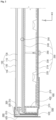
- FIG. 1 is a schematic exploded perspective view of a liquid crystal display device according to an embodiment of the present disclosure.
- FIG. 2 is a schematic cross-sectional view of a liquid crystal display device according to an embodiment of the present disclosure and illustrates a part of the liquid crystal display device according to an embodiment of the present disclosure.
- the liquid crystal display device may include a liquid crystal panel 100, a backlight unit 200, a guide panel 300, a support main 400, a bottom cover 500, and a top cover 600.
- the guide panel 300, the support main 400, the bottom cover 500, and the top cover 600 may be joined to each other by a fastening means such as a screw.
- the liquid crystal panel 100 may include a first substrate 110 at a lower position, a second substrate 120 at an upper position, and a liquid crystal layer interposed between the first and second substrates 110 and 120.
- the first substrate 110 may include a plurality of gate lines and a plurality of data lines on an inner surface thereof, and the gate lines and the data lines may cross each other to define a plurality of pixel regions.
- a thin film transistor, a pixel electrode, and a common electrode may be provided at each pixel region.
- the thin film transistor may be connected to the gate line and the data line, and the pixel electrode may be connected to the thin film transistor.
- the pixel electrode and the common electrode may generate an electric field to drive liquid crystal molecules of the liquid crystal layer.
- This first substrate 110 may be referred to as an array substrate.
- the second substrate 120 may include a black matrix, a color filter layer, and an overcoat layer on an inner surface thereof.
- the black matrix may have openings corresponding to respective pixel regions, and one of red, green, and blue color filters of the color filter layer may include may be disposed to correspond to each opening of the black matrix.
- This second substrate 120 may be referred to as a color filter substrate.
- a first polarizer 130 may be attached to an outer surface of the first substrate 110, that is, a lower surface of the first substrate 110, and the second polarizer 140 may be attached to an outer surface of the second substrate 120, that is, an upper surface of the second substrate 120 in the context of the figures.
- the first polarizer 130 may be disposed under the first substrate 110, and the second polarizer 140 may be disposed over the second substrate 120.
- the first polarizer 130 and the second polarizer 140 may transmit linearly-polarized light only parallel to respective transmission axes.
- the transmission axis of the first polarizer 130 may be perpendicular to the transmission axis of the second polarizer 140.
- the backlight unit 200 may be disposed under the liquid crystal panel 100 to provide light to the liquid crystal panel 100.
- the backlight unit 200 may include a printed circuit board (PCB) 210, a plurality of light emitting diodes LEDs 220, a reflector sheet 230, a diffuser plate 240, and an optical sheet 250.
- PCB printed circuit board
- the backlight unit 200 may be a direct type in which the LEDs 220 of a light source is disposed right under the liquid crystal panel 100.
- Each of the LEDs 220 may be mounted on the printed circuit board 210 in the form of a package including an LED chip and a lens.
- the printed circuit board 210 may supply signals to the LEDs 220.
- the printed circuit board 210 may be provided in plural, and a plurality of LEDs 220 may be mounted on each printed circuit board 210.
- the reflector sheet 230 may be provided over the printed circuit board 210.
- the reflector sheet 230 may have holes corresponding to the LEDs 220, and the LEDs 220 are arranged in the respective holes. Accordingly, the reflector sheet 230 may reflect light from the LEDs 220 toward the liquid crystal panel 100.
- light reflected by the liquid crystal panel 100 or other components over the LEDs 220 and traveling toward the reflector sheet 230 may be reflected by the reflector sheet 230 again and then may be sent back to the liquid crystal panel 100, thereby increasing the light efficiency.
- the reflector sheet 230 may include a plurality of sheet portions, for example, first, second, third, and fourth sheet portions 232, 234, 236, and 238, and this will be described in detail later.
- the diffuser plate 240 may be disposed over the reflector sheet 230.
- the diffuser plate 240 may be spaced apart from the LEDs 220 and the reflector sheet 230 with a predetermined distance and may uniformly diffuse light from the LEDs 220.
- the backlight unit 200 may further include a support member 260 so as to uniformly maintain a space between the LEDs 220 and the diffuser plate 240.
- the support member 260 may have a lower end part penetrating the bottom cover 500 and the printed circuit board 210 and an upper end part contacting a lower surface of the diffuser plate 240, thereby supporting the diffuser plate 240.
- the optical sheet 250 may be disposed over the diffuser plate 240.
- the optical sheet 250 may include at least one diffusion sheet and at least one light-concentrating sheet such that more uniform surface light source can be incident on the liquid crystal panel 100 by diffusing or concentrating the light passing through the diffuser plate 240.
- the optical sheet 250 may include two light-concentrating sheets and one diffusion sheet sequentially disposed over the diffuser plate 240.
- the light-concentrating sheets may include prism patterns or lenticular patterns.
- one of the light-concentrating sheets may include lenticular patterns, and the other may include prism patterns.
- the optical sheet 250 may further include a brightness enhancement film in which layers having different refractive indexes are alternately stacked or may include the brightness enhancement film instead of the diffusion sheet.
- the liquid crystal panel 100 and the backlight unit 200 may be fastened and supported by the guide panel 300, the support main 400, the bottom cover 500, and the top cover 600.
- the liquid crystal panel 100 may be fastened on the guide panel 300.
- the guide panel 300 may be formed along lateral edges of the liquid crystal panel 100, thereby having a planar structure of a substantially square frame shape.
- the guide panel 300 may include a first guide portion 310 and a second guide portion 320.
- the first guide portion 310 may be a horizontal portion extending in an X direction
- the second guide portion 320 may be a vertical portion extending in a Z direction.
- the first guide portion 310 may extend from one side of the second guide portion 320, and a length from a bottom end of the second guide portion 320 to the first guide portion 310 may be longer than a length from a top end of the second guide portion 320 to the first guide portion 310.
- the support main 400 may be disposed under the guide panel 300.
- the support main 400 may have a planar structure of a substantially square frame shape.
- the support main 400 may include a first support portion 410 and a second support portion 420.
- the first support portion 410 may extend in the X direction and may be disposed between the reflector sheet 230 and the bottom cover 500.
- the second support portion 420 may extend from an end of the first support portion 410 and may include at least one vertical part and at least one horizontal part.
- the second support portion 420 may include two vertical parts and one horizontal part therebetween and may have a cross-section of a substantially U-like shape inverted up and down.
- the diffuser plate 240 may be disposed on the second support portion 420. Specifically, an edge of the lower surface of the diffuser plate 240 may be disposed on the horizontal part of the second support portion 420. Accordingly, the diffuser plate 240 and the optical sheet 250 may be disposed between the second support portion 420 and the first guide portion 310, and the second support portion 420 may be in contact with the lower surface of the diffuser plate 240, thereby supporting the diffuser plate 240 and the optical sheet 250.
- the support main 400 may be made of plastic and formed through molding.
- the support main 400 may be formed of white polycarbonate (PC).
- the support main 400 may be formed of metal and may be formed of aluminum (Al), stainless steel (SUS), or electrolytic galvanized iron (EGI), for example.
- the bottom cover 500 may be provided under the support main 400.
- the bottom cover 500 may include a first bottom portion 510 and the second bottom portion 520.
- the first bottom portion 510 may be a horizontal plane and may extend substantially in the X direction.
- the first bottom potion 510 may have at least one bent part to place various components necessary for driving the liquid crystal panel 100, for example, a driving printed circuit board and the like.
- the support main 400 may further include an extension part disposed under the first bottom portion 510 of the bottom cover 500, and the components such as the driving printed circuit board and the like may be disposed between the extension part of the support main 400 and the first bottom portion 510.
- the second bottom portion 520 may be disposed between two vertical parts of the second support portion 420.
- the second bottom portion 520 may be a vertical plane and may extend in the Z direction.
- the second bottom portion 520 may be bended from an edge of the first bottom portion 510.
- the second bottom portion 520 may be disposed between the guide panel 300 and the support main 400, more particularly, between the second guide portion 320 and the second support portion 420.
- the bottom cover 500 may be formed of metal, and may be formed of aluminum (Al) or electrolytic galvanized iron (EGI), for example. However, the present disclosure is not limited thereto, and the bottom cover 500 may be formed of stainless steel (SUS).
- the top cover 600 may be provided over the liquid crystal panel 100.
- the top cover 600 may have a planar structure of a substantially square frame shape.
- the top cover 600 may include a first top portion 610 and a second top portion 620.
- the first top portion 610 may be a horizontal portion extending in an X direction
- the second top portion 620 may be a vertical portion extending in a Z direction.
- the top cover 600 may have a cross-section of a substantially L-like shape inverted up and down.
- the first top portion 610 may cover edges of a front surface of the liquid crystal panel 100 and expose a central portion of the front surface of the liquid crystal panel 100, so that an image implemented by the liquid crystal panel 100 may be displayed to the outside.
- the second top portion 620 may cover outer lateral surfaces of the guide panel 300, more particularly, outer surfaces of the second guide portion 320.
- the top cover 600 may be assembled and combined together with the guide panel 300, the support main 400, and the bottom cover 500, so that the liquid crystal display device of the present disclosure may be modularized. Alternatively, the top cover 600 may be omitted.
- top cover 600 may be referred to as a top frame, case top, or top case
- bottom cover 500 may be referred to as a cover bottom or bottom frame
- guide panel 300 may be referred to as a main frame
- support main 400 may be referred to as a main support.
- the liquid crystal display device may have a relatively large size, and for example, a diagonal length of the device may be more than 50 inches. In this case, it is difficult to manufacture the component of the backlight unit 200 as a single configuration. Specially, it is difficult to form the reflector sheet 230 as a single configuration because the reflector sheet 230 has the plurality of holes corresponding to the plurality of LEDs 220, as described above.
- the reflector sheet 230 may be formed of plastic, for example, polyethylene terephthalate (PET).
- PET polyethylene terephthalate
- the plurality of holes may be formed by simultaneous blanking or punching.
- a certain number of holes for example, 150 or more holes are formed in one sheet, it is difficult to form the reflector sheet 230 at once due to strong blanking or punching pressure.
- the reflector sheet 230 may be divided into the plurality of sheet portions, for example, into the first, second, third, and fourth sheet portions 232, 234, 236, and 238, and the first, second, third, and fourth sheet portions 232, 234, 236, and 238 may be fixed to each other by reflective tapes 700. This will be described with reference to FIG. 3 and FIGS. 4A and 4B .
- FIG. 3 is a schematic plan view of a reflector sheet of a backlight unit according to an embodiment of the present disclosure
- FIGS. 4A and 4B are enlarged plan views schematically illustrating an arrangement of sheet portions in accordance with an assembly order of a reflector sheet of a backlight unit according to an embodiment of the present disclosure.
- the reflector sheet 230 of the backlight unit may include the first, second, third, and fourth sheet portions 232, 234, 236, and 238.
- the first sheet portion 232 and the second sheet portion 234 may be arranged adjacent to each other in the X direction
- the third sheet portion 236 and the fourth sheet portion 238 may be arranged adjacent to each other in the X direction.
- the first sheet portion 232 and the third sheet portion 236 may be arranged adjacent to each other in the Y direction
- the second sheet portion 234 and the fourth sheet portion 238 may be arranged adjacent to each other in the Y direction.
- the first, second, fourth, and third sheet portions 232, 234, 238, and 236 may be sequentially arranged in a clockwise direction.
- the X direction may be defined as a first direction
- the Y direction may be defined as a second direction
- the Y direction may be defined as a first direction
- the X direction may be defined as a second direction.
- Each of the first, second, third, and fourth sheet portions 232, 234, 236, and 238 may include a plurality of first holes 232a, 234a, 236a, and 238a and a plurality of second holes 232b, 234b, 236b, and 238b.
- the first holes 232a, 234a, 236a, and 238a may be LED holes and may correspond to the LEDs 220 of FIG. 2 , respectively. Accordingly, the LEDs 220 of FIG. 2 may be exposed through the corresponding first holes 232a, 234a, 236a, and 238a, respectively.
- the number of the first holes 232a, 234a, 236a, and 238a may be less than 150.
- each of the first, second, third, and fourth sheet portions 232, 234, 236, and 238 may have 144 first holes 232a, 234a, 236a, and 238a.
- the second holes 232b, 234b, 236b, and 238b may be screw holes for combining with the bottom cover 500 of FIG. 2 .
- the number of the second holes 232b, 234b, 236b, and 238b may be smaller than the number of the first holes 232a, 234a, 236a, and 238a.
- the present disclosure is not limited thereto.
- the assembly order of the first, second, third, and fourth sheet portions 232, 234, 236, and 238 may be determined by considering the amount of thermal expansion of the reflector sheet 230 and/or the bottom cover 500 of FIG. 2 .
- the reflector sheet 230 may be formed of plastic such as polyethylene terephthalate (PET), and the bottom cover 500 of FIG. 2 may be formed of metal such as aluminum (Al) or electrolytic galvanized iron (EGI).
- the amount of thermal expansion of the reflector sheet 230 may vary depending on the material of the bottom cover 500 of FIG. 2 .
- first, second, third, and fourth sheet portions 232, 234, 236, and 238 may be assembled in consideration of the amount of thermal expansion of the reflector sheet 230 and/or the bottom cover 500 of FIG. 2 , so that problems may not be caused even if the reflector sheet 230 contracts or expands due to temperature changes.
- the first and fourth sheet portions 232 and 238 may be fixed, while the second and third sheet portions 234 and 236 may be movable.
- first and fourth sheet portions 232 and 238 to be fixed may be first assembled as shown in FIG. 4A and then the second and third sheet portions 234 and 236 to be movable may be assembled as shown in FIG. 4B .
- the assembly order of the first and fourth sheet portions 232 and 238 and the assembly order of the second and third sheet portions 234 and 236 may not be limited.
- the fourth, first, third, and second sheet portions 238, 232, 236, and 234 may be sequentially combined to each other.
- the first, fourth, second, and third sheet portions 232, 238, 234, and 236 may be sequentially combined to each other.
- the second holes 234b and 236b provided in the second and third sheet portions 234 and 236 may are larger than the second holes 232b and 238b provided in the first and fourth sheet portions 232 and 238.
- each of the first, second, third, and fourth sheet portions 232, 234, 236, and 238 may further include third holes corresponding to a plurality of support members 260 of FIG. 2 , respectively.
- the adjacent first, second, third, and fourth sheet portions 232, 234, 236, and 238 may overlap each other and may be fixed by a plurality of reflective tapes 700.
- a total of thirteen reflective tapes 700 may be used.
- two reflective tapes 700 may be used between the first and second sheet portions 232 and 234 adjacent to each other in the X direction, and two reflective tapes 700 may be used between the third and fourth sheet portions 236 and 238 adjacent to each other in the X direction.
- Four reflective tapes 700 may be used between the first and third sheet portions 232 and 236 adjacent to each other in the Y direction, and four reflective tapes 700 may be used between the second and fourth sheet portions 234 and 238 adjacent to each other in the Y direction.
- One reflective tape 700 may be used at a central area where the first, second, third, and fourth sheet portions 232, 234, 236, and 238 are adjacent to each other.
- the present disclosure is not limited thereto, and the number of the reflective tapes 700 may vary.
- Each of the plurality of reflective tapes 700 may have at least one cutout, and the cutout may extend in a length direction of the reflective tape 700. Accordingly, first reflective tapes 700a between the first and second sheet portions 232 and 234 or between the third and fourth sheet portions 236 and 238 adjacent to each other in the X direction may have a cutout extending in the Y direction, and second reflective tapes 700b between the first and third sheet portions 232 and 236 or between the second and fourth sheet portions 234 and 238 adjacent to each other in the Y direction may have a cutout extending in the X direction.
- a third reflective tape 700c at the central area where the first, second, third, and fourth sheet portions 232, 234, 236, and 238 are adjacent to each other may have a cutout extending in the X direction and may further have a cutout extending in the Y direction.
- FIG. 5 is an enlarged plan view schematically illustrating the area A1 of FIG. 3 and shows the LEDs together.
- the second sheet portion 234 and the fourth sheet portion 238 may be arranged adjacent to each other in the Y direction.
- Each of the second sheet portion 234 and the fourth sheet portion 238 may have the plurality of first holes 234a and 238a, and the plurality of LEDs 220 may be disposed in the plurality of first holes 234a and 238a, respectively.
- the plurality of LEDs 220 may be arranged at regular intervals and may be spaced apart from each other with a first pitch p1 and a second pitch p2 in the X direction and the Y direction, respectively.
- each of the first and second pitches p1 and p2 may be 50 mm to 80 mm, beneficially 60 mm to 70 mm, more beneficially 65 mm to 70 mm, but the present disclosure is not limited thereto.
- first pitch p1 may be greater than the second pitch p2.
- first pitch p1 and the second pitch p2 may be the same.
- the second sheet portion 234 may overlap the fourth sheet portion 238 to form an overlapping area OA.
- a width of the overlapping area OA may be determined in consideration of contraction and expansion of the reflector sheet 230 and may be 20 nm to 30 nm, for example. However, the present disclosure is not limited thereto.
- the second sheet portion 234 and the fourth sheet portion 238 may be fixed by the reflective tape 700.
- the reflective tape 700 may overlap and contact the second sheet portion 234 and the fourth sheet portion 238.
- the reflective tape 700 may have a length a1 of the X direction and a width a2 of the Y direction, and the length a1 may be greater than the width a2.
- the length a1 of the reflective tape 700 may be greater than the first pitch p1, and the width a2 may be smaller than the second pitch p2.
- the length a1 of the reflective tape 700 may be 60 mm to 80 mm, and the width a2 may be 20 mm to 30 mm. However, present disclosure is not limited thereto. If the length a1 is greater than 80 mm, the reflective tape 700 may be harder than the reflector sheet 230 of FIG. 3 , so that wrinkles may be formed on the reflector sheet 230 of FIG. 3 .
- the reflective tape 700 may have lower flexibility than the reflector sheet 230 of FIG. 3 .
- the thickness of the reflector sheet 230 of FIG. 3 may be 0.2 mm to 0.3 mm, and the thickness of the reflective tape 700 may be greater than 0.3 mm and smaller than or equal to 0.4 mm.
- the present disclosure is not limited thereto.
- the reflective tape 700 may have a plurality of cutouts 710 extending in the X direction.
- the plurality of cutouts 710 may be provided in at least one row, e.g. in three rows spaced apart in the Y direction, and each row may include two or more cutouts 710 extending and spaced apart in the X direction.
- the present disclosure is not limited thereto, and the number of cutouts 710 may vary.
- the plurality of cutouts 710 may impart flexibility to the reflector tape 700, so that the reflector tape 700 can be prevented from being detached from the second and fourth sheet portions 234 and 238 even if the reflector sheet 230 contracts or expands due to the temperature changes.
- the cutouts 710 may be used as a guide line for an attachment location, so that the reflective tape 700 can be precisely attached to the overlapping area OA of the second and fourth sheet portions 234 and 238. Accordingly, it is possible to prevent detachment of the reflective tape 700 due to incorrect attachment.
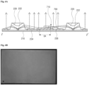
- FIG. 6A is a schematic cross-sectional view of a reflector sheet and a reflective tape according to an embodiment of the present disclosure and illustrates a cross-section corresponding to the line I-I' of FIG. 5
- FIG. 6B is a view showing reliability evaluation results of the reflector sheet and the reflective tape according to an embodiment of the present disclosure
- FIG. 7A is a schematic cross-sectional view of a reflector sheet and a reflective tape according to a comparative example
- FIG. 7B is a view showing reliability evaluation results of the reflector sheet and the reflective tape according to a comparative example.
- the second sheet portion 234 and the fourth sheet portion 238 having the overlapping area OA may be disposed on the printed circuit board 210, and the reflective tape 700 may overlap and contact the second sheet portion 234 and the fourth sheet portion 238 to thereby fix the second and fourth sheet portions 234 and 238.
- the reflective tape 700 may have the plurality of cutouts 710, and some of the plurality of cutouts 710 may correspond to one end of the overlapping area OA.
- the detachment of the reflective tape 700 due to the temperature changes can be prevented by the plurality of cutouts 710, so that light from the LED chip 222 of the LED 220 can be uniformly reflected by the second and fourth sheet portions 234 and 238.
- a reflective tape 7000 according to the comparative example does not include a cutout.
- the reflective tape 7000 is detached from the fourth sheet portion 238, and a separation occurs between the second and fourth sheet portions 234 and 238.
- the reflective tape 700 of the present disclosure will be described in detail with reference to FIGS. 8 to 10 .
- FIG. 8 is a plan view schematically illustrating a reflective tape according to an embodiment of the present disclosure.
- the reflective tape 700 may have a rectangular shape with a length of the X direction and a width of the Y direction and may have a plurality of cutouts 710 extending in the X direction.
- each of the plurality of cutouts 710 may have a first length b1 in the X direction and a second length b2 in the Y direction.
- the first length b1 is greater than the second length b2.
- each of the plurality of cutouts 710 may be spaced apart with a first interval b3 in the X direction and spaced apart with a second interval b4 in the Y direction.
- the first length b1 and the first interval b3 of the plurality of cutouts 710 may have a ratio of about 3: 1, so that the reflective tape 700 may have flexibility against thermal expansion.
- first length b1 and the second interval b4 may be the same. Alternatively, the first length b1 and the second interval b4 may be different.
- the first length b1 may be 4.5 mm to 7 mm
- the second length b2 may be 0.3 mm to 1.3 mm
- the first interval b3 may be 1.6 mm to 2.3 mm
- the second interval b4 may be 5 mm to 6 mm.
- the present disclosure is not limited thereto, and the first and second lengths b1 and b2 and the first and second intervals b3 and b4 may vary according to the size of the reflective tape 700.
- FIG. 8 although it is shown that three cutouts 710 are provided in the Y direction, the present disclosure is not limited thereto.
- FIG. 9 and FIG. 10 are views illustrating cross-sections of a reflective tape according to an embodiment of the present disclosure.
- FIG. 9 is a cross-sectional view corresponding to the line II-II' of FIG. 8
- FIG. 10 is a cross-sectional view corresponding to the line III-III' of FIG. 8 .
- the reflective tape 700 may include first, second, third, fourth, and fifth layers 720, 730, 740, 750, and 760 sequentially stacked.
- the first layer 720 and the third layer 740 may be first and second adhesive layers and may be formed of an acrylic or silicone material.
- the second layer 730 may be a base layer and maintain a structure of the reflective tape 700.
- the second layer 730 may be formed of polyethylene terephthalate (PET).
- the fourth layer 750 may be a reflecting layer and may be formed of stretched polyethylene terephthalate.
- the fifth layer 760 may be a diffusing layer and may be formed by coating a diffusion agent. TiO2, microbeads, or PET beads may be used as the diffusion agent, and a matrix material and the diffusion agent may be dispersed in a solvent and then coated.
- the first, second, and third layers 720, 730, and 740 may constitute a double-sided tape
- the fourth and fifth layers 750 and 760 may constitute a reflection unit. That is, the reflective tape 700 may include a double-sided tape 720, 730, and 740 and a reflection unit 750 and 760, and the double-sided tape 720, 730, and 740 may be disposed between the reflection unit 750 and 760 and the reflector sheet 230 of FIG. 3 .
- the reflection unit 750 and 760 may be attached to the reflector sheet 230 of FIG. 3 to reflect light.
- a thickness of the reflection unit 750 and 760 may be thicker than a thickness of the double-sided tape 720, 730, and 740. More particularly, a thickness of the fourth layer 750, which is a reflecting layer, may be thicker than the thickness of the double-sided tape 720, 730, and 740. Accordingly, the thickness of the fourth layer 750 may be thicker than a thickness of the second layer 730, which is a base layer.
- first and third layers 720 and 740 which are adhesive layers, may have the same thickness, and the thickness of each of the first and third layers 720 and 740 may be smaller than the thickness of the second layer 730.
- a thickness of the fifth layer 760 which is a diffusing layer, may be smaller than the thickness of each of the first, second, third, and fourth layers 720, 730, 740, and 750. Therefore, the thickness of the fifth layer 760 may be smaller than the thickness of each of the first and third layers 720 and 740.
- each of the first and third layers 720 and 740 may be 25 ⁇ m
- the thickness of the second layer 730 may be 50 ⁇ m
- the thickness of the fourth layer 750 may be 225 ⁇ m
- the thickness of the fifth layer 760 may be 20 ⁇ m.
- the present disclosure is not limited thereto.
- the reflective tape 700 may include the plurality of cutouts 710, and the plurality of cutouts 710 may be formed through the first, second, third, fourth, and fifth layers 720, 730, 740, 750, and 760.
- the reflective tape 700 when the reflective tape 700 is attached between the stepped area of the adjacent first, second, third, and fourth sheet portions 232, 234, 236 and 238 of the reflector sheet 230 of FIG. 3 , even if the reflector sheet 230 of FIG. 3 contracts and expands due to the temperature changes, the first, second, third, and fourth sheet portions 232, 234, 236, and 238 of FIG. 3 are not separated or detached because the reflective tape 700 has fluidity.
- the reflective tape 700 of the present disclosure may include cutouts having different configurations according to the joined part.
- FIG. 11 and FIG. 12 are plan views schematically illustrating configurations of reflective tapes according to other embodiments of the present disclosure.
- the reflective tape 700 may include a plurality of cutouts 710.
- the cutouts 710 may include first cutouts 712a extending and spaced apart in the X direction and second cutouts 712b extending and spaced apart in the Y direction.
- the first cutouts 712a may be provided as a single row and may be disposed along the center of the reflective tape 700 in the Y direction.
- the second cutouts 712b may be provided as a single row and may be disposed along the center of the reflective tape 700 in the X direction.
- the reflective tape 700 may include a plurality of cutouts 710.
- the cutouts 710 may include a plurality of first cutouts 714a extending and spaced apart in the X direction and a plurality of second cutouts 714b extending and spaced apart in the Y direction.
- the first cutouts 714a and second cutouts 714b may be provided as a plurality of rows.
- the first cutouts 714a may be provided as three rows
- the second cutouts 714b may be provided as nine rows.
- the present disclosure is not limited thereto.
- the reflective tapes 700 of FIG. 11 and FIG. 12 may be applied to the central area of the reflector sheet 230, that is, may be used as the third reflective tape 700c disposed in the area where the first, second, third, and fourth sheet portions 232, 234, 236, and 238 are adjacent to each other.
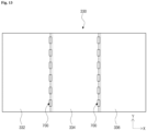
- FIG. 13 is a plan view schematically illustrating another reflector sheet according to an embodiment of the present disclosure.
- the reflector sheet may be divided into three portions.
- another reflector sheet 330 may include first, second, and third sheet portions 332, 334, and 336.
- the first sheet portion 332 and the second sheet portion 334 may be arranged adjacent to each other in the X direction
- the second sheet portion 334 and the third sheet portion 336 may be arranged adjacent to each other in the X direction. Therefore, the second sheet portion 334 may be disposed between the first and third sheet portions 332 and 336.
- each of the first, second, and third sheet portions 332, 334, and 336 may include a plurality of first holes as an LED hole and a plurality of second holes as a screw hole.
- first, second, and third sheet portions 332, 334, and 336 may overlap each other.
- the second sheet portion 334 may be disposed over the first sheet portion 332, and the third sheet portion 336 may be disposed over the second sheet portion 334.
- the adjacent first, second, and third sheet portions 332, 334, and 336 may be fixed by a plurality of reflective tapes 700.
- each of the plurality of reflective tapes 700 may have a plurality of cutouts extending in the Y direction.
- Each of the reflective tapes 700 may have the configuration corresponding to those shown in FIGS. 8 to 12 .
- the number of the divided portions of the reflector sheet of the present disclosure is not limited thereto and may be applied in various ways.
- the reflective tape may have fluidity.
- the reflector tape contracts and expands due to the temperature changes, separation between the adjacent second and fourth sheet portions 234 and 238 can be prevented, and mura can be prevented.
- the reflective tape when the reflective tape is attached, the reflective tape can be precisely attached to the divided reflector sheet using the cutouts, so that it is possible to facilitate work and prevent detachment of the reflective tape 700 due to incorrect attachment.
Landscapes
- Physics & Mathematics (AREA)
- Nonlinear Science (AREA)
- Mathematical Physics (AREA)
- Chemical & Material Sciences (AREA)
- Crystallography & Structural Chemistry (AREA)
- General Physics & Mathematics (AREA)
- Optics & Photonics (AREA)
- Planar Illumination Modules (AREA)
- Liquid Crystal (AREA)
Abstract
Description
- The present application claims the priority of
Korean Patent Application No. 10-2022-0158675 filed on November 23, 2022 - The present disclosure relates to a backlight unit and a display device having the same, and more particularly, to a backlight unit for a liquid crystal display device having a relatively large size and to a liquid crystal display device having the same.
- As the information society is in progress, a demand for display devices that display images increases in various forms, and flat panel display devices (FPD) such as liquid crystal display (LCD) devices and organic light emitting diode (OLED) display devices have been developed and applied to various fields.
- Among the flat panel display devices, liquid crystal display devices have been widely used because of their compact size, light weight, thin thickness, low power driving, and the like.
- The liquid crystal display devices use optical anisotropy and dielectric anisotropy of liquid crystal and include two substrates, a liquid crystal layer between the two substrates, and a pixel electrode and a common electrode for driving liquid crystal molecules of the liquid crystal layer. The liquid crystal display devices control the arrangement of the liquid crystal molecules by an electric field generated by applying a voltage to the pixel electrode and the common electrode and display images by the light transmittance changed accordingly. The liquid crystal display devices have been widely applied to portable devices such as cellphones or multimedia devices, monitors for notebooks or computers, and large televisions.
- Recently, a large-sized liquid crystal display device with a larger area has been required to provide various contents and implement a realistic screen.
- To provide this large-sized liquid crystal display device, the size of the components should increase, and the equipment for manufacturing each component should also increase. However, in the case of a component formed using a mold, it is difficult to produce the component as a single configuration due to the limited size of the mold. Accordingly, some components of the large-sized liquid crystal display device are manufactured by dividing, and various problems may occur in the process of joining and applying the divided portions.
- In particular, when the components of the backlight unit for supplying light are divided and manufactured, it affects the luminance of the liquid crystal display device, and mura occurs at the joined part of the divided portions, resulting in uneven luminance.
- Accordingly, an object of the present disclosure is directed to a backlight unit and a liquid crystal display device having the same that substantially obviate one or more of the problems due to the limitations and disadvantages of the related art.
- More specifically, an object of the present disclosure is to provide a backlight unit for a liquid crystal display device having a relatively large size, and a liquid crystal display device having the same.
- Another object of the present disclosure is directed to a backlight unit and a liquid crystal display device having the same to prevent mura of a large-sized liquid crystal display device.
- At least one of these objects is solved by the features of the independent claim. The features and aspects of the present disclosure are not limited to those described above. Additional features and advantages of the disclosure will be set forth in the description which follows, and in part will be apparent to those skilled in the art from the description or may be learned by practice of the disclosure. These and other advantages of the disclosure may be realized and attained by the structure particularly pointed out in, or derivable from, the written description, claims hereof, and the appended drawings.
- According to one aspect, a liquid crystal display device includes: a bottom cover; a backlight unit disposed over the bottom cover and including a light source and a reflector sheet; and a liquid crystal panel disposed over the backlight unit, wherein the reflector sheet includes first and second sheet portions adjacent to each other in a first direction and at least one first reflective tape fixing the first and second sheet portions, and wherein the at least one first reflective tape includes a plurality of cutouts extending in a second direction perpendicular to the first direction.
- According to a further aspect, a backlight unit, e.g. for a liquid crystal display device, includes: a light source and a reflector sheet; wherein the reflector sheet includes first and second sheet portions adjacent to each other in a first direction and at least one first reflective tape fixing the first and second sheet portions, and wherein the at least one first reflective tape includes a plurality of cutouts extending in a second direction perpendicular to the first direction.
- The backlight unit and/or the liquid crystal display device according to any one of these aspects may include one or more of the following features:
- The first and second sheet portions may overlap each other.
- The plurality of cutouts may be spaced apart from each other in the second direction and/or in the first direction.
- Each of the plurality of cutouts may have a first length of the second direction and a second length of the first direction. The first length may be greater than the second length.
- The plurality of cutouts may be spaced apart with a first interval in the second direction. The first length may be greater than the first interval.
- The plurality of cutouts may be spaced apart with a second interval in the first direction. The second length may be smaller than the second interval.
- The plurality of cutouts may be provided in at least two or in at least three rows spaced apart in the first direction and/or extending in the second direction. Each row may comprise two or more cutouts extending and spaced apart in the second direction.
- The at least one first reflective tape may include a double-sided tape and/or a reflection unit. The double-sided tape may be disposed between the reflection unit and the reflector sheet, i.e. the first sheet portion and second sheet portion of the reflector sheet. A thickness of the reflection unit may be thicker than a thickness of the double-sided tape.
- The reflection unit may include a reflecting layer. A thickness of the reflecting layer may be thicker than a thickness of the double-sided tape. The reflecting layer may be formed of polyethylene terephthalate, in particular of stretched polyethylene terephthalate.
- The reflection unit may further include a diffusing layer. The reflection unit may be disposed between the double-sided tape and the diffusing layer.
- The reflector sheet may further include a third sheet portion adjacent to the first sheet portion in the second direction, and a fourth sheet portion adjacent to the second sheet portion in the second direction. The reflector sheet may further a second reflective tape fixing at least one of the first and third sheet portions and the second and fourth sheet portions.
- The second reflective tape may include a plurality of cutouts extending in the first direction.
- The reflector sheet may further include a third reflective tape fixing the first, second, third, and fourth sheet portions adjacent to each other.
- The third reflective tape may include a plurality of first cutouts extending in the first direction and/or a plurality of second cutouts extending in the second direction.
- The light source may include a plurality of LEDs. The plurality of LEDs may be disposed on a printed circuit board of the backlight unit. The reflector sheet may be disposed on the printed circuit board. The reflector sheet may expose the plurality of LEDs on the printed circuit board through first holes formed therein.
- Each of or at least one of the first, second, third, and fourth sheet portions may have first holes respectively corresponding to the plurality of LEDs. In other words, each of the LEDs may be exposed through one of the first holes of the first, second, third, and fourth sheet portions. Each of or at least one of the first, second, third, and fourth sheet portions may have second holes, e.g. for combining with the bottom cover and/or for mounting the reflector sheet to a bottom cover of a liquid crystal display device and/or for mounting the reflector sheet to the printed circuit board.
- The first and fourth sheet portions may be disposed between the printed circuit board and the second and third sheet portions. The first and fourth sheet portions may be disposed between the bottom cover and the second and third sheet portions.
- The second holes of the second and third sheet portions may be larger than the second holes of the first and fourth sheet portions.
- The backlight unit may further include a printed circuit board on which the light source is mounted. The backlight unit may further include a diffuser plate over the reflector sheet. The backlight unit may further include an optical sheet over the diffuser plate.
- A guide panel may be provided between the backlight unit and the liquid crystal panel.
- A support main may support the diffuser plate and/or the optical sheet. The support main may be disposed under the guide panel.
- The reflector sheet may further include a third sheet portion adjacent to the second sheet portion in the first direction.
- The at least one first reflective tape may fix the second and third sheet portions.
- Adjacent ones of the first, second, and third sheet portions may overlap each other.
- It is to be understood that both the foregoing general description and the following detailed description are explanatory and by way of examples and are intended to provide further explanation of the disclosure as claimed without limiting its scope.
- The accompanying drawings, which are included to provide a further understanding of the disclosure and are incorporated in and constitute a part of this specification, illustrate embodiments of the disclosure and together with the description serve to explain the principles of the disclosure. In the drawings:
-
FIG. 1 is a schematic exploded perspective view of a liquid crystal display device according to an embodiment of the present disclosure; -
FIG. 2 is a schematic cross-sectional view of a liquid crystal display device according to an embodiment of the present disclosure; -
FIG. 3 is a schematic plan view of a reflector sheet of a backlight unit according to an embodiment of the present disclosure; -
FIGS. 4A and 4B are enlarged plan views schematically illustrating an arrangement of sheet portions in accordance with an assembly order of a reflector sheet of a backlight unit according to an embodiment of the present disclosure; -
FIG. 5 is an enlarged plan view schematically illustrating the area A1 ofFIG. 3 ; -
FIG. 6A is a schematic cross-sectional view of a reflector sheet and a reflective tape according to an embodiment of the present disclosure; -
FIG. 6B is a view showing reliability evaluation results of the reflector sheet and the reflective tape according to an embodiment of the present disclosure; -
FIG. 7A is a schematic cross-sectional view of a reflector sheet and a reflective tape according to a comparative example; -
FIG. 7B is a view showing reliability evaluation results of the reflector sheet and the reflective tape according to a comparative example; -
FIG. 8 is a plan view schematically illustrating a reflective tape according to an embodiment of the present disclosure; -
FIG. 9 is a cross-sectional view corresponding to the line II-II' ofFIG. 8 ; -
FIG. 10 is a cross-sectional view corresponding to the line III-III' ofFIG. 8 ; -
FIG. 11 and FIG. 12 are plan views schematically illustrating configurations of reflective tapes according to other embodiments of the present disclosure; and -
FIG. 13 is a plan view schematically illustrating another reflector sheet according to an embodiment of the present disclosure. - Advantages and features of the present disclosure and methods for achieving them will be made clear from embodiments described in detail below with reference to the accompanying drawings. The present disclosure can, however, be implemented in many different forms and should not be construed as being limited to the embodiments set forth herein, and the embodiments are provided such that this disclosure will be thorough and complete and will fully convey the scope of the present disclosure to those skilled in the art to which the present disclosure pertains.
- Shapes, sizes, ratios, angles, numbers, and the like disclosed in the drawings for describing the embodiments of the present disclosure are illustrative, and thus the present disclosure is not limited to the illustrated matters. The same reference numerals refer to the same components throughout this disclosure. Further, in the following description of the present disclosure, when a detailed description of a known related art is determined to unnecessarily obscure the gist of the present disclosure, the detailed description thereof will be omitted herein. When terms such as "including," "having," "consisting of," and the like mentioned in this disclosure are used, other parts can be added unless the term "only" is used herein. When a component is expressed as being singular, being plural is included unless otherwise specified.
- In analyzing a component, an error range is interpreted as being included even when there is no explicit description.
- In describing a positional relationship, for example, when a positional relationship of two parts is described as being "on," "above," "below," "next to," or the like, unless "immediately" or "directly" is used, one or more other parts can be located between the two parts.
- Although the terms first, second, and the like are used to describe various components, these components are not substantially limited by these terms. These terms are used only to distinguish one component from another component. Therefore, a first component described below can substantially be a second component within the technical spirit of the present disclosure.
- Features of various embodiments of the present disclosure can be partially or entirely united or combined with each other, technically various interlocking and driving are possible, and each of the embodiments can be independently implemented with respect to each other or implemented together in a related relationship.
- Reference will now be made in detail to embodiments of the present disclosure, examples of which are illustrated in the accompanying drawings.
-
FIG. 1 is a schematic exploded perspective view of a liquid crystal display device according to an embodiment of the present disclosure.FIG. 2 is a schematic cross-sectional view of a liquid crystal display device according to an embodiment of the present disclosure and illustrates a part of the liquid crystal display device according to an embodiment of the present disclosure. - In
FIG. 1 andFIG. 2 , the liquid crystal display device according to the embodiment of the present disclosure may include aliquid crystal panel 100, abacklight unit 200, aguide panel 300, a support main 400, abottom cover 500, and atop cover 600. Theguide panel 300, the support main 400, thebottom cover 500, and thetop cover 600 may be joined to each other by a fastening means such as a screw. - The
liquid crystal panel 100 may include afirst substrate 110 at a lower position, asecond substrate 120 at an upper position, and a liquid crystal layer interposed between the first andsecond substrates - Although not shown in the figures, the
first substrate 110 may include a plurality of gate lines and a plurality of data lines on an inner surface thereof, and the gate lines and the data lines may cross each other to define a plurality of pixel regions. A thin film transistor, a pixel electrode, and a common electrode may be provided at each pixel region. The thin film transistor may be connected to the gate line and the data line, and the pixel electrode may be connected to the thin film transistor. The pixel electrode and the common electrode may generate an electric field to drive liquid crystal molecules of the liquid crystal layer. Thisfirst substrate 110 may be referred to as an array substrate. - In addition, although not shown in the figures, the
second substrate 120 may include a black matrix, a color filter layer, and an overcoat layer on an inner surface thereof. The black matrix may have openings corresponding to respective pixel regions, and one of red, green, and blue color filters of the color filter layer may include may be disposed to correspond to each opening of the black matrix. Thissecond substrate 120 may be referred to as a color filter substrate. - A
first polarizer 130 may be attached to an outer surface of thefirst substrate 110, that is, a lower surface of thefirst substrate 110, and thesecond polarizer 140 may be attached to an outer surface of thesecond substrate 120, that is, an upper surface of thesecond substrate 120 in the context of the figures. In the figures, thefirst polarizer 130 may be disposed under thefirst substrate 110, and thesecond polarizer 140 may be disposed over thesecond substrate 120. Thefirst polarizer 130 and thesecond polarizer 140 may transmit linearly-polarized light only parallel to respective transmission axes. The transmission axis of thefirst polarizer 130 may be perpendicular to the transmission axis of thesecond polarizer 140. - The
backlight unit 200 may be disposed under theliquid crystal panel 100 to provide light to theliquid crystal panel 100. Thebacklight unit 200 may include a printed circuit board (PCB) 210, a plurality of light emittingdiodes LEDs 220, areflector sheet 230, adiffuser plate 240, and anoptical sheet 250. - The
backlight unit 200 may be a direct type in which theLEDs 220 of a light source is disposed right under theliquid crystal panel 100. - Each of the
LEDs 220 may be mounted on the printedcircuit board 210 in the form of a package including an LED chip and a lens. - The printed
circuit board 210 may supply signals to theLEDs 220. The printedcircuit board 210 may be provided in plural, and a plurality ofLEDs 220 may be mounted on each printedcircuit board 210. - The
reflector sheet 230 may be provided over the printedcircuit board 210. Thereflector sheet 230 may have holes corresponding to theLEDs 220, and theLEDs 220 are arranged in the respective holes. Accordingly, thereflector sheet 230 may reflect light from theLEDs 220 toward theliquid crystal panel 100. In addition, light reflected by theliquid crystal panel 100 or other components over theLEDs 220 and traveling toward thereflector sheet 230 may be reflected by thereflector sheet 230 again and then may be sent back to theliquid crystal panel 100, thereby increasing the light efficiency. - Here, the
reflector sheet 230 may include a plurality of sheet portions, for example, first, second, third, andfourth sheet portions - The
diffuser plate 240 may be disposed over thereflector sheet 230. Thediffuser plate 240 may be spaced apart from theLEDs 220 and thereflector sheet 230 with a predetermined distance and may uniformly diffuse light from theLEDs 220. - In this case, as shown in
FIG. 2 , thebacklight unit 200 may further include asupport member 260 so as to uniformly maintain a space between theLEDs 220 and thediffuser plate 240. Thesupport member 260 may have a lower end part penetrating thebottom cover 500 and the printedcircuit board 210 and an upper end part contacting a lower surface of thediffuser plate 240, thereby supporting thediffuser plate 240. - The
optical sheet 250 may be disposed over thediffuser plate 240. Theoptical sheet 250 may include at least one diffusion sheet and at least one light-concentrating sheet such that more uniform surface light source can be incident on theliquid crystal panel 100 by diffusing or concentrating the light passing through thediffuser plate 240. - For example, the
optical sheet 250 may include two light-concentrating sheets and one diffusion sheet sequentially disposed over thediffuser plate 240. The light-concentrating sheets may include prism patterns or lenticular patterns. In this case, one of the light-concentrating sheets may include lenticular patterns, and the other may include prism patterns. - Meanwhile, the
optical sheet 250 may further include a brightness enhancement film in which layers having different refractive indexes are alternately stacked or may include the brightness enhancement film instead of the diffusion sheet. - The
liquid crystal panel 100 and thebacklight unit 200 may be fastened and supported by theguide panel 300, the support main 400, thebottom cover 500, and thetop cover 600. - First, the
liquid crystal panel 100 may be fastened on theguide panel 300. Theguide panel 300 may be formed along lateral edges of theliquid crystal panel 100, thereby having a planar structure of a substantially square frame shape. - The
guide panel 300 may include afirst guide portion 310 and asecond guide portion 320. Thefirst guide portion 310 may be a horizontal portion extending in an X direction, and thesecond guide portion 320 may be a vertical portion extending in a Z direction. Thefirst guide portion 310 may extend from one side of thesecond guide portion 320, and a length from a bottom end of thesecond guide portion 320 to thefirst guide portion 310 may be longer than a length from a top end of thesecond guide portion 320 to thefirst guide portion 310. - The support main 400 may be disposed under the
guide panel 300. The support main 400 may have a planar structure of a substantially square frame shape. The support main 400 may include afirst support portion 410 and asecond support portion 420. - The
first support portion 410 may extend in the X direction and may be disposed between thereflector sheet 230 and thebottom cover 500. Thesecond support portion 420 may extend from an end of thefirst support portion 410 and may include at least one vertical part and at least one horizontal part. For example, thesecond support portion 420 may include two vertical parts and one horizontal part therebetween and may have a cross-section of a substantially U-like shape inverted up and down. - The
diffuser plate 240 may be disposed on thesecond support portion 420. Specifically, an edge of the lower surface of thediffuser plate 240 may be disposed on the horizontal part of thesecond support portion 420. Accordingly, thediffuser plate 240 and theoptical sheet 250 may be disposed between thesecond support portion 420 and thefirst guide portion 310, and thesecond support portion 420 may be in contact with the lower surface of thediffuser plate 240, thereby supporting thediffuser plate 240 and theoptical sheet 250. - The support main 400 may be made of plastic and formed through molding. For example, the support main 400 may be formed of white polycarbonate (PC). Alternatively, the support main 400 may be formed of metal and may be formed of aluminum (Al), stainless steel (SUS), or electrolytic galvanized iron (EGI), for example.
- The
bottom cover 500 may be provided under the support main 400. Thebottom cover 500 may include afirst bottom portion 510 and thesecond bottom portion 520. Thefirst bottom portion 510 may be a horizontal plane and may extend substantially in the X direction. The firstbottom potion 510 may have at least one bent part to place various components necessary for driving theliquid crystal panel 100, for example, a driving printed circuit board and the like. - Alternatively, the support main 400 may further include an extension part disposed under the
first bottom portion 510 of thebottom cover 500, and the components such as the driving printed circuit board and the like may be disposed between the extension part of the support main 400 and thefirst bottom portion 510. In this case, thesecond bottom portion 520 may be disposed between two vertical parts of thesecond support portion 420. - The
second bottom portion 520 may be a vertical plane and may extend in the Z direction. Thesecond bottom portion 520 may be bended from an edge of thefirst bottom portion 510. Thesecond bottom portion 520 may be disposed between theguide panel 300 and the support main 400, more particularly, between thesecond guide portion 320 and thesecond support portion 420. - The
bottom cover 500 may be formed of metal, and may be formed of aluminum (Al) or electrolytic galvanized iron (EGI), for example. However, the present disclosure is not limited thereto, and thebottom cover 500 may be formed of stainless steel (SUS). - Meanwhile, the
top cover 600 may be provided over theliquid crystal panel 100. Thetop cover 600 may have a planar structure of a substantially square frame shape. Thetop cover 600 may include a firsttop portion 610 and a secondtop portion 620. The firsttop portion 610 may be a horizontal portion extending in an X direction, and the secondtop portion 620 may be a vertical portion extending in a Z direction. Thetop cover 600 may have a cross-section of a substantially L-like shape inverted up and down. - The first
top portion 610 may cover edges of a front surface of theliquid crystal panel 100 and expose a central portion of the front surface of theliquid crystal panel 100, so that an image implemented by theliquid crystal panel 100 may be displayed to the outside. The secondtop portion 620 may cover outer lateral surfaces of theguide panel 300, more particularly, outer surfaces of thesecond guide portion 320. - The
top cover 600 may be assembled and combined together with theguide panel 300, the support main 400, and thebottom cover 500, so that the liquid crystal display device of the present disclosure may be modularized. Alternatively, thetop cover 600 may be omitted. - Here, the
top cover 600 may be referred to as a top frame, case top, or top case, and thebottom cover 500 may be referred to as a cover bottom or bottom frame. In addition, theguide panel 300 may be referred to as a main frame, and the support main 400 may be referred to as a main support. - The liquid crystal display device according to an embodiment of the present disclosure may have a relatively large size, and for example, a diagonal length of the device may be more than 50 inches. In this case, it is difficult to manufacture the component of the
backlight unit 200 as a single configuration. Specially, it is difficult to form thereflector sheet 230 as a single configuration because thereflector sheet 230 has the plurality of holes corresponding to the plurality ofLEDs 220, as described above. - Specifically, the
reflector sheet 230 may be formed of plastic, for example, polyethylene terephthalate (PET). The plurality of holes may be formed by simultaneous blanking or punching. Here, when a certain number of holes, for example, 150 or more holes are formed in one sheet, it is difficult to form thereflector sheet 230 at once due to strong blanking or punching pressure. - Accordingly, the
reflector sheet 230 according to an embodiment of the present disclosure may be divided into the plurality of sheet portions, for example, into the first, second, third, andfourth sheet portions fourth sheet portions reflective tapes 700. This will be described with reference toFIG. 3 andFIGS. 4A and 4B . -
FIG. 3 is a schematic plan view of a reflector sheet of a backlight unit according to an embodiment of the present disclosure, andFIGS. 4A and 4B are enlarged plan views schematically illustrating an arrangement of sheet portions in accordance with an assembly order of a reflector sheet of a backlight unit according to an embodiment of the present disclosure. - In
FIG. 3 andFIGS. 4A and 4B , thereflector sheet 230 of the backlight unit according to an embodiment of the present disclosure may include the first, second, third, andfourth sheet portions first sheet portion 232 and thesecond sheet portion 234 may be arranged adjacent to each other in the X direction, and thethird sheet portion 236 and thefourth sheet portion 238 may be arranged adjacent to each other in the X direction. In addition, thefirst sheet portion 232 and thethird sheet portion 236 may be arranged adjacent to each other in the Y direction, and thesecond sheet portion 234 and thefourth sheet portion 238 may be arranged adjacent to each other in the Y direction. Accordingly, the first, second, fourth, andthird sheet portions - Here, the X direction may be defined as a first direction, and the Y direction may be defined as a second direction. Alternatively, the Y direction may be defined as a first direction, and the X direction may be defined as a second direction.
- Each of the first, second, third, and
fourth sheet portions first holes second holes - The
first holes LEDs 220 ofFIG. 2 , respectively. Accordingly, theLEDs 220 ofFIG. 2 may be exposed through the correspondingfirst holes fourth sheet portions first holes fourth sheet portions first holes - In addition, the
second holes bottom cover 500 ofFIG. 2 . In each of the first, second, third, andfourth sheet portions second holes first holes - The assembly order of the first, second, third, and
fourth sheet portions reflector sheet 230 and/or thebottom cover 500 ofFIG. 2 . As described above, thereflector sheet 230 may be formed of plastic such as polyethylene terephthalate (PET), and thebottom cover 500 ofFIG. 2 may be formed of metal such as aluminum (Al) or electrolytic galvanized iron (EGI). The amount of thermal expansion of thereflector sheet 230 may vary depending on the material of thebottom cover 500 ofFIG. 2 . - Therefore, the first, second, third, and
fourth sheet portions reflector sheet 230 and/or thebottom cover 500 ofFIG. 2 , so that problems may not be caused even if thereflector sheet 230 contracts or expands due to temperature changes. - Here, when the
reflector sheet 230 is combined with thebottom cover 500 ofFIG. 2 , the first andfourth sheet portions third sheet portions - According to this, it is desirable that the first and
fourth sheet portions FIG. 4A and then the second andthird sheet portions FIG. 4B . Here, the assembly order of the first andfourth sheet portions third sheet portions - For example, the fourth, first, third, and
second sheet portions third sheet portions - In order to allow the first and
fourth sheet portions third sheet portions reflector sheet 230 is combined with thebottom cover 500 ofFIG. 2 , thesecond holes third sheet portions second holes fourth sheet portions - Meanwhile, each of the first, second, third, and
fourth sheet portions support members 260 ofFIG. 2 , respectively. - The adjacent first, second, third, and
fourth sheet portions reflective tapes 700. - For example, in the case of the
reflector sheet 230 having a diagonal length of 98 inches, a total of thirteenreflective tapes 700 may be used. Specifically, tworeflective tapes 700 may be used between the first andsecond sheet portions reflective tapes 700 may be used between the third andfourth sheet portions reflective tapes 700 may be used between the first andthird sheet portions reflective tapes 700 may be used between the second andfourth sheet portions reflective tape 700 may be used at a central area where the first, second, third, andfourth sheet portions reflective tapes 700 may vary. - Each of the plurality of
reflective tapes 700 may have at least one cutout, and the cutout may extend in a length direction of thereflective tape 700. Accordingly, firstreflective tapes 700a between the first andsecond sheet portions fourth sheet portions reflective tapes 700b between the first andthird sheet portions fourth sheet portions reflective tape 700c at the central area where the first, second, third, andfourth sheet portions - The configurations of the
reflector sheet 230 and thereflective tape 700 according to an embodiment of the present disclosure will be described with reference toFIG. 5 . -
FIG. 5 is an enlarged plan view schematically illustrating the area A1 ofFIG. 3 and shows the LEDs together. - In
FIG. 5 , thesecond sheet portion 234 and thefourth sheet portion 238 may be arranged adjacent to each other in the Y direction. Each of thesecond sheet portion 234 and thefourth sheet portion 238 may have the plurality offirst holes LEDs 220 may be disposed in the plurality offirst holes - The plurality of
LEDs 220 may be arranged at regular intervals and may be spaced apart from each other with a first pitch p1 and a second pitch p2 in the X direction and the Y direction, respectively. For example, each of the first and second pitches p1 and p2 may be 50 mm to 80 mm, beneficially 60 mm to 70 mm, more beneficially 65 mm to 70 mm, but the present disclosure is not limited thereto. - Here, the first pitch p1 may be greater than the second pitch p2. Alternatively, the first pitch p1 and the second pitch p2 may be the same.
- The
second sheet portion 234 may overlap thefourth sheet portion 238 to form an overlapping area OA. A width of the overlapping area OA may be determined in consideration of contraction and expansion of thereflector sheet 230 and may be 20 nm to 30 nm, for example. However, the present disclosure is not limited thereto. - The
second sheet portion 234 and thefourth sheet portion 238 may be fixed by thereflective tape 700. Thereflective tape 700 may overlap and contact thesecond sheet portion 234 and thefourth sheet portion 238. - The
reflective tape 700 may have a length a1 of the X direction and a width a2 of the Y direction, and the length a1 may be greater than the width a2. Preferably, the length a1 of thereflective tape 700 may be greater than the first pitch p1, and the width a2 may be smaller than the second pitch p2. - For example, the length a1 of the
reflective tape 700 may be 60 mm to 80 mm, and the width a2 may be 20 mm to 30 mm. However, present disclosure is not limited thereto. If the length a1 is greater than 80 mm, thereflective tape 700 may be harder than thereflector sheet 230 ofFIG. 3 , so that wrinkles may be formed on thereflector sheet 230 ofFIG. 3 . - That is, since a thickness of the
reflective tape 700 is thicker than a thickness of thereflector sheet 230 ofFIG. 3 , thereflective tape 700 may have lower flexibility than thereflector sheet 230 ofFIG. 3 . For example, the thickness of thereflector sheet 230 ofFIG. 3 may be 0.2 mm to 0.3 mm, and the thickness of thereflective tape 700 may be greater than 0.3 mm and smaller than or equal to 0.4 mm. However, the present disclosure is not limited thereto. - Meanwhile, the
reflective tape 700 may have a plurality ofcutouts 710 extending in the X direction. The plurality ofcutouts 710 may be provided in at least one row, e.g. in three rows spaced apart in the Y direction, and each row may include two ormore cutouts 710 extending and spaced apart in the X direction. However, the present disclosure is not limited thereto, and the number ofcutouts 710 may vary. - The plurality of
cutouts 710 may impart flexibility to thereflector tape 700, so that thereflector tape 700 can be prevented from being detached from the second andfourth sheet portions reflector sheet 230 contracts or expands due to the temperature changes. - In addition, when the
reflective tape 700 is attached, thecutouts 710 may be used as a guide line for an attachment location, so that thereflective tape 700 can be precisely attached to the overlapping area OA of the second andfourth sheet portions reflective tape 700 due to incorrect attachment. - Therefore, separation between the adjacent second and
fourth sheet portions -
FIG. 6A is a schematic cross-sectional view of a reflector sheet and a reflective tape according to an embodiment of the present disclosure and illustrates a cross-section corresponding to the line I-I' ofFIG. 5 , andFIG. 6B is a view showing reliability evaluation results of the reflector sheet and the reflective tape according to an embodiment of the present disclosure.FIG. 7A is a schematic cross-sectional view of a reflector sheet and a reflective tape according to a comparative example, andFIG. 7B is a view showing reliability evaluation results of the reflector sheet and the reflective tape according to a comparative example. - In
FIG. 6A , thesecond sheet portion 234 and thefourth sheet portion 238 having the overlapping area OA may be disposed on the printedcircuit board 210, and thereflective tape 700 may overlap and contact thesecond sheet portion 234 and thefourth sheet portion 238 to thereby fix the second andfourth sheet portions - Here, the
reflective tape 700 may have the plurality ofcutouts 710, and some of the plurality ofcutouts 710 may correspond to one end of the overlapping area OA. - The detachment of the
reflective tape 700 due to the temperature changes can be prevented by the plurality ofcutouts 710, so that light from theLED chip 222 of theLED 220 can be uniformly reflected by the second andfourth sheet portions - Accordingly, as shown in
FIG. 6B , it can be seen that mura does not occur at the joined part of the divided portions of the reflector sheet. - On the other hand, in
FIG. 7A , areflective tape 7000 according to the comparative example does not include a cutout. In this case, as the second andfourth sheet portions reflective tape 7000 is detached from thefourth sheet portion 238, and a separation occurs between the second andfourth sheet portions - Therefore, light from the
LED chip 222 of theLED 220 is non-uniformly reflected by the second andfourth sheet portions - Accordingly, as shown in
FIG. 7B , it can be seen that mura occurs at the joined part of the divided portions of the reflector sheet. - The
reflective tape 700 of the present disclosure will be described in detail with reference toFIGS. 8 to 10 . -
FIG. 8 is a plan view schematically illustrating a reflective tape according to an embodiment of the present disclosure. - In
FIG. 8 , thereflective tape 700 according to the embodiment of the present disclosure may have a rectangular shape with a length of the X direction and a width of the Y direction and may have a plurality ofcutouts 710 extending in the X direction. - Specifically, each of the plurality of
cutouts 710 may have a first length b1 in the X direction and a second length b2 in the Y direction. The first length b1 is greater than the second length b2. - In addition, each of the plurality of
cutouts 710 may be spaced apart with a first interval b3 in the X direction and spaced apart with a second interval b4 in the Y direction. - Here, the first length b1 and the first interval b3 of the plurality of
cutouts 710 may have a ratio of about 3: 1, so that thereflective tape 700 may have flexibility against thermal expansion. - Further, the first length b1 and the second interval b4 may be the same. Alternatively, the first length b1 and the second interval b4 may be different.
- For example, the first length b1 may be 4.5 mm to 7 mm, the second length b2 may be 0.3 mm to 1.3 mm, the first interval b3 may be 1.6 mm to 2.3 mm, and the second interval b4 may be 5 mm to 6 mm. However, the present disclosure is not limited thereto, and the first and second lengths b1 and b2 and the first and second intervals b3 and b4 may vary according to the size of the
reflective tape 700. - In
FIG. 8 , although it is shown that threecutouts 710 are provided in the Y direction, the present disclosure is not limited thereto. -
FIG. 9 and FIG. 10 are views illustrating cross-sections of a reflective tape according to an embodiment of the present disclosure.FIG. 9 is a cross-sectional view corresponding to the line II-II' ofFIG. 8, and FIG. 10 is a cross-sectional view corresponding to the line III-III' ofFIG. 8 . - In
FIG. 9 and FIG. 10 , thereflective tape 700 may include first, second, third, fourth, andfifth layers - The
first layer 720 and thethird layer 740 may be first and second adhesive layers and may be formed of an acrylic or silicone material. Thesecond layer 730 may be a base layer and maintain a structure of thereflective tape 700. Thesecond layer 730 may be formed of polyethylene terephthalate (PET). - The
fourth layer 750 may be a reflecting layer and may be formed of stretched polyethylene terephthalate. Thefifth layer 760 may be a diffusing layer and may be formed by coating a diffusion agent. TiO2, microbeads, or PET beads may be used as the diffusion agent, and a matrix material and the diffusion agent may be dispersed in a solvent and then coated. - Here, the first, second, and
third layers fifth layers reflective tape 700 may include a double-sided tape reflection unit sided tape reflection unit reflector sheet 230 ofFIG. 3 . - Accordingly, while the
reflector sheet 230 ofFIG. 3 may be fixed through the double-sided tape reflection unit reflector sheet 230 ofFIG. 3 to reflect light. - A thickness of the
reflection unit sided tape fourth layer 750, which is a reflecting layer, may be thicker than the thickness of the double-sided tape fourth layer 750 may be thicker than a thickness of thesecond layer 730, which is a base layer. - In addition, the first and
third layers third layers second layer 730. - Meanwhile, a thickness of the
fifth layer 760, which is a diffusing layer, may be smaller than the thickness of each of the first, second, third, andfourth layers fifth layer 760 may be smaller than the thickness of each of the first andthird layers - For example, the thickness of each of the first and
third layers second layer 730 may be 50 µm, the thickness of thefourth layer 750 may be 225 µm, and the thickness of thefifth layer 760 may be 20 µm. However, the present disclosure is not limited thereto. - As described above, the
reflective tape 700 may include the plurality ofcutouts 710, and the plurality ofcutouts 710 may be formed through the first, second, third, fourth, andfifth layers - Accordingly, when the
reflective tape 700 is attached between the stepped area of the adjacent first, second, third, andfourth sheet portions reflector sheet 230 ofFIG. 3 , even if thereflector sheet 230 ofFIG. 3 contracts and expands due to the temperature changes, the first, second, third, andfourth sheet portions FIG. 3 are not separated or detached because thereflective tape 700 has fluidity. - Therefore, it is possible to prevent light leakage.
- The
reflective tape 700 of the present disclosure may include cutouts having different configurations according to the joined part. -
FIG. 11 and FIG. 12 are plan views schematically illustrating configurations of reflective tapes according to other embodiments of the present disclosure. - In
FIG. 11 , thereflective tape 700 according to another embodiment of the present disclosure may include a plurality ofcutouts 710. Thecutouts 710 may includefirst cutouts 712a extending and spaced apart in the X direction andsecond cutouts 712b extending and spaced apart in the Y direction. - The
first cutouts 712a may be provided as a single row and may be disposed along the center of thereflective tape 700 in the Y direction. Thesecond cutouts 712b may be provided as a single row and may be disposed along the center of thereflective tape 700 in the X direction. - Alternatively, in
FIG. 12 , thereflective tape 700 according to another embodiment of the present disclosure may include a plurality ofcutouts 710. Thecutouts 710 may include a plurality offirst cutouts 714a extending and spaced apart in the X direction and a plurality ofsecond cutouts 714b extending and spaced apart in the Y direction. - The
first cutouts 714a andsecond cutouts 714b may be provided as a plurality of rows. For example, thefirst cutouts 714a may be provided as three rows, and thesecond cutouts 714b may be provided as nine rows. However, the present disclosure is not limited thereto. - The
reflective tapes 700 ofFIG. 11 and FIG. 12 may be applied to the central area of thereflector sheet 230, that is, may be used as the thirdreflective tape 700c disposed in the area where the first, second, third, andfourth sheet portions -
FIG. 13 is a plan view schematically illustrating another reflector sheet according to an embodiment of the present disclosure. Here, the reflector sheet may be divided into three portions. - In
FIG. 13 , anotherreflector sheet 330 according to an embodiment of the present disclosure may include first, second, andthird sheet portions first sheet portion 332 and thesecond sheet portion 334 may be arranged adjacent to each other in the X direction, and thesecond sheet portion 334 and thethird sheet portion 336 may be arranged adjacent to each other in the X direction. Therefore, thesecond sheet portion 334 may be disposed between the first andthird sheet portions - Although not shown in the figure, each of the first, second, and
third sheet portions - Here, adjacent ones of the first, second, and
third sheet portions second sheet portion 334 may be disposed over thefirst sheet portion 332, and thethird sheet portion 336 may be disposed over thesecond sheet portion 334. - The adjacent first, second, and
third sheet portions reflective tapes 700. In this case, each of the plurality ofreflective tapes 700 may have a plurality of cutouts extending in the Y direction. - Each of the
reflective tapes 700 may have the configuration corresponding to those shown inFIGS. 8 to 12 . - In the above embodiments, although the configuration in which the reflector sheet is divided into three or four sheet portions has been described, the number of the divided portions of the reflector sheet of the present disclosure is not limited thereto and may be applied in various ways.
- In the present disclosure, by dividing the reflector sheet, it is possible to provide a backlight unit having a relatively large size and a liquid crystal display device including the same.
- In addition, by fixing the divided reflector sheet using a reflective tape with cutouts, the reflective tape may have fluidity. Thus, when the reflector tape contracts and expands due to the temperature changes, separation between the adjacent second and
fourth sheet portions - Further, when the reflective tape is attached, the reflective tape can be precisely attached to the divided reflector sheet using the cutouts, so that it is possible to facilitate work and prevent detachment of the
reflective tape 700 due to incorrect attachment. - It will be apparent to those skilled in the art that various modifications and variations can be made in the display device of the present disclosure without departing from the technical idea or scope of the disclosure. Thus, it is intended that embodiments of the present disclosure cover the modifications and variations of the disclosure provided they come within the scope of the appended claims and their equivalents.
Claims (15)
- A backlight unit (200), comprising:a light source (220); anda reflector sheet (230) disposed on the light source (220);wherein the reflector sheet (230) includes a first sheet portion (232, 332) and a second sheet portion (234, 334) adjacent to each other in a first direction and at least one first reflective tape (700, 700a) fixing the first and second sheet portions (232, 332, 234, 334) to each other, andwherein the at least one first reflective tape (700, 700a) includes a plurality of cutouts (710) extending in a second direction perpendicular to the first direction.
- The backlight unit (200) of claim 1, wherein each of the plurality of cutouts has a first length (b1) in the second direction and a second length (b2) in the first direction, and the first length (b1) is greater than the second length (b2).
- The backlight unit (200)of claim 2, wherein the cutouts (710) are spaced apart from each other with a first interval (b3) in the second direction, and the first length (b1) is greater than the first interval (b3); and/or
wherein the cutouts (710) are spaced apart from each other with a second interval (b4) in the first direction, and the second length (b2) is smaller than the second interval (b4). - The backlight unit (200) according to any one of the preceding claims, wherein the cutouts (710) are provided in at least two or at least three rows spaced apart from each other in the first direction, and each row comprises two or more cutouts (710) extending and spaced apart from each other in the second direction.
- The backlight unit (200) according to any one of the preceding claims, wherein the at least one first reflective tape (700, 700a) includes a double-sided tape (720, 730, 740) and a reflection unit (750, 760), and the double-sided tape (720, 730, 740) is disposed between the reflection unit (750, 760) and the reflector sheet (230).
- The backlight unit (200) of claim 5, wherein the reflection unit includes a reflecting layer (750), and a thickness of the reflecting layer (750) is thicker than a thickness of the double-sided tape (720, 730, 740).
- The backlight unit (200) of claim 6, wherein the reflecting layer (750) is formed of stretched polyethylene terephthalate.
- The backlight unit (200) of claim 6 or 7, wherein the reflection unit further includes a diffusing layer (760), and the reflecting layer (750) is disposed between the double-sided tape (720, 730, 740) and the diffusing layer (760).
- The backlight unit (200) according to any one of the preceding claims, wherein the reflector sheet (230) further includes a third sheet portion (236) adjacent to the first sheet portion (232) in the second direction and a fourth sheet portion (238) adjacent to the second sheet portion (234) in the second direction,wherein the reflector sheet (230) further includes a second reflective tape (700b) fixing the first and third sheet portions (232, 236) to each other and/or the second and fourth sheet portions (234, 238) to each other, andwherein the second reflective tape (700b) includes a plurality of cutouts (710) extending in the first direction.
- The backlight unit (200) of claim 9, wherein the reflector sheet (230) further includes a third reflective tape (700c) fixing the first, second, third, and fourth sheet portions (232, 234, 236, 238) to each other at a position on the reflector sheet (230) where the first, second, third, and fourth sheet portions (232, 234, 236, 238) are all adjacent to each other, and
wherein the third reflective tape (700c) includes a plurality of first cutouts (712a, 714a) extending in the first direction and a plurality of second cutouts (712b, 714b) extending in the second direction. - The backlight unit (200) of claim 9 or 10, wherein the light source includes a plurality of LEDs (220) on a printed circuit board (210),
wherein each of the first, second, third, and fourth sheet portions (232, 234, 236, 238) has first holes (232a, 234a, 236a, 238a) respectively corresponding to the plurality of LEDs (220) and second holes (232b, 234b, 236b, 238b) for mounting the reflector sheet (230) on the printed circuit board (210) and/or on a bottom cover of a liquid crystal display device. - The backlight unit (200) of claim 11, wherein the first and fourth sheet portions (232, 236) are disposed between the printed circuit board (210) and the second and third sheet portions (234, 238), and
wherein the second holes (234b, 238b) of the second and third sheet portions (234, 238) are larger than the second holes (232b, 236b) of the first and fourth sheet portions (232, 236). - The backlight unit (200) according to any one of the preceding claims, further including:a printed circuit board (210) on which the light source (220) is mounted, the reflector sheet (230) being disposed on the printed circuit board (210);a diffuser plate (240) on the reflector sheet (230); andan optical sheet (250) on the diffuser plate (240).
- A liquid crystal display device, including:a bottom cover (500);a backlight unit (200) according to any one of the preceding claims, the backlight unit (200) being disposed on the bottom cover (500); anda liquid crystal panel (100) on the backlight unit (200).
- The liquid crystal display device of claim 14, further comprising:a guide panel (300) between the backlight unit (200) and the liquid crystal panel (100); and/ora support main (400) disposed under the guide panel (300).
Priority Applications (1)
| Application Number | Priority Date | Filing Date | Title |
|---|---|---|---|
| EP25198758.2A EP4632476A3 (en) | 2022-11-23 | 2023-11-07 | Backlight unit and liquid crystal display device |
Applications Claiming Priority (1)
| Application Number | Priority Date | Filing Date | Title |
|---|---|---|---|
| KR1020220158675A KR20240076277A (en) | 2022-11-23 | 2022-11-23 | Liquid Crystal Display Device |
Related Child Applications (2)
| Application Number | Title | Priority Date | Filing Date |
|---|---|---|---|
| EP25198758.2A Division-Into EP4632476A3 (en) | 2022-11-23 | 2023-11-07 | Backlight unit and liquid crystal display device |
| EP25198758.2A Division EP4632476A3 (en) | 2022-11-23 | 2023-11-07 | Backlight unit and liquid crystal display device |
Publications (2)
| Publication Number | Publication Date |
|---|---|
| EP4375740A1 true EP4375740A1 (en) | 2024-05-29 |
| EP4375740B1 EP4375740B1 (en) | 2025-10-15 |
Family
ID=88731417
Family Applications (2)
| Application Number | Title | Priority Date | Filing Date |
|---|---|---|---|
| EP25198758.2A Pending EP4632476A3 (en) | 2022-11-23 | 2023-11-07 | Backlight unit and liquid crystal display device |
| EP23208136.4A Active EP4375740B1 (en) | 2022-11-23 | 2023-11-07 | Backlight unit and liquid crystal display device |
Family Applications Before (1)
| Application Number | Title | Priority Date | Filing Date |
|---|---|---|---|
| EP25198758.2A Pending EP4632476A3 (en) | 2022-11-23 | 2023-11-07 | Backlight unit and liquid crystal display device |
Country Status (4)
| Country | Link |
|---|---|
| US (2) | US11994772B1 (en) |
| EP (2) | EP4632476A3 (en) |
| KR (1) | KR20240076277A (en) |
| CN (1) | CN118068611A (en) |
Citations (5)
| Publication number | Priority date | Publication date | Assignee | Title |
|---|---|---|---|---|
| US20160091760A1 (en) * | 2014-09-25 | 2016-03-31 | Panasonic Intellectual Property Management Co., Ltd. | Backlight device and liquid crystal display |
| CN211857135U (en) * | 2019-12-04 | 2020-11-03 | 深圳市兆驰股份有限公司 | Direct type reflector plate and direct type backlight source |
| EP3798720A1 (en) * | 2019-09-26 | 2021-03-31 | Funai Electric Co., Ltd. | Lighting device and display device |
| CN113970861A (en) * | 2021-10-22 | 2022-01-25 | 高创(苏州)电子有限公司 | Reflector plate, backlight module and display device |
| KR20220158675A (en) | 2020-03-27 | 2022-12-01 | 주식회사 엘지생활건강 | cosmetic delivery system |
Family Cites Families (3)
| Publication number | Priority date | Publication date | Assignee | Title |
|---|---|---|---|---|
| KR20030038876A (en) | 2001-11-07 | 2003-05-17 | 주식회사 테크자인 | Large scale light panel assembly made by combining a plurality of small size light panels |
| KR101628228B1 (en) * | 2009-09-10 | 2016-06-09 | 삼성디스플레이 주식회사 | Backlight assembly and display device comprising the same |
| KR101204906B1 (en) | 2012-02-03 | 2012-11-26 | (주)비오스 | An adhesive tape for lcd panel |
-
2022
- 2022-11-23 KR KR1020220158675A patent/KR20240076277A/en active Pending
-
2023
- 2023-09-27 US US18/475,449 patent/US11994772B1/en active Active
- 2023-10-09 CN CN202311301241.5A patent/CN118068611A/en active Pending
- 2023-11-07 EP EP25198758.2A patent/EP4632476A3/en active Pending
- 2023-11-07 EP EP23208136.4A patent/EP4375740B1/en active Active
-
2024
- 2024-04-24 US US18/644,563 patent/US12174488B2/en active Active
Patent Citations (5)
| Publication number | Priority date | Publication date | Assignee | Title |
|---|---|---|---|---|
| US20160091760A1 (en) * | 2014-09-25 | 2016-03-31 | Panasonic Intellectual Property Management Co., Ltd. | Backlight device and liquid crystal display |
| EP3798720A1 (en) * | 2019-09-26 | 2021-03-31 | Funai Electric Co., Ltd. | Lighting device and display device |
| CN211857135U (en) * | 2019-12-04 | 2020-11-03 | 深圳市兆驰股份有限公司 | Direct type reflector plate and direct type backlight source |
| KR20220158675A (en) | 2020-03-27 | 2022-12-01 | 주식회사 엘지생활건강 | cosmetic delivery system |
| CN113970861A (en) * | 2021-10-22 | 2022-01-25 | 高创(苏州)电子有限公司 | Reflector plate, backlight module and display device |
Also Published As
| Publication number | Publication date |
|---|---|
| US12174488B2 (en) | 2024-12-24 |
| US11994772B1 (en) | 2024-05-28 |
| US20240168331A1 (en) | 2024-05-23 |
| EP4375740B1 (en) | 2025-10-15 |
| KR20240076277A (en) | 2024-05-30 |
| US20240272478A1 (en) | 2024-08-15 |
| EP4632476A2 (en) | 2025-10-15 |
| CN118068611A (en) | 2024-05-24 |
| EP4632476A3 (en) | 2025-12-17 |
Similar Documents
| Publication | Publication Date | Title |
|---|---|---|
| US10698260B2 (en) | Liquid crystal display (LCD) device | |
| US7708451B2 (en) | Bottom frame for liquid crystal display device, backlight assembly and liquid crystal display device using the same | |
| US7548287B2 (en) | Backlight assembly comprising guide grooves and adhesive tapes formed therein for attaching flexible printed circuit to light guide plate | |
| US7967489B2 (en) | Optical sheet, method of manufacturing the same and display apparatus having the same | |
| EP2434200A1 (en) | Illumination device, display device and television reception device | |
| US9746155B2 (en) | Backlight assembly with a reflective member covering interface between substrate units | |
| US8740445B2 (en) | Backlight assembly and method of assembling a backlight assembly | |
| US20120120324A1 (en) | Lighting device, display device and television receiver | |
| US10698259B2 (en) | Deformed liquid crystal display device | |
| US9239481B2 (en) | Liquid crystal display module and liquid crystal display device having the same | |
| TWI619989B (en) | Optical member and display device having the same | |
| KR102130517B1 (en) | Backlight unit and liquid crystal display device including the same | |
| US20120086885A1 (en) | Lighting device, display device and television receiver | |
| US11187930B2 (en) | Liquid crystal display device | |
| WO2011055635A1 (en) | Base material for light source unit, illumination device, display device, and television receiving device | |
| KR20150073267A (en) | Backlight unit and liquid crystal display device including the same | |
| KR20120052627A (en) | Liquid crystal display | |
| KR102396604B1 (en) | Liquid crystal display device | |
| JP2013118055A (en) | Lighting apparatus, display device and tv receiving apparatus | |
| EP4375740B1 (en) | Backlight unit and liquid crystal display device | |
| KR102078025B1 (en) | Optical sheet and liquid crystal display device having the same | |
| CN116300170B (en) | Display device | |
| KR101719279B1 (en) | Liquid crystal display device | |
| KR20130026074A (en) | Optical sheet, backlight unit having the same and liquid crystal display device | |
| US12235532B2 (en) | Liquid crystal display device |
Legal Events
| Date | Code | Title | Description |
|---|---|---|---|
| PUAI | Public reference made under article 153(3) epc to a published international application that has entered the european phase |
Free format text: ORIGINAL CODE: 0009012 |
|
| STAA | Information on the status of an ep patent application or granted ep patent |
Free format text: STATUS: REQUEST FOR EXAMINATION WAS MADE |
|
| 17P | Request for examination filed |
Effective date: 20231107 |
|
| AK | Designated contracting states |
Kind code of ref document: A1 Designated state(s): AL AT BE BG CH CY CZ DE DK EE ES FI FR GB GR HR HU IE IS IT LI LT LU LV MC ME MK MT NL NO PL PT RO RS SE SI SK SM TR |
|
| RBV | Designated contracting states (corrected) |
Designated state(s): AL AT BE BG CH CY CZ DE DK EE ES FI FR GB GR HR HU IE IS IT LI LT LU LV MC ME MK MT NL NO PL PT RO RS SE SI SK SM TR |
|
| GRAP | Despatch of communication of intention to grant a patent |
Free format text: ORIGINAL CODE: EPIDOSNIGR1 |
|
| STAA | Information on the status of an ep patent application or granted ep patent |
Free format text: STATUS: GRANT OF PATENT IS INTENDED |
|
| INTG | Intention to grant announced |
Effective date: 20250509 |
|
| GRAS | Grant fee paid |
Free format text: ORIGINAL CODE: EPIDOSNIGR3 |
|
| GRAA | (expected) grant |
Free format text: ORIGINAL CODE: 0009210 |
|
| STAA | Information on the status of an ep patent application or granted ep patent |
Free format text: STATUS: THE PATENT HAS BEEN GRANTED |
|
| AK | Designated contracting states |
Kind code of ref document: B1 Designated state(s): AL AT BE BG CH CY CZ DE DK EE ES FI FR GB GR HR HU IE IS IT LI LT LU LV MC ME MK MT NL NO PL PT RO RS SE SI SK SM TR |
|
| REG | Reference to a national code |
Ref country code: GB Ref legal event code: FG4D Ref country code: CH Ref legal event code: F10 Free format text: ST27 STATUS EVENT CODE: U-0-0-F10-F00 (AS PROVIDED BY THE NATIONAL OFFICE) Effective date: 20251015 |
|
| REG | Reference to a national code |
Ref country code: DE Ref legal event code: R096 Ref document number: 602023007512 Country of ref document: DE |
|
| REG | Reference to a national code |
Ref country code: IE Ref legal event code: FG4D |
|
| PGFP | Annual fee paid to national office [announced via postgrant information from national office to epo] |
Ref country code: DE Payment date: 20251208 Year of fee payment: 3 |
|
| PGFP | Annual fee paid to national office [announced via postgrant information from national office to epo] |
Ref country code: AT Payment date: 20260113 Year of fee payment: 3 |
|
| PGFP | Annual fee paid to national office [announced via postgrant information from national office to epo] |
Ref country code: FR Payment date: 20251125 Year of fee payment: 3 |
|
| REG | Reference to a national code |
Ref country code: NL Ref legal event code: MP Effective date: 20251015 |
|
| REG | Reference to a national code |
Ref country code: AT Ref legal event code: MK05 Ref document number: 1847457 Country of ref document: AT Kind code of ref document: T Effective date: 20251015 |
|
| PG25 | Lapsed in a contracting state [announced via postgrant information from national office to epo] |
Ref country code: NL Free format text: LAPSE BECAUSE OF FAILURE TO SUBMIT A TRANSLATION OF THE DESCRIPTION OR TO PAY THE FEE WITHIN THE PRESCRIBED TIME-LIMIT Effective date: 20251015 |
|
| PG25 | Lapsed in a contracting state [announced via postgrant information from national office to epo] |
Ref country code: ES Free format text: LAPSE BECAUSE OF FAILURE TO SUBMIT A TRANSLATION OF THE DESCRIPTION OR TO PAY THE FEE WITHIN THE PRESCRIBED TIME-LIMIT Effective date: 20251015 |
|
| REG | Reference to a national code |
Ref country code: LT Ref legal event code: MG9D |
|
| PG25 | Lapsed in a contracting state [announced via postgrant information from national office to epo] |
Ref country code: NO Free format text: LAPSE BECAUSE OF FAILURE TO SUBMIT A TRANSLATION OF THE DESCRIPTION OR TO PAY THE FEE WITHIN THE PRESCRIBED TIME-LIMIT Effective date: 20260115 |
|
| PG25 | Lapsed in a contracting state [announced via postgrant information from national office to epo] |
Ref country code: AT Free format text: LAPSE BECAUSE OF FAILURE TO SUBMIT A TRANSLATION OF THE DESCRIPTION OR TO PAY THE FEE WITHIN THE PRESCRIBED TIME-LIMIT Effective date: 20251015 Ref country code: FI Free format text: LAPSE BECAUSE OF FAILURE TO SUBMIT A TRANSLATION OF THE DESCRIPTION OR TO PAY THE FEE WITHIN THE PRESCRIBED TIME-LIMIT Effective date: 20251015 Ref country code: HR Free format text: LAPSE BECAUSE OF FAILURE TO SUBMIT A TRANSLATION OF THE DESCRIPTION OR TO PAY THE FEE WITHIN THE PRESCRIBED TIME-LIMIT Effective date: 20251015 |
|
| PG25 | Lapsed in a contracting state [announced via postgrant information from national office to epo] |
Ref country code: RS Free format text: LAPSE BECAUSE OF FAILURE TO SUBMIT A TRANSLATION OF THE DESCRIPTION OR TO PAY THE FEE WITHIN THE PRESCRIBED TIME-LIMIT Effective date: 20260115 |
|
| PG25 | Lapsed in a contracting state [announced via postgrant information from national office to epo] |
Ref country code: IS Free format text: LAPSE BECAUSE OF FAILURE TO SUBMIT A TRANSLATION OF THE DESCRIPTION OR TO PAY THE FEE WITHIN THE PRESCRIBED TIME-LIMIT Effective date: 20260215 |
|
| PG25 | Lapsed in a contracting state [announced via postgrant information from national office to epo] |
Ref country code: PT Free format text: LAPSE BECAUSE OF FAILURE TO SUBMIT A TRANSLATION OF THE DESCRIPTION OR TO PAY THE FEE WITHIN THE PRESCRIBED TIME-LIMIT Effective date: 20260216 |
|
| PG25 | Lapsed in a contracting state [announced via postgrant information from national office to epo] |
Ref country code: PL Free format text: LAPSE BECAUSE OF FAILURE TO SUBMIT A TRANSLATION OF THE DESCRIPTION OR TO PAY THE FEE WITHIN THE PRESCRIBED TIME-LIMIT Effective date: 20251015 |
|
| PG25 | Lapsed in a contracting state [announced via postgrant information from national office to epo] |
Ref country code: LV Free format text: LAPSE BECAUSE OF FAILURE TO SUBMIT A TRANSLATION OF THE DESCRIPTION OR TO PAY THE FEE WITHIN THE PRESCRIBED TIME-LIMIT Effective date: 20251015 |
|
| PG25 | Lapsed in a contracting state [announced via postgrant information from national office to epo] |
Ref country code: BG Free format text: LAPSE BECAUSE OF FAILURE TO SUBMIT A TRANSLATION OF THE DESCRIPTION OR TO PAY THE FEE WITHIN THE PRESCRIBED TIME-LIMIT Effective date: 20251015 |