EP4373124A1 - Optical semiconductor module and sample observation device - Google Patents
Optical semiconductor module and sample observation device Download PDFInfo
- Publication number
- EP4373124A1 EP4373124A1 EP22842157.4A EP22842157A EP4373124A1 EP 4373124 A1 EP4373124 A1 EP 4373124A1 EP 22842157 A EP22842157 A EP 22842157A EP 4373124 A1 EP4373124 A1 EP 4373124A1
- Authority
- EP
- European Patent Office
- Prior art keywords
- optical semiconductor
- semiconductor module
- wiring
- antenna wiring
- external connection
- Prior art date
- Legal status (The legal status is an assumption and is not a legal conclusion. Google has not performed a legal analysis and makes no representation as to the accuracy of the status listed.)
- Withdrawn
Links
- 239000004065 semiconductor Substances 0.000 title claims abstract description 136
- 230000003287 optical effect Effects 0.000 title claims abstract description 114
- 239000000758 substrate Substances 0.000 claims abstract description 40
- 239000011159 matrix material Substances 0.000 claims abstract description 7
- 239000002609 medium Substances 0.000 description 14
- 239000000463 material Substances 0.000 description 13
- 229910052751 metal Inorganic materials 0.000 description 13
- 239000002184 metal Substances 0.000 description 13
- 239000010408 film Substances 0.000 description 11
- VYPSYNLAJGMNEJ-UHFFFAOYSA-N silicon dioxide Inorganic materials O=[Si]=O VYPSYNLAJGMNEJ-UHFFFAOYSA-N 0.000 description 11
- 239000011347 resin Substances 0.000 description 10
- 229920005989 resin Polymers 0.000 description 10
- 229910052814 silicon oxide Inorganic materials 0.000 description 10
- 229910052719 titanium Inorganic materials 0.000 description 9
- 229910052782 aluminium Inorganic materials 0.000 description 8
- 239000004020 conductor Substances 0.000 description 8
- 229910052750 molybdenum Inorganic materials 0.000 description 8
- 238000002161 passivation Methods 0.000 description 8
- 230000003071 parasitic effect Effects 0.000 description 7
- 230000005540 biological transmission Effects 0.000 description 6
- 239000011521 glass Substances 0.000 description 6
- 238000003384 imaging method Methods 0.000 description 6
- 239000004925 Acrylic resin Substances 0.000 description 5
- 229920000178 Acrylic resin Polymers 0.000 description 5
- 229910052581 Si3N4 Inorganic materials 0.000 description 5
- 229910045601 alloy Inorganic materials 0.000 description 5
- 239000000956 alloy Substances 0.000 description 5
- 239000003990 capacitor Substances 0.000 description 5
- 229910052804 chromium Inorganic materials 0.000 description 5
- HQVNEWCFYHHQES-UHFFFAOYSA-N silicon nitride Chemical compound N12[Si]34N5[Si]62N3[Si]51N64 HQVNEWCFYHHQES-UHFFFAOYSA-N 0.000 description 5
- 229910052779 Neodymium Inorganic materials 0.000 description 4
- 229910021417 amorphous silicon Inorganic materials 0.000 description 4
- 150000002739 metals Chemical class 0.000 description 4
- 210000004027 cell Anatomy 0.000 description 3
- 229910052802 copper Inorganic materials 0.000 description 3
- 239000000945 filler Substances 0.000 description 3
- 238000005286 illumination Methods 0.000 description 3
- 239000007769 metal material Substances 0.000 description 3
- 229920001721 polyimide Polymers 0.000 description 3
- 229910052715 tantalum Inorganic materials 0.000 description 3
- 229910052721 tungsten Inorganic materials 0.000 description 3
- 239000004642 Polyimide Substances 0.000 description 2
- 238000005229 chemical vapour deposition Methods 0.000 description 2
- 230000006866 deterioration Effects 0.000 description 2
- 230000006870 function Effects 0.000 description 2
- 238000000034 method Methods 0.000 description 2
- 229910052759 nickel Inorganic materials 0.000 description 2
- 239000004033 plastic Substances 0.000 description 2
- 229920003023 plastic Polymers 0.000 description 2
- 229920005668 polycarbonate resin Polymers 0.000 description 2
- 239000004431 polycarbonate resin Substances 0.000 description 2
- 230000004044 response Effects 0.000 description 2
- 229920002050 silicone resin Polymers 0.000 description 2
- 239000010409 thin film Substances 0.000 description 2
- RYGMFSIKBFXOCR-UHFFFAOYSA-N Copper Chemical compound [Cu] RYGMFSIKBFXOCR-UHFFFAOYSA-N 0.000 description 1
- 239000004952 Polyamide Substances 0.000 description 1
- 230000004075 alteration Effects 0.000 description 1
- 150000001408 amides Chemical class 0.000 description 1
- 210000004102 animal cell Anatomy 0.000 description 1
- 230000001580 bacterial effect Effects 0.000 description 1
- UMIVXZPTRXBADB-UHFFFAOYSA-N benzocyclobutene Chemical compound C1=CC=C2CCC2=C1 UMIVXZPTRXBADB-UHFFFAOYSA-N 0.000 description 1
- 230000015572 biosynthetic process Effects 0.000 description 1
- 239000005388 borosilicate glass Substances 0.000 description 1
- 238000006243 chemical reaction Methods 0.000 description 1
- 238000001514 detection method Methods 0.000 description 1
- 230000005611 electricity Effects 0.000 description 1
- 238000005401 electroluminescence Methods 0.000 description 1
- 230000005674 electromagnetic induction Effects 0.000 description 1
- 239000003822 epoxy resin Substances 0.000 description 1
- 238000005530 etching Methods 0.000 description 1
- 230000004907 flux Effects 0.000 description 1
- 239000001963 growth medium Substances 0.000 description 1
- AMGQUBHHOARCQH-UHFFFAOYSA-N indium;oxotin Chemical compound [In].[Sn]=O AMGQUBHHOARCQH-UHFFFAOYSA-N 0.000 description 1
- 239000011368 organic material Substances 0.000 description 1
- 230000002093 peripheral effect Effects 0.000 description 1
- 229920003229 poly(methyl methacrylate) Polymers 0.000 description 1
- 229920002647 polyamide Polymers 0.000 description 1
- 229920006122 polyamide resin Polymers 0.000 description 1
- 229910021420 polycrystalline silicon Inorganic materials 0.000 description 1
- 229920000647 polyepoxide Polymers 0.000 description 1
- 239000009719 polyimide resin Substances 0.000 description 1
- 239000004926 polymethyl methacrylate Substances 0.000 description 1
- 229920001709 polysilazane Polymers 0.000 description 1
- -1 polysiloxane Polymers 0.000 description 1
- 229920001296 polysiloxane Polymers 0.000 description 1
- 230000008569 process Effects 0.000 description 1
- 239000010453 quartz Substances 0.000 description 1
- 230000004043 responsiveness Effects 0.000 description 1
- 229910000679 solder Inorganic materials 0.000 description 1
- 230000003068 static effect Effects 0.000 description 1
- 239000000126 substance Substances 0.000 description 1
- 239000012780 transparent material Substances 0.000 description 1
- 210000005253 yeast cell Anatomy 0.000 description 1
Images



Classifications
-
- H—ELECTRICITY
- H10—SEMICONDUCTOR DEVICES; ELECTRIC SOLID-STATE DEVICES NOT OTHERWISE PROVIDED FOR
- H10D—INORGANIC ELECTRIC SEMICONDUCTOR DEVICES
- H10D30/00—Field-effect transistors [FET]
- H10D30/60—Insulated-gate field-effect transistors [IGFET]
- H10D30/67—Thin-film transistors [TFT]
-
- H—ELECTRICITY
- H10—SEMICONDUCTOR DEVICES; ELECTRIC SOLID-STATE DEVICES NOT OTHERWISE PROVIDED FOR
- H10F—INORGANIC SEMICONDUCTOR DEVICES SENSITIVE TO INFRARED RADIATION, LIGHT, ELECTROMAGNETIC RADIATION OF SHORTER WAVELENGTH OR CORPUSCULAR RADIATION
- H10F39/00—Integrated devices, or assemblies of multiple devices, comprising at least one element covered by group H10F30/00, e.g. radiation detectors comprising photodiode arrays
- H10F39/80—Constructional details of image sensors
- H10F39/811—Interconnections
-
- H—ELECTRICITY
- H01—ELECTRIC ELEMENTS
- H01Q—ANTENNAS, i.e. RADIO AERIALS
- H01Q1/00—Details of, or arrangements associated with, antennas
- H01Q1/12—Supports; Mounting means
- H01Q1/22—Supports; Mounting means by structural association with other equipment or articles
-
- H—ELECTRICITY
- H10—SEMICONDUCTOR DEVICES; ELECTRIC SOLID-STATE DEVICES NOT OTHERWISE PROVIDED FOR
- H10D—INORGANIC ELECTRIC SEMICONDUCTOR DEVICES
- H10D86/00—Integrated devices formed in or on insulating or conducting substrates, e.g. formed in silicon-on-insulator [SOI] substrates or on stainless steel or glass substrates
- H10D86/40—Integrated devices formed in or on insulating or conducting substrates, e.g. formed in silicon-on-insulator [SOI] substrates or on stainless steel or glass substrates characterised by multiple TFTs
-
- H—ELECTRICITY
- H10—SEMICONDUCTOR DEVICES; ELECTRIC SOLID-STATE DEVICES NOT OTHERWISE PROVIDED FOR
- H10D—INORGANIC ELECTRIC SEMICONDUCTOR DEVICES
- H10D86/00—Integrated devices formed in or on insulating or conducting substrates, e.g. formed in silicon-on-insulator [SOI] substrates or on stainless steel or glass substrates
- H10D86/40—Integrated devices formed in or on insulating or conducting substrates, e.g. formed in silicon-on-insulator [SOI] substrates or on stainless steel or glass substrates characterised by multiple TFTs
- H10D86/60—Integrated devices formed in or on insulating or conducting substrates, e.g. formed in silicon-on-insulator [SOI] substrates or on stainless steel or glass substrates characterised by multiple TFTs wherein the TFTs are in active matrices
-
- H—ELECTRICITY
- H10—SEMICONDUCTOR DEVICES; ELECTRIC SOLID-STATE DEVICES NOT OTHERWISE PROVIDED FOR
- H10F—INORGANIC SEMICONDUCTOR DEVICES SENSITIVE TO INFRARED RADIATION, LIGHT, ELECTROMAGNETIC RADIATION OF SHORTER WAVELENGTH OR CORPUSCULAR RADIATION
- H10F39/00—Integrated devices, or assemblies of multiple devices, comprising at least one element covered by group H10F30/00, e.g. radiation detectors comprising photodiode arrays
- H10F39/10—Integrated devices
- H10F39/12—Image sensors
- H10F39/18—Complementary metal-oxide-semiconductor [CMOS] image sensors; Photodiode array image sensors
Definitions
- the present disclosure relates to an optical semiconductor module and a sample observation apparatus.
- Patent Literature 1 A known optical semiconductor module and a known sample observation apparatus are described in, for example, Patent Literature 1.
- Patent Literature 1 Japanese Unexamined Patent Application Publication No. 2018-78130
- an optical semiconductor module includes a substrate including a first surface, a plurality of pixel units in a matrix on the first surface and each including an optical semiconductor component, a drive circuit on the first surface to provide a power supply voltage to the plurality of pixel units and transmit or receive an image signal to or from the plurality of pixel units, a plurality of external connection terminals on the first surface, a plurality of drive wires on the first surface and connecting the drive circuit and the plurality of external connection terminals, and antenna wiring being looped and surrounding the plurality of pixel units, the drive circuit, the plurality of external connection terminals, and the plurality of drive wires in a plan view.
- the antenna wiring includes two ends connected to the drive circuit.
- a sample observation apparatus includes the above optical semiconductor module, a transparent container to contain a medium including a sample, a light source that emits light toward the transparent container, a slit member that allows passage of scattering light resulting from the light being scattered by the medium, a control board including a radiator that radiates an electromagnetic wave toward the antenna wiring, and a flexible wired circuit board connecting the optical semiconductor module and the control board.
- the optical semiconductor component includes a photodetector. The optical semiconductor module is located between the light source and the slit member to receive the scattering light passing through the slit member.
- Patent Literature 1 describes an imaging device including a solid-state image sensor and antenna wiring surrounding the imaging surface of the solid-state image sensor to at least transmit an image from the solid-state image sensor or receive external electric power.
- Such a known imaging device may include a drive circuit for driving the solid-state image sensor.
- the drive circuit may be positioned inefficiently, increasing the size of the imaging device.
- Such a known imaging device may also be affected greatly by parasitic capacitance between signal wiring connected to the drive circuit and the antenna wiring.
- the solid-state image sensor may operate unstably or transmit images or receive external electric power unstably.
- the optical semiconductor module and the sample observation apparatus may include known components not illustrated in the figures, such as circuit boards, wiring conductors, control ICs, and LSI circuits.
- the optical semiconductor module and the sample observation apparatus may include known components not illustrated in the figures, such as circuit boards, wiring conductors, control ICs, and LSI circuits.
- Each figure referred to below is schematic and is not drawn to scale relative to, for example, the actual positions and dimensional ratios of components of the optical semiconductor module and the sample observation apparatus.
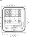
- FIG. 1 is a plan view of an optical semiconductor module according to an embodiment of the present disclosure.
- FIG. 2 is a partially enlarged plan view of the optical semiconductor module according to the embodiment of the present disclosure.
- FIG. 3 is a cross-sectional view taken along line III-III in FIG. 1 .
- FIG. 2 is an enlarged plan view of portion A in FIG. 1 .
- an insulating layer located on a first surface of a substrate and covering multiple pixel units, a drive circuit, multiple drive wires, and antenna wiring is not illustrated.
- an optical semiconductor module 1 includes a substrate 2, multiple pixel units 3, a drive circuit 4, multiple external connection terminals 5, multiple drive wires 6, and antenna wiring 7.
- the substrate 2 includes a first surface (first main surface) 2a, a second surface (second main surface) 2b opposite to the first surface 2a, and third surfaces (side surfaces) 2c connecting the first surface 2a and the second surface 2b.
- the substrate 2 may be, for example, a triangular plate, a rectangular plate including a square plate, a trapezoidal plate, a hexagonal plate, a circular plate, or an elliptic plate, or in any other shape.
- the substrate 2 is made of, for example, a glass material or a resin material.
- the substrate 2 may be transparent.
- the glass material used for the substrate 2 include borosilicate glass, crystallized glass, and quartz.
- the resin material used for the substrate 2 include an epoxy resin, a polyimide resin, a polyamide resin, an acrylic resin, and a polycarbonate resin.
- the pixel units 3 are in a matrix on the first surface 2a of the substrate 2.
- Each pixel unit 3 includes an optical semiconductor component 31.
- the optical semiconductor component 31 may be a light receiver (also referred to as a photodetector) or a light emitter.
- the optical semiconductor component 31 may include both a photodetector and a light emitter.
- the photodetector may include, for example, a photodiode (PD).
- the light emitter may include a self-luminous light emitter such as a light-emitting diode (LED) or a semiconductor laser diode (LD).
- the optical semiconductor component 31 is a photodetector, or more specifically, a photodiode.
- the optical semiconductor module 1 is a photodetection module.
- the multiple pixel units 3 may be hereafter collectively referred to as a photodetection unit B.
- the optical semiconductor module 1 includes multiple gate signal lines GL1 to GLm and multiple read signal lines RL1 to RLn.
- the gate signal lines GL1 to GLm extend in a predetermined first direction (lateral direction in FIG. 1 ).
- the read signal lines RL1 to RLn extend in a second direction (vertical direction in FIG. 1 ) intersecting with the first direction.
- the pixel units 3 are at intersections between the gate signal lines GL1 to GLm and the read signal lines RL1 to RLn.
- the gate signal lines GL1 to GLm may be hereafter collectively referred to as gate signal lines GL without distinguishing the individual gate signal lines.
- the read signal lines RL1 to RLn may be hereafter collectively referred to as read signal lines RL without distinguishing the individual read signal lines.
- Each pixel unit 3 includes a charge storage 32 and a switching element 33 in addition to the photodetector 31, as illustrated in, for example, FIG. 1 .
- the charge storage 32 stores electric charge resulting from photoelectric conversion performed by the photodetector 31.
- the switching element 33 enters a conductive state (on-state) in response to a signal through the corresponding gate signal line GL and outputs a read signal, an electric signal based on the amount of charge in the charge storage 32, to the corresponding read signal line RL.
- the charge storage 32 may include a capacitor.
- the switching element 33 may include a thin-film transistor (TFT).
- the TFT may include a semiconductor film (also referred to as a channel) made of, for example, amorphous silicon (a-Si) or low-temperature polycrystalline silicon (LTPS).
- the TFT may include three terminals that are a gate electrode, a source electrode, and a drain electrode.
- the TFT switches between a conductive state (on-state) and a nonconductive state (off-state) between the source electrode and the drain electrode in response to the voltage applied to the gate electrode.
- the TFT may be an n-channel TFT or a p-channel TFT.
- the switching element 33 may include a CMOS transfer gate. For the switching element 33 including the TFT, the switching element 33 may be referred to as a TFT 33.
- the drive circuit 4 is located on the first surface 2a of the substrate 2.
- the drive circuit 4 may be located on the first surface 2a directly or across an insulating layer 81 made of, for example, silicon oxide (SiO 2 ), silicon nitride (SiNx), or an acrylic resin.
- the insulating layer 81 may include a single insulating layer, or multiple insulating layers stacked on one another.
- the drive circuit 4 includes, for example, a TFT and a wiring conductor.
- the drive circuit 4 can be formed directly on the first surface 2a with a thin film formation method such as chemical vapor deposition (CVD).
- CVD chemical vapor deposition
- the drive circuit 4 supplies electric power to the photodetection unit B and transmits or receives an image signal to or from the photodetection unit B.
- the drive circuit 4 receives a read signal (also referred to as an image signal) from the photodetection unit B.
- the drive circuit 4 may output the received image signal to an external control board (not illustrated).
- the drive circuit 4 includes a gate driver 41 and a selector 42.
- the gate driver 41 is connected to the gate signal lines GL and provides gate voltages to the TFTs 33 in the pixel units 3 through the gate signal lines GL.
- the gate driver 41 provides gate signals to each row of the matrix of the pixel units 3.
- the selector 42 is connected to the read signal lines RL1 to RLn and receives the read signal output from the TFTs 33 in the pixel units 3 through the read signal lines RL.
- the external connection terminals 5 are located on the first surface 2a.
- the external connection terminals 5 may be located on the first surface 2a directly or across the insulating layer 81.
- the external connection terminals 5 are connected (electrically connected) to the electrodes of an external circuit board 13 with a conductive bond such as solder.
- Two intermediate terminals 51 and 52 adjacent to and between the external connection terminals 5 are electrically connected to the antenna wiring 7.
- the intermediate terminals 51 and 52 may be located in the middle of the array of the external connection terminals 5.
- the external connection terminals 5 are connected to an external control board with the external circuit board 13.
- the intermediate terminals 51 and 52 may be covered with the external circuit board 13 for protection.
- the intermediate terminals 51 and 52 are connected to an antenna capacitor that stores electric charge obtained with the antenna wiring 7 or to a processing circuit that processes a received wave component obtained with the antenna wiring 7.
- the external circuit board 13 may transfer image signals obtained by the pixel units 3 to the external control board.
- the external circuit board 13 may transfer a control signal generated by the external control board to the optical semiconductor module 1.
- the external circuit board 13 may be, for example, a flexible printed circuit (FPC) board.
- the antenna capacitor, the processing circuit, or both may be located on the first surface 2a or may be located on the external control board with the external circuit board 13 in between.
- the external connection terminals 5 and the intermediate terminals 51 and 52 are made of a conductive material such as a metal material.
- the external connection terminals 5 and the intermediate terminals 51 and 52 may each include a single metal layer or multiple metal layers stacked on one another.
- the external connection terminals 5 and the intermediate terminals 51 and 52 may be made of, for example, Al, Al/Ti, Ti/Al/Ti, Mo, Mo/Al/Mo, MoNd/AlNd/MoNd, Cu, Cr, Ni, or Ag.
- the stack of Mo/Al/Mo includes a Mo layer, an Al layer, and a Mo layer in this order.
- MoNd is an alloy of Mo and Nd. The same applies to the others.
- the drive wires 6 are located on the first surface 2a and connect the drive circuit 4 and the external connection terminals 5.
- the intermediate terminals 51 and 52 are also connected to the drive circuit 4 with the drive wires 6.
- the drive wires 6 connected to the intermediate terminals 51 and 52 and the drive wires 6 connected to the external connection terminals 5 may be located on the first surface 2a directly or across the insulating layer 81.
- the drive wires 6 are made of a conductive material such as a metal material.
- the drive wires 6 may each include a single metal layer or multiple metal layers stacked on one another.
- the drive wires 6 may be made of, for example, Al, Al/Ti, Ti/Al/Ti, Mo, Mo/Al/Mo, MoNd/AlNd/MoNd, Cu, Cr, Ni, or Ag.
- the antenna wiring 7 is located on the substrate 2. In the present embodiment, the antenna wiring 7 is located on the first surface 2a of the substrate 2. The antenna wiring 7 may be located on the first surface 2a directly or across the insulating layer 81.
- the antenna wiring 7 is looped (or coiled or spiral-shaped).
- the antenna wiring 7 surrounds the photodetection unit B, the drive circuit 4, the external connection terminals 5, and the drive wires 6 in a plan view.
- the antenna wiring 7 includes its two ends 71 and 72 connected to the intermediate terminals 51 and 52.
- the antenna wiring 7 may be connected to the drive circuit 4 without the intermediate terminals 51 and 52.
- the photodetection unit B, the drive circuit 4, the external connection terminals 5, and the drive wires 6 may be hereafter collectively referred to as a surface circuit C.
- the antenna wiring 7 may be looped one or more times along the periphery of the surface circuit C as illustrated in, for example, FIG. 1 .
- the antenna wiring 7 looped multiple times along the periphery of the surface circuit C has a greater wire length, with improved transmission characteristics or reception characteristics.
- the antenna wiring 7 receives external electric power.
- the electric power received by the antenna wiring 7 may be supplied to the drive circuit 4 for driving the pixel units 3.
- the electric power received by the antenna wiring 7 may be used to provide a constant bias voltage to the optical semiconductor components 31 (photodiode) through bias lines 14.
- the power reception with the antenna wiring 7 may be performed through, for example, electromagnetic waves radiated from an external radiator (not illustrated) producing an induced current in the antenna wiring 7 by electromagnetic induction.
- the antenna wiring 7 is made of a conductive material such as a metal material.
- a conductive material such as a metal material.
- the conductive material used for the antenna wiring 7 include a metal such as Al or Cu, and an alloy of these metals.
- the optical semiconductor module 1 includes the antenna wiring 7 surrounding the surface circuit C in a plan view. This structure allows the surface circuit C to be efficiently located in the area surrounded by the antenna wiring 7 on the first surface 2a, reducing the size of the optical semiconductor module 1.
- the optical semiconductor module 1 includes the antenna wiring 7 not overlapping the drive wires 6 in a plan view, with less parasitic capacitance between the antenna wiring 7 and the drive wires 6. This allows the drive circuit 4 and the pixel units 3 to operate stably and the antenna wiring 7 to operate stably.
- the optical semiconductor module 1 may include the antenna wiring 7 overlapping wiring on the external circuit board 13 in a plan view as illustrated in, for example, FIG. 1 .
- the parasitic capacitance between the antenna wiring 7 and the wiring on the external circuit board 13 can be easily reduced by increasing the distance between the antenna wiring 7 and the external circuit board 13 or placing a substance with low capacitance between the antenna wiring 7 and the external circuit board 13.
- the parasitic capacitance between the antenna wiring 7 and the wiring on the external circuit board 13 is less likely to affect the operation of the optical semiconductor module 1.
- the antenna wiring 7 surrounding the surface circuit C can function as a guard ring that reduces static electricity and unintended external electromagnetic waves affecting the surface circuit C (particularly the pixel units 3).
- the optical semiconductor module 1 including the antenna wiring 7 surrounding the surface circuit C can operate stably.
- the antenna wiring 7 includes one or more overlapping areas 73 in which portions of the antenna wiring 7 overlap each other as illustrated in, for example, FIG. 2 .
- the total of the overlapping areas 73 is smaller than the total of overlapping areas in which the antenna wiring 7 overlaps the drive wires 6 when the external connection terminals 5 are located outside the area surrounded by the antenna wiring 7.
- the parasitic capacitance in the overlapping areas 73 is relatively low and is less likely to affect the operation of the optical semiconductor module 1.
- Each overlapping area 73 includes overlapping portions of the antenna wiring 7 across an inorganic insulating film made of, for example, silicon oxide (SiO 2 ) or silicon nitride (SiNx), or a resin insulating film.
- the resin insulating film may be thicker to easily reduce parasitic capacitance affecting the operation.
- the antenna wiring 7 may be located at the periphery of the first surface 2a as illustrated in, for example, FIG. 1 . In this case, the area surrounded by the antenna wiring 7 is larger, easily allowing efficient placement of the surface circuit C.
- the antenna wiring 7 can have a greater wire length with improved transmission characteristics.
- the external connection terminals 5 may be located adj acent to a first side 2aa of the first surface 2a as illustrated in, for example, FIG. 1 .
- This structure facilitates connection between some of the external connection terminals 5 and the electrodes of the external circuit board 13.
- This structure also reduces the likelihood that other wiring (e.g., drive wires 6) between the external connection terminals 5 and the antenna wiring 7 causes parasitic capacitance between the wiring on the external circuit board 13 and the drive wires 6.
- the optical semiconductor module 1 can thus operate stably.
- the antenna wiring 7 may be looped circularly along the periphery of the surface circuit C, independently of the shape of the first surface 2a. This can reduce the electric resistance of the antenna wiring 7 to improve the power reception efficiency of the antenna wiring 7.
- the drive circuit 4 may include a capacitor (not illustrated) that stores electric power supplied from the antenna wiring 7.
- the drive circuit 4 may supply power stored in the capacitor to the pixel units 3 when power reception by the antenna wiring 7 is (temporarily) unstable. This stabilizes the power supply voltage and allows the optical semiconductor module 1 to operate stably.
- the photodetection module 1 may include, on the first surface 2a, an insulating layer 82 covering the photodetection unit B, the drive circuit 4, the drive wires 6, and the antenna wiring 7. This structure reduces the likelihood of the pixel units 3, the drive circuit 4, the drive wires 6, and the antenna wiring 7 separating from the substrate 2, thus improving the reliability of the optical semiconductor module 1.
- the insulating layer 82 may be made of a transparent resin material. Examples of the transparent resin material used for the insulating layer 82 include a fluororesin, a silicone resin, an acrylic resin, a polycarbonate resin, and a polymethyl methacrylate resin.
- the insulating layer 82 may include a single insulating layer, or multiple insulating layers stacked on one another.
- Each external connection terminal 5 may include its peripheral portion partially covered with the insulating layer 82 in a plan view. This reduces the likelihood of the external connection terminals 5 separating from the substrate 2, thus improving the reliability of the optical semiconductor module 1.
- the insulating layer 82 may include a low capacitance portion 82a and a high capacitance portion 82b.
- the low capacitance portion 82a may be between the first side 2aa of the first surface 2a and the external connection terminals 5 in a plan view.
- the low capacitance portion 82a may be made of a resin material having a lower dielectric constant than the resin material used for the high capacitance portion 82b. As illustrated in FIG. 3 , the low capacitance portion 82a may be made of the same material as the high capacitance portion 82b and may be thicker than the high capacitance portion 82b.
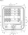
- FIG. 4 is a plan view of the optical semiconductor module according to the embodiment of the present disclosure.
- FIG. 5 is a plan view of the optical semiconductor module according to the embodiment of the present disclosure as viewed in a direction different from the direction in FIG. 4 .
- an optical semiconductor module 1A has the same structure as the optical semiconductor module 1 except for the antenna wiring 7.
- the same reference numerals denote the same or similar components as those of the optical semiconductor module 1, and such components will not be described in detail.
- the antenna wiring 7 includes a portion (also referred to as front wiring) 7a located on the first surface 2a and a portion (also referred to as back wiring) 7b located on the second surface 2b.
- the back wiring 7b may be located on the second surface 2b directly or across an insulating layer made of, for example, silicon oxide (SiO 2 ) or silicon nitride (SiNx).
- the back wiring 7b may extend along the periphery of the second surface 2b.
- the back wiring 7b may be looped at least once along the periphery of the surface circuit C in a plan view. As illustrated in, for example, FIGs.
- the front wiring 7a and the back wiring 7b may be connected with feedthrough conductors 7d extending through the substrate 2 in the thickness direction.
- the front wiring 7a and the back wiring 7b may be connected with side wiring on the third surfaces 2c of the substrate 2.
- the optical semiconductor module 1A can have, without increasing the area of the frame on the first surface 2a, the antenna wiring 7 with a greater length (a greater sum of the length of the front wiring 7a and the length of the back wiring 7b) and thus with improved transmission characteristics, than the antenna wiring 7 including the front wiring 7a alone.
- the optical semiconductor module 1A includes the front wiring 7a looped fewer times along the periphery of the surface circuit C.
- the photodetection module 1 can thus have a narrower frame without reducing the length of the antenna wiring 7. With fewer loops of the front wiring 7a and more loops of the back wiring 7b, the antenna wiring 7 can maintain its length and avoid deterioration in the transmission characteristics.
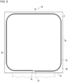
- FIG. 6 is a plan view of the optical semiconductor module according to the embodiment of the present disclosure.
- an optical semiconductor module 1B has the same structure as the optical semiconductor module 1 except for the antenna wiring 7.
- the same reference numerals denote the same or similar components as those of the optical semiconductor module 1, and such components will not be described in detail.
- the antenna wiring 7 includes front wiring 7a located on the first surface 2a and portions (also referred to as side wiring) 7c located on the third surfaces 2c.
- the side wiring 7c may be located on the third surfaces 2c directly or across an insulating layer made of, for example, silicon oxide (SiO 2 ) or silicon nitride (SiNx). As illustrated in, for example, FIG. 6 , the side wiring 7c extends on the third surfaces 2c along the periphery of the substrate 2.
- the side wiring 7c may be looped at least once along the periphery of the substrate 2.
- the optical semiconductor module 1B can have, without increasing the area of the frame on the first surface 2a, the antenna wiring 7 with a greater length (a greater sum of the length of the front wiring 7a and the length of the side wiring 7c) and thus with improved transmission characteristics, than the antenna wiring 7 including the front wiring 7a alone.
- the optical semiconductor module 1B includes the front wiring 7a looped fewer times along the periphery of the surface circuit C.
- the photodetection module 1 can thus have a narrower frame without reducing the length of the antenna wiring 7. With fewer loops of the front wiring 7a and more loops of the side wiring 7c, the antenna wiring 7 can maintain its length and avoid deterioration in the transmission characteristics.
- FIG. 7 is an exploded perspective view of the sample observation apparatus according to the present embodiment.
- FIG. 8 is a cross-sectional view of the sample observation apparatus according to the embodiment of the present disclosure.
- FIG. 9 is a partially enlarged cross-sectional view of the sample observation apparatus according to the embodiment of the present disclosure.
- FIG. 8 schematically illustrates an optical semiconductor module, without illustrating components other than pixel units.
- FIG. 9 is a cross-sectional view of a photodetector and a TFT in a pixel unit, illustrating their structures.
- a sample observation apparatus 100 includes the optical semiconductor module 1, 1A, or 1B, a container 200, a light source 300, a slit member 400, a control board 500, and a flexible printed circuit board 600.
- the optical semiconductor module 1, 1A, or 1B functions as a photodetection module.
- the optical semiconductor component 31 includes a photodetector.
- the optical semiconductor module 1, 1A, or 1B may be hereafter referred to as a photodetection module 1, 1A, or 1B.
- the optical semiconductor component 31 may be referred to as a photodetector 31.
- the photodetector 31 includes a photodiode.
- the photodetector 31 may be a PIN photodiode or a PN photodiode.
- the photodetector 31 is a PIN photodiode.
- the PIN photodiode includes an intrinsic semiconductor layer (i-type semiconductor layer) between a p-n junction.
- the PIN photodiode including the intrinsic semiconductor layer has a larger depletion layer than a PN photodiode when receiving a reverse voltage.
- the PIN photodiode thus has faster responsiveness than a PN photodiode.
- the PIN photodiode has a smaller dark current than a PN photodiode when receiving a reverse voltage.
- Each pixel unit 3 in the photodetection module 1, 1A, or 1B is located on the first surface 2a of the substrate 2 as illustrated in, for example, FIG. 9 .
- the charge storage 32 in the pixel unit 3 is not illustrated.
- the TFT 33 includes a source electrode 33a, a drain electrode 33b, a gate electrode 33c, a semiconductor film (channel) 33d, and a gate insulating film 33e.
- the source electrode 33a and the drain electrode 33b may be made of a metal such as Ta, Nd, W, Ti, Mo, Al, Cr, or Ag, or an alloy of these metals.
- the photodetector 31 may include a passivation layer (not illustrated). The passivation layer may be located on the first surface 2a and cover the TFT 33.
- the photodetector 31 is electrically connected to the drain electrode 33b of the TFT 33 with a lower contact hole 10.
- the photodetector 31 includes a lower electrode layer 31a, a lower extrinsic semiconductor layer 31b, an intrinsic semiconductor layer 31c, an upper extrinsic semiconductor layer 31d, and an upper electrode layer 31e stacked in this order from the substrate 2.
- the lower contact hole 10 may include a part of the lower electrode layer 31a on the inner surface of a recess formed by removing a predetermined portion of the insulating layer 81 by, for example, etching, and an insulating filler 10a filling a space defined by the lower electrode layer 31a.
- the lower electrode layer 31a may be made of a metal such as Ta, Nd, W, Ti, Mo, Al, Cr, or Ag, or an alloy of these metals.
- the lower extrinsic semiconductor layer 3 1b may be made of, for example, n+-type a-Si.
- the intrinsic semiconductor layer 31c may be made of, for example, intrinsic Si (i-type Si).
- the upper extrinsic semiconductor layer 31d may be made of, for example, p+-type a-Si.
- the upper electrode layer 31e may be made of, for example, indium tin oxide (ITO).
- the insulating filler 10a may be made of an organic material such as an acrylic resin, a silicone resin, a polyimide, a polyamide, a polyimide amide, benzocyclobutene, polysiloxane, or polysilazane.
- the photodetector 31 (PIN photodiode) includes the lower electrode layer 31a, the lower extrinsic semiconductor layer 31b, the intrinsic semiconductor layer 31c, the upper extrinsic semiconductor layer 31d, and the upper electrode layer 31e.
- the photodetector 31 photoelectrically converts light entering the intrinsic semiconductor layer 31c through the upper extrinsic semiconductor layer 31d and the upper electrode layer 31e.
- the upper electrode layer 31e is electrically connected to the bias line 14 through an upper contact hole 15.
- the bias line 14 may be made of a metal such as Ta, Nd, W, Ti, Mo, Al, Cr, or Ag, or an alloy of these metals.
- the photodetection module 1, 1A, or 1B may include a first passivation layer 16 and a second passivation layer 17 covering the photodetector 31.
- the first passivation layer 16 and the second passivation layer 17 may be made of, for example, silicon oxide (SiO 2 ), silicon nitride (SiNx), or an acrylic resin.
- the photodetection module 1, 1A, or 1B includes a light-transmissive portion 11 that transmits illumination light L1 emitted from the light source 300 and light-receiving portions 12 that receive scattering light L2 scattered by a medium 800.
- the light-transmissive portion 11 may be between pixel units 3 adjacent to each other.
- the light-receiving portions 12 may be at the pixel units 3 each including the photodetector 31.
- the container 200 contains the medium 800 including samples 700.
- the container 200 is made of an optically transparent material, such as a plastic material or a glass material, to be observable from outside.
- the container 200 may have any shape and size. As illustrated in, for example, FIG. 7 , the container 200 may include a lid 201.
- the container 200 may include multiple container portions for containing the samples 700 and the medium 800.
- the container 200 may or may not have a bottom. When the container 200 has no bottom, the container 200 may be in close contact with the slit member 400 to hold the medium 800.
- the samples 700 include animal cells, plant cells, yeast cells, and bacterial cells.
- the medium 800 may be a culture medium.
- the light source 300 emits illumination light L1 toward the medium 800 contained in the container 200.
- the light source 300 may include, for example, an LED, an LD, an organic electroluminescence (OEL) element, or a cold-cathode fluorescence lamp (CCFL).
- the light source 300 may be a surface emitter including light emitters such as LEDs, LDs, and OEL elements in a matrix.
- the light source 300 may include a diffuser plate or a light guide plate.
- the light source 300 may be an end-face emitter including at least one light source element on an end face of a light guide plate.
- the slit member 400 includes a slit 401 and light shields 402.
- a part of illumination light L1 emitted from the light source 300 is transmitted through the light-transmissive portion 11 in the optical semiconductor module 1, 1A, or 1B, and is scattered by the medium 800 contained in the container 200.
- the scattering light L2 scattered by the medium 800 includes vertical scattering light VL2 perpendicular to the horizontal plane.
- a part of the vertical scattering light VL2 passes through the slit 401 in the slit member 400 and is received by the light-receiving portions 12 in the optical semiconductor module 1, 1A, or 1B.
- the vertical scattering light VL2 can be scattered by the samples 700.
- the amount of light received by the light-receiving portions 12 differs between when the samples 700 are above the slit 401 and when no sample 700 is at a position corresponding to the slit 401.
- the intensity of the vertical scattering light VL2 scattered by the samples 700 can be detected based on the amount of light received by the light-receiving portions 12. This allows detection of any sample 700 above the slit 401.
- the light shields 402 in the slit member 400 reduce the likelihood that light other than the light perpendicular to the horizontal plane scattered by the samples 700 and the medium 800 passes through the slit 401 and is received by the light-receiving portions 12.
- the light shields 402 may be made of a light-shielding material on a surface of a transparent substrate such as a glass substrate or a plastic substrate.
- Each light shield 402 may include a first light shield and a second light shield.
- the first light shield and the second light shield may be spaced from each other in the thickness direction of the substrate 2 (vertical direction in FIG. 8 ).
- the first light shield and the second light shield may have substantially the same shape.
- the first light shield and the second light shield may be located substantially at the same position in a plan view.
- the light shield 402 including the first light shield and the second light shield reduces the likelihood that the scattering light L2 other than the vertical scattering light VL2 passes through the slit member 400 and is received by the light-receiving portions 12.
- the control board 500 includes a radiator 501.
- the radiator 501 radiates electromagnetic waves toward the antenna wiring 7 in the photodetection module 1, 1A, or 1B.
- the radiator 501 may include a looped wire similarly to or in the same manner as the antenna wiring 7.
- the radiator 501 may produce a temporally-variable magnetic flux in an area surrounded by the antenna wiring 7.
- the control board 500 transmits data about the amount of the samples 700 obtained by the photodetection module 1, 1A, or 1B to a monitor 900.
- the control board 500 and the monitor 900 may be connected either with a wire or wirelessly.
- the control board 500 may include a rechargeable battery, a charging control integrated circuit, an impedance matching circuit, an RF reader integrated circuit, a microcomputer, a nonvolatile memory, and a control integrated circuit.
- the monitor 900 receives data transmitted from the control board 500.
- the monitor 902 may include a control integrated circuit, a microcomputer, and a field-programmable gate array (FPGA).
- FPGA field-programmable gate array
- the monitor 900 may be connected to a computer system 901 and transmit the received data to the computer system 901.
- the computer system 901 may include a display to display the received data.
- the flexible printed circuit board 600 electrically connects some of the external connection terminals 5 in the photodetection module 1, 1A, or 1B to the control board 500.
- the flexible printed circuit board 600 may be a known flexible printed circuit board including an insulating and flexible base film to which a conductive metal such as Cu foil is attached to form an electric circuit.
- the sample observation apparatus 100 including the photodetection module 1, 1A, or 1B allows accurate observation of the samples 700.
- optical semiconductor module may be implemented in forms (1) to (10) described below.
- optical semiconductor module and the sample observation apparatus have been described in detail, the optical semiconductor module and the sample observation apparatus according to one or more embodiments of the present disclosure are not limited to the embodiments described above, and may be changed or varied in various manners without departing from the spirit and scope of the present disclosure.
- the components described in the above embodiments may be entirely or partially combined as appropriate unless any contradiction arises.
- the optical semiconductor module 1, 1A, or 1B may include the optical semiconductor component 31 that is a light emitter.
- the optical semiconductor module 1, 1A, or 1B can be a light-emitting module with less display non-uniformity.
- Each pixel unit 3 in the optical semiconductor module 1, 1A, or 1B may include, in addition to the optical semiconductor component 31, at least one selected from the group consisting of a pH sensor, a temperature sensor, an electrical resistance sensor, a pressure sensor, a magnetic sensor, a humidity sensor, a chromaticity sensor, and an illuminance sensor.
- the optical semiconductor module includes the efficiently located drive circuit and can be smaller. In one or more embodiments of the present disclosure, the optical semiconductor module includes the pixel units and the antenna wiring that can operate stably.
- the sample observation apparatus includes the above optical semiconductor module and thus allows accurate observation of samples.
Landscapes
- Solid State Image Pick-Up Elements (AREA)
Abstract
Description
- The present disclosure relates to an optical semiconductor module and a sample observation apparatus.
- A known optical semiconductor module and a known sample observation apparatus are described in, for example,
Patent Literature 1. - Patent Literature 1:
Japanese Unexamined Patent Application Publication No. 2018-78130 - In an aspect of the present disclosure, an optical semiconductor module includes a substrate including a first surface, a plurality of pixel units in a matrix on the first surface and each including an optical semiconductor component, a drive circuit on the first surface to provide a power supply voltage to the plurality of pixel units and transmit or receive an image signal to or from the plurality of pixel units, a plurality of external connection terminals on the first surface, a plurality of drive wires on the first surface and connecting the drive circuit and the plurality of external connection terminals, and antenna wiring being looped and surrounding the plurality of pixel units, the drive circuit, the plurality of external connection terminals, and the plurality of drive wires in a plan view. The antenna wiring includes two ends connected to the drive circuit.
- In an aspect of the present disclosure, a sample observation apparatus includes the above optical semiconductor module, a transparent container to contain a medium including a sample, a light source that emits light toward the transparent container, a slit member that allows passage of scattering light resulting from the light being scattered by the medium, a control board including a radiator that radiates an electromagnetic wave toward the antenna wiring, and a flexible wired circuit board connecting the optical semiconductor module and the control board. The optical semiconductor component includes a photodetector. The optical semiconductor module is located between the light source and the slit member to receive the scattering light passing through the slit member.
- The objects, features, and advantages of the present disclosure will become more apparent from the following detailed description and the drawings.
-
FIG. 1 is a plan view of an optical semiconductor module according to an embodiment of the present disclosure. -
FIG. 2 is a partially enlarged plan view of the optical semiconductor module according to the embodiment of the present disclosure. -
FIG. 3 is a cross-sectional view taken along line III-III inFIG. 1 . -
FIG. 4 is a plan view of an optical semiconductor module according to another embodiment of the present disclosure. -
FIG. 5 is a plan view of the optical semiconductor module according to the other embodiment of the present disclosure as viewed in a direction different from the direction in FIG. 4A. -
FIG. 6 is a plan view of an optical semiconductor module according to still another embodiment of the present disclosure. -
FIG. 7 is an exploded perspective view of a sample observation apparatus according to an embodiment of the present disclosure. -
FIG. 8 is a cross-sectional view of the sample observation apparatus according to the embodiment of the present disclosure. -
FIG. 9 is a partially enlarged cross-sectional view of the sample observation apparatus according to the embodiment of the present disclosure. - An optical semiconductor module and a sample observation apparatus with the structures that form the basis of an optical semiconductor module and a sample observation apparatus according to one or more embodiments of the present disclosure will first be described.
- Various imaging devices have been developed for use in sample observation apparatuses for observing samples such as specimens. For example,
Patent Literature 1 describes an imaging device including a solid-state image sensor and antenna wiring surrounding the imaging surface of the solid-state image sensor to at least transmit an image from the solid-state image sensor or receive external electric power. - Such a known imaging device may include a drive circuit for driving the solid-state image sensor. To avoid overlapping with the antenna wiring, the drive circuit may be positioned inefficiently, increasing the size of the imaging device. Such a known imaging device may also be affected greatly by parasitic capacitance between signal wiring connected to the drive circuit and the antenna wiring. The solid-state image sensor may operate unstably or transmit images or receive external electric power unstably.
- The optical semiconductor module and the sample observation apparatus according to one or more embodiments of the present disclosure will now be described with reference to the accompanying drawings. Each figure referred to below illustrates main components and other elements of the optical semiconductor module and the sample observation apparatus according to one or more embodiments of the present disclosure. In one or more embodiments of the present disclosure, the optical semiconductor module and the sample observation apparatus may include known components not illustrated in the figures, such as circuit boards, wiring conductors, control ICs, and LSI circuits. Each figure referred to below is schematic and is not drawn to scale relative to, for example, the actual positions and dimensional ratios of components of the optical semiconductor module and the sample observation apparatus.
-
FIG. 1 is a plan view of an optical semiconductor module according to an embodiment of the present disclosure.FIG. 2 is a partially enlarged plan view of the optical semiconductor module according to the embodiment of the present disclosure.FIG. 3 is a cross-sectional view taken along line III-III inFIG. 1 .FIG. 2 is an enlarged plan view of portion A inFIG. 1 . InFIGs. 1 and2 , an insulating layer located on a first surface of a substrate and covering multiple pixel units, a drive circuit, multiple drive wires, and antenna wiring is not illustrated. - In the present embodiment, an
optical semiconductor module 1 includes asubstrate 2,multiple pixel units 3, adrive circuit 4, multipleexternal connection terminals 5,multiple drive wires 6, andantenna wiring 7. - The
substrate 2 includes a first surface (first main surface) 2a, a second surface (second main surface) 2b opposite to thefirst surface 2a, and third surfaces (side surfaces) 2c connecting thefirst surface 2a and thesecond surface 2b. Thesubstrate 2 may be, for example, a triangular plate, a rectangular plate including a square plate, a trapezoidal plate, a hexagonal plate, a circular plate, or an elliptic plate, or in any other shape. - The
substrate 2 is made of, for example, a glass material or a resin material. Thesubstrate 2 may be transparent. Examples of the glass material used for thesubstrate 2 include borosilicate glass, crystallized glass, and quartz. Examples of the resin material used for thesubstrate 2 include an epoxy resin, a polyimide resin, a polyamide resin, an acrylic resin, and a polycarbonate resin. - As illustrated in, for example,
FIG. 1 , thepixel units 3 are in a matrix on thefirst surface 2a of thesubstrate 2. Eachpixel unit 3 includes anoptical semiconductor component 31. Theoptical semiconductor component 31 may be a light receiver (also referred to as a photodetector) or a light emitter. Theoptical semiconductor component 31 may include both a photodetector and a light emitter. - The photodetector may include, for example, a photodiode (PD). The light emitter may include a self-luminous light emitter such as a light-emitting diode (LED) or a semiconductor laser diode (LD). In the example described below, the
optical semiconductor component 31 is a photodetector, or more specifically, a photodiode. In other words, theoptical semiconductor module 1 is a photodetection module. Themultiple pixel units 3 may be hereafter collectively referred to as a photodetection unit B. - The
optical semiconductor module 1 includes multiple gate signal lines GL1 to GLm and multiple read signal lines RL1 to RLn. The gate signal lines GL1 to GLm extend in a predetermined first direction (lateral direction inFIG. 1 ). The read signal lines RL1 to RLn extend in a second direction (vertical direction inFIG. 1 ) intersecting with the first direction. Thepixel units 3 are at intersections between the gate signal lines GL1 to GLm and the read signal lines RL1 to RLn. The gate signal lines GL1 to GLm may be hereafter collectively referred to as gate signal lines GL without distinguishing the individual gate signal lines. The read signal lines RL1 to RLn may be hereafter collectively referred to as read signal lines RL without distinguishing the individual read signal lines. - Each
pixel unit 3 includes acharge storage 32 and aswitching element 33 in addition to thephotodetector 31, as illustrated in, for example,FIG. 1 . Thecharge storage 32 stores electric charge resulting from photoelectric conversion performed by thephotodetector 31. The switchingelement 33 enters a conductive state (on-state) in response to a signal through the corresponding gate signal line GL and outputs a read signal, an electric signal based on the amount of charge in thecharge storage 32, to the corresponding read signal line RL. - The
charge storage 32 may include a capacitor. The switchingelement 33 may include a thin-film transistor (TFT). The TFT may include a semiconductor film (also referred to as a channel) made of, for example, amorphous silicon (a-Si) or low-temperature polycrystalline silicon (LTPS). The TFT may include three terminals that are a gate electrode, a source electrode, and a drain electrode. The TFT switches between a conductive state (on-state) and a nonconductive state (off-state) between the source electrode and the drain electrode in response to the voltage applied to the gate electrode. The TFT may be an n-channel TFT or a p-channel TFT. The switchingelement 33 may include a CMOS transfer gate. For the switchingelement 33 including the TFT, the switchingelement 33 may be referred to as aTFT 33. - The
drive circuit 4 is located on thefirst surface 2a of thesubstrate 2. Thedrive circuit 4 may be located on thefirst surface 2a directly or across an insulatinglayer 81 made of, for example, silicon oxide (SiO2), silicon nitride (SiNx), or an acrylic resin. The insulatinglayer 81 may include a single insulating layer, or multiple insulating layers stacked on one another. - The
drive circuit 4 includes, for example, a TFT and a wiring conductor. When thesubstrate 2 is made of a glass material and the TFT in thedrive circuit 4 includes a semiconductor film made of LTPS, thedrive circuit 4 can be formed directly on thefirst surface 2a with a thin film formation method such as chemical vapor deposition (CVD). - The
drive circuit 4 supplies electric power to the photodetection unit B and transmits or receives an image signal to or from the photodetection unit B. For theoptical semiconductor module 1 being a photodetection module, thedrive circuit 4 receives a read signal (also referred to as an image signal) from the photodetection unit B. Thedrive circuit 4 may output the received image signal to an external control board (not illustrated). - The
drive circuit 4 includes agate driver 41 and aselector 42. Thegate driver 41 is connected to the gate signal lines GL and provides gate voltages to theTFTs 33 in thepixel units 3 through the gate signal lines GL. Thegate driver 41 provides gate signals to each row of the matrix of thepixel units 3. Theselector 42 is connected to the read signal lines RL1 to RLn and receives the read signal output from theTFTs 33 in thepixel units 3 through the read signal lines RL. - The
external connection terminals 5 are located on thefirst surface 2a. Theexternal connection terminals 5 may be located on thefirst surface 2a directly or across the insulatinglayer 81. Theexternal connection terminals 5 are connected (electrically connected) to the electrodes of anexternal circuit board 13 with a conductive bond such as solder. Twointermediate terminals external connection terminals 5 are electrically connected to theantenna wiring 7. Theintermediate terminals external connection terminals 5. Theexternal connection terminals 5 are connected to an external control board with theexternal circuit board 13. Theintermediate terminals external circuit board 13 for protection. Theintermediate terminals antenna wiring 7 or to a processing circuit that processes a received wave component obtained with theantenna wiring 7. Theexternal circuit board 13 may transfer image signals obtained by thepixel units 3 to the external control board. Theexternal circuit board 13 may transfer a control signal generated by the external control board to theoptical semiconductor module 1. Theexternal circuit board 13 may be, for example, a flexible printed circuit (FPC) board. The antenna capacitor, the processing circuit, or both may be located on thefirst surface 2a or may be located on the external control board with theexternal circuit board 13 in between. - The
external connection terminals 5 and theintermediate terminals external connection terminals 5 and theintermediate terminals external connection terminals 5 and theintermediate terminals - The
drive wires 6 are located on thefirst surface 2a and connect thedrive circuit 4 and theexternal connection terminals 5. Theintermediate terminals drive circuit 4 with thedrive wires 6. Thedrive wires 6 connected to theintermediate terminals drive wires 6 connected to theexternal connection terminals 5 may be located on thefirst surface 2a directly or across the insulatinglayer 81. - The
drive wires 6 are made of a conductive material such as a metal material. Thedrive wires 6 may each include a single metal layer or multiple metal layers stacked on one another. Thedrive wires 6 may be made of, for example, Al, Al/Ti, Ti/Al/Ti, Mo, Mo/Al/Mo, MoNd/AlNd/MoNd, Cu, Cr, Ni, or Ag. - The
antenna wiring 7 is located on thesubstrate 2. In the present embodiment, theantenna wiring 7 is located on thefirst surface 2a of thesubstrate 2. Theantenna wiring 7 may be located on thefirst surface 2a directly or across the insulatinglayer 81. - As illustrated in, for example,
FIG. 1 , theantenna wiring 7 is looped (or coiled or spiral-shaped). Theantenna wiring 7 surrounds the photodetection unit B, thedrive circuit 4, theexternal connection terminals 5, and thedrive wires 6 in a plan view. As illustrated in, for example,FIG. 2 , theantenna wiring 7 includes its two ends 71 and 72 connected to theintermediate terminals antenna wiring 7 may be connected to thedrive circuit 4 without theintermediate terminals drive circuit 4, theexternal connection terminals 5, and thedrive wires 6 may be hereafter collectively referred to as a surface circuit C. - In a plan view, the
antenna wiring 7 may be looped one or more times along the periphery of the surface circuit C as illustrated in, for example,FIG. 1 . Theantenna wiring 7 looped multiple times along the periphery of the surface circuit C has a greater wire length, with improved transmission characteristics or reception characteristics. In the present embodiment, theantenna wiring 7 receives external electric power. The electric power received by theantenna wiring 7 may be supplied to thedrive circuit 4 for driving thepixel units 3. The electric power received by theantenna wiring 7 may be used to provide a constant bias voltage to the optical semiconductor components 31 (photodiode) through bias lines 14. The power reception with theantenna wiring 7 may be performed through, for example, electromagnetic waves radiated from an external radiator (not illustrated) producing an induced current in theantenna wiring 7 by electromagnetic induction. - The
antenna wiring 7 is made of a conductive material such as a metal material. Examples of the conductive material used for theantenna wiring 7 include a metal such as Al or Cu, and an alloy of these metals. - In the present embodiment, the
optical semiconductor module 1 includes theantenna wiring 7 surrounding the surface circuit C in a plan view. This structure allows the surface circuit C to be efficiently located in the area surrounded by theantenna wiring 7 on thefirst surface 2a, reducing the size of theoptical semiconductor module 1. - The
optical semiconductor module 1 includes theantenna wiring 7 not overlapping thedrive wires 6 in a plan view, with less parasitic capacitance between theantenna wiring 7 and thedrive wires 6. This allows thedrive circuit 4 and thepixel units 3 to operate stably and theantenna wiring 7 to operate stably. - The
optical semiconductor module 1 may include theantenna wiring 7 overlapping wiring on theexternal circuit board 13 in a plan view as illustrated in, for example,FIG. 1 . However, the parasitic capacitance between theantenna wiring 7 and the wiring on theexternal circuit board 13 can be easily reduced by increasing the distance between theantenna wiring 7 and theexternal circuit board 13 or placing a substance with low capacitance between theantenna wiring 7 and theexternal circuit board 13. The parasitic capacitance between theantenna wiring 7 and the wiring on theexternal circuit board 13 is less likely to affect the operation of theoptical semiconductor module 1. - The
antenna wiring 7 surrounding the surface circuit C can function as a guard ring that reduces static electricity and unintended external electromagnetic waves affecting the surface circuit C (particularly the pixel units 3). Theoptical semiconductor module 1 including theantenna wiring 7 surrounding the surface circuit C can operate stably. - For the
antenna wiring 7 looped one or more times on thefirst surface 2a along the periphery of the surface circuit C, theantenna wiring 7 includes one or more overlappingareas 73 in which portions of theantenna wiring 7 overlap each other as illustrated in, for example,FIG. 2 . The total of the overlappingareas 73 is smaller than the total of overlapping areas in which theantenna wiring 7 overlaps thedrive wires 6 when theexternal connection terminals 5 are located outside the area surrounded by theantenna wiring 7. The parasitic capacitance in the overlappingareas 73 is relatively low and is less likely to affect the operation of theoptical semiconductor module 1. Each overlappingarea 73 includes overlapping portions of theantenna wiring 7 across an inorganic insulating film made of, for example, silicon oxide (SiO2) or silicon nitride (SiNx), or a resin insulating film. For the overlappingarea 73 including the portions of theantenna wiring 7 across a resin insulating film, the resin insulating film may be thicker to easily reduce parasitic capacitance affecting the operation. - The
antenna wiring 7 may be located at the periphery of thefirst surface 2a as illustrated in, for example,FIG. 1 . In this case, the area surrounded by theantenna wiring 7 is larger, easily allowing efficient placement of the surface circuit C. Theantenna wiring 7 can have a greater wire length with improved transmission characteristics. - For the
substrate 2 being a polygonal plate, such as a triangular, rectangular, trapezoidal, or hexagonal plate, theexternal connection terminals 5 may be located adj acent to a first side 2aa of thefirst surface 2a as illustrated in, for example,FIG. 1 . This structure facilitates connection between some of theexternal connection terminals 5 and the electrodes of theexternal circuit board 13. This structure also reduces the likelihood that other wiring (e.g., drive wires 6) between theexternal connection terminals 5 and theantenna wiring 7 causes parasitic capacitance between the wiring on theexternal circuit board 13 and thedrive wires 6. Theoptical semiconductor module 1 can thus operate stably. - The
antenna wiring 7 may be looped circularly along the periphery of the surface circuit C, independently of the shape of thefirst surface 2a. This can reduce the electric resistance of theantenna wiring 7 to improve the power reception efficiency of theantenna wiring 7. - The
drive circuit 4 may include a capacitor (not illustrated) that stores electric power supplied from theantenna wiring 7. Thedrive circuit 4 may supply power stored in the capacitor to thepixel units 3 when power reception by theantenna wiring 7 is (temporarily) unstable. This stabilizes the power supply voltage and allows theoptical semiconductor module 1 to operate stably. - The
photodetection module 1 may include, on thefirst surface 2a, an insulatinglayer 82 covering the photodetection unit B, thedrive circuit 4, thedrive wires 6, and theantenna wiring 7. This structure reduces the likelihood of thepixel units 3, thedrive circuit 4, thedrive wires 6, and theantenna wiring 7 separating from thesubstrate 2, thus improving the reliability of theoptical semiconductor module 1. The insulatinglayer 82 may be made of a transparent resin material. Examples of the transparent resin material used for the insulatinglayer 82 include a fluororesin, a silicone resin, an acrylic resin, a polycarbonate resin, and a polymethyl methacrylate resin. The insulatinglayer 82 may include a single insulating layer, or multiple insulating layers stacked on one another. - Each
external connection terminal 5 may include its peripheral portion partially covered with the insulatinglayer 82 in a plan view. This reduces the likelihood of theexternal connection terminals 5 separating from thesubstrate 2, thus improving the reliability of theoptical semiconductor module 1. - The insulating
layer 82 may include alow capacitance portion 82a and ahigh capacitance portion 82b. For thesubstrate 2 being a polygonal plate, thelow capacitance portion 82a may be between the first side 2aa of thefirst surface 2a and theexternal connection terminals 5 in a plan view. Thelow capacitance portion 82a may be made of a resin material having a lower dielectric constant than the resin material used for thehigh capacitance portion 82b. As illustrated inFIG. 3 , thelow capacitance portion 82a may be made of the same material as thehigh capacitance portion 82b and may be thicker than thehigh capacitance portion 82b. - An optical semiconductor module according to another embodiment of the present disclosure will now be described.
FIG. 4 is a plan view of the optical semiconductor module according to the embodiment of the present disclosure.FIG. 5 is a plan view of the optical semiconductor module according to the embodiment of the present disclosure as viewed in a direction different from the direction inFIG. 4 . In the present embodiment, anoptical semiconductor module 1A has the same structure as theoptical semiconductor module 1 except for theantenna wiring 7. The same reference numerals denote the same or similar components as those of theoptical semiconductor module 1, and such components will not be described in detail. - In the
optical semiconductor module 1A, theantenna wiring 7 includes a portion (also referred to as front wiring) 7a located on thefirst surface 2a and a portion (also referred to as back wiring) 7b located on thesecond surface 2b. Theback wiring 7b may be located on thesecond surface 2b directly or across an insulating layer made of, for example, silicon oxide (SiO2) or silicon nitride (SiNx). Theback wiring 7b may extend along the periphery of thesecond surface 2b. Theback wiring 7b may be looped at least once along the periphery of the surface circuit C in a plan view. As illustrated in, for example,FIGs. 4 and5 , thefront wiring 7a and theback wiring 7b may be connected withfeedthrough conductors 7d extending through thesubstrate 2 in the thickness direction. Thefront wiring 7a and theback wiring 7b may be connected with side wiring on thethird surfaces 2c of thesubstrate 2. - The
optical semiconductor module 1A can have, without increasing the area of the frame on thefirst surface 2a, theantenna wiring 7 with a greater length (a greater sum of the length of thefront wiring 7a and the length of theback wiring 7b) and thus with improved transmission characteristics, than theantenna wiring 7 including thefront wiring 7a alone. - The
optical semiconductor module 1A includes thefront wiring 7a looped fewer times along the periphery of the surface circuit C. Thephotodetection module 1 can thus have a narrower frame without reducing the length of theantenna wiring 7. With fewer loops of thefront wiring 7a and more loops of theback wiring 7b, theantenna wiring 7 can maintain its length and avoid deterioration in the transmission characteristics. - An optical semiconductor module according to still another embodiment of the present disclosure will now be described.
FIG. 6 is a plan view of the optical semiconductor module according to the embodiment of the present disclosure. In the present embodiment, anoptical semiconductor module 1B has the same structure as theoptical semiconductor module 1 except for theantenna wiring 7. The same reference numerals denote the same or similar components as those of theoptical semiconductor module 1, and such components will not be described in detail. - In the
optical semiconductor module 1B, theantenna wiring 7 includesfront wiring 7a located on thefirst surface 2a and portions (also referred to as side wiring) 7c located on the third surfaces 2c. Theside wiring 7c may be located on thethird surfaces 2c directly or across an insulating layer made of, for example, silicon oxide (SiO2) or silicon nitride (SiNx). As illustrated in, for example,FIG. 6 , theside wiring 7c extends on thethird surfaces 2c along the periphery of thesubstrate 2. Theside wiring 7c may be looped at least once along the periphery of thesubstrate 2. - The
optical semiconductor module 1B can have, without increasing the area of the frame on thefirst surface 2a, theantenna wiring 7 with a greater length (a greater sum of the length of thefront wiring 7a and the length of theside wiring 7c) and thus with improved transmission characteristics, than theantenna wiring 7 including thefront wiring 7a alone. - The
optical semiconductor module 1B includes thefront wiring 7a looped fewer times along the periphery of the surface circuit C. Thephotodetection module 1 can thus have a narrower frame without reducing the length of theantenna wiring 7. With fewer loops of thefront wiring 7a and more loops of theside wiring 7c, theantenna wiring 7 can maintain its length and avoid deterioration in the transmission characteristics. - A sample observation apparatus according to an embodiment of the present disclosure will now be described.
FIG. 7 is an exploded perspective view of the sample observation apparatus according to the present embodiment.FIG. 8 is a cross-sectional view of the sample observation apparatus according to the embodiment of the present disclosure.FIG. 9 is a partially enlarged cross-sectional view of the sample observation apparatus according to the embodiment of the present disclosure.FIG. 8 schematically illustrates an optical semiconductor module, without illustrating components other than pixel units.FIG. 9 is a cross-sectional view of a photodetector and a TFT in a pixel unit, illustrating their structures. - As illustrated in, for example,
FIG. 7 , asample observation apparatus 100 according to the present embodiment includes theoptical semiconductor module container 200, alight source 300, aslit member 400, acontrol board 500, and a flexible printedcircuit board 600. - The
optical semiconductor module optical semiconductor component 31 includes a photodetector. Theoptical semiconductor module photodetection module optical semiconductor component 31 may be referred to as aphotodetector 31. - The
photodetector 31 includes a photodiode. Thephotodetector 31 may be a PIN photodiode or a PN photodiode. In the example described below, thephotodetector 31 is a PIN photodiode. The PIN photodiode includes an intrinsic semiconductor layer (i-type semiconductor layer) between a p-n junction. The PIN photodiode including the intrinsic semiconductor layer has a larger depletion layer than a PN photodiode when receiving a reverse voltage. The PIN photodiode thus has faster responsiveness than a PN photodiode. The PIN photodiode has a smaller dark current than a PN photodiode when receiving a reverse voltage. - Each
pixel unit 3 in thephotodetection module first surface 2a of thesubstrate 2 as illustrated in, for example,FIG. 9 . InFIG. 9 , thecharge storage 32 in thepixel unit 3 is not illustrated. TheTFT 33 includes asource electrode 33a, adrain electrode 33b, agate electrode 33c, a semiconductor film (channel) 33d, and agate insulating film 33e. Thesource electrode 33a and thedrain electrode 33b may be made of a metal such as Ta, Nd, W, Ti, Mo, Al, Cr, or Ag, or an alloy of these metals. Thephotodetector 31 may include a passivation layer (not illustrated). The passivation layer may be located on thefirst surface 2a and cover theTFT 33. - The
photodetector 31 is electrically connected to thedrain electrode 33b of theTFT 33 with alower contact hole 10. Thephotodetector 31 includes alower electrode layer 31a, a lowerextrinsic semiconductor layer 31b, an intrinsic semiconductor layer 31c, an upperextrinsic semiconductor layer 31d, and anupper electrode layer 31e stacked in this order from thesubstrate 2. Thelower contact hole 10 may include a part of thelower electrode layer 31a on the inner surface of a recess formed by removing a predetermined portion of the insulatinglayer 81 by, for example, etching, and an insulatingfiller 10a filling a space defined by thelower electrode layer 31a. Thelower electrode layer 31a may be made of a metal such as Ta, Nd, W, Ti, Mo, Al, Cr, or Ag, or an alloy of these metals. The lowerextrinsic semiconductor layer 3 1b may be made of, for example, n+-type a-Si. The intrinsic semiconductor layer 31c may be made of, for example, intrinsic Si (i-type Si). The upperextrinsic semiconductor layer 31d may be made of, for example, p+-type a-Si. Theupper electrode layer 31e may be made of, for example, indium tin oxide (ITO). The insulatingfiller 10a may be made of an organic material such as an acrylic resin, a silicone resin, a polyimide, a polyamide, a polyimide amide, benzocyclobutene, polysiloxane, or polysilazane. The photodetector 31 (PIN photodiode) includes thelower electrode layer 31a, the lowerextrinsic semiconductor layer 31b, the intrinsic semiconductor layer 31c, the upperextrinsic semiconductor layer 31d, and theupper electrode layer 31e. Thephotodetector 31 photoelectrically converts light entering the intrinsic semiconductor layer 31c through the upperextrinsic semiconductor layer 31d and theupper electrode layer 31e. - The
upper electrode layer 31e is electrically connected to thebias line 14 through anupper contact hole 15. Thebias line 14 may be made of a metal such as Ta, Nd, W, Ti, Mo, Al, Cr, or Ag, or an alloy of these metals. Thephotodetection module first passivation layer 16 and asecond passivation layer 17 covering thephotodetector 31. Thefirst passivation layer 16 and thesecond passivation layer 17 may be made of, for example, silicon oxide (SiO2), silicon nitride (SiNx), or an acrylic resin. - The
photodetection module transmissive portion 11 that transmits illumination light L1 emitted from thelight source 300 and light-receivingportions 12 that receive scattering light L2 scattered by a medium 800. The light-transmissive portion 11 may be betweenpixel units 3 adjacent to each other. The light-receivingportions 12 may be at thepixel units 3 each including thephotodetector 31. - The
container 200 contains the medium 800 includingsamples 700. Thecontainer 200 is made of an optically transparent material, such as a plastic material or a glass material, to be observable from outside. Thecontainer 200 may have any shape and size. As illustrated in, for example,FIG. 7 , thecontainer 200 may include alid 201. Thecontainer 200 may include multiple container portions for containing thesamples 700 and the medium 800. Thecontainer 200 may or may not have a bottom. When thecontainer 200 has no bottom, thecontainer 200 may be in close contact with theslit member 400 to hold the medium 800. - Examples of the
samples 700 include animal cells, plant cells, yeast cells, and bacterial cells. For thesamples 700 being cells, the medium 800 may be a culture medium. - The
light source 300 emits illumination light L1 toward the medium 800 contained in thecontainer 200. Thelight source 300 may include, for example, an LED, an LD, an organic electroluminescence (OEL) element, or a cold-cathode fluorescence lamp (CCFL). Thelight source 300 may be a surface emitter including light emitters such as LEDs, LDs, and OEL elements in a matrix. Thelight source 300 may include a diffuser plate or a light guide plate. Thelight source 300 may be an end-face emitter including at least one light source element on an end face of a light guide plate. - The
slit member 400 includes aslit 401 andlight shields 402. A part of illumination light L1 emitted from thelight source 300 is transmitted through the light-transmissive portion 11 in theoptical semiconductor module container 200. The scattering light L2 scattered by the medium 800 includes vertical scattering light VL2 perpendicular to the horizontal plane. A part of the vertical scattering light VL2 passes through theslit 401 in theslit member 400 and is received by the light-receivingportions 12 in theoptical semiconductor module samples 700. Thus, the amount of light received by the light-receivingportions 12 differs between when thesamples 700 are above theslit 401 and when nosample 700 is at a position corresponding to theslit 401. In this manner, the intensity of the vertical scattering light VL2 scattered by thesamples 700 can be detected based on the amount of light received by the light-receivingportions 12. This allows detection of anysample 700 above theslit 401. - The light shields 402 in the
slit member 400 reduce the likelihood that light other than the light perpendicular to the horizontal plane scattered by thesamples 700 and the medium 800 passes through theslit 401 and is received by the light-receivingportions 12. The light shields 402 may be made of a light-shielding material on a surface of a transparent substrate such as a glass substrate or a plastic substrate. - Each
light shield 402 may include a first light shield and a second light shield. The first light shield and the second light shield may be spaced from each other in the thickness direction of the substrate 2 (vertical direction inFIG. 8 ). The first light shield and the second light shield may have substantially the same shape. The first light shield and the second light shield may be located substantially at the same position in a plan view. Thelight shield 402 including the first light shield and the second light shield reduces the likelihood that the scattering light L2 other than the vertical scattering light VL2 passes through theslit member 400 and is received by the light-receivingportions 12. - The
control board 500 includes aradiator 501. Theradiator 501 radiates electromagnetic waves toward theantenna wiring 7 in thephotodetection module radiator 501 may include a looped wire similarly to or in the same manner as theantenna wiring 7. Theradiator 501 may produce a temporally-variable magnetic flux in an area surrounded by theantenna wiring 7. - The
control board 500 transmits data about the amount of thesamples 700 obtained by thephotodetection module control board 500 and the monitor 900 may be connected either with a wire or wirelessly. Thecontrol board 500 may include a rechargeable battery, a charging control integrated circuit, an impedance matching circuit, an RF reader integrated circuit, a microcomputer, a nonvolatile memory, and a control integrated circuit. - The monitor 900 receives data transmitted from the
control board 500. The monitor 902 may include a control integrated circuit, a microcomputer, and a field-programmable gate array (FPGA). - The monitor 900 may be connected to a
computer system 901 and transmit the received data to thecomputer system 901. Thecomputer system 901 may include a display to display the received data. - The flexible printed
circuit board 600 electrically connects some of theexternal connection terminals 5 in thephotodetection module control board 500. The flexible printedcircuit board 600 may be a known flexible printed circuit board including an insulating and flexible base film to which a conductive metal such as Cu foil is attached to form an electric circuit. - The
sample observation apparatus 100 according to the present embodiment including thephotodetection module samples 700. - The optical semiconductor module according to one or more embodiments of the present disclosure may be implemented in forms (1) to (10) described below.
- (1) An optical semiconductor module, comprising:
- a substrate including a first surface;
- a plurality of pixel units in a matrix on the first surface, each of the plurality of pixel units including an optical semiconductor component;
- a drive circuit on the first surface, the drive circuit being configured to provide a power supply voltage to the plurality of pixel units and transmit or receive an image signal to or from the plurality of pixel units;
- a plurality of external connection terminals on the first surface;
- a plurality of drive wires on the first surface, the plurality of drive wires connecting the drive circuit and the plurality of external connection terminals; and
- antenna wiring being looped, the antenna wiring surrounding the plurality of pixel units, the drive circuit, the plurality of external connection terminals, and the plurality of drive wires in a plan view, the antenna wiring including two ends connected to the drive circuit.
- (2) The optical semiconductor module according to (1), wherein
the antenna wiring includes front wiring on the first surface, and the front wiring extends along a periphery of the first surface. - (3) The optical semiconductor module according to (1) or (2), wherein
- the substrate includes a second surface opposite to the first surface, and
- the antenna wiring includes back wiring on the second surface, and the back wiring extends along a periphery of the second surface.
- (4) The optical semiconductor module according to any one of (1) to (3), wherein
- the substrate includes a third surface connecting the first surface and the second surface, and
- the antenna wiring includes side wiring on the third surface, and the side wiring extends along a periphery of the substrate.
- (5) The optical semiconductor module according to any one of (1) to (4), wherein
the antenna wiring generates the power supply voltage to be provided to the plurality of pixel units. - (6) The optical semiconductor module according to any one of (1) to (5), wherein
the two ends of the antenna wiring are connected to intermediate terminals located adjacent to the plurality of external connection terminals. - (7) The optical semiconductor module according to (6), wherein
the intermediate terminals are between the plurality of external connection terminals. - (8) The optical semiconductor module according to any one of (1) to (7), wherein the substrate is a rectangular plate, and
the plurality of external connection terminals is adjacent to a side of the first surface. - (9) The optical semiconductor module according to any one of (1) to (8), further comprising:
an insulating layer on the first surface, the insulating layer covering the plurality of pixel units, the drive circuit, the plurality of drive wires, and the antenna wiring. - (10) The optical semiconductor module according to (9), wherein
the insulating layer includes a low capacitance portion and a high capacitance portion, and the low capacitance portion is between the plurality of external connection terminals and the side.
The optical semiconductor module according to one or more embodiments of the present disclosure may be implemented in form (11) described below. - (11) A sample observation apparatus, comprising:
- the optical semiconductor module according to any one of (1) to (10);
- a transparent container to contain a medium including a sample;
- a light source configured to emit light toward the transparent container;
- a slit member configured to allow passage of scattering light resulting from the light being scattered by the medium;
- a control board including a radiator configured to radiate an electromagnetic wave toward the antenna wiring; and
- a flexible printed circuit board connecting the optical semiconductor module and the control board,
- wherein the optical semiconductor component includes a photodetector, and
- the optical semiconductor module is located between the light source and the slit member to receive the scattering light passing through the slit member.
- Although the optical semiconductor module and the sample observation apparatus according to one or more embodiments of the present disclosure have been described in detail, the optical semiconductor module and the sample observation apparatus according to one or more embodiments of the present disclosure are not limited to the embodiments described above, and may be changed or varied in various manners without departing from the spirit and scope of the present disclosure. The components described in the above embodiments may be entirely or partially combined as appropriate unless any contradiction arises. The
optical semiconductor module optical semiconductor component 31 that is a light emitter. In this case, theoptical semiconductor module pixel unit 3 in theoptical semiconductor module optical semiconductor component 31, at least one selected from the group consisting of a pH sensor, a temperature sensor, an electrical resistance sensor, a pressure sensor, a magnetic sensor, a humidity sensor, a chromaticity sensor, and an illuminance sensor. - In one or more embodiments of the present disclosure, the optical semiconductor module includes the efficiently located drive circuit and can be smaller. In one or more embodiments of the present disclosure, the optical semiconductor module includes the pixel units and the antenna wiring that can operate stably.
- In one or more embodiments of the present disclosure, the sample observation apparatus includes the above optical semiconductor module and thus allows accurate observation of samples.
- The present disclosure may be embodied in various forms without departing from the spirit or the main features of the present disclosure. The embodiments described above are thus merely illustrative in all respects. The scope of the present disclosure is defined not by the description given above but by the claims. Any variations and alterations contained in the claims fall within the scope of the present disclosure.
-
- 1, 1A, 1B optical semiconductor module (photodetection module)
- 2 sub strate
- 2a first surface
- 2aa first side
- 2b second surface
- 2c third surface
- 3 pixel unit
- 31 optical semiconductor component (photodetector)
- 31a lower electrode layer
- 31b lower extrinsic semiconductor layer
- 31c intrinsic semiconductor layer
- 31d upper extrinsic semiconductor layer
- 31e upper electrode layer
- 32 charge storage
- 33 switching element (TFT)
- 33a source electrode
- 33b drain electrode
- 33c gate electrode
- 33d semiconductor film
- 33e gate insulating film
- 4 drive circuit
- 41 gate driver
- 42 selector
- 5 external connection terminal
- 51, 52 intermediate terminal
- 6 drive wire
- 7 antenna wiring
- 7a front wiring
- 7b back wiring
- 7c side wiring
- 7d feedthrough conductor
- 71, 72 end
- 73 overlapping area
- 81 insulating layer
- 82 insulating layer
- 82a low capacitance portion
- 82b high capacitance portion
- 10 lower contact hole
- 10a insulating filler
- 11 light-transmissive portion
- 12 light-receiving portion
- 13 external circuit board
- 14 bias line
- 15 upper contact hole
- 16 first passivation layer
- 17 second passivation layer
- 100 sample observation apparatus
- 200 container
- 201 lid
- 300 light source
- 400 slit member
- 401 slit
- 402 light shield
- 500 control board
- 501 radiator
- 600 flexible printed circuit board
- 700 sample
- 800 medium
- 900 monitor
- 901 computer system
- 902 monitor
Claims (11)
- An optical semiconductor module, comprising:a substrate including a first surface;a plurality of pixel units in a matrix on the first surface, each of the plurality of pixel units including an optical semiconductor component;a drive circuit on the first surface, the drive circuit being configured to provide a power supply voltage to the plurality of pixel units and transmit or receive an image signal to or from the plurality of pixel units;a plurality of external connection terminals on the first surface;a plurality of drive wires on the first surface, the plurality of drive wires connecting the drive circuit and the plurality of external connection terminals; andantenna wiring being looped, the antenna wiring surrounding the plurality of pixel units, the drive circuit, the plurality of external connection terminals, and the plurality of drive wires in a plan view, the antenna wiring including two ends connected to the drive circuit.
- The optical semiconductor module according to claim 1, wherein
the antenna wiring includes front wiring on the first surface, and the front wiring extends along a periphery of the first surface. - The optical semiconductor module according to claim 1 or claim 2, whereinthe substrate includes a second surface opposite to the first surface, andthe antenna wiring includes back wiring on the second surface, and the back wiring extends along a periphery of the second surface.
- The optical semiconductor module according to any one of claims 1 to 3, whereinthe substrate includes a third surface connecting the first surface and the second surface, andthe antenna wiring includes side wiring on the third surface, and the side wiring extends along a periphery of the substrate.
- The optical semiconductor module according to any one of claims 1 to 4, wherein the antenna wiring generates the power supply voltage to be provided to the plurality of pixel units.
- The optical semiconductor module according to any one of claims 1 to 5, wherein the two ends of the antenna wiring are connected to intermediate terminals located adjacent to the plurality of external connection terminals.
- The optical semiconductor module according to claim 6, wherein
the intermediate terminals are between external connection terminals of the plurality of external connection terminals. - The optical semiconductor module according to any one of claims 1 to 7, whereinthe substrate is a rectangular plate, andthe plurality of external connection terminals is adjacent to a side of the first surface.
- The optical semiconductor module according to any one of claims 1 to 8, further comprising:
an insulating layer on the first surface, the insulating layer covering the plurality of pixel units, the drive circuit, the plurality of drive wires, and the antenna wiring. - The optical semiconductor module according to claim 9, wherein
the insulating layer includes a low capacitance portion and a high capacitance portion, and the low capacitance portion is between the plurality of external connection terminals and the side. - A sample observation apparatus, comprising:the optical semiconductor module according to any one of claims 1 to 10;a transparent container to contain a medium including a sample;a light source configured to emit light toward the transparent container;a slit member configured to allow passage of scattering light resulting from the light being scattered by the medium;a control board including a radiator configured to radiate an electromagnetic wave toward the antenna wiring; anda flexible printed circuit board connecting the optical semiconductor module and the control board,wherein the optical semiconductor component includes a photodetector, andthe optical semiconductor module is located between the light source and the slit member to receive the scattering light passing through the slit member.
Applications Claiming Priority (2)
| Application Number | Priority Date | Filing Date | Title |
|---|---|---|---|
| JP2021115855 | 2021-07-13 | ||
| PCT/JP2022/027616 WO2023286815A1 (en) | 2021-07-13 | 2022-07-13 | Optical semiconductor module and sample observation device |
Publications (1)
| Publication Number | Publication Date |
|---|---|
| EP4373124A1 true EP4373124A1 (en) | 2024-05-22 |
Family
ID=84920277
Family Applications (1)
| Application Number | Title | Priority Date | Filing Date |
|---|---|---|---|
| EP22842157.4A Withdrawn EP4373124A1 (en) | 2021-07-13 | 2022-07-13 | Optical semiconductor module and sample observation device |
Country Status (5)
| Country | Link |
|---|---|
| US (1) | US20240379718A1 (en) |
| EP (1) | EP4373124A1 (en) |
| JP (1) | JPWO2023286815A1 (en) |
| CN (1) | CN117616779A (en) |
| WO (1) | WO2023286815A1 (en) |
Families Citing this family (1)
| Publication number | Priority date | Publication date | Assignee | Title |
|---|---|---|---|---|
| KR20250041670A (en) * | 2023-09-18 | 2025-03-26 | 삼성디스플레이 주식회사 | Display apparatus |
Family Cites Families (3)
| Publication number | Priority date | Publication date | Assignee | Title |
|---|---|---|---|---|
| JPH11251509A (en) * | 1998-02-27 | 1999-09-17 | Toshiba Corp | Wireless IC card and method of manufacturing the same |
| JP2018078130A (en) | 2015-03-18 | 2018-05-17 | パナソニックIpマネジメント株式会社 | Solid state imaging device |
| JP2018129374A (en) * | 2017-02-07 | 2018-08-16 | ソニーセミコンダクタソリューションズ株式会社 | Semiconductor device and manufacturing method of semiconductor device |
-
2022
- 2022-07-13 US US18/578,135 patent/US20240379718A1/en active Pending
- 2022-07-13 WO PCT/JP2022/027616 patent/WO2023286815A1/en not_active Ceased
- 2022-07-13 CN CN202280047784.6A patent/CN117616779A/en active Pending
- 2022-07-13 JP JP2023534842A patent/JPWO2023286815A1/ja active Pending
- 2022-07-13 EP EP22842157.4A patent/EP4373124A1/en not_active Withdrawn
Also Published As
| Publication number | Publication date |
|---|---|
| JPWO2023286815A1 (en) | 2023-01-19 |
| WO2023286815A1 (en) | 2023-01-19 |
| US20240379718A1 (en) | 2024-11-14 |
| CN117616779A (en) | 2024-02-27 |
Similar Documents
| Publication | Publication Date | Title |
|---|---|---|
| EP3608963B1 (en) | Display device and electronic device | |
| CN112349232B (en) | Display device and electronic device | |
| EP3770969B1 (en) | Display device | |
| CN112242415B (en) | Electronic Devices | |
| CN108230991A (en) | Light emitting display device | |
| US12272719B2 (en) | Detection device and display device | |
| KR20190003198A (en) | Light emitting diode display apparatus | |
| EP4373124A1 (en) | Optical semiconductor module and sample observation device | |
| US20230215968A1 (en) | Electronic device and light-emitting element | |
| US20230018566A1 (en) | Display device and method for manufacturing display device | |
| US12087883B2 (en) | Display device | |
| US20240138219A1 (en) | Display device and display panel | |
| US12543373B2 (en) | Electronic device including conductive layer disposed between substrate and electronic element | |
| US20240008320A1 (en) | Display apparatus | |
| CN111933737A (en) | Photoelectric sensor manufactured by TFT (thin film transistor) process, manufacturing method and electronic equipment | |
| CN114551540B (en) | OLED display panel and manufacturing method thereof, OLED display module | |
| CN117337071A (en) | display device | |
| US20200373456A1 (en) | Electronic device and light-emitting element | |
| CN117334132A (en) | Display apparatus | |
| US11966544B2 (en) | Data line shielding for electronic device displays with touch sensors | |
| US20260026164A1 (en) | Display Device and Manufacturing Method Thereof | |
| KR101675841B1 (en) | Photo Sensor of Display Device and Method of Manufacturing the Same | |
| US20250081777A1 (en) | Display apparatus | |
| US20240272313A1 (en) | Electronic device | |
| US20260040737A1 (en) | Pick-up control method and transfer device for light-emitting element chip |
Legal Events
| Date | Code | Title | Description |
|---|---|---|---|
| STAA | Information on the status of an ep patent application or granted ep patent |
Free format text: STATUS: THE INTERNATIONAL PUBLICATION HAS BEEN MADE |
|
| PUAI | Public reference made under article 153(3) epc to a published international application that has entered the european phase |
Free format text: ORIGINAL CODE: 0009012 |
|
| STAA | Information on the status of an ep patent application or granted ep patent |
Free format text: STATUS: REQUEST FOR EXAMINATION WAS MADE |
|
| 17P | Request for examination filed |
Effective date: 20240110 |
|
| AK | Designated contracting states |
Kind code of ref document: A1 Designated state(s): AL AT BE BG CH CY CZ DE DK EE ES FI FR GB GR HR HU IE IS IT LI LT LU LV MC MK MT NL NO PL PT RO RS SE SI SK SM TR |
|
| STAA | Information on the status of an ep patent application or granted ep patent |
Free format text: STATUS: THE APPLICATION HAS BEEN WITHDRAWN |
|
| 18W | Application withdrawn |
Effective date: 20240827 |